Embed Size (px)
Citation preview

,
http://www.marvell.com
Copyright © 2011 Marvell Doc. No. MV-S501088-00 Rev 2.0C
February 2, 2011 Released Page 1
Specification Update PXA3xx (88AP3xx) Processor Family
1. IntroductionThis document contains updates to the specifications for the PXA3xx (88AP3xx) Processor Family. This document is a compilation of device and documentation errata, specification clarifications, and specification changes. It is intended for hardware system manufacturers and software developers of applications, operating systems, and tools.
Marvell Corporation has endeavored to include all documented errata in the consolidation process. However, Marvell makes no representations or warranties concerning the completeness of the PXA3xx Processor Family Specification Update, Rev. 2.0
Information types defined in Nomenclature are consolidated into the PXA3xx Processor Family Specification Update, Rev. 2.0 and are no longer published in other documents.
This document might also contain information that was not previously published.
This document contains the following sections:
• Section 2. "Affected and Related Documents"• Section 3. "Nomenclature"
• Section 4. "Functional Errata Summary"• Section 5. "Detailed Descriptions for Functional Errata"• Section 6. "Specification Clarifications Summary"
• Section 7. "Detailed Descriptions for Specification Clarifications"
• Section 8. "Specification Changes Summary"• Section 9. "Detailed Descriptions for Specification Changes"• Section 10. "Documentation Changes Summary"
• Section 11. "Detailed Descriptions for Documentation Changes"

Doc. No. MV-S501088-00 Rev. 2.0C Copyright © 2011 Marvell
Page 2 February 2, 2011 Released
Specification Update PXA3xx (88AP3xx) Processor Family
1.1 Document Revision History Table
Table 1: Document Revision History Table
Doc Rev# Date Devices Covered Descript ion of Changes
2.0 (Release C)
PXA32x processor, PXA31x processor and PXA30x processor
Updated Functional Errata: MP-5737,MP-5942, ML-989, MLV-1762, ML-989, MP-5961, MLV-1902, ML-1128, MP-6398, MLV-2026, MP-6346Removed PXA32x- B1 Functional Errata: MP-5940, MP-6011, MP-5970, MP-6060, MP-6051, MP-6020, MP-5666, MP-5780, MP-5941, MP-5828, MP-5900, MP-6021, MP-6031, MP-6067, MP-6089Removed PXA31x- A1 Functional Errata :MLV-1762, ML-1069, MLV-1818, MLV-1763, MP-6346Removed PXA30x- A1 Functional Errata: Removed Specification Changes: ML-1014, MLV-1757Added Specification Changes: MLV-2213, MLV-1872
2.0 (Release B)
2/06/2009 PXA32x processor, PXA31x processor and PXA30x processor
Added Documentation Changes: MP-6478Removed Documentation Changes: MLV-2205, MLV-2209, MP-6440, MP-6444, MP-6446, MP-6447, MP-6448, MP-6465, MLV-2238, MLV-2235, MLV-2237, MP-6468, MP-4870, MP-6469, MP-6123, MP-5875Added Specification Changes: MP-6480
2.0 (Release A)
1/16/2009 PXA32x processor, PXA31x processor and PXA30x processor
Updated Functional Errata: MLV-1902, ML-1128, MLV-2026, MP-6398, MP-6387, MLV-1974, ML-1114Added Documentation Changes: MP-6478Updated Documentation Changes: MLV-2205, MLV-2209, MP-6440, MP-6444, MP-6446, MP-6447, MP-6448, MP-6465, MLV-2238, MLV-2235, MLV-2237, MP-6468, MP-4870, MP-6469, MP-6123, MP-5875
2.0 PXA32x processor, PXA31x processor and PXA30x processor
Updated Functional Errata: MLV-1902, ML-1128, MLV-2026, MP-6398, MP-6387, MLV-1974, ML-1114Added Specification Changes: MLV-1273, MLVM90-13, MLV-2077, MLV-2015, MLV-1960, MLV-2240, MP-6470Added Documentation Changes: MP-5875Updated Documentation Changes: MLV-2205, MLV-2209, MP-6440, MP-6444, MP-6446, MP-6447, MP-6448, MP-6465, MLV-2238, MLV-2235, MLV-2237, MP-6468, MP-4870, MP-6469, MP-6123, MP-5875
1.0 (Rev L) 9-30-08 PXA32x processor, PXA31x processor and PXA30x processor
Added Specification Changes: MP-6469, MP-6123
1.0 (Rev K) 09-12-08 PXA32x processor, PXA31x processor and PXA30x processor
Added Specification Changes: MP-6468, MP-4870
1.0 (Rev J) 08-08-08 PXA32x processor, PXA31x processor and PXA30x processor
Added Specification Changes: MP-6465, MLV-2235, MLV-2237, MLV-2237

Copyright © 2011 Marvell Doc. No. MV-S501088-00 Rev. 2.0C
February 2, 2011 Released Page 3
Specification UpdatePXA3xx (88AP3xx) Processor Family
Note
The term “device(s)” is used in this functional errata to refer to the PXA320-B0, PXA320-B1, PXA320-B2, and or any combination of the three. Each erratum has a “Relevant for” section, which specifies to which device(s) the erratum applies.
1.0 (Rev I) 06-18-08 PXA32x processor, PXA31x processor and PXA30x processor
Added Specification Changes: MLV-2231
1.0 (Rev H) 06-03-08 PXA32x processor, PXA31x processor and PXA30x processor
Added Functional Errata: MP-6451, MLV-2221, ML-1187, ML-1180Updated Specification Changes: Added Specification Changes:
1.0 (Rev G) 5-02-08 PXA32x processor, PXA31x processor and PXA30x processor
Added Functional Errata: COMP-518Updated Specification Changes: MP-6444Added Specification Changes: MP-6446, MP-6447, MP-6448
1.0 (Rev F) 4-18-08 PXA32x processor, PXA31x processor and PXA30x processor
Added Functional Errata: MP-6441Added Specification Changes: MP-6444
1.0 (Rev E) 4-4-08 PXA32x processor, PXA31x processor and PXA30x processor
Updated Functional Errata: MLV-1902, ML-1128Added Specification Changes: MLV-2209, MP-6440
1.0 (Rev D) 3-28-08 PXA32x processor, PXA31x processor and PXA30x processor
Removed Specification Changes: MP-6438, MP-6435Added Specification Changes: MLV-2205
1.0 (Rev C) 3-17-08 PXA32x processor, PXA31x processor and PXA30x processor
Added Functional Errata: MLV-2026, MLV-2166, MLV-2203Added Specification Changes: MP-6438
1.0 (Rev B) 2-29-08 PXA3xx, Vol. I of the combined Developers Manual
Added item: "The USB 2.0 Device Controller (U2DC) clock enable bit is missing from the D0CKEN_A register descriptions for CKEN6" in Documentation: 6.6 Changes.
1.0 (Rev A) 2-25-08 PXA32x processor, PXA31x processor and PXA30x processor
Initial release of the combined PXA32x processor, PXA31x processor and PXA30x processor.
Table 1: Document Revision History Table (Continued)
Doc Rev# Date Devices Covered Descript ion of Changes

Doc. No. MV-S501088-00 Rev. 2.0C Copyright © 2011 Marvell
Page 4 February 2, 2011 Released
Specification Update PXA3xx (88AP3xx) Processor Family
2. Affected and Related DocumentsTable 2 lists the documents affected by and related to this errata update. Contact a Marvell representative to obtain the latest revisions of these documents.
Table 2: Affected Documents / Related Documents
Title
PXA3xx Processor Family Vol. I: System and Timer Configuration Developers Manual
PXA3xx Processor Family Vol. II: Memory Controller Configuration Developers Manual
PXA3xx Processor Family Vol. III: Graphics and Input Controller Configuration Developers Manual
PXA3xx Processor Family Vol. IV: Serial Controller Configuration Developers Manual
PXA3xx Processor Family Design Guide
PXA3xx Processor Family Processor Electrical, Mechanical, and Thermal Specification (EMTS)
PXA3xx Processors Boot ROM Reference Manual

Copyright © 2011 Marvell Doc. No. MV-S501088-00 Rev. 2.0C
February 2, 2011 Released Page 5
Specification UpdatePXA3xx (88AP3xx) Processor Family
3. NomenclatureErrata are design defects or errors. These errata might cause the PXA3xx (88AP3xx) Processor Family’s behavior to deviate from published specifications. Hardware and software designed to be used with any given processor stepping must assume that all errata documented for that stepping are present on all devices unless otherwise noted.
Sightings are design defects or errors that the root cause has not yet been determined. These are issues that are being seen during early validation that have not been determined to be real bugs or issues with the testers themselves.
Specification changes and clarifications describe a modification to the current published specification or further highlight a specification’s impact to a complex design situation. These also include any typos, errors, and omissions from the current published specifications. These will be incorporated in any new release of the document.
Errata BTS# is an internal database (Jira) that Marvell uses to track and resolve product issues. It is not customer visible. Internal teams are familiar with the Jira numbers listed in this document.
Note
Errata in the specification update throughout the product’s life cycle, or until a particular stepping is no longer commercially available. Under these circumstances, errata moved from the specification update are archived and made available upon request. Specification changes, specification clarifications, and documentation changes are removed from the specification update when the appropriate changes are made to the appropriate product specification or user documentation (data sheets, manuals, and so forth).

Doc. No. MV-S501088-00 Rev. 2.0C Copyright © 2011 Marvell
Page 6 February 2, 2011 Released
Specification Update PXA3xx (88AP3xx) Processor Family
4. Functional Errata SummaryThe following tables summarize the errata, specification changes, specification clarifications, and documentation changes that apply to the PXA3xx (88AP3xx) Processor Family. These tables use the following notations:
Table 3: Change Notations
Notation Meaning
A0, B0, etc This errata exists in the PXA3xx (88AP3xx) Processor Family stepping indicated and includes specification change or clarification that applies to this stepping
Plan Fix This errata will be fixed in a future stepping of the product.
Plan Fix Xx An attempt to fix this errata was made in stepping Xx
Fixed in Xx This errata has been fixed in the listed stepping.
No Fix There are no plans to fix this errata.
Eval Marvell is still researching this errata.
No Bug This errata has been determined to be a false errata. Check the workaround section to determine if a document clarification was necessary.
X This errata exists in the stepping indicated. Specification change or clarification that applies to this stepping
— This errata is fixed in the listed stepping, or the specification change does not apply to the listed stepping
Shaded This is either new or has been modified from the previous version of the document
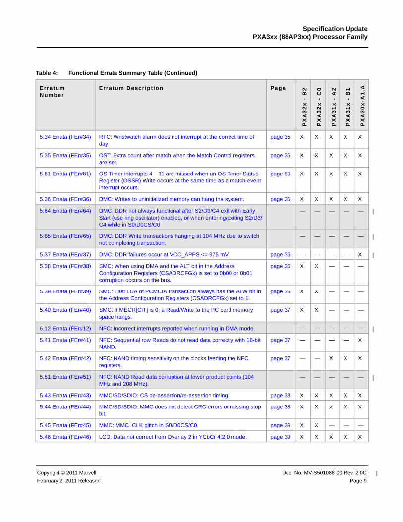
Table 4: Functional Errata Summary Table
Erratum Number
Erratum Descript ion PageP
XA
32
x -
B2
PX
A3
2x
- C
0
PX
A3
1x
- A
2
PX
A3
1x
- B
1
PX
A3
0x
-A1
.A
5.1 Errata (FEr#1) ROM: Boot ROM reconfigures pads on S2/D3/C4 exit. page 13 NB NB — — —
5.2 Errata (FEr#2) ROM: Unable to exit S2/D3/C4 to DDR when fused for NAND boot.
page 14 NB NB — — —
5.3 Errata (FEr#3) ROM: First 32 KB of SRAM is locked when the processor exits Low power modes and resets.
page 14 X — — — —
5.4 Errata (FEr#4) ROM: The ICCR[DIM] register gets set when coming out of all resets.
page 15 X — — — —
5.5 Errata (FEr#5) ROM: First 1 KB of SRAM is locked when the processor exits Low power mode and resets.
page 15 X X X X X
5.6 Errata (FEr#6) ROM: The Boot ROM issues a reset after power on reset that can cause boot failures.
— — — — —

Copyright © 2011 Marvell Doc. No. MV-S501088-00 Rev. 2.0C
February 2, 2011 Released Page 7
Specification UpdatePXA3xx (88AP3xx) Processor Family
5.80 Errata (FEr#80) ROM: Boot ROM clears the OS Timer Count Register 0 (OSCR0) register while handling resets.
page 50 — — X X X
5.6 Errata (FEr#6) CORE: L1 cache maintenance operations close to mem ops can overlock the L1 D-cache.
page 15 X X X X X
5.7 Errata (FEr#7) CORE: Locking all eight ways in L2 causes the core to hang. page 16 X X — — —
5.8 Errata (FEr#8) CORE: Debug - hold reset cannot be set before reset is asserted. page 17 X X X X X
5.9 Errata (FEr#9) CORE: A rejected request is retried out of order at the core interface.
page 17 X X — — —
5.10 Errata (FEr#10) CORE: dbg txrxctl rr bit gets set when it should not. page 18 X X X X X
5.11 Errata (FEr#11) CORE: Aborted PLD sets lock bit. page 18 X X X X X
5.12 Errata (FEr#12) CORE: In Special Debug State, data can return twice to a register for an aborting load.
page 21 X X X X X
5.18 Errata (FEr#18) CORE: Possible instruction corruption during page table Read. — — — — —
5.19 Errata (FEr#19) CORE: Possible Page table corruption during Read. — — — — —
5.13 Errata (FEr#13) Core: Data Cache Unit (DCU1) hangs in an infinite recirculate loop which results in data not being returned to the register file.
page 22 X X — — X
5.14 Errata (FEr#14) Core: Data Cache Unit (DCU2) Hang with Strongly Ordered Memory
page 23 X X — — —
5.15 Errata (FEr#15) Core: System hangs occur while changing operating points when two back to back reads from internal SRAM, the Static Memory Controller, the Dynamic Memory Controller, System Bus 1/System Bus 2 or between the system buses occur.
page 24 X — X — X
5.76 Errata (FEr#76) CORE: Random system hangs may occur when exiting S0/D0CS/C1
page 48 X — X — X
5.16 Errata (FEr#16) PIN CONTROL: Glitches can occur when entering low power mode (S0/D1/C2, S0/D2/C2 and S2/D3/C4)
page 24 X X — — X
5.17 Errata (FEr#17) PIN CONTROL: Signals can glitch while entering a hardware or GPIO reset
page 25 X X — — —
5.18 Errata (FEr#18) PIN CONTROL: Signals can glitch when a BATT_FAULT occurs. page 25 X X X X X
5.19 Errata (FEr#19) CLK: Ring oscillator frequency may go out of spec leading to UART failures.
page 25 X X — — X
5.20 Errata (FEr#20) PMU: When leaving S3/D4/C4, command to reset the voltages not sent to PMIC.
page 25 X X X X X
Table 4: Functional Errata Summary Table (Continued)
Erratum Number
Erratum Description Page
PX
A3
2x
- B
2
PX
A3
2x
- C
0
PX
A3
1x
- A
2
PX
A3
1x
- B
1
PX
A3
0x
-A1
.A

Doc. No. MV-S501088-00 Rev. 2.0C Copyright © 2011 Marvell
Page 8 February 2, 2011 Released
Specification Update PXA3xx (88AP3xx) Processor Family
5.21 Errata (FEr#21) PMU: When ACCR[PCCE] = 1 the AGENP[RO_ST] (MP-6377) may not reflect the correct status of the 120 MHz right oscillator.
page 26 X X X X X
5.22 Errata (FEr#22) APMU: System hangs may occur when three separate operations execute between the Application Subsystem Power Management Unit (APMU), Application Subsystem Clock Control Unit (ACCU) OS Timers (OST), and Intel XScale® core.
page 26 X X X X X
5.23 Errata (FEr#23) APMU: Any Writes to the Application Subsystem Interrupt Control/Status Register (AICSR) register clear the interrupt status bits.
page 30 X X X X X
5.24 Errata (FEr#24) SERVICES: GPIO reset wakes up the processor from S3/D4/C4. page 30 X X X X X
5.25 Errata (FEr#25) SERVICES: Unexpected PWR_I2C commands sent on ACCR write.
page 30 X X X X X
5.26 Errata (FEr#26) SERVICES: Two sets of PWR I2C sent on S2 exit. page 30 X X X X X
5.49 Errata (FEr#49) SERVICES: 13 MHz stability counter too small (similar to start-of-day problem).
— — — — —
5.27 Errata (FEr#27) SERVICES: nRESET_IN ignored during start-of-day when VCC_BBATT is less than 2.4V.
page 31 X X X X X
5.52 Errata (FEr#52) SERVICES: BATT_FAULT status bit not set between SYS_EN and PWR_EN on a hardware reset.
— — — — —
5.28 Errata (FEr#28) SERVICES: SRAM is not retained during a GPIO RESET, and the Boot ROM resumes to SRAM in Non-debug mode.
page 31 X X — — —
5.29 Errata (FEr#29) SERVICES: Lockup occurs if nBATT_FAULT asserted after sys_Del count is done and the battery does not have enough energy to complete Start-of-Day sequence.
page 31 X X — — —
5.30 Errata (FEr#30) SERVICES: System hangs may occur when increasing operating points from 208 MHz or 416 MHz, or when using 806 MHz or 416 MHz Idle modes.
page 32 X — X — X
5.82 Errata (FEr#82) SERVICES: EXT_WAKEUP<1:0> wakes up on both rising and falling edges regardless of PWER[WEx[1:0]] settings.
page 51 X X X X X
5.31 Errata (FEr#31) 1-WIRE: Reads bad data when Receive-Buffer-Full status bit is set.
page 33 X X X X X
5.32 Errata (FEr#32) 1-WIRE: PD flag not cleared when read (when interrupts are disabled).
page 34 X X X X X
5.33 Errata (FEr#33) INTERRUPT CONTROLLER: Unexpected exception vector when ICCR[DIM]=0 and ICMR=0.
page 34 X X X X X
Table 4: Functional Errata Summary Table (Continued)
Erratum Number
Erratum Descript ion Page
PX
A3
2x
- B
2
PX
A3
2x
- C
0
PX
A3
1x
- A
2
PX
A3
1x
- B
1
PX
A3
0x
-A1
.A
Copyright © 2011 Marvell Doc. No. MV-S501088-00 Rev. 2.0C
February 2, 2011 Released Page 9
Specification UpdatePXA3xx (88AP3xx) Processor Family
5.34 Errata (FEr#34) RTC: Wristwatch alarm does not interrupt at the correct time of day
page 35 X X X X X
5.35 Errata (FEr#35) OST: Extra count after match when the Match Control registers are set.
page 35 X X X X X
5.81 Errata (FEr#81) OS Timer interrupts 4 – 11 are missed when an OS Timer Status Register (OSSR) Write occurs at the same time as a match-event interrupt occurs.
page 50 X X X X X
5.36 Errata (FEr#36) DMC: Writes to uninitialized memory can hang the system. page 35 X X X X X
5.64 Errata (FEr#64) DMC: DDR not always functional after S2/D3/C4 exit with Early Start (use ring oscillator) enabled, or when entering/exiting S2/D3/C4 while in S0/D0CS/C0
— — — — —
5.65 Errata (FEr#65) DMC: DDR Write transactions hanging at 104 MHz due to switch not completing transaction.
— — — — —
5.37 Errata (FEr#37) DMC: DDR failures occur at VCC_APPS <= 975 mV. page 36 — — — — X
5.38 Errata (FEr#38) SMC: When using DMA and the ALT bit in the Address Configuration Registers (CSADRCFGx) is set to 0b00 or 0b01 corruption occurs on the bus.
page 36 X X — — —
5.39 Errata (FEr#39) SMC: Last LUA of PCMCIA transaction always has the ALW bit in the Address Configuration Registers (CSADRCFGx) set to 1.
page 36 X X — — —
5.40 Errata (FEr#40) SMC: If MECR[CIT] is 0, a Read/Write to the PC card memory space hangs.
page 37 X X — — —
6.12 Errata (FEr#12) NFC: Incorrect interrupts reported when running in DMA mode. — — — — —
5.41 Errata (FEr#41) NFC: Sequential row Reads do not read data correctly with 16-bit NAND.
page 37 — — — — X
5.42 Errata (FEr#42) NFC: NAND timing sensitivity on the clocks feeding the NFC registers.
page 37 — — X X X
5.51 Errata (FEr#51) NFC: NAND Read data corruption at lower product points (104 MHz and 208 MHz).
— — — — —
5.43 Errata (FEr#43) MMC/SD/SDIO: CS de-assertion/re-assertion timing. page 38 X X X X X
5.44 Errata (FEr#44) MMC/SD/SDIO: MMC does not detect CRC errors or missing stop bit.
page 38 X X X X X
5.45 Errata (FEr#45) MMC: MMC_CLK glitch in S0/D0CS/C0. page 39 X X — — —
5.46 Errata (FEr#46) LCD: Data not correct from Overlay 2 in YCbCr 4:2:0 mode. page 39 X X X X X
Table 4: Functional Errata Summary Table (Continued)
Erratum Number
Erratum Description Page
PX
A3
2x
- B
2
PX
A3
2x
- C
0
PX
A3
1x
- A
2
PX
A3
1x
- B
1
PX
A3
0x
-A1
.A

Doc. No. MV-S501088-00 Rev. 2.0C Copyright © 2011 Marvell
Page 10 February 2, 2011 Released
Specification Update PXA3xx (88AP3xx) Processor Family
5.47 Errata (FEr#47) LCD artifacts occur when exiting S0/D1/C2. page 39 — — X X X
5.48 Errata (FEr#48) LCD: VGA screens not supported when using S0/D1/C2 mode. page 40 — — X X X
5.49 Errata (FEr#49) LCD: Insufficient bandwidth to support 640x480 screens when using DDR for the Frame buffer in S0/D0CS/C0 mode.
page 40 X — — — X
5.50 Errata (FEr#50) LCD: The MSB acts as both the T-bit and red color when using RGB565 with Chroma Keying enabled on Overlay 1 and Overlay 2.
page 40 — — X X —
5.77 Errata (FEr#77) LCD: VGA Input and Output FIFO under-runs can occur while running in S0/D0CS/C0.
page 49 — — X X —
5.51 Errata (FEr#51) CI: CGC LUT load gets corrupted due to READ/WRITE pointer collision.
page 40 X X X X X
5.52 Errata (FEr#52) CI: Camera FIFO overflow when slow memory accesses occur. page 41 X X X X X
5.53 Errata (FEr#53) CI: Scaling unit computes bad values for Y value of YCrCb scaling.
page 41 X X — — —
5.78 Errata (FEr#78) CI: QCI will capture one line of invalid data page 49 X X X X X
5.54 Errata (FEr#54) GCU: STR_BLT instruction hangs when Source and Destination buffers are in external SRAM, does not return correct data occasionally when buffers are in DDR.
page 41 X X — — X
5.55 Errata (FEr#55) GCU: Pattern copy fails for random test cases with data mismatch. page 42 X X X X X
5.56 Errata (FEr#56) KEYPAD: Wrong clock divider in S0/D0CS/C0 mode is causing keypress detection problems.
page 42 X X — — —
5.57 Errata (FEr#57) TSI: TSI controller takes almost 2 ms to start up after exiting Low-power mode.
page 42 X X — — —
5.58 Errata (FEr#58) TSI: Discontinuity in A/D conversions near 64-count boundaries in 12- bit mode.
page 42 X X — — —
5.59 Errata (FEr#59) TSI exhibits differing conversion times. page 43 X X — — —
5.60 Errata (FEr#60) TSI: Steady state conversion variability > 4 counts. page 43 X X — — —
5.61 Errata (FEr#61) TSI: ADCS[RUN] not cleared by TSI state machine page 43 X X — — —
5.62 Errata (FEr#62) TSI: Stylus-up interrupt not reliably generated when XY=1, CC=0, also generating extra Stylus down/up interrupts in continuous conversion (XY=1, CC=1).
page 43 X X — — —
5.63 Errata (FEr#63) UDC: FIFO content of an IN endpoint not flushed by FEF when double-buffered
page 45 X X — — X
Table 4: Functional Errata Summary Table (Continued)
Erratum Number
Erratum Descript ion Page
PX
A3
2x
- B
2
PX
A3
2x
- C
0
PX
A3
1x
- A
2
PX
A3
1x
- B
1
PX
A3
0x
-A1
.A

Copyright © 2011 Marvell Doc. No. MV-S501088-00 Rev. 2.0C
February 2, 2011 Released Page 11
Specification UpdatePXA3xx (88AP3xx) Processor Family
5.64 Errata (FEr#64) U2DC: Corrupted EOP in Full-speed mode causes the U2D to hang.
page 45 X X — — X
5.65 Errata (FEr#65) U2DC: DMA Control/Status register reports “end of Receive” interrupt on “IN” endpoints
page 45 X X — — X
6.47 Errata (FEr#47) U2DC: DMA not writing data correctly to FIFO when source address is not 8-byte aligned.
— — — — —
6.48 Errata (FEr#48) U2DC: Stopping DMA when SP interrupt occurs causes DMA status error.
— — — — —
5.66 Errata (FEr#66) U2DC: Internal USB host/client resistors may be out of spec above 40 degrees C.
page 45 X X — — —
6.50 Errata (FEr#50) U2DC: IN endpoint sends incorrect data and causes a NAK on OUT transfers, if the DMA is started for the next transfer before the FIFO is empty.
— — — — —
6.51 Errata (FEr#51) U2DC: Endpoints with default alternate setting in non-zero interface send STALL after SET CONFIGURATION.
— — — — —
6.52 Errata (FEr#52) U2DC: Signals between U2D and the system bus can be missed at a bus clock frequency of 104 MHz.
— — — — —
6.53 Errata (FEr#53) U2DC: Stall on PING token packets (bulk out or EP0 out) may have incorrect response.
— — — — —
6.54 Errata (FEr#54) U2DC: Setting FST does not STALL an endpoint not affected by an active SET_INTERFACE
— — — — —
6.55 Errata (FEr#55) U2DC: STALL response when an incoming host request collides with an Endpoint FIFO flush.
— — — — —
5.69 Errata (FEr#69) ULPI_STP asserts upon exiting S0/D1/C2 and S0/D2/C2 modes. — — — — —
5.67 Errata (FEr#67) USBH: USB host Port 3 in Transceiverless mode may not work correctly with an external device.
page 46 X X — — X
5.68 Errata (FEr#68) USBH: USB host fails with system bus = 104 MHz or 208 MHz. page 46 — — — — X
5.69 Errata (FEr#69) SSP: EOR is not set when FIFO Packed mode is used. page 46 X X X X X
5.70 Errata (FEr#70) SSP: SSP not functional when entering and exiting S0/D0CS/C0 prior to enabling SSP.
page 47 X X — — —
5.71 Errata (FEr#71) UART: When DLL and DLH are programmed at the same time, UART takes in only the first one.
page 47 X X X X X
5.72 Errata (FEr#72) UART: TX interrupt can be missed when running full duplex page 47 X X — — X
Table 4: Functional Errata Summary Table (Continued)
Erratum Number
Erratum Description Page
PX
A3
2x
- B
2
PX
A3
2x
- C
0
PX
A3
1x
- A
2
PX
A3
1x
- B
1
PX
A3
0x
-A1
.A

Doc. No. MV-S501088-00 Rev. 2.0C Copyright © 2011 Marvell
Page 12 February 2, 2011 Released
Specification Update PXA3xx (88AP3xx) Processor Family
5.73 Errata (FEr#73) CIR: Wrong symbols sent on second transmission after boot. page 48 X X X X X
5.74 Errata (FEr#74) I2C: Bus Busy bit only changes on state transitions. page 48 X X X X X
5.75 Errata (FEr#75) I2C: Enabling I2C unit drives SCL low. page 48 X X — — —
5.79 Errata (FEr#79) The I2C Unit Not Busy bit (ISR[UB]) remains set after Master Abort
page 50 X X X X X
Table 4: Functional Errata Summary Table (Continued)
Erratum Number
Erratum Descript ion Page
PX
A3
2x
- B
2
PX
A3
2x
- C
0
PX
A3
1x
- A
2
PX
A3
1x
- B
1
PX
A3
0x
-A1
.A

Copyright © 2011 Marvell Doc. No. MV-S501088-00 Rev. 2.0C
February 2, 2011 Released Page 13
Specification UpdatePXA3xx (88AP3xx) Processor Family
5. Detailed Descriptions for Functional ErrataRefer to Section Table 4: "Functional Errata Summary Table" on page 6 to determine which errata are new to this report.
5.1 Errata (FEr#1)Type: Functional ErrataRelevant for: PXA32x - AllFixed in: No BugErrata BTS#: MP-5737Description: ROM: Boot ROM reconfigures pads on S2/D3/C4 exit.Problem: The Boot ROM reconfigures MFPRs on S2/D3/C4 exit. These registers should not be modified by the
Boot ROM.Implication: For a Resume on a non-trusted NAND platform, the Resume address is taken from the PSPR register
and Resume transfers to ISRAM and no MFPR pads are set. Refer to Table 5 for Multi-Function PinRegister (MFPR) Boot ROM configurations. Procedures required for exiting S2/D3/C4 are documentedin the PXA3xx Processors Boot ROM Reference Manual.
Table 5: Multi-Function Register Pin (MFPR) Settings
Ball Name Address Value
GPIO2 0x40E1_012C 0x0000_0001
GPIO3 0x40E1_0134 0x0000_0001
GPIO4 0x40E1_0134 0x0000_0001
nXCVREN 0x40E1_0138 0x0000_1900
nBE0 0x40E1_0214 0x0000_1800
nBE1 0x40E1_0218 0x0000_1800
nLUA 0x40E1_0234 0x0000_1900
nLLA 0x40E1_0238 0x0000_1900
DF_ADDR0 0x40E1_023C 0x0000_1800
DF_ADDR1 0x40E1_0240 0x0000_1800
DF_ADDR2 0x40E1_0244 0x0000_1800
DF_ADDR3 0x40E1_0248 0x0000_1800
DF_CLE 0x40E1_0204 0x0000_1800
DF_ALE_NWE1 0x40E1_0208 0x0000_1801
DF_IO0 0x40E1_024C 0x0000_1401
DF_IO1 0x40E1_0254 0x0000_1401
DF_IO2 0x40E1_025C 0x0000_1401
DF_IO3 0x40E1_0264 0x0000_1401
DF_IO4 0x40E1_026C 0x0000_1401
DF_IO5 0x40E1_0274 0x0000_1401

Doc. No. MV-S501088-00 Rev. 2.0C Copyright © 2011 Marvell
Page 14 February 2, 2011 Released
Specification Update PXA3xx (88AP3xx) Processor Family
Workaround: The MFPRs must be reconfigured by software after S2/D3/C4 exit.
5.2 Errata (FEr#2)Type: Functional ErrataRelevant for: PXA32x - AllFixed in: No BugErrata BTS#: MP-5942Description: ROM: Unable to exit S2/D3/C4 to DDR when fused for NAND boot.Problem: When fused for NAND boot, it is not possible to exit S2/D3/C4 and boot to DDR.Implication: Cannot directly go from S2/D3/C4 to DDR execution.Workaround: The Boot ROM does not currently support direct exit from S2/D3/C4 to DDR. The first bank of SRAM
must be kept on while in S2/D3/C4. The procedures for exiting S2/D3/C4 are documented in the PXA3xxProcessors Boot ROM Reference Manual and do not include resuming from DDR.
5.3 Errata (FEr#3)Type: Functional ErrataRelevant for: PXA32x - B2Fixed in: PXA32x - C0Errata BTS#: ML-989Description: ROM: First 32 KB of SRAM is locked when the processor exits Low power modes and resets.Problem: In non-trusted boot, the Wireless Trusted Module (WTM) locks the first 32 KB of internal SRAM.Implication: Software requiring access to this 32 KB of SRAM is unable to do so.Workaround:
Software Workaround
Coming out of hardware/GPIO/watchdog reset or S3/D4/C4 mode:
1. Set the CTMCR[0] (0x4300_0010) bit after BOOTROM hands control to OBM. 2. Disable the WTM clock by clearing D0CKEN_A[CKEN[19]] register.
DF_IO6 0x40E1_027C 0x0000_1401
DF_IO7 0x40E1_0284 0x0000_1401
DF_IO8 0x40E1_0250 0x0000_1401
DF_IO9 0x40E1_0258 0x0000_1401
DF_IO10 0x40E1_0260 0x0000_1401
DF_IO11 0x40E1_0268 0x0000_1401
DF_IO12 0x40E1_0270 0x0000_1401
DF_IO13 0x40E1_0278 0x0000_1401
DF_IO14 0x40E1_0280 0x0000_1401
DF_IO15 0x40E1_0288 0x0000_1401
Table 5: Multi-Function Register Pin (MFPR) Settings (Continued)
Ball Name Address Value

Copyright © 2011 Marvell Doc. No. MV-S501088-00 Rev. 2.0C
February 2, 2011 Released Page 15
Specification UpdatePXA3xx (88AP3xx) Processor Family
Going into S2/D3/C4:
1. Enable WTM clock by setting the D0CKEN_A[CKEN[19]] register. 2. Enable Mini-LCD clocks by setting DOCKEN_B[CKEN[17]] register if it is not enabled.
Coming out of S2/D3/C4:
1. D0CKEN_A[CKEN[19]] and D0CKEN_B[CKEN[17]] can be disabled to save power.
5.4 Errata (FEr#4)Type: Functional ErrataRelevant for: PXA32x - B2 Fixed in: PXA32x - C0Errata BTS#: MLV-1762Description: ROM: The ICCR[DIM] register gets set when coming out of all resets.Problem: Coming out of all resets, the Boot ROM sets the ICCR[DIM] register.Implication: By setting the ICCR[DIM] register only active, unmasked interrupts as defined in the ICMR register bring
the processor out of S0/D0/C1 modes. This bit is ignored in the S0/D0/C0 run mode.Workaround: Software must clear this register after a reset to detect wakeups from the sources defined in the ICPR
registers when running in S0/D0/C1 mode.
5.5 Errata (FEr#5)Type: Functional ErrataRelevant for: PXA30x-All, PXA31x-All, PXA320-AllFixed in: No FixErrata BTS#: ML-989Description: ROM: First 1 KB of SRAM is locked when the processor exits Low power mode and resets.Problem: In Non-Trusted boot, the Wireless Trusted Module (WTM) locks the first 1 KB of internal SRAM.Implication: Software requiring access to this 1 KB of SRAM is unable to access it.Workaround:
Software Workaround
Coming out of hardware/GPIO/watchdog reset or S3/D4/C4 mode:
1. Set the CTMCR[0] (0x4300_0010) bit after BOOTROM hands control to OBM. 2. Disable the WTM clock by clearing D0CKEN_A[CKEN[19]] register.
Going into S2/D3/C4:
1. Enable WTM clock by setting the D0CKEN_A[CKEN[19]] register. 2. Enable Mini-LCD clocks by setting DOCKEN_B[CKEN[17]] register if it is not enabled.
Coming out of S2/D3/C4:
1. D0CKEN_A[CKEN[19]] and D0CKEN_B[CKEN[17]] can be disabled to save power.
5.6 Errata (FEr#6)Type: Functional ErrataRelevant for: PXA32x - All, PXA30x - All, PXA31x-AllFixed in: No FixErrata BTS#: Core ARS 3584Description: CORE: L1 cache maintenance operations close to mem ops can overlock the L1 D-cache.Problem: Results in locations being locked into the L1 data cache incorrectly.

Doc. No. MV-S501088-00 Rev. 2.0C Copyright © 2011 Marvell
Page 16 February 2, 2011 Released
Specification Update PXA3xx (88AP3xx) Processor Family
Memory operations when the L1 data cache is set up for locking (Bit 0 of the L1 Data Cache Lock registeris set) can set the lock bit for a different line as well as the preferred line, within the same set. This occurswhen the memory operation stalls in the data-cache pipeline due to a L1 cache maintenance instructionpreceding the memory operation.
This bug is similar to errata #3544. This affects locking into the L1 data cache only. Locking the L1 in-struction cache or the L2 cache are not affected. This bug can occur only during the process of lockingdata into the L1 data cache. Once the data cache has been locked down, the bug has no impact.
Steps that expose the bug:
1. Enable DCU locking2. Perform an L1 cache maintenance operation (defined in subsequent paragraphs)3. Perform a memory operation followed immediately by a cache-maintenance operation. This
sequence is stalled in the third data-cache stage of the pipe by the cache-maintenance operation.
A full list of affected L1 cache maintenance commands follows:
mcr p15, 0, Rd, c7, c6, 1 - Invalidate L1 D-cache by MVAmcr p15, 0, Rd, c7, c10, 1 - Clean L1 D-cache by MVAmcr p15, 0, Rd, c7, c10, 2 - Clean L1 D-cache by set/waymcr p15, 0, Rd, c7, c14, 1 - Clean and invalidate L1 D-cache by MVAmcr p15, 0, Rd, c7, c14, 2 - Clean and invalidate L1 D-cache by set/way
Implication: A location in the same set of the L1 data cache as the stalled memory operation in Step 3 above maybe locked and not available for allocation. Data is not modified or corrupted.
Workaround: Two workarounds exist:
Workaround #1: Do not perform L1 cache-control commands while in DCU locking mode.Workaround #2: Possible: Separate L1 cache-control commands by at least a single non-memory op-eration instruction while in DCU locking mode to avoid the stall condition.
5.7 Errata (FEr#7)Type: Functional ErrataRelevant for: PXA32x - AllFixed in: No FixErrata BTS#: Core ARS 3251Description: CORE: Locking all eight ways in L2 causes the core to hang.Problem: The replacement behavior on a miss in the L2 cache on a line where all eight ways have been locked is
defined as “architecturally unpredictable.” However, the implementation treats “all ways locked” as “noways locked”, and as such, normal replacement schemes (excluding lock behavior) dictate which linegets replaced.
A corner case is associated with this condition. Normally, when all ways are locked in the L2, the lockbits would be ignored and find the first way that is “not used and not pend” for selecting a replacement.However, in certain situations, there is no way left that is “not used and not pend”. The result is that the

Copyright © 2011 Marvell Doc. No. MV-S501088-00 Rev. 2.0C
February 2, 2011 Released Page 17
Specification UpdatePXA3xx (88AP3xx) Processor Family
default replacement is used, and a way that is marked PEND is replaced erroneously.Implication: Locking all eight ways in L2 causes the core to hang.Workaround: Do not lock all eight ways.
5.8 Errata (FEr#8)Type: Functional ErrataRelevant for: PXA32x - All, PXA30x - All, PXA31x - AllFixed in: No FixErrata BTS#: Core ARS 3401Description: CORE: Debug - hold reset cannot be set before reset is asserted.Problem: The hold_reset bit (accessed through JTAG in DCSR data reg) is what the debugger uses to hold the
core in reset while the debugger downloads the debug handler into the SRAM. Typically, a user wouldset this bit during reset assertion to the chip (and core). Prior to the PXA3xx (88AP3xx) Processor Familycore, the debugger could also set this bit even when the core was not in reset, but it would not have anyeffect until the next core reset. The core would stay in reset until the debugger cleared the keep_resetbit.
On the PXA3xx (88AP3xx) Processor Family core, setting this bit prior to reset results in unpredictablebehavior when the core comes out of reset. The problem is that while this bit is set, some internal corestates are not reset. So, setting this bit during reset (specifically, after the core enters reset) works be-cause there is a point when the core is in reset, but keep_reset has yet to be set by the debugger. Settingthis bit prior to reset means when the reset occurs, there is no time at which reset is asserted withoutkeep_reset also being asserted. So this latter case results in some core states not being reset. After re-set, this process results in unpredictable operation of the core.
This feature is not commonly used, and with the addition of hot-debug hardware to the core, the newhot-debug capabilities provide an alternative solution. Also, since vendors will be using the new hot-de-bug features (regardless of this keep_reset issue), there is no significant impact on the tools.
Implication: PXA3xx (88AP3xx) Processor Family core debug features are not compatible with the PXA27x core.Workaround: The debugger must set the keep_reset bit only after the core has already entered reset. Setting this bit
while the core is not already in reset results in unpredictable core behavior.
5.9 Errata (FEr#9)Type: Functional ErrataRelevant for: PXA32x - AllFixed in: No FixErrata BTS#: Core ARS 3501Description: CORE: A rejected request is retried out of order at the core interface.Problem: If all the conditions below occur, the L1 data cache clean command may proceed when there are no
available buffers. Whether it hits or misses, it corrupts a buffer, which can lead to unpredictable behavior.
Steps that expose the bug:1.The following code sequence (back to back, with no intervening instructions):
a) Any memory operation (Load, Store, Cache Management operation, etc.)b) L2 cache control command (Clean, Invalidate, etc.)c) L1 data cache clean command (by MVA or by set/way)
2.The Memory buffers are full (heavy recent load/store traffic).3.Two memory transactions complete within 1-2 cycles freeing up their buffers.

Doc. No. MV-S501088-00 Rev. 2.0C Copyright © 2011 Marvell
Page 18 February 2, 2011 Released
Specification Update PXA3xx (88AP3xx) Processor Family
This situation can occur even if all pages are marked as writethrough. The Clean command does not have to hit the cache or hit dirty data for the bug to occur.
Implication: Possible symptoms:• Dropped memory transaction (load or store)
• Part hangs• Incorrect data stored out• Incorrect data returned to a register
Workaround: Separate L1 and L2 cache control commands by at least a single non-cache control instruction.
5.10 Errata (FEr#10)Type: Functional ErrataRelevant for: PXA32x - All, PXA30x - All, PXA31x - AllFixed in: No FixErrata BTS#: Core ARS 3551Description: CORE: dbg txrxctl rr bit gets set when it should not.Problem: This bug occurs when the RX register has a new valid value loaded into it and the rx_valid bit is then
polled by the external debugger to determine if the core has read the value. There is a window (approx-imately six TCK cycles) between the update-DR in the JTAG polling loop of the rx_valid bit and the read-ing of the RX register by the core software. The read of the RX register by the core clears theTXRXCTL[RR] flag but the polling of the rx_valid bit via JTAG in this window can set the TXRXCTL[RR]flag erroneously again.
Implication: When software running on the core communicates to an external debugger, the TXRXCTL[RR] flag canbe set erroneously even when there has not been a new DBGRX update sent in via JTAG. In otherwords, the core software can “think” it has received a new RX data value when, in fact, the debugger didnot send a new value.
Workaround: Two workarounds exist:
Workaround #1: Use the debug handler recommended by Marvell.Workaround #2: A software workaround for custom debug-handler software is as follows:
–Modify the core software so that after the core reads the RX register, it transmits an “acknowledgement” message containing some recognizable data value to the debugger via the DBGTX register signaling that it has read the RX register.
–The debugger should have a corresponding modification so that it does not poll the DBGRX register again (after sending a valid message) until it “sees” the core software acknowledgement message. Once it detects the acknowledgement message, it can either poll DBGRX or send another message.
5.11 Errata (FEr#11)Type: Functional ErrataRelevant for: PXA32x - All, PXA30x - All, LV-allFixed in: No FixErrata BTS#: Core ARS 3558Description: CORE: Aborted PLD sets lock bit.Problem: This issue results in locations being locked in the cache incorrectly. If a PLD instruction that does not
have permission to access a given memory region is used during data-cache locking, then the DCU mayincorrectly lock a “hole” into the data cache, effectively reducing the data cache size by one line.

Copyright © 2011 Marvell Doc. No. MV-S501088-00 Rev. 2.0C
February 2, 2011 Released Page 19
Specification UpdatePXA3xx (88AP3xx) Processor Family
PLD instructions are defined to NOT abort – that is, if they do not have permission to access a line frommemory; they are supposed to turn into a NOP: the data cache should not be updated. In this bug, thedata cache is updated with a locked invalid line.
Steps that expose the bug:1. Enable L1 data-cache locking.2. Perform a PLD instruction that does not have permission.
Implication: This process affects locking into the L1 data cache only. Locking the L1 instruction cache or the L2cache are not affected.
This bug can occur only during the process of locking data into the L1 data cache. Once the data cachehas been locked down, the bug has no impact.
Data aborts taken while the lock bit is set are dangerous because memory operations executed in theabort handler will be locked.
Workaround: Use the L1 locking routine specified below or in the PXA3xx (88AP3xx) Processor Family Software De-velopers Guide:
@ Restrictions:
@
@ Prefetch abort handler MUST turn off lock mode bit
@ as soon as possible.
@
@ Data abort handler MUST turn off lock mode bit as
@ soon as possible.
@
@ If there are any imprecise aborts during locking
@ the result of locking is unpredictable.
@
@ PSR bit defines
.setPSR_I, 0x80
.setPSR_F, 0x40
@ LockDCache flags
.setL_LEN, 0x01
.setL_INV, 0x02
@ Data Cache Lock Mode
.setM_LOCKED, 0x01
.setM_NOT_LOCKED, 0x00
@ Cache Line Size
.setLINE_SIZE, 0x20
@
@ _LockDCache(Start,End_or_Length,Flags)
@
@ Inputs
@ R0 Start Address
@ R1 End Address (inclusive) or Length

Doc. No. MV-S501088-00 Rev. 2.0C Copyright © 2011 Marvell
Page 20 February 2, 2011 Released
Specification Update PXA3xx (88AP3xx) Processor Family
@ R2 Flags
@
@ Outputs
@ R0 Success (1) / Failure (0)
@
@ Registers used
@ R1 - R3, IP
@
@ Usage:
@
@ If a region length is specified in R1 then the
@ L_LEN flag must be set. All data cache will be
@ unlocked and invalidated if the L_INV flag is set.
@ If several things are to be locked into the cache
@ the L_INV flag should be set for the first item
@ to be locked and clear for subsequent items.
@
.align 2
.global _LockDCache
.type _LockDCache,function
_LockDCache:
mrs ip, cpsr @ Save CPSR
orr r3, ip, #PSR_I | PSR_F
msr cpsr_c, r3 @ Disable Interrupts
mrc p15, 0, r3, 1, 0, 0
mcr p15, 0, r3, 1, 0, 0 @ Force a DCU drain
tst r2, #L_INV
mcrne p15, 0, r0, c9, c6, 1 @ Unlock D-Cache
mcrne p15, 0, r0, c7, c6, 0 @ Invalidate D-Cache
mov r3, #M_LOCKED
mcr p15, 0, r3, c9, c6, 0 @ Set Lock Mode
tst r2, #L_LEN
addne r1, r1, r0
cmpne r1, r0
subne r1, r1, #1
CacheFill:
@ Uncomment the DCU drain code for REV A0 silicon
ldr r2, [r0], #LINE_SIZE
@ mrc p15, 0, r3, 1, 0, 0
@ mcr p15, 0, r3, 1, 0, 0 @ Force a DCU drain
cmp r0, r1
ldrls r3, [r0], #LINE_SIZE
@ mrcls p15, 0, r3, 1, 0, 0
@ mcrls p15, 0, r3, 1, 0, 0 @ Force a DCU drain

Copyright © 2011 Marvell Doc. No. MV-S501088-00 Rev. 2.0C
February 2, 2011 Released Page 21
Specification UpdatePXA3xx (88AP3xx) Processor Family
cmpls r0, r1
bls CacheFill
orr r2, r2, r3 @ Create a dependency stall
mrc p15, 0, r0, c9, c6, 0 @ Read Lock Mode
mov r2, #M_NOT_LOCKED
mcr p15, 0, r2, c9, c6, 0 @ Clear Lock Mode
msr cpsr_f, ip @ Reset Interrupt flags
and r0, r0, #M_LOCKED @ Test lock flag
mov pc, lr
.Lfe1:
.size _LockDCache,.Lfe1-_LockDCache
5.12 Errata (FEr#12)Type: Functional ErrataRelevant for: PXA32x - All, PXA30x - All, PXA31x - AllFixed in: No FixErrata BTS#: Core ARS 3497Description: CORE: In Special Debug State, data can return twice to a register for an aborting load.Problem: This situation results in the DCU returning twice to a register for an aborting load in SDS (Special Debug
State).
In SDS, memory operations that would normally abort and cause an event flush do not. Instead, theyare supposed to cease operation; specifically, clear the scoreboard bit, and set the “sticky” abort bit inthe DCSR. For certain aborting loads, the DCU detects that the load is programmed to abort and clearthe scoreboard bit, but also sends out a memory request for the aborting load – additionally, the DCUthen returns the incorrect data to the register file.
Steps that expose the bug:1. An outstanding store in one of the DCU memory buffers has not been globally observed.2. A strongly ordered operation is executed (either a load or a store).3. Before the strongly ordered operation in (2) has been globally observed, a Load operation that
aborts is executed. Because of (1) and (2), the DCU incorrectly returns twice to the register file.
Implication: Special Debug State does not operate correctly.Workaround: A software workaround is appropriate since this bug occurs only during SDS.
Two workarounds exist:Workaround #1: Before executing any load that “could” data abort, perform a DCUDRAIN_WRITEBUFFER (dwb) command (defined below).
Workaround #2: Because any load in SDS may abort and return incorrect data to a register, check the“sticky” abort bit in the DCSR before using the data from the load in question. This bug does not occurif a DCU_DRAIN (defined below) command is executed before any of the data from the loads is used.Additionally, performing a DCU_DRAIN command before reading the “sticky” abort bit in the DCSR hasthe added benefit that any imprecise data aborts on the loads have set the abort bit before the data isused.1. Perform any number of Loads/Stores.2. Perform the following before the data from the Loads is used:
a) DCU_DRAIN

Doc. No. MV-S501088-00 Rev. 2.0C Copyright © 2011 Marvell
Page 22 February 2, 2011 Released
Specification Update PXA3xx (88AP3xx) Processor Family
b) Read the “sticky” abort bit and verify that no aborts have occurredc) Use the data from the Loads
DCU_DRAIN is defined as:
mrc p15, 0, r3, c1, c0, 0 @# read CP15 Control register
mcr p15, 0, r3, c1, c0, 0 @# write CP15 Control register
[the mcr stalls until the L1 D cache buffers have completely drained]
DCU_DRAIN_WRITEBUFFER is defined as:
mcr p15, 0, r0, c7, c10, 4 @# drain write buffer (dwb)
5.13 Errata (FEr#13)Type: Functional ErrataRelevant for: PXA32x - All, PXA30x - AllFixed in: No FixErrata BTS#: MP-6244, ML-981, MLV-1723Description: Core: Data Cache Unit (DCU1) hangs in an infinite recirculate loop which results in data not being re-
turned to the register file.Problem: With the L1 Data Cache cacheable -or- L1 Data Cache uncacheable and the L2 Cache cacheable, a
specific sequence of loads and stores to the Data Cache Unit and a specific sequence of data beingreturned within an extremely narrow timing window can cause the Data Cache Unit to hang in an infiniteloop.
Required conditions for replicating the issue with and without evictions (All Loads/Stores are to L1cacheable memory -or- L1 uncacheable and L2 cacheable memory):
1. A Load misses the L1 data cache and must cause an eviction of a clean cacheline in the same set. However, this first load is not necessary (which means the L1D eviction is not a necessary condition).
2. A store is being retried by the Data Cache Unit due to a backed up Bus Interface Unit.3. Four loads to the same cacheline that miss the data cache.4. The following timing conditions must then happen:
– Must have some other unrelated instructions with no register dependencies occurring between #3 and #5.
5. A load, which is to the same cacheline as the store in #2, misses the data cache.–The first Load in #3 gets its data back into the Data Cache Unit exactly one cycle after this load
gets executed.
– The Store in #2 still retries from the Data Cache Unit and one of the attempts happens exactly one cycle after this load gets executed.
– No dependencies on previous loads.
6. A Load, which is to the same cacheline as the four loads in #3, misses the data cache.– No dependencies on previous loads.
– Must be back-to-back with #5.
7. A Load operation to any address.– Must be back-to-back with #6.
Implication: If the Data Cache Unit encounters this condition, it enters an infinite loop, resulting in no data being re-turned and thereby, hanging the processor core.

Copyright © 2011 Marvell Doc. No. MV-S501088-00 Rev. 2.0C
February 2, 2011 Released Page 23
Specification UpdatePXA3xx (88AP3xx) Processor Family
Notes:– This issue has been observed only on an SOC not related to the PXA3xx processors while running
hand-tuned focus tests written to specifically reproduce this issue.
–The only way to exit this condition is to reset the XScale® core.
–Independent of L1 data cache operating in Writethrough or Writeback mode.
–Independent of whether L2 cache is present.
–Independent of Bus timings/ratios.
Workaround: No workaround. However, there is a recovery mechanism in the unlikely event that is does occur. If alockup does occur, the only way to exit this condition is to reset the processor core. Examining the tracebuffer after a reset provides information on the code sequencing (within 16 clock cycles) leading to thelockup. Once identified, code corrections can be made to eliminate the condition as listed in the "Re-quired Conditions" section above that created the lockup.
5.14 Errata (FEr#14)Type: Functional ErrataRelevant for: PXA32x - AllFixed in: No FixErrata BTS#: MP-6251, ML-983, MLV-1726Description: Core: Data Cache Unit (DCU2) Hang with Strongly Ordered MemoryProblem: With the L1 Data Cache cacheable -or- L1 Data Cache uncacheable and the L2 Cache cacheable, a
specific sequence of loads and stores to the Data Cache Unit with a strongly ordered load and a specificsequence of data being returned within an extremely narrow timing window can cause the Data CacheUnit to hang, thereby hanging the processor core.
Required Conditions (All Loads/Stores are to L1 cacheable memory -or- L1 uncacheable and L2 cache-able memory):
1.A load misses the data cache and must cause an eviction of a dirty cacheline.–This eviction has to land between #2 and #3.
2.Four loads to the same cacheline that miss the data cache. No dependencies on previous loads.3.A memory access that is Strongly Ordered within a few instruction cycles of #2. No dependencies on
loads in #2.
Implication: If the Data Cache Unit encounters this condition, the load to strongly ordered memory is dropped, neverreturning the data and thereby, hanging the processor core.
Notes:•"This issue has only been observed on the 8134x when running hand-tuned focus tests written to
specifically reproduce this issue.•"The only way to exit this condition is to reset the processor core.•"Independent of L1 data cache operating in write through or write back mode.
•"Independent of L2 cache being present or not.•"Independent of Bus timings/ratios.
Workaround: Two workarounds exist for this issue.
1.Convert all "Strongly Ordered Memory" operations into "Device Memory" operations inside the Kernel. Where memory is configured as Strongly Ordered (in the page table, the following bits are set TEX=000b and CB=00b) the memory should be changed to be configured as Device Memory (in the page table, the following bits are set (TEX=010b and CB=00b for non-shared device memory) -or-

Doc. No. MV-S501088-00 Rev. 2.0C Copyright © 2011 Marvell
Page 24 February 2, 2011 Released
Specification Update PXA3xx (88AP3xx) Processor Family
(TEX=001b and CB=01 for shared device memory).
Small Page Descriptors cannot specify the TEX attribute. In this case, the TEX attribute will default to 0. If CB=00b is used with Small Page Descriptors, a Strongly Ordered Memory region is created. Therefore, do not use Small Page Descriptors; use Extended Small Page Descriptors instead.
2.This is more of a recovery mechanism (not a workaround) in the unlikely event that does occur. If a lockup does occur, the only way to exit this condition is to reset the processor core. Examining the trace buffer after a reset would give information on the code sequencing (within 16 clock cycles) leading to the lockup. Once identified, code corrections can be made to eliminate the condition as listed in the "Required Conditions" section above that created the lockup.
5.15 Errata (FEr#15 )Type: Functional ErratumRelevant for: PXA32x - B2, PXA31x - A2, PXA30x - AllFixed in: PXA32x - C0, PXA31x - B1, PXA30x - No FixErrata BTS#: MP-6398Description: Core: System hangs occur while changing operating points when two back to back reads from internal
SRAM, the Static Memory Controller, the Dynamic Memory Controller, System Bus 1/System Bus 2 orbetween the system buses occur.
Problem: Data corruption occurs on the memory switch when back to back reads from internal SRAM, SMC, DMC,System Bus 1/ System Bus 2, or between the two system buses occur while the controller clock or busfrequencies are changing (ACCR[SFLFS], ACCR[SMCFS], ACCR[DMCFS], or ACCR[HSS]). Bothreads must be from the same controller or bus, and the corresponding clock must be changed duringthe first read cycle. The second read will be missed by the switch which will cause the switch to stallwhile waiting for the read data.
Implication: The data corruptions will result in system hangs.Workaround: Software must ensure that no more than one read is occurring from these controllers or buses while
changing operating points where the ACCR register is programmed to change the controller frequen-cies. This issue has only been seen during internal testing and has not occurred under a full operatingsystem.
5.16 Errata (FEr#16)Type: Functional ErrataRelevant for: PXA32x - All, PXA30x - AllFixed in: No FixErrata BTS#: MP-5887, ML-792, MLV-1345Description: PIN CONTROL: Glitches can occur when entering low power mode (S0/D1/C2, S0/D2/C2 and S2/D3/
C4)Problem: Because of a race condition within the low-power-mode control muxes, a glitch might occur when enter-
ing or exiting low-power modes.Implication: The glitch can occur on any signal that uses the MFPR.Workaround: See below:
1.Set SLEEP_SEL for all signals at the same time that the MFPR is programmed. SLEEP_SEL can be left at 1.
2.Once all signals have been configured, RDH can be released. The boot ROM will clear the SLEEP_SEL bit of any pins it needs when exiting reset, while leaving RDH set.

Copyright © 2011 Marvell Doc. No. MV-S501088-00 Rev. 2.0C
February 2, 2011 Released Page 25
Specification UpdatePXA3xx (88AP3xx) Processor Family
5.17 Errata (FEr#17)Type: Functional ErrataRelevant for: PXA32x - AllFixed in: No FixErrata BTS#: MP-5837Description: PIN CONTROL: Signals can glitch while entering a hardware or GPIO resetProblem: During a reset, the SMC is reset before the pads are disconnected.Implication: During a reset the SMC non-EMPI control signals may glitch, including nCS2, nCS3, and nWE. This can
cause problems with external devices that cannot tolerate the glitches. For example, external SRAM orCPLDs. Because flash memory requires a sequence of commands, it is not affected by the glitches.
Workaround: Gate problematic signals with nRESET_OUT to prevent glitch propagation.
5.18 Errata (FEr#18)Type: Functional ErrataRelevant for: PXA32x - All, PXA30x - All, PXA31x - AllFixed in: No FixErrata BTS#: MP-5911, ML-810, MLV-1397Description: PIN CONTROL: Signals can glitch when a BATT_FAULT occurs.Problem: During a BATT_FAULT, the APMU gets reset at the same time it is trying to turn off power and discon-
nect the pads.Implication: Any signal could potentially glitch during a BATT_FAULT entry.Workaround: None
5.19 Errata (FEr#19)Type: Functional ErrataRelevant for: PXA32x - All, PXA30x - AllFixed in: No FixErrata BTS#: MP-5892, ML-763, ML-793 Description: CLK: Ring oscillator frequency may go out of spec leading to UART failures.Problem: A frequency stability glitch occurs on the outputs of the ring oscillator clock causing the UART clock to
be out of spec on slow and fast corners at cold and hot temperatures when the ring oscillator is recali-brating.
Implication: Clock instability in S0/D0CS/C0 causes random UART failures when running at higher baud rates. Thisinstability limits the maximum guaranteed supported UART baud rate in S0/D0CS/C0 to 12 Kbps
Workaround: None. Limiting VCC_MVT to 1.85 V reduces the possibility of these failures across temperature chang-es.
5.20 Errata (FEr#20)Type: Functional ErrataRelevant for: PXA32x - All, PXA30x - All, PXA31x - AllFixed in: No FixErrata BTS#: MP-5494, ML-679, MLV-1076Description: PMU: When leaving S3/D4/C4, command to reset the voltages not sent to PMIC.Problem: When leaving S3/D4/C4, the PWR_I2C does not send out register writes to the PMIC to reconfigure the
voltage level.Implication: After exiting S3/D4/C4, there is a slightly higher than normal power consumption since the PMIC is driv-
ing the voltages higher than expected.Workaround: After exiting S3/D4/C4, perform a dummy frequency-change sequence to the S3/D4/C4 exit routine.

Doc. No. MV-S501088-00 Rev. 2.0C Copyright © 2011 Marvell
Page 26 February 2, 2011 Released
Specification Update PXA3xx (88AP3xx) Processor Family
This frequency change must be to the reset state frequency that requires voltage level 0. After this fre-quency change, perform the frequency change to the targeted frequency/voltage.
5.21 Errata (FEr#21)Type: Functional ErrataRelevant for: PXA32x - All, PXA30x - All, PXA31x - AllFixed in: No FIxErrata BTS#: MP-5308, ML-616, MLV-989Description: PMU: When ACCR[PCCE] = 1 the AGENP[RO_ST] (MP-6377) may not reflect the correct status of the
120 MHz right oscillator.Problem: When leaving S0/D0CS/C0 mode the ring oscillator does not get disabled, and the two ring oscillator
status bits (AGENP[RO_ST] and OSCC[ROS]) may not show the same status settings.Implication: The ring oscillator may be in a different status than expected, and may not become disabled when soft-
ware sets the AGENP[RO_CTRL] bit.Workaround:
1.After exiting S0/D0CS/C0 mode (ASCR[R0_S] = 0) read OSCC[ROS] and AGPENP[RO_ST] registers 2.If OSCC[ROS] = AGPENP[RO_ST] = 1
• Set the AGENP[R0_CTRL] bit to 13.If OSCC[ROS] and AGPENP[RO_ST] are not equal.
• Set the AGENP[R0_CTRL] bit to 1
• Wait until AGENP[R0_CTRL] bit is cleared to 0• Set the AGENP[R0_CTRL] bit to 1
5.22 Errata (FEr#22)Type: Functional ErrataRelevant for: PXA32x - All, PXA31x - All, PXA30x - AllFixed in: No FixErrata BTS#: MP-6387, MLV-1974, ML-1114Description: APMU: System hangs may occur when three separate operations execute between the Application Sub-
system Power Management Unit (APMU), Application Subsystem Clock Control Unit (ACCU) OS Tim-ers (OST), and Intel XScale® core.
Problem: Data corruption can occur when two overlapping events within the APMU are closely followed by a readfrom the Intel XScale® core. The Intel XScale® core reads are reads to any register within the ACCU,APMU, or OST. The events within the APMU can come from any of the following three sources.1. Intel XScale® core writes to the OS Timer Status Register (OSSR) or Application Subsystem Inter-
rupt Control/Status Register (AICSR) registers2. OST Match Event occurs and the OSSR register is written to clear the status bit(s) for the corre-
sponding timer while the OS Timer Interrupt is enabled (OS Timer Interrupt Enable Register (OIER)).
3. The ACCU writes to the AICSR register in response to a Frequency Change (FCIS), Power Mode Change (PCIS) or a Temperature Induced Frequency Change (TCIS) while the interrupts are enabled (FCIE, PCIE and TCIE)
Implication: Data corruption will result in system hangs when the two overlapping writes and the register read occurwithin the following timing windows. Figure 1 and Figure 2 a diagram showing the series of events that

Copyright © 2011 Marvell Doc. No. MV-S501088-00 Rev. 2.0C
February 2, 2011 Released Page 27
Specification UpdatePXA3xx (88AP3xx) Processor Family
must happen within the APMU for system hangs to occur.• Back to back OST match events occur less than 350 ns apart
–Register read occurs any time between the first interrupt request and the second interrupt request.
• OST match event occurs less than 350 ns from a ACCU interrupt request
–Register read occurs any time between the first interrupt request and the second interrupt request.
• Write to one of the OSSR/AICSR registers is less than 550 ns from the interrupt request from the OST and a register read occurs during the second interrupt
–May occur when using any number of OST match event interrupts
–Register write may occur during first Interrupt Service Routine before the second OST Match event occurs
• Write to one of the OSSR/AICSR registers is less than 550ns from the interrupt request from theACCU and a register read occurs during the second interrupt.
Workaround:•There are two independent workarounds when using a single OST Match event depending on which timersare being used and how they are being used.
•When using a single OS Timer.1.The following steps are recommended when using an OS Timer where the counter continues to run
after a match event or the counter register is not reset after a match event occurs (OSMRx[R] = 0)• The ACCU frequency change interrupts (AISCR[xCIE]) must be disabled and XScale core writes to
the AICSR register to clear status bits are prohibited• Software must ensure that the XScale core writes to the OSSR register cannot overlap with the OST
match event interrupt request.
–Only write the OSSR to clear the Interrupt Status bit in the OST Match Event Interrupt Service routine.
• Software must ensure the next Match Event interrupt request is at least 350ns from the previousevent.
–Reloading the OSMRx Register for the next Match event based off the current Match register value (OSCR0) is recommended.
2.When using a single OS Timer 4 – 11, the following procedures are recommended to ensure that no overlapping APMU events occur from any source when the Periodic Timer stops incrementing after a match is detected (OSMRx[P] = 0) or when the OSCRx register is reset after a match occurs (OSMRx[R] = 1).• The ACCU Frequency Change interrupts (AISCR[xCIE]) must be disabled and XScale core Writes
to the AICSR register to clear status bits are prohibited.• Software must ensure that XScale core Writes to the OSSR register cannot overlap with the OST
Match events.
–Only write the OSSR to clear the Interrupt Status bit in the OST Match Event Interrupt Service Routine.
• When using a multiple OS Timers3. Marvell recommends using a single Match Event architecture along with the Operating System
Scheduler for systems requiring multiple event timers. • The OS Scheduler replaces additional timers with a lightweight thread that creates separate inter-
vals. These intervals are created by the call Sleep().

Doc. No. MV-S501088-00 Rev. 2.0C Copyright © 2011 Marvell
Page 28 February 2, 2011 Released
Specification Update PXA3xx (88AP3xx) Processor Family
4. For systems that must use multiple OS timers, follow these recommended steps to avoid the failure window. • The ACCU Frequency Change interrupts (AISCR[xCIE]) must be disabled and XScale core Writesto the AICSR register to clear status bits are prohibited.
• Software must ensure that the XScale core writes to the OSSR register cannot overlap with the OSTMatch Event interrupt request.
–Only write the OSSR to clear the Interrupt Status bit in the OST Match Event Interrupt Service Routine
•Software must only use OS Timers 4 – 11 with a 32KHz Counter resolution.•OMCRx[CRES] = 0b001, 0b010 and 0b011). •All other OMCRx[CRES[3:0]] values are not allowed
•Software must ensure that ACCU, APMU or OST register reads are issued outside the failure win-dows
•Software must ensure the next match event interrupt request is at least 350ns from a previous matchevent interrupt request.
–Software should enable the Automatic OSCRx Reset (OSMRx[R] = 1) or disable the OSCRx incrementing after reset (OSMRx[P] = 0)
•Using OSCR0 along with OSMR3 to generate watchdog resets allowed.5.For systems needing to use multiple OST 0 – 3 timers the following steps are recommended to avoid
the failure window. •The ACCU frequency change interrupts (AISCR[xCIE]) must be disabled and Xscale core writes tothe AICSR register to clear status bits are prohibited.
•Software must not use OS Timers 4 – 11.• Software must ensure that the XScale core writes to the OSSR register cannot overlap with the OSTMatch Event writes to the OSSR.
–Only write the OSSR to clear the interrupt status bit in the OST Match Event Interrupt Service Routine
• Software must ensure the next Match Event interrupt request is at least 350ns from a previousMatch Event interrupt request.
• Software must ensure that ACCU, APMU or OST register reads are issued outside the failure win-dows. The following procedures are recommended to avoid having a read issued during the failurewindow.
–After write to the OSSR register to clear the interrupt status bits software must issue reads to the Services Power Management Scratch Pad Register (PSPR) before reading any APMU, ACCU, or OST registers. The following instructions are recommended for the OST Interrupt Service Routine for clearing the OST status registers and avoiding having a read fall within the failure window.• Write OSSR – clear interrupt pending status bits.
• Data Memory Barrier Instruction (DMB)•Read PSPR• Data Memory Barrier Instruction (DMB)
• Read PSPR• Data Memory Barrier Instruction (DMB)
• Using OSCR0 along with OSMR3 to generate watchdog resets allowed.

Copyright © 2011 Marvell Doc. No. MV-S501088-00 Rev. 2.0C
February 2, 2011 Released Page 29
Specification UpdatePXA3xx (88AP3xx) Processor Family
Figure 1: Single OS Timer Match Event with an OSSR Write failure window
Notes
• tWRITE: Register write request
• tINT: duration of interrupt service request (100 ns - 200 ns)• tWINDOW: Time between OSSR/AISCR write and the interrupt request. To avoid failure window must be greater
than 550 ns.
• tREAD: Time which the ACCU/APMU/OST read request must be received
Figure 2: Multiple OS Timer Match Event
Notes
• tINT1: duration of first OST ISR. (200ns)• tINT2: duration of second OST ISR (100ns)• tWINDOW: Time between the back to back interrupt requests. To avoid failure window must be greater than 350ns
+ tINT1
• tREAD: Time which the ACCU/APMU/OST read request must be received

Doc. No. MV-S501088-00 Rev. 2.0C Copyright © 2011 Marvell
Page 30 February 2, 2011 Released
Specification Update PXA3xx (88AP3xx) Processor Family
5.23 Errata (FEr#23)Type: Functional ErrataRelevant for: PXA32x - All, PXA30x - All, PXA31x - AllFixed in: No FixErrata BTS#: MP-6392, MLV-2000, ML-1117Description: APMU: Any Writes to the Application Subsystem Interrupt Control/Status Register (AICSR) register clear
the interrupt status bits.Problem: The AICSR register is a "write 1 to clear" register but any writes to this register clear all status bits.Implication: Software cannot clear the single status bit which can cause other interrupt bits to be cleared
unintentionally.Workaround: Do not use the AICSR register for frequency or Power mode changes.
5.24 Errata (FEr#24)Type: Functional ErrataRelevant for: PXA32x - All, PXA30x - All, PXA31x - AllFixed in: No FixErrata BTS#: MP-5014, ML-547, MLV-898Description: SERVICES: GPIO reset wakes up the processor from S3/D4/C4.Problem: If a GPIO reset is detected before services completes an S3/D4/C4 entry, the reset is treated as a wake
up. The processor enters S3/D4/C4 but exits right away and the following register status is observed:ARSR[LPMR]=1, AD3SR=0, PWSR=0, PSR[SS3S]=1 Note: S3/D4/C4 entry only occurs through BATT-FAULT.
Implication:
Workaround: Based on the above register bit combinations, it is possible to deduce that the part entered S3/D4/C4and exited due to a GPIO reset.
5.25 Errata (FEr#25)Type: Functional ErrataRelevant for: PXA32x - All, PXA30x - All, PXA31x - AllFixed in: No FixErrata BTS#: MP-4797Description: SERVICES: Unexpected PWR_I2C commands sent on ACCR write.Problem: When writing the ACCR but not setting the T- or F-bits, an unexpected PWR_I2C transaction is sent.Implication: When lowering the frequency, the voltage could be lowered without the core actually changing
frequency.Workaround: Always set the F-bit after writing new L/N values to ACCR before setting ACCR for other frequency
changes.
5.26 Errata (FEr#26)Type: Functional ErrataRelevant for: PXA32x - All, PXA30x - All, PXA31x - AllFixed in: No FixErrata BTS#: MP-5502, MLV-1080Description: SERVICES: Two sets of PWR I2C sent on S2 exit.Problem: Two sets of PWR I2C commands are sent during S2 exit.Implication: Boot continues after the first set of commands are sent. Code is being fetched during the second set of

Copyright © 2011 Marvell Doc. No. MV-S501088-00 Rev. 2.0C
February 2, 2011 Released Page 31
Specification UpdatePXA3xx (88AP3xx) Processor Family
commands.Workaround: None
5.27 Errata (FEr#27)Type: Functional ErrataRelevant for: PXA32x - All, PXA30x - All, PXA31x - AllFixed in: No FixErrata BTS#: MP-5961Description: SERVICES: nRESET_IN ignored during start-of-day when VCC_BBATT is less than 2.4V.Problem: During the start-of-day power supply ramp for VCC_BBATT, the nRESET_IN signal is blocked when
VCC_BBATT is less than 2.4V.Implication: Resets during start-of-day may be ignored.Workaround: If resets are possible while VCC_BBATT is ramping, ensure they are held until VCC_BBATT is greater
than 2.4V. VCC_BBATT must be drained to 0V when the voltage level drops below 2.4V.
5.28 Errata (FEr#28)Type: Functional ErrataRelevant for: PXA32x - AllFixed in: No FixErrata BTS#: MP-6158Description: SERVICES: SRAM is not retained during a GPIO RESET, and the Boot ROM resumes to SRAM in Non-
debug mode.Problem: In Non-debug mode, the Boot ROM resumes to internal memory after a GPIO reset. However, the
SRAM is not retained during a GPIO reset.Implication: System may lock up after a GPIO reset if the SRAM loses state.Workaround: None
5.29 Errata (FEr#29)Type: Functional ErrataRelevant for: PXA32x - AllFixed in: No FixErrata BTS#: MP-6187Description: SERVICES: Lockup occurs if nBATT_FAULT asserted after sys_Del count is done and the battery does
not have enough energy to complete Start-of-Day sequence.Problem: There is a window during the start-of-day sequence, after the sys_del counter is done, if a BATT_FAULT
occurs during the window and the power supplies shut down (except for VCC_BBATT), the part locks up.Implication: Once the part locks up, applying power again does not recover the device.Workaround: There are two workarounds for this problem:
1. Drain VCC_BBATT after the lockup occurs. For end-customers, this approach may require removingthe main battery and waiting for the supercap to drain. For designs using a backup battery, Option #2 isthe only workaround.2. Cause a nRESET assertion after applying main power. This approach would require an nRESET but-ton to be accessible to end-use customers.
Doc. No. MV-S501088-00 Rev. 2.0C Copyright © 2011 Marvell
Page 32 February 2, 2011 Released
Specification Update PXA3xx (88AP3xx) Processor Family
5.30 Errata (FEr#30)Type: Functional ErrataRelevant for: PXA32x - B2, PXA31x - A2, PXA30x - AllFixed in: PXA32x - C0, PXA31x - B1, PXA30x - No FixErrata BTS#: MLV-1902, ML-1128Description: SERVICES: System hangs may occur when increasing operating points from 208 MHz or 416 MHz, or
when using 806 MHz or 416 MHz Idle modes.Problem: Random system lockups may occur when the XScale® core PLL is relocked. The failure is seen more
often when performing frequency change stress tests for a varying length of time. This failure is seen inthe following states.
1. Increasing frequency from either 208MHz (XL = 16; XN = 1) or 416 MHz (XL=16; XN = 2).2. Core enters 806 MHz or 416 MHz Idle modes
Implication: Systems may intermittently lock up under very specific circumstances. Evaluation of this lockup has de-termined that the issue has been seen when:
–The operating point being increased to has a Turbo-mode to Run-mode ratio of 2:1 (XN =2).
– The processor is placed in Idle mode (Write to PMRMODE register) with XL = 16 and XN = 2 (416 MHz run)
–The ACCR[XL] = 16 before the frequency change.
–There is an operation that involves a PLL relock or the PLL divisors are changed
• Once a lockup has occurred the system must be reset• The following operating point changes may intermittently cause a lock-up.
1. 208 MHz -> 416 MHz2. 208 MHz -> 624 MHz3. 416 MHz -> 624 MHz
Workarounds: There are two different workarounds, one for changing frequencies (#1) and one for avoiding 416 MHzIdle lock-ups (#2)
Workaround #1: When increasing the operating point (core frequency), software must first switch the core frequencyto 104 MHz (XL = 8; XN = 1) before switching to the higher operating point. Changing the ACCR busfrequencies to match the 104 MHz operating point is not required. The following steps must be fol-lowed when increasing operating points:
1. Disable hardware voltage-change commands to the PMIC by clearing the PVCR[PVE] and PVCR[FVE]. Disable any software voltage change commands when using software to change voltages.
2. Set ACCR[XN] = 1, ACCR[XL] = 8 and ASCR[MTS] = 1 for 104 MHz.3. Set the XCLKCFG[F] and XCLKCFG[T] bits to 1 to initiate the frequency change.4. Re-enable the hardware voltage-change commands to the PMIC by setting the PVCR[PVE]
and PVCR[FVE] bits to 1. Re-enable software voltage change commands when using software to change voltages.
5. Set the ACCR[XN] and ACCR[XL] and ASCR[MTS] for the new operating point.6. Set the XCLKCFG[F] and XCLKCFG[T] bits to 1 to initiate the frequency change.7. Set the remaining ACCR register values to configure the correct bus frequencies for the new
operating point.
Workaround #2: There are four possible replacements for 806 MHz or 416 MHz idle modes and 1 possible workaround

Copyright © 2011 Marvell Doc. No. MV-S501088-00 Rev. 2.0C
February 2, 2011 Released Page 33
Specification UpdatePXA3xx (88AP3xx) Processor Family
if the system hangs when using 806 MHz or 416 MHz Idle modes:1. Use a software-based Idle Replacement routine. When there are no tasks to run, use a While-
loop to wait for the next interrupt. • This workaround has the lowest latency, but power savings are minimal.
2. Use 104 MHz IDLE as a replacement for 806 or 416 IDLE. The software flow is: 1. Determine there are no tasks and decide to go to Idle.2. Switch to 104 MHz Run mode (XL = 8 and XN = 1).3. Issue a PWRMODE command to place the core into Idle.4. When an interrupt occurs to return the processor to Run mode, switch to 416 MHz Run
mode. Switching to 104 MHz incures a ~30 µs delay going to 104MHz and a 30 µs delay upon resume before code is running at 416MHz. This workaround has better power savings, but higher latency on Resume.
3. Use 208 MHz (XL=16; XN = 1) IDLE as a replacement for 806 MHz (XL=31; XN = 2) or 416 MHz (XL=16; XN =2) IDLE. The software flow is:1. Determine there are no tasks and decide to go to Idle.2. Change the XN = 2 while leaving XL = 16.3. Set the XCLKCFG[T] bit to initiate a Turbo mode change.4. Issue a PWRMODE command to place the core into Idle.5. On Resume from Idle, keep running at 208 MHz Run mode.6. At the next power management evaluation event, change the frequency to 416 MHz if
required. This gets to power-saving IDLE fast and has low-latency to running code at 208 MHz
4. Use S0/D0CS/C0 run as an Idle replacement. S0/D0CS/C0 run has low power operation, but some peripherals don’t run in S0/D0CS/C0 and peripheral clock dividers must be changed (LCD refresh, audio, etc.)
• Resume latency is ~60 µs
• This flow is the recommended flow for lowest power IDLE. This is part of the power man-agement software provided by Marvell.
5. As a workaround, when using 806 MHz or 416 MHz Idle modes, implement a watchdog timer reset that resets the processor in the event of a system hang.
5.31 Errata (FEr#31)Type: Functional ErrataRelevant for: PXA32x - All, PXA30x - All, PXA31x - AllFixed in: No FixErrata BTS#: MP-3721Description: 1-WIRE: Reads bad data when Receive-Buffer-Full status bit is set.Problem: The W1INTR[RBF] flag is set when there is a byte waiting to be read in the Receive buffer. Data then
read from the Receive buffer after this flag is set is bad data. The problem happens because the Rx Buff-er status bit gets set too soon.
Implication: Incorrect data can be received.Workaround: Wait a minimum of 2 μs before reading to receive valid data.

Doc. No. MV-S501088-00 Rev. 2.0C Copyright © 2011 Marvell
Page 34 February 2, 2011 Released
Specification Update PXA3xx (88AP3xx) Processor Family
5.32 Errata (FEr#32)Type: Functional ErrataRelevant for: PXA32x - All, PXA30x - All, PXA31x - AllFixed in: No FixErrata BTS#: MP-3751Description: 1-WIRE: PD flag not cleared when read (when interrupts are disabled).Problem: If interrupts are disabled and W1IER[IAS] bit is cleared, the W1NTR[PD] bit field does not get cleared.
Normally, the W1INTR[PD] flag is cleared regardless of whether the interrupts are enabled or disabled. Implication:Workaround: Set the W1IER[EPD] bit and the W1IER[IAS] bits.
5.33 Errata (FEr#33)Type: Functional ErrataRelevant for: PXA32x - All, PXA30x - All, PXA31x - AllFixed in: No FixErrata BTS#: MP-2628Description: INTERRUPT CONTROLLER: Unexpected exception vector when ICCR[DIM]=0 and ICMR=0.Problem: When ICCR.DIM = 0 and ICMR = 0 and a direct key press is performed, the Interrupt Control IRQ Pend-
ing (ICIP) Register does not indicate a pending interrupt after coming up from idle, but the core attemptsto vector to an exception-vector address (0x000 to 0x01C).
Implication: If ICMR=0x0, ICCR[DIM]=0b0, and a direct key press is performed, then the correct behavior is as follows: After the key is pressed, the processor wakes from Idle, ICPR gets updated, the ICIP (or ICFP) does notget updated, and the processor should not vector to any vector address (0x00 to 0x1C).
The incorrect behavior is:
After the key is pressed, the processor wakes from Idle, ICPR gets updated, the ICIP (or ICFP) does notget updated, but the processor tries to vector to 0x18 (for IRQ handler) or 0x1C (for FIQ handler), basedon the contents of ICLR.
Keypad and DIM bit and ICMR test failure:
ICCR = 0x00000000, ICMR = 0x04000000. KPC = 0x000001C3; KPC[DIE] = 1; KPC[DE] = 1; KPKDI[DIRECT KEY DEBOUNCE INTERVAL] = 20 (ms).
Workaround: The code below disables interrupts to the core before going to idle and re-enables core interrupts afterreturning from Idle.
IDLE:
.global IDLE
mrs r0, cpsr @ read current processor status register
orr r0, r0, #0xC0 @ disable core interrupts
msr cpsr_c, r0 @ update the current processor status register
mov r0, #1
mcr p14, 0, r0, c7, c0, 0 @ Set IDLE
mrc p14, 0, r0, c7, c0, 0 @ CPWAIT ROUTINE
mov r1, r1 @ CPWAIT ROUTINE
sub pc, pc, #4 @ CPWAIT ROUTINE

Copyright © 2011 Marvell Doc. No. MV-S501088-00 Rev. 2.0C
February 2, 2011 Released Page 35
Specification UpdatePXA3xx (88AP3xx) Processor Family
mrs r0, cpsr @ read current processor status register
bic r0, r0, #0xC0 @ enable core interrupts
msr cpsr_c, r0 @ update the current processor status register
mov pc, r14 @ RETURN
5.34 Errata (FEr#34)Type: Functional ErrataRelevant for: PXA32x - All, PXA30x - All, PXA31x - AllFixed in: No FixErrata BTS#: MP-5070Description: RTC: Wristwatch alarm does not interrupt at the correct time of dayProblem: Wristwatch alarm does not interrupt at the preferred time of day.Implication:Workaround: The Wristwatch Alarm registers RYARx must be programmed before RDARx is set.
5.35 Errata (FEr#35)Type: Functional ErrataRelevant for: PXA32x - All, PXA30x - All, PXA31x - AllFixed in: No FixErrata BTS#: MP-5015Description: OST: Extra count after match when the Match Control registers are set.Problem: If both Match Control registers, OMCRx[R] and OMCRx[P], are set, the counter starts at 0x0000_0000
and increments at the frequency of the channel clock until OSCRx matches the value programmed inOSMRx. However, when this occurs in Low-power modes, one additional timer count occurs.
Implication: This issue occurs in Low-power modes, when both the count frequency and the module clock frequencyare 32 kHz. Once a match is detected, only in the next clock cycle is the interrupt set and counting stops.This results in one additional 32 kHz clock delay in signalling the interrupt and resetting OSCR.
Workaround: Program OSMR value one less than the preferred count value, when a timer channel using 32 Kbyteclock is to be used as a wakeup source.
5.36 Errata (FEr#36)Type: Functional ErrataRelevant for: PXA32x - All, PXA30x - All, PXA31x - AllFixed in: No FixErrata BTS#: MP-4558 Description: DMC: Writes to uninitialized memory can hang the system.Problem: When debugging BSPs, there are times when a wrong or undefined pointer reads/writes from/to and un-
defined memory location. On the PXA3xx (88AP3xx) Processor Family, this occurs at an address above0x80000000.
Implication:Workaround: Initialize the memory controller before attempting to write to memory.

Doc. No. MV-S501088-00 Rev. 2.0C Copyright © 2011 Marvell
Page 36 February 2, 2011 Released
Specification Update PXA3xx (88AP3xx) Processor Family
5.37 Errata (FEr#37)Type: Functional ErrataRelevant for: PXA30x-A1Fixed in: No Fix Errata BTS#: ML-982Description: DMC: DDR failures occur at VCC_APPS <= 975 mV.Problem: The DMC thinks the previous bank/row has been closed and never issues a precharge command to
close the previous bank/row. The Next Active command to that bank is ignored and the previous row isaccessed for the current transaction, leading to data corruption that may include system hangs whensoftware is running out of DDR.
Implication: System hangs and/or data corruption may occur when accessing the DDR at VCC_APPS <= 975 mV.Workaround: Power management software must ensure that VCC_APPS is greater than 975 mV across all process
and temperature variations. When using the hard-coded PWR_I2C commands, the VCC_APPS VoltageControl Register (AVCR) requires programming to adjust the voltage in 25 mV increments to ensureVCC_APPS is always above 975 mV. If the hardware driven PWR_I2C commands are not being used,software must issue I2C commands to the PMIC to adjust the VCC_APPS voltage.
5.38 Errata (FEr#38)Type: Functional ErrataRelevant for: PXA32x - AllFixed in: No FixErrata BTS#: MP-5608Description: SMC: When using DMA and the ALT bit in the Address Configuration Registers (CSADRCFGx) is set to
0b00 or 0b01 corruption occurs on the bus.Problem: When using the SMC with DF_SCLK equal to or greater than 52 MHz and no setup time while running
DMA channels, the data stays on the DFIO bus when LUA is supposed to be on the bus. This issue doesnot occur at 20 MHz or when there is 1 cycle of setup time.
Implication: SMC accesses are corrupted.Workaround: Either run SMC at a slower frequency or allow 1 cycle of setup time (ALT = 0b10 or 0b11).
5.39 Errata (FEr#39)Type: Functional ErrataRelevant for: PXA32x - AllFixed in: No FixErrata BTS#: MP-6154Description: SMC: Last LUA of PCMCIA transaction always has the ALW bit in the Address Configuration Registers
(CSADRCFGx) set to 1.Problem: Regardless of ALW setting, the last LUA of any PCMCIA transaction (where both chip selects are de-
asserted) always has an ALW of 1.

Copyright © 2011 Marvell Doc. No. MV-S501088-00 Rev. 2.0C
February 2, 2011 Released Page 37
Specification UpdatePXA3xx (88AP3xx) Processor Family
Implication: ALW setting will not be correct on the last LUA.Workaround: This problem occurs only when ALT=0b00 or 0b10. Use ALT=0b01 or 0b11 instead.
5.40 Errata (FEr#40)Type: Functional ErrataRelevant for: PXA32x - AllFixed in: No FixErrata BTS#: MP-5991Description: SMC: If MECR[CIT] is 0, a Read/Write to the PC card memory space hangs.Problem: If CIT remains at 0, and an unintended access occurs to the PC card memory space, then the processor
hangs because the switch does not receive the data transaction from the SMC.Implication: Unintended accesses to the PC card memory space cause hangs.Workaround: Do not access PC card unless PC card is present.
If this cannot be guaranteed by software, set CIT=1 and program the GPIO8 pin to not be nPWAIT.
5.41 Errata (FEr#41)Type: Functional ErrataRelevant for: PXA30x-AllFixed in: No FixErrata BTS#: ML-700 Description: NFC: Sequential row Reads do not read data correctly with 16-bit NAND.Problem: During a sequential row Read of 16-bit NAND, the data is not latched in the correct locations, possibly
being offset. Implication: Incorrect data and/or ECC received from NAND flash.Workaround: 8-bit NAND works correctly. Do not use SRR with 16-bit NAND. Instead, use multi-page Reads supplying
the address every time.
5.42 Errata (FEr#42)Type: Functional ErrataRelevant for: PXA30x-All, PXA31x-AllFixed in: No FixErrata BTS#: ML-887, MLV-1593 Description: NFC: NAND timing sensitivity on the clocks feeding the NFC registers. Problem: NAND failures using both DMA and non-DMA modes.Implication: Causes data corruption.Workaround: Restrict software from writing to NFC registers (NDCR, NDTR0CS0, NDTR1CS0, NDSR, NDBDR0,
NDBDR1) while the NAND clock is enabled. SMC transactions are also prohibited while the NAND clockis disabled.The following workarounds are recommended by Marvell when using the NFC.
• Writing to the NDTR0CS0, NDTR1CS0, and NDREDEL registers is recommended when initially configuring the NFC. The NDCR should also be programmed initially to configure the NFC. The NDCR[ND_RUN] bit must be written to during run time. These registers can be written to outside of the initial configuration as long as the same clock gating procedures are used.
Configuration register function:
1. Disable Core Interrupts (Core Program Status Register (CPSR)).2. Issue the Data Write Buffer (DWB) command to flush the memory Writes.

Doc. No. MV-S501088-00 Rev. 2.0C Copyright © 2011 Marvell
Page 38 February 2, 2011 Released
Specification Update PXA3xx (88AP3xx) Processor Family
3. Issue the Data Memory Buffer (DMB) command to flush the memory data.4. Flush the SMC queue (only required when SMC transactions are possible).5. Disable NFC_CLK (D0CKEN_A[CKEN[4]] = 0).6. Write registers NDTR0CS0, NDTR1CS0, NDCR and NDREDEL.7. Enable NFC_CLK (D0CKEN_A[CKEN[4]] = 1).8. Enable Interrupts (Core Program Status Register (CPSR)).
• Writing to the NFC command (NDCBx) and Status registers (NDSR) programs the NFC for NAND accesses. These procedures are used every time the NFC is used to access the NAND device. DMA is not allowed for these registers.
Command register function:
1. Ensure the NFC is not currently running (NDCR[ND_RUN] = 0).2. Disable Core Interrupts (Core Program Status Register (CPSR)).3. Issue the Data Write Buffer (DWB) command to flush the memory Writes.4. Issue the Data Memory Buffer (DMB) command to flush the memory data.5. Flush the SMC queue (only required when SMC transactions are possible).6. Disable NFC_CLK (D0CKEN_A[CKEN[4]] = 0).7. Enable the NFC by setting the NDCR[ND_RUN] to 1.8. Wait for the Write Command Request Status Register (NDSR[WRCMDREQ]) to be set to 1.9. Clear the NDSR[WRCMDREQ] by writing a 1.10. Write to the NDCB0, NDCB1 and NDCB2 Command registers.11. Enable NFC_CLK (D0CKEN_A[CKEN[4]] = 1).12. Enable Interrupts (Core Program Status Register (CPSR)).
DMA can be used to configure one data stream at a time for Reads and Writes to the NAND Controller Data Buffer (NDDB) without disabling the NFC clock.
5.43 Errata (FEr#43)Type: Functional ErrataRelevant for: PXA32x - All, PXA30x - All, PXA31x - AllFixed in: No FixErrata BTS#: MP-817Description: MMC/SD/SDIO: CS de-assertion/re-assertion timing.Problem: The SD and MMC specs require a multiple of eight cycles between CS de-assertion and re-assertion.
PXA3xx (88AP3xx) Processor Family processors do not follow this requirement.Implication: Cannot de-assert and re-assert CS.Workaround: Two workarounds exist:
Workaround #1: Do not de-assert/re-assert a CS.Workaround #2: Reset the card between CS de-assertion and CS re-assertion.
5.44 Errata (FEr#44)Type: Functional ErrataRelevant for: PXA32x - All, PXA30x - All, PXA31x - AllFixed in: No FixErrata BTS#: MP-4636Description: MMC/SD/SDIO: MMC does not detect CRC errors or missing stop bit.Problem: During a card eject, invalid command responses and Read data blocks may not be detected by the MMC

Copyright © 2011 Marvell Doc. No. MV-S501088-00 Rev. 2.0C
February 2, 2011 Released Page 39
Specification UpdatePXA3xx (88AP3xx) Processor Family
controller.Implication: The result is corrupted data.Workaround: Ensure that the Card Insertion Detect bit is connected to PXA320 processor so that software detects
when the card is ejected and not attempt any card accesses. Also ensure that there are pullups on MMC-MD and MMDAT<3:0> so that these signals are inactive when the card is ejected.
5.45 Errata (FEr#45)Type: Functional ErrataRelevant for: PXA32x - B2Fixed in: No FixErrata BTS#: MP-6233Description: MMC: MMC_CLK glitch in S0/D0CS/C0.Problem: MMC_CLK glitches when MMC_CLKRT[CLK_RATE] = 0b010 (/4).Implication:Workaround: Restrict software from using MMC_CLKRT[CLK_RATE] = 0b010 when in S0/D0CS/C0.
MMC_CLKRT[CLK_RATE] = 0b000 and 0b001 work correctly.
5.46 Errata (FEr#46)Type: Functional ErrataRelevant for: PXA32x - All, PXA30x - All, PXA31x - AllFixed in: No FixErrata BTS#: MP-4985Description: LCD: Data not correct from Overlay 2 in YCbCr 4:2:0 mode.Problem: During a simulation, the LCD occasionally sends out the CbCr pixel twice.Implication: Incorrect data displayed on the screen for one frame. This issue has never been seen in a full system,
and is also present on the Marvell® PXA27x processor.Workaround: None.
5.47 Errata (FEr#47)Type: Functional ErrataRelevant for: PXA30x-All, PXA31x-AllFixed in: No FixErrata BTS#: ML-1003Description: LCD artifacts occur when exiting S0/D1/C2.Problem: On exit from S0/D1/C2, software enables the LCD controller, which enables the LCD_FCLK. An
LCD_FCLK glitch is observed to be between 10 μs to 45 μs. Implication: A glitch duration close to or greater then 45 μs can cause visual artifacts on the screen when exiting from
S0/D1/C2.Workaround:1. Disable the LCD controller by clearing the LCCR0[DIS] bit.2. Wait for LCSR0[LDD] bit to be set signaling that the LCD controller has been disabled.3. Disable the LCD clock by clearing the D0CKEN_A[CKEN[1]] bit.4. Enable the LCD controller by setting the LCCR0[ENB] bit.5. Enable the LCD clock by setting the D0CKEN_A[CKEN[1]] bit.6. Enter S0/D1/C2.7. Exit S0/D1/C2.
Program the LCD Descriptors in the FDADR0 register only.

Doc. No. MV-S501088-00 Rev. 2.0C Copyright © 2011 Marvell
Page 40 February 2, 2011 Released
Specification Update PXA3xx (88AP3xx) Processor Family
5.48 Errata (FEr#48)Type: Functional ErrataRelevant for: PXA30x - All, PXA31x - AllFixed in: No FixErrata BTS#: MLV-1768Description: LCD: VGA screens not supported when using S0/D1/C2 mode.Problem: There is not enough internal SRAM to hold the Frame buffer for a VGA display.Implication: VGA screens are not able to refresh when using S0/D1/C2 mode.Workaround: None
5.49 Errata (FEr#49)Type: Functional ErrataRelevant for: PXA32x - B2, PXA30x - AllFixed in: PXA32x -C0, PXA30x - No FixErrata BTS#: MP-6346Description: LCD: Insufficient bandwidth to support 640x480 screens when using DDR for the Frame buffer in S0/
D0CS/C0 mode.Problem: The DDR frequency (15 MHz) is to slow to support refreshes in S0/D0CS/C0.Implication: Artifacts appear on the LCD screen when using S0/D0CS/C0 mode.Workaround: Use internal SRAM for the Frame buffer when using larger screen sizes when using S0/D0CS/C0 mode.
5.50 Errata (FEr#50)Type: Functional ErrataRelevant for: PXA31x - AllFixed in: No FixErrata BTS#: MLV-2179Description: LCD: The MSB acts as both the T-bit and red color when using RGB565 with Chroma Keying enabled
on Overlay 1 and Overlay 2.Problem: When Overlay 1 or Overlay 2 are configured for RGB565 with Chroma Keying enabled, the MSB of pixel
data acts as both the T-bit and the red color.Implication: Chroma keying for Overlay 1 and Overlay 2 does not work properly with RGB565.Workaround: For Overlay 1, the following workaround is used to enable Chroma keying in Overlay 1. For Overlay 2,
Chroma Keying is not supported.– LCCR3[PDFOR] = 0b00
– LCCR4[PAL_FOR] = 0b00
– LCCR4[K1] = 0b111
– LCCR4[K2] = 0b111
– LCCR4[K3] = 0b111
5.51 Errata (FEr#51)Type: Functional ErrataRelevant for: PXA32x - All, PXA30x - All, PXA31x - AllFixed in: No FixErrata BTS#: MP-2742Description: CI: CGC LUT load gets corrupted due to READ/WRITE pointer collision.Problem: If a single Descriptor is used to fill the camera LUT, the fill occurs too fast and the data can’t be trans-
ferred from the FIFO to the LUT in time.

Copyright © 2011 Marvell Doc. No. MV-S501088-00 Rev. 2.0C
February 2, 2011 Released Page 41
Specification UpdatePXA3xx (88AP3xx) Processor Family
Implication: Unknown data would be loaded into the camera LUT.Workaround: If the Descriptor that loads the LUT is split into six non-chained (since chaining on this FIFO is *not* sup-
ported) with each Descriptor transferring 32 bytes, there seems to be enough time to prevent collisionsdescribed earlier. Also, the Descriptors are loaded in IM for fastest access.
Programming flow:
0. Load IM with 192 bytes of data to be loaded into LUT
1. Program Descriptor in IM with burst size of 32
2. Program CIDADR3 (in CI unit to reflect Descriptor address)
3. Issue a blocking read to a non-DMA related register
4. Idlecycle for 100 cycles
5. Go back to 1 till all 6 Descriptors are completed.
6. Once last Descriptor has been programmed and is in execution, wait on CICCR[19] to reflect status of LUT load completing.
5.52 Errata (FEr#52)Type: Functional ErrataRelevant for: PXA32x - All, PXA30x - All, PXA31x - AllFixed in: No FixErrata BTS#: MP-4550, ML-710Description: CI: Camera FIFO overflow when slow memory accesses occur.Problem: When there is a long VLIO or SMC transaction occurring on the system bus, the camera can become
starved and overflow its FIFOs.Implication: Incorrect capture information on high-bandwidth cameras.Workaround: Do not allow long VLIO or SMC transactions during high-bandwidth camera activity.
5.53 Errata (FEr#53)Type: Functional ErrataRelevant for: PXA32x - AllFixed in: No FixErrata BTS#: MP-5469Description: CI: Scaling unit computes bad values for Y value of YCrCb scaling.Problem: When performing 2:1 scaling, the Y data in the image is not correct. The hardware does (Y1+2Y3+Y5)/
4 for odd and (Y2+2Y4+Y6)/4 for even pixels. It should do (Y1+2Y2+Y3)/4 for odd and (Y3+2Y4+Y5)/4for even.
Implication: There are some imaging artifacts on rescaled pictures.Workaround: Use the GCU to rescale YCrCb images. RAW processing is unaffected.
5.54 Errata (FEr#54)Type: Functional ErrataRelevant for: PXA32x - All, PXA30x - AllFixed in: No FixErrata BTS#: MP-5711Description: GCU: STR_BLT instruction hangs when Source and Destination buffers are in external SRAM, does not
return correct data occasionally when buffers are in DDR.Problem: When STR_BLT attempts to stretch an image larger than 10X along the X axis, the instruction hangs if
the Source and Destination buffers are in SRAM. The same test with Source and Destination in DDRoccasionally produces incorrect data.

Doc. No. MV-S501088-00 Rev. 2.0C Copyright © 2011 Marvell
Page 42 February 2, 2011 Released
Specification Update PXA3xx (88AP3xx) Processor Family
Implication: Large stretches performed in external SRAM lock up the GCU. Large stretches in DDR occasionally pro-duce incorrect data.
Workaround: Break up large (greater than 10X) stretches in the X-dimension into batches of smaller stretches.
5.55 Errata (FEr#55)Type: Functional ErrataRelevant for: PXA32x - All, PXA30x - All, PXA31x - AllFixed in: No FixErrata BTS#: MP-5916Description: GCU: Pattern copy fails for random test cases with data mismatch.Problem: When performing back-to-back pattern copies, the internal state machine does not read the data into the
internal scratch-pad memory before writing the data out to the destination.Implication: Pattern copies can become corrupted.Workaround: GC_PATT instructions are not supported in the GCU for the PXA3xx (88AP3xx) Processor Family.
5.56 Errata (FEr#56)Type: Functional ErrataRelevant for: PXA32x - AllFixed in: No FixErrata BTS#: MP-5931Description: KEYPAD: Wrong clock divider in S0/D0CS/C0 mode is causing keypress detection problems.Problem: S0/D0CS/C0 mode is clocking the keypad unit at 25 kHz instead of 32 kHz. Keypress debouncing and
detection is not reliable in S0/D0CS/C0 mode due to the literal table no longer matching the clock fre-quency.
Workaround: Multiply the debounce interval by 25/32.
5.57 Errata (FEr#57)Type: Functional ErrataRelevant for: PXA32x - AllFixed in: No fixErrata BTS#: MP-4917Description: TSI: TSI controller takes almost 2 μs to start up after exiting Low-power mode.Problem: If a conversion is in progress when going to Low-power mode, when exiting Low-power mode, the first
conversion data is bad.Implication: The first conversion after exiting Low-power mode can be incorrect.Workaround: If a conversion is in progress during a Low-power mode entry, the first conversion after Low-power mode
exit must be ignored. Software cannot start a conversion until 52 μs after exiting the Low- power modeif the TSI power supply was disabled. If the TSI power supply was not disabled, software must wait 2μs. So the pre-charge delay can be set or a delay can be inserted before starting the conversion.
5.58 Errata (FEr#58)Type: Functional ErrataRelevant for: PXA32x - AllFixed in: No FixErrata BTS#: MP-5647Description: TSI: Discontinuity in A/D conversions near 64-count boundaries in 12- bit mode.Problem: Near 64 count boundaries, the TSI shows an intermittent jump down by 64 counts. For example, instead
of reading 320, it reads 256. It does not happen continuously; in testing, 3 of 4 points are read correctly.

Copyright © 2011 Marvell Doc. No. MV-S501088-00 Rev. 2.0C
February 2, 2011 Released Page 43
Specification UpdatePXA3xx (88AP3xx) Processor Family
Implication: Points from TSI show occasional noise.Workaround: Discard points that occur on the 64-count boundaries (last six bits are 0).
5.59 Errata (FEr#59)Type: Functional ErrataRelevant for: PXA32x - AllFixed in: No FixErrata BTS#: MP-5711 Description: TSI exhibits differing conversion times.Problem: The TSI conversion time changes from 1.6 ms/conversion to 0.8 ms/conversion about a third of the way
up between 0 and 3.3 V.Implication: Conversion time between points could differ depending on location on the screen.Workaround: The uneven conversion time is caused by the Stylus Detect logic, which controls the ADC delay and Pre-
charge delay if the internal logic detects a Stylus detect, regardless of the SD bit. When the logic detectsthe signal is higher than 1/2 Vcc of the XP signal there is no Stylus detect so the ADC delay and Pre-charge delay are disabled. The uneven conversion time is not caused by actual ADC conversion time.
Ensure XP returns to the same level after each conversion so that the conversions are the same length.
5.60 Errata (FEr#60)Type: Functional ErrataRelevant for: PXA32x - AllFixed in: No FixErrata BTS#: MP-5791Description: TSI: Steady state conversion variability > 4 counts.Problem: When converting a steady value, the ADC typically can vary 4 counts but as many as 7 counts.Implication: The ADC is listed as 12 bits, but with this sighting the resolution is closer to 9 bits.Workaround: Use software to provide a mean value for every 3-5 points to filter problem pixels.
5.61 Errata (FEr#61)Type: Functional ErrataRelevant for: PXA32x - AllFixed in: No FixErrata BTS#: MP-5832Description: TSI: ADCS[RUN] not cleared by TSI state machine
Problem: In Single-Conversion mode, the ADCS[RUN] bit is not cleared by the TSI state machine when the con-version finishes.
Implication: Read/modify/write operations to the ADCS register cause a new conversion to start.Workaround: After receiving a Conversion-Complete interrupt, clear the ADCS[RUN] bit during read/modify/write op-
erations to the ADCS register.
5.62 Errata (FEr#62)Type: Functional ErrataRelevant for: PXA32x - AllFixed in: No FixErrata BTS#: MP-6029Description: TSI: Stylus-up interrupt not reliably generated when XY=1, CC=0, also generating extra Stylus down/up

Doc. No. MV-S501088-00 Rev. 2.0C Copyright © 2011 Marvell
Page 44 February 2, 2011 Released
Specification Update PXA3xx (88AP3xx) Processor Family
interrupts in continuous conversion (XY=1, CC=1).Problem: When using the TSI in Single-Conversion mode, the Stylus-up interrupt can be missed. In Continuous-
Conversion mode, extra Stylus-down/up interrupts are received.Implication: Software does not receive an interrupt that the stylus is up.Workaround: Set up a timer that is reset each time a Stylus event is received. When the timer expires without the Sty-
lus-up interrupt, then force a single conversion, which causes a Stylus-up interrupt once the conversioncompletes.
System initialization:
1. Enable Stylus Detect interrupt.2. Enable 1 µs Timer tick interrupt.3. last_tsi_interrupt = NONE.4. conversion_data_valid = FALSE.5. stalled_conversion_flag = FALSE.
Interrupt handler
if (stylus detect == down)
if (conversion_data_count)
store conversion data
conversion_data_valid = FALSE
disable stylus detect interrupt
start conversion
last_tsi_interrupt = stylus_down
if (stylus detect == up)
discard queued conversion data
last_tsi_interrupt = stylus_up;
if (conversion complete)
queue conversion data
conversion_data_valid = TRUE
last_tsi_interrupt = conversion_complete
if (timer tick)
if (last_tsi_interrupt == conversion complete)
stall counter++
else
stall counter = 0
if (stall counter > 10000)
start conversion
stalled_conversion_flag = TRUE
stall counter = 0

Copyright © 2011 Marvell Doc. No. MV-S501088-00 Rev. 2.0C
February 2, 2011 Released Page 45
Specification UpdatePXA3xx (88AP3xx) Processor Family
5.63 Errata (FEr#63)Type: Functional ErrataRelevant for: PXA32x - All, PXA30x - AllFixed in: No FixErrata BTS#: MP-6065Description: UDC: FIFO content of an IN endpoint not flushed by FEF when double-bufferedProblem: Attempting to flush an endpoint only flushes the inactive FIFO of an IN endpoint.Implication: An endpoint stalled by SET_FEATURE and cleared by CLEAR_FEATURE may still have old data in the
active FIFO since only the inactive half of the double buffer is cleared. Setting FEF only flushes the sec-ond packet in a FIFO, since the first packet is still in the active FIFO.
Workaround: None
5.64 Errata (FEr#64)Type: Functional ErrataRelevant for: PXA32x - All, PXA30x - AllFixed in: No FixErrata BTS#: MP-5596Description: U2DC: Corrupted EOP in Full-speed mode causes the U2D to hang.Problem: The U2DC hangs if a corrupted EOP occurs and is followed by a SE0 longer than specified in the USB
2.0 specification.Implication: Malformed packets lock up the client. This action is not expected to occur in normal operation, and has
never been seen on any systems using the U2DC.Workaround: The host controller must send a reset to the U2DC.
5.65 Errata (FEr#65)Type: Functional ErrataRelevant for: PXA32x - All, PXA30x - AllFixed in: No FixErrata BTS#: MP-5705Description: U2DC: DMA Control/Status register reports “end of Receive” interrupt on “IN” endpointsProblem: Two endpoints configured as BULK_IN and ISO_IN are reporting “End of Receive” interrupts. This ac-
tion should not be possible because these endpoints are not receivers of data. This action occurs duringzero-packet IN transfers.
Implication: Spurious interrupts on IN endpoints.Workaround: Ignore EOR interrupt status bit on IN endpoints.
5.66 Errata (FEr#66)Type: Functional ErrataRelevant for: PXA32x - All Fixed in: No FixErrata BTS#: MP-5810Description: U2DC: Internal USB host/client resistors may be out of spec above 40 degrees C.Problem: Due to some signals coming from a different clock domain, the internal USB temperature compensation

Doc. No. MV-S501088-00 Rev. 2.0C Copyright © 2011 Marvell
Page 46 February 2, 2011 Released
Specification Update PXA3xx (88AP3xx) Processor Family
mechanism may work incorrectly above 40 degrees C. Implication: The host/client resistors can be out of spec. Workaround: None.
5.67 Errata (FEr#67)Type: Functional ErrataRelevant for: PXA32x - All, PXA30x - AllFixed in: No FixErrata BTS#: MP-3068Description: USBH: USB host Port 3 in Transceiverless mode may not work correctly with an external device.Problem: When placed into Transceiverless mode by setting UP3OCR[CFG] = 2, the USB host Port 3 expects a
certain behavior from the attached external device.
While the device is in Receive mode, that is, while USB_P3_2 (OE_n) is de-asserted, the host Port 3expects the device to transmit a Steady State 1 on the USB_P3_6 (VPO) pin and a Steady State 0 onthe USB_P3_4 (VMO) pin.
Implication: .
Workaround: Use a 2-input OR gate with one input connected to OE_n from the device, the other input connected toVPO from the device, and the output connected to USB_P3_6 (VPO) of the processor.
5.68 Errata (FEr#68)Type: Functional ErrataRelevant for: PXA30x-AllFixed in: No Fix Errata BTS#: ML-977, MLV-1684Description: USBH: USB host fails with system bus = 104 MHz or 208 MHz.Problem: USB host system bus race condition can happen at product points with 104 MHz or 208 MHz on the
system bus. Implication: The USB host controller can hang when running at 104 MHz on the system bus. This hang can also be
seen on the 208 MHz system bus product point.Workaround: When using the USB host controller, do not use product points with system bus frequency of 104 MHz.
When using the 624 MHz core (VCC_APPS=1.375 V) and 208 MHz system product point, tighten thevoltage tolerance on the Vcc_Apps supply to +/- 5%.
5.69 Errata (FEr#69)Type: Functional ErrataRelevant for: PXA32x - All, PXA30x - All, PXA31x - AllFixed in: No FixErrata BTS#: MP-4821Description: SSP: EOR is not set when FIFO Packed mode is used.Problem: The SSP is not setting the EOR bit when Packed mode is enabled with DMA handling the trailing bytes.
EOR is set with Packed mode disabled.Implication:Workaround: Use the processor for removal of trailing bytes and not DMA.

Copyright © 2011 Marvell Doc. No. MV-S501088-00 Rev. 2.0C
February 2, 2011 Released Page 47
Specification UpdatePXA3xx (88AP3xx) Processor Family
5.70 Errata (FEr#70)Type: Functional ErrataRelevant for: PXA32x - AllFixed in: No FixErrata BTS#: MP-6262Description: SSP: SSP not functional when entering and exiting S0/D0CS/C0 prior to enabling SSP.Problem: SSP clocks unstable when entering and exiting S0/D0CS/C0. Implication: Clock instability causes data corruption. Workaround: Before switching between S0/D0/C0 to S0/D0CS/C0 and S0/D0CS/C0 to S0/D0/C0, follow this
procedure:
1. Clear all SSP registers.
2. Enable SSP by setting SSE bit.
3. Disable SSP by clearing SSE bit.
4. Enter S0/D0CS/C0.
5. Update SSP registers.
6. Enable SSP by setting SSE bit.
7. SSP activity begins.
8. Repeat the above sequence as well for exiting S0/D0CS/C0.
5.71 Errata (FEr#71)Type: Functional ErrataRelevant for: PXA32x - All, PXA30x - All, PXA31x - AllFixed in: No FixErrata BTS#: MP-3749Description: UART: When DLL and DLH are programmed at the same time, UART takes in only the first one.Problem: Two registers (DLL and DLH) are used to program the baud rate. If both are programmed at the same
time, only the first register programmed affects the baud rate. The second register settings do not takeaffect unless another register write is made to program the baud rate.
Implication: Incorrect baud-rate behavior when setting DLL and DLH with back-to-back instructions.Workaround: Write one register, then read it to add delay, then write the other.
5.72 Errata (FEr#72)Type: Functional ErrataRelevant for: PXA32x - All, PXA30x - AllFixed in: No FixErrata BTS#: MP-5802Description: UART: TX interrupt can be missed when running full duplexProblem: The TX interrupt can be missed due to the state machine getting locked into an intermediate state when
a higher priority interrupt de-asserts just before the IIR register is read.Implication: Transmits could stall if this situation occurs.Workaround: If any interrupt occurs when running full duplex, check LSR[TDRQ] for status on the Transmit FIFO. If
TDRQ is set, the FIFO is half or more empty and data needs to be written to it. After the write to the Transmit FIFO, the state machine operates normally. DMA mode is not affected bythis erratum.

Doc. No. MV-S501088-00 Rev. 2.0C Copyright © 2011 Marvell
Page 48 February 2, 2011 Released
Specification Update PXA3xx (88AP3xx) Processor Family
5.73 Errata (FEr#73)Type: Functional ErrataRelevant for: PXA32x - All, PXA30x - All, PXA31x - AllFixed in: No FixErrata BTS#: MP-4018Description: CIR: Wrong symbols sent on second transmission after boot.Problem: The second and subsequent transmissions are corrupted when sending multiple transmissions.Implication: Incorrect commands are sent out on the CIR interface.Workaround: After receiving each EOT interrupt, perform a software reset of the CIR interface.
5.74 Errata (FEr#74) Type: Functional ErrataRelevant for: PXA32x - All, PXA30x - All, PXA31x - AllFixed in: No FixErrata BTS#: MP-6163Description: I2C: Bus Busy bit only changes on state transitions.Problem: ISR[BB] is only set on valid bus activity on the I2C bus.Implication: If an external master starts a transaction before the I2C peripheral is out of reset and configured, the I2C
peripheral does not properly detect that the I2C bus is in use since it did not detect a START transition.Workaround: ISR[BB] bit should be set immediately when detecting transition on the bus (SCL and/or SDA).
5.75 Errata (FEr#75)Type: Functional ErrataRelevant for: PXA32x - AllFixed in: No Fix - PXA30x - All,PXA31x-AllErrata BTS#: MP-6161Description: I2C: Enabling I2C unit drives SCL low.Problem: Enabling the I2C unit by setting ICR[IUE] drives SCL low.Implication: If the I2C unit is enabled in the middle of another master transaction, that transaction can become
corrupted.Workaround: None
5.76 Errata (FEr#76)Type: Functional ErrataRelevant for: PXA32x-B2, PXA31x-A2, PXA30x-AllFixed in: PXA32x - C0, PXA31x - B1, PXA30x - No FixErrata BTS#: MLV-2026Description: CORE: Random system hangs may occur when exiting S0/D0CS/C1Problem: When exiting S0/D0CS/C1 (core idle), the IDLE mode exit indicator from the Application Subsystem
Core is not captured correctly in the clocks module in some cases due to synchronization across differ-ent clock domains. This causes the clocks module logic to enter an incorrect state prohibiting any furtherpower mode changes, frequency changes, or GPIO resets.
Implication: System hangs may occur when exiting S0/D0CS/C1.Workaround: Do not use S0/D0CS/C1. Software can be used as an idle replacement. The latest Marvell Board Sup-
port Packages (BSP) contain a software idler than can be used to replace S0/DOCS/C1.

Copyright © 2011 Marvell Doc. No. MV-S501088-00 Rev. 2.0C
February 2, 2011 Released Page 49
Specification UpdatePXA3xx (88AP3xx) Processor Family
5.77 Errata (FEr#77)Type: Functional ErrataRelevant for: PXA31x-A2Fixed in: No FixErrata BTS#: MLV-2166Description: LCD: VGA Input and Output FIFO under-runs can occur while running in S0/D0CS/C0.Problem: When using a VGA display with the DDR SDRAM clock running at 30 MHz (ACCR[DDR_D0CS] = 1),
under-runs can occur when non-LCD accesses occur to the DDR SDRAM.Implication: Under-runs will occur on the VGA display when other DDR SDRAM accesses occur while operating in
S0/D0CS/C0.Workaround: When an interrupt occurs for a process other than the LCD Controller while running in S0/D0CS/C0 soft-
ware has two options to avoid under-runs.1. Immediately transition to an operating point with the DDR SDRAM SCLK running at 130 MHz2. Store enough code inside the internal SRAM to handle the non-LCD processes without having to access DDR
SDRAM.
5.78 Errata (FEr#78)Type: Functional ErrataRelevant for: PXA32x-All, PXA31x-All, PXA30x-AllFixed in: No FixErrata BTS#: MLV-2203Description: CI: QCI will capture one line of invalid dataProblem: When the QCI is in any master mode, YCbCr or RGB and CICR3[BFW] is configured to 0x0, the QCI
may capture one line of invalid data. This does not include the JPEG modes of operation as supportedin the PXA31x. This will only occur if a HSYNC occurs after software enables the CICR0[ENB] but beforeVSYNC is asserted and HSYNC does not assert at the same time as VSYNC. This is typically the caseif the sensor is in a free running mode with the CLK and both VSYNC and HSYNC toggling but the QCIis disabled.
Implication: If software enables the QCI by setting the CICR0[ENB] bit in the middle of a frame, the QCI will captureone line of invalid data. This invalid line will always be the line of data that is presented to the QCI whenVSYNC is asserted at the start of the next frame. This invalid line will either be sent for preview (typicallyto the LCD overlay 2) or sent to a storage buffer and will show as a corrupt line of data. Once the QCIhas captured this invalid line of data, every subsequent frame will also have an invalid line of data.
Workaround: There are four possible software workarounds to avoid this errata:1. Configure the QCI CICR3[BFW] register to a none zero value.2. Do not use a free running sensor configuration. Software must ensure that the QCI interface is enabled prior to a
frame start.3. Enable the QCI (CICR0[ENB] = 0b1) during the vertical blacking period:
a.Configure VSYNC as a GPIO and set an interrupt for a rising edge (this may be falling depending upon the sen-sor configuration)
b. In this ISR, reconfigure the GPIO back to VSYNC and set the ENB bit to start capture c. This will ensure that the data capture will occur at the start of a new frame
4. If BFW=0x0 must be used then the VSYNC and HSYNC signals must be asserted at the same, on the same clock edge. If HSYNC is delayed by one pixel clock then the first line will be shifted over by one pixel. Both SYNC sig-nals must assert on the same clock edge.

Doc. No. MV-S501088-00 Rev. 2.0C Copyright © 2011 Marvell
Page 50 February 2, 2011 Released
Specification Update PXA3xx (88AP3xx) Processor Family
5.79 Errata (FEr#79)Type: Functional Errata Relevant for: PXA32x-All, PXA31x-All, PXA30x-All Fixed in: No Fix Errata BTS#: MP-6441 Description: The I2C Unit Not Busy bit (ISR[UB]) remains set after Master Abort Problem: When the I2C is in master transmit mode and a master abort (ICR[MA]) is issued during the address
phase the I2C controller will hang. Implication: If software issues the master abort command (ICR[MA]) during the address phase of an I2C transfer the
I2C controller will hang. Workaround: Ensure software does not issue a master abort command during the address phase of an I2C transfer.
5.80 Errata (FEr#80)Type: Functional ErrataRelevant for: PXA31x - A2, B1, PXA30x - A1.AFixed in: No FixErrata BTS#: COMP-518Description: ROM: Boot ROM clears the OS Timer Count Register 0 (OSCR0) register while handling resets.Problem: When a reset occurs the Boot ROM will clear the OSCR0 register. Implication: Software that depends on the OSCR0 register value will not work properly.Workaround: If continuity of OSCR0 needs to be preserved, software must save the OSCR0 value before entering
sleep, and then restore OSCR0 upon wake
5.81 Errata (FEr#81)Type: Functional ErrataRelevant for: PXA32x-All, PXA31x-All, PXA30x-AllFixed in: No FixErrata BTS#: MP-6451, MLV-2221, ML-1187 Description: OS Timer interrupts 4 – 11 are missed when an OS Timer Status Register (OSSR) Write occurs at the
same time as a match-event interrupt occurs.Problem: OS Timers 4 – 11 share a common interrupt request (IP[7]) to the interrupt controller that is used to in-
dicate a match event from any of the 4 – 11 timers. When software is writing to the OSSR to clear thestatus bits at the same time a new timer match interrupt occurs, the OSSR status bit for the new matchevent is set to indicate a new timer match event has occurred, but the interrupt request for the new OSTimer match event does not get sent to the interrupt controller. For software using a common InterruptService Routine (ISR) for all 4 – 11 timers, a new match event interrupt request will not be sent to theinterrupt controller while the OSSR register is being written to clear the status bits for another timermatch event.
Implication: The OST_4_11 bits in the Interrupt Controller FIQ Pending Register (ICFP) or Interrupt Controller IRQPending Register (ICIP) will not be set to indicate an interrupt for OS Timers 4-11 has occurred. The OSTimer match event that occurred during the OSSR write will not be serviced by the interrupt controller.
Workaround: The ISR software for OS Timers 4-11 must check the value of the OSSR before and after the Write tothe OSSR and ensure that no other match events occurred while the OSSR Write occurred. When theOSSR Read after the OSSR Write shows a new match occurred, software must handle that OS Timerinterrupt prior to exiting the ISR. Software outside of the ISR that writes to the OSSR register also mustensure that no match events occurred while the OSSR write occurred. If an OS match event occurs dur-ing this OSSR write software must execute the interrupt handler for that timer to avoid it from beingmissed.

Copyright © 2011 Marvell Doc. No. MV-S501088-00 Rev. 2.0C
February 2, 2011 Released Page 51
Specification UpdatePXA3xx (88AP3xx) Processor Family
5.82 Errata (FEr#82)Type: Functional ErrataRelevant for: PXA32x-All, PXA31x-All, PXA30x-AllFixed in: No FixErrata BTS#: ML-1180Description: SERVICES: EXT_WAKEUP<1:0> wakes up on both rising and falling edges regardless of PW-
ER[WEx[1:0]] settings.Problem: The Wakeup Enable on Rising Edge (WER[1:0]) and Wakeup Enable on Falling Edge (WEF[1:0]) bits
in the Power Manager Wake-up Enable Register (PWER) have no effect on limiting the wakeup sourcefor EXT_WAKEUP<1:0> from S2/D3/C4 to rising or falling edge only. These bits are valid only for wake-ups from S3/D4/C4.
Implication: Designs that use EXT_WAKEUP<1:0> to place the processor in S2/D3/C4 will wake up when the pin isreleased because the wakeup is not limited to one edge.
Workaround: None. For designs that must use EXT_WAKEUP<1:0> to place the processor in S2/D3/C4, Marvell rec-ommends turning off the LCD backlight when the pin is asserted to simulate the processor being in S2/D3/C4 mode, and waiting for the pin to de-assert before software actually places the processor in S2/D3/C4.

Doc. No. MV-S501088-00 Rev. 2.0C Copyright © 2011 Marvell
Page 52 February 2, 2011 Released
Specification Update PXA3xx (88AP3xx) Processor Family
6. Specification Clarifications SummaryTable 6: Summary of Specification Clarifications
Number Descript ion Document Relevant Revis ion
Revision Fixed
7.1 Changes(SCr#1)
An extra, unused EMPI clock can be left on and consume extra power.
Marvell® PXA32x processor PXA32x - All
No Fix
7.2 Changes(SCr#2)
Meeting NAND tADL timing requirements. PXA3xx Processors NA NA
7.3 Changes(SCr#3)
The PXA301 MCP package does not include a unique identification number (UUID).
PXA301 Multi-Chip Packages
No Fix

Copyright © 2011 Marvell Doc. No. MV-S501088-00 Rev. 2.0C
February 2, 2011 Released Page 53
Specification UpdatePXA3xx (88AP3xx) Processor Family
7. Detailed Descriptions for Specification Clarifications
7.1 Changes(SCr#1)Type: Specification ClarificationRelevant for: Marvell® PXA32x processorRevision: PXA32x - AllFixed In: No FixErrata BTS#: MP-5454Description: An extra, unused EMPI clock can be left on and consume extra power.
Changes:The EMPI SCLK is a clock that the SMC uses on the EMPI bus. Split Bus mode where the SMC shares the EMPI bus with the DMC is no longer supported, so this signal is no longer used. Use the following software procedure to disable this clock:
• Set the EMPI_SCLK Pad Control Register (0x40E1_ 00CC) to 1.• Clear the PAD_SCLK (0x4810_012C) to 0.
• Set the RCOMP[UPDATE] (0x4810_0100) to 1.
7.2 Changes(SCr#2)Type: Specification ClarificationRelevant for: PXA3xx ProcessorsRevision: NAFixed In: NAErrata BTS#: ML-6381Description: Meeting NAND tADL timing requirements.
Reason: The tADL NAND timing requirement must met by using multiple PXA3xx NAND Flash Controller (NFC) timing registers. The tADL time is a requirement that exists during a program operation between the de-assertion of the nWE signal during the last address cycle, to the initial nWE de-assertion on the first word/byte of data during the Write cycle. Without meeting this timing requirement there is a possibility that at least the first word/byte can be corrupted going into the NAND device, which could lead to data corruption and bad-block errors. This tADL timing requirement applies to most raw NAND devices.
To meet this timing, use the combination of NDTR0CS0[tWP] (nWE assertion time) and NDTR0CS0[tCH] (ALE hold time). To minimize overall system performance, Marvell recommends using the smallest tWP time that meets the normal Write cycle times for the NAND device and increase the tCH value, as shown in the example below.
• NAND Timing Parameters
– tWC = 45 ns
– tWH = 15 ns
– tWP = 25 ns
– tADL = 100 ns
• PXA3xx Timing Parameters
– NFC Clock period 9.6 ns (104 MHz)
– 3 NFC Clock delay for internal processing (28.85 ns)
– NDTR0CS0[tWP] = 2
– nWE assertion time is tWP+1 = 28.85 ns
– NDTR0CS0[tCH] = 4

Doc. No. MV-S501088-00 Rev. 2.0C Copyright © 2011 Marvell
Page 54 February 2, 2011 Released
Specification Update PXA3xx (88AP3xx) Processor Family
– ALE hold time is tCH + 1 = 48.07 ns (tCH maximum is 7)
• Total time from nWE de-assertion (address) to nWE de-assertion (data) = 105.77 ns• Total time from nWE de-assertion (address) to nWE de-assertion (data) = 102.55 ns
7.3 Changes(SCr#3)Type: Specification ClarificationRelevant for: PXA301Revision: Multi-Chip PackagesFixed In: No FixErrata BTS#: ML-1162Description: The PXA301 MCP package does not include a unique identification number (UUID).
Reason:For designs that require a unique identification number, the PXA301 MCP package does not support this feature. External design considerations must be put in place to accommodate this requirement. Marvell recommends using an external device on the board that supports the UUID.
•

Copyright © 2011 Marvell Doc. No. MV-S501088-00 Rev. 2.0C
February 2, 2011 Released Page 55
Specification UpdatePXA3xx (88AP3xx) Processor Family
8. Specification Changes SummaryTable 7: Summary of Specification Changes
Number Description Processor Relevant Revision
9.1 Changes(SCr#1)
The Resistive Compensation (RCOMP) formula has changed on the PXA310 processor and is different than the PXA30x processor.
PXA31x Processor A2, B1
9.2 Changes(SCr#2)
Boot ROM has too low value for NAND tR timing register in the NDTR1CS0
PXA30x - A1, PXA31x-A1 PXA30x - A1, PXA31x-A1
9.2 Changes(SCr#2)
Three new operating points have been added to the PXA31x processors A2 stepping.
PXA31x Processor A2, B1
9.3 Changes(SCr#3)
Three external DMA request signals (DREQ<3:1>) for the Static Memory Controller have been added.
PXA31x Processor B1
9.4 Changes(SCr#4)
New CPU and JTAG IDs, and Processor Revision numbers have been added for the PXA31x-B1 and PXA32x-C0 stepping processors.
PXA32x and PXA31x Processors PXA32x-C0 , PXA31x-B1
9.5 Changes(SCr#5)
An option has been added for running the Dynamic Memory Controller at 60 MHz instead of the default 30 MHz.
PXA32x Processors C0
9.6 Changes(SCr#6)
New register added to control arbitration between the NFC and SMC when disabling the NAND clock during NFC register writes.
PXA31x B1
9.7 Changes(SCr#7)
GPIO13 output functionality has been added to the DF_ALE_nWE1 and DF_ALE_nWE signals
PXA32x and PXA31x Processors PXA32x-C0, PXA31x-B1
9.8 Changes(SCr#8)
LCD data lines increased to support 24 bits (L_DD<23:0>)
PXA32x and PXA31x Processors PXA32x-C0, PXA31x-B1
9.9 Changes(SCr#9)
The PXA32x-C0 boot ROM has been upgraded to include a reset command being issued to the NAND device when a power on reset occurs.
PXA32x Processors C0
9.10 Changes(SCr#10)
Support for 156 MHz DDR SCLK has been added to these processors
PXA32x and PXA31x Processors PXA32x-C0, PXA31x-B1
Relevant for:) The VCC_APPS and VCC_SRAM voltage levels for each operating point and power mode have decreased to improve power consumption.
PXA32x and PXA31x Processors PXA32x-C0, PXA31x-B1

Doc. No. MV-S501088-00 Rev. 2.0C Copyright © 2011 Marvell
Page 56 February 2, 2011 Released
Specification Update PXA3xx (88AP3xx) Processor Family
9. Detailed Descriptions for Specification Changes
9.1 Changes(SCr#1) Type: Specification ChangeRelevant for: PXA31x Processor Revision: A2, B1Errata BTS#: MLV-1825Description: The Resistive Compensation (RCOMP) formula has changed on the PXA310 processor and is different
than the PXA30x processor.Changes:Software must use the updated formulas to ensure proper DDR SDRAM operation.
PXA30x processor formula:PSLEW = -2.96 - 0.0435(PCODE) + 0.348(NCODE)
NSLEW = 2.88 + 0.250(PCODE) - 0.125(NCODE)
PXA31x processor formula:PSLEW = 3.9114 - 0.1172(PCODE) + 0.1964(NCODE)
NSLEW = -9.4340 + 0.3564(PCODE) + 0.1906(NCODE)
9.2 Changes(SCr#2)Type: Specification ChangeRelevant for: PXA31x ProcessorRevision: A2, B1Errata BTS#: MLV-2231Description: Three new operating points have been added to the PXA31x processors A2 stepping.Changes: A new PXA31x processor SKU is being offered with two new 806 MHz operating points as defined in
Table 8. In addition, a 624 MHz operating point with system bus running at 312 MHz has also been add-ed. The voltage levels for these new operating points are defined in Table 9.

Copyright © 2011 Marvell Doc. No. MV-S501088-00 Rev. 2.0C
February 2, 2011 Released Page 57
Specification UpdatePXA3xx (88AP3xx) Processor Family
Table 8: PXA31x Core PLL, Turbo and Run Mode Output Frequencies
XL XN Frequency (MHz)R
un
(A
CC
R[X
L])
Tu
rbo
(A
CC
R[X
N])
Sw
itc
h(A
CC
R[X
L])
Sy
ste
m B
us
(AC
CR
[HS
S])
LC
D(A
CC
R[H
SS
])
Inte
rna
l S
RA
M C
on
tro
lle
r(A
CC
R[S
FL
FS
])
DD
R C
on
tro
lle
r S
DR
AM
Clo
ck
(AC
CR
[DM
CF
S])
Sta
tic
Me
mo
ry C
on
tro
lle
r(A
CC
R[S
MC
FS
])
Da
ta F
las
h C
on
tro
lle
r n
ot
pro
gra
mm
ab
le
Vid
eo
Ac
ce
lera
tor
Un
it(A
CC
R[V
AU
F])
Ring Oscillator1 60 — 60 60 60 60 30 15 30 60
82 1 104 (0x01)
—(0x01)
104 (0x01)
104 (0x00)
104 (0x00)
104 (0x00)
26 (0x00)
78 (0x00)
19.5 104 (0x00)
8 1 104 (0x08)
— (0x01)
104 (0x08)
104 (0x00)
104 (0x00)
104 (0x00)
130 (0x03)
78 (0x00
156 78 (0x03)
16 1 208 (0x10)
— (0x01)
208 (0x10)
104 (0x00)
104 (0x00)
156 (0x01)
130 (0x03)
104 (0x02)
156 78 (0x03)
16 2 208 (0x10)
416 (0x02)
208 (0x10)
156 (0x01)
156 (0x01)
208 (0x02)
130 (0x03)
104 (0x02)
156 104 (0x00)
24 2 312 (0x18)
624 (0x02)
312 (0x18)
208 (0x02)
208 (0x02)
312 (0x03)
130 (0x03)
208 (0x05)
156 156(0x01)
24 2 312 (0x18)
624 (0x02)
312 (0x18)
312 (0x03)
312 (0x03)
312 (0x03)
130 (0x03)
208 (0x05)
156 156(0x01)
31 2 403 (0x1F)
806 (0x02)
403 (0x1F)
208 (0x02)
208 (0x02)
312 (0x03)
130 (0x03)
208 (0x05)
156 156(0x01)
31 2 403 (0x1F)
806 (0x02)
403 (0x1F)
312 (0x03)
312 (0x03)
312 (0x03)
130 (0x03)
208 (0x05)
156 156(0x01)
NOTE:1. Frequencies shown in this row are ideal-nominal and are based upon the ring oscillator, which has a ±2%
tolerance; actual frequencies may deviate from values provided.2. XL = 8, XN = 1 (DDR = 26 MHz) is the reset state used for hardware boot-up frequency only and must not
be used for normal operation.

Doc. No. MV-S501088-00 Rev. 2.0C Copyright © 2011 Marvell
Page 58 February 2, 2011 Released
Specification Update PXA3xx (88AP3xx) Processor Family
Table 9: Voltage, Temperature, and Frequency Electrical Specifications
Symbol Descript ion Min Typical Max Units
No
tes
VCC_APPS Voltage at Frequency Ranges (Turbo/Run/Switch/System Bus), (Power Mode (Sx/Dx/Cx))
Vccapps_3 Voltage applied on VCC_APPS at 624/312/312/208
1.31 1.375 1.475 V 2
Vccapps_3 Voltage applied on VCC_APPS at 624/312/312/312
1.42 1.45 1.475 V 2
Vccapps_4Voltage applied on VCC_APPS in S0/D2/C2, S0/D1/C2 or at 806/403/403/208
1.33 1.40 1.50 V 2
Vccapps_4Voltage applied on VCC_APPS at 806/403/403/312
1.42 1.45 1.50 V 2
Tpwrramp Ramp Rate 2.00 10.00 12.00 mV/μs —
VCC_SRAM Voltage at Frequency Range (Turbo/Run/Switch/System Bus), (Power Mode (Sx/Dx/Cx) @ SRAM frequency)
Vccsram_3 Voltage applied on VCC_SRAM at 624/312/312/208
1.31 1.375 1.475 V 2, 5
Vccsram_3 Voltage applied on VCC_SRAM at 624/312/312/312
1.335 1.375 1.475 V 2, 5
Vccsram_4 Voltage applied on VCC_SRAM in S2/D3/C44, S0/D2/C2, S0/D1/C2, or 806/403/403/208
1.33 1.40 1.5 V 2, 5
Vccsram_4 Voltage applied on VCC_SRAM in or 806/403/403/312
1.355 1.40 1.5 V 2, 5
Tpwrramp Ramp Rate 2.00 10.00 12.00 mV/μs 6

Copyright © 2011 Marvell Doc. No. MV-S501088-00 Rev. 2.0C
February 2, 2011 Released Page 59
Specification UpdatePXA3xx (88AP3xx) Processor Family
9.3 Changes(SCr#3)Type: Specification ChangeRelevant for: PXA31x Processor Revision: B1Errata BTS#: MLV-1273Description: Three external DMA request signals (DREQ<3:1>) for the Static Memory Controller have been added.Changes: Refer to Table 10 for details on the DREQ<3:1> signals on GPIO<2:0> alternate function 6.
NOTE:1. System design must ensure that the device case temperature is maintained within the specified limits. In some
system applications it may be necessary to use external thermal management (for example, a package-mounted heat spreader) or configure the device to limit power consumption and maintain acceptable case temperatures.
2. The voltage ranges specified for VCC_APPS and VCC_SRAM are the targeted voltage ranges for the product. These ranges may extend or narrow depending on actual product performance and product skews. Marvell recommends that extended voltage and current capabilities be designed into the power management IC to accommodate future changes to this specification without requiring changes to the power management IC.
3. VCC_MVT requires the capability to increase from the normal operating voltage of 1.8 V to 1.9 V during certain times. This increased voltage is required under certain conditions, not during normal operation. When VCC_MVT is raised to 1.9 V, it is operating in “boost mode”. Boost mode is only used during factory programming. If VCC_PLL, VCC_OSC13M and VCC_BG are supplied by the same PMIC supply, which is the method Marvell recommends, these other voltages also operate at 1.9 V. Maximum current capabilities and voltage tolerances are identical in boost mode and normal operation.
4. This option allows one or more 128 Kbyte SRAM banks to retain state during S2/D3/C4 mode.5. Reset voltage for VCC_APPS and VCC_SRAM is 1.4 V and the startup frequency is 104/104/104/104 MHz.6. Min ramp rate = (Maximum voltage transition) / (LPM_DEL - ((Power I2C command execution time))7. PXA32x Only
Table 10: Static Memory Controller External Signal Descriptions
Ball Name Signal Name
Direct ion Descript ion
GPIO0 DREQ1 Input Static Memory Controller DMA request line (PXA31x processor only)The external SMC chip asserts the DREQ signal when a DMA transfer is required. The DREQ signal must remain asserted for four DF_SCLK cycles to allow the DMA Controller to recognize a low-to-high transition.
GPIO1 DREQ2 Input Static Memory Controller DMA request line (PXA31x processor only)The external SMC chip asserts the DREQ signal when a DMA transfer is required. The DREQ signal must remain asserted for four DF_SCLK cycles to allow the DMA Controller to recognize a low-to-high transition.
Table 9: Voltage, Temperature, and Frequency Electrical Specifications (Continued)
Symbol Description Min Typical Max Units
No
tes

Doc. No. MV-S501088-00 Rev. 2.0C Copyright © 2011 Marvell
Page 60 February 2, 2011 Released
Specification Update PXA3xx (88AP3xx) Processor Family
9.4 Changes(SCr#4)Type: Specification ChangeRelevant for: PXA32x and PXA31x ProcessorsRevision: PXA32x-C0 , PXA31x-B1Errata BTS#: MLV-2264Description: New CPU and JTAG IDs, and Processor Revision numbers have been added for the PXA31x-B1 and
PXA32x-C0 stepping processors.Changes: Refer to Table 11 and Table 12 for the updated register descriptions
.
GPIO2 DREQ3 Input Static Memory Controller DMA request line (PXA31x processor only)The external SMC chip asserts the DREQ signal when a DMA transfer is required. The DREQ signal must remain asserted for four DF_SCLK cycles to allow the DMA Controller to recognize a low-to-high transition.
Table 11: Processor ID Register
Coprocessor 15Register 0opcode_2 = 0
Processor ID Register Processor ID
Bit 31 30 29 28 27 26 25 24 23 22 21 20 19 18 17 16 15 14 13 12 11 10 9 8 7 6 5 4 3 2 1 0
Vendor Arch Version Core G Core R Prod ID Prod R
Reset 0 1 1 0 1 0 0 1 0 0 0 0 0 1 0 1 0 1 1 † † † † † † † † † † † † †
Bits Name Access Description
3:0 Prod R Read-Only Processor RevisionProcessor stepping:0b0001 = A10b0010 = A20b0011 = B10b0110 = B20b0111 = C0
Table 12: Coprocessor: New CPU ID and JTAG ID Values
Stepping CPU ID JTAG ID
PXA30x-A0 0x6905_6880 0x0E64_8013
PXA-30x-A1 0x6905_6881 0x1E64_8013
PXA31x-A0 0x6905_6890 0x0E64_9013
PXA31x-A1 0x6905_6891 0x1E64_9013
Table 10: Static Memory Controller External Signal Descriptions (Continued)
Bal l Name Signal Name
Direct ion Descript ion

Copyright © 2011 Marvell Doc. No. MV-S501088-00 Rev. 2.0C
February 2, 2011 Released Page 61
Specification UpdatePXA3xx (88AP3xx) Processor Family
9.5 Changes(SCr#5)Type: Specification ChangeRelevant for: PXA32x ProcessorsRevision: C0Errata BTS#: MLV-2077Description: An option has been added for running the Dynamic Memory Controller at 60 MHz instead of the default
30 MHz. Changes: Refer to Table 13 for the DDR_D0CS bit definition that allows software to change the DMC frequency
in S0/D0CS/C0.
PXA31x-A2 0x6905_6892 0x2E64_9013
PXA31x-B1 0x6905_6893 0x3E64_9013
PXA32x-B1 0x6905_6825 0x5E64_2013
PXA32x-B2 0x6905_6826 0x6E64_2013
PXA32x-C0 0x6905_6827 0x7E64_2013
Table 12: Coprocessor: New CPU ID and JTAG ID Values (Continued)
Stepping CPU ID JTAG ID

Doc. No. MV-S501088-00 Rev. 2.0C Copyright © 2011 Marvell
Page 62 February 2, 2011 Released
Specification Update PXA3xx (88AP3xx) Processor Family
9.6 Changes(SCr#6)Type: Specification ChangeRelevant for: PXA31xRevision: B1Errata BTS#: MLV-2015Description: New register added to control arbitration between the NFC and SMC when disabling the NAND clock
during NFC register writes.
Table 13: ACCR Bit Definitions
Physical Address4134_0000
ACCR ACCU
User Settings
Bit 31 30 29 28 27 26 25 24 23 22 21 20 19 18 17 16 15 14 13 12 11 10 9 8 7 6 5 4 3 2 1 0
PX
A32
x O
nly
XP
DIS
SP
DIS
Re
se
rve
d
D0
CS
SM
CF
S
Re
se
rve
d
SF
LF
S
XS
PC
LK
HS
S
DM
CF
S
PC
CE
XN
DD
R_
D0
CS
Re
se
rve
d
XL
Reset 0 0 ? ? ? 0 0 0 0 ? ? ? 0 0 0 0 0 0 0 0 0 0 0 1 0 ? ? 0 1 0 0 0
PX
A31
x O
nly
XP
DIS
SP
DIS
VA
UF
Re
se
rve
d
D0
CS
SM
CF
S
Re
se
rve
d
SF
LF
S
XS
PC
LK
HS
S
DM
CF
S
PC
CE
XN
DD
R_
D0
CS
Re
se
rve
d
XL
Reset 0 0 0 0 ? 0 0 0 0 ? ? ? 0 0 0 0 0 0 0 0 0 0 0 1 0 ? ? 0 1 0 0 0
PX
A30
x O
nly
XP
DIS
SP
DIS
Re
se
rve
d
D0
CS
SM
CF
S
Re
se
rve
d
SF
LF
S
XS
PC
LK
HS
S
DM
CF
S
PC
CE
XN
Re
se
rve
d XL
Reset 0 0 ? ? ? 0 0 0 0 ? ? ? 0 0 0 0 0 0 0 0 0 0 0 1 ? ? ? 0 1 0 0 0
Bits Access Name Descript ion
7 R/W DDR_D0CS DDR SDRAM clock frequency selection in D0CS mode: (PXA32x and PXA31x Processors Only)0 = 30 Mhz1 = 60 Mhz
— — Reserved (PXA30x Processor Only)

Copyright © 2011 Marvell Doc. No. MV-S501088-00 Rev. 2.0C
February 2, 2011 Released Page 63
Specification UpdatePXA3xx (88AP3xx) Processor Family
Changes: Refer to Table 14 for the new Arbitration Control (NDCR[ARB_CNTL) register definition.
Table 14: NDCR Bit Definitions
Physical Address0x4310_0000
NDCR NAND Flash Control ler
User Sett ings
Bit 31 30 29 28 27 26 25 24 23 22 21 20 19 18 17 16 15 14 13 12 11 10 9 8 7 6 5 4 3 2 1 0
PX
A3
2x
an
d
PX
A3
0x
On
ly
SP
AR
E_
EN
EC
C_
EN
DM
A_
EN
ND
_R
UN
DW
IDT
H_
C
DW
IDT
H_
M
PA
GE
_S
Z
NC
SX
Re
se
rve
d
CL
R_
PG
_C
NT
Re
se
rve
d
RD
_ID
_C
NT
RA
_S
TA
RT
PG
_P
ER
_B
LK
Re
se
rve
d
ND
_A
RB
_E
N
RD
YM
CS
0_
PA
GE
DM
CS
1_
PA
GE
DM
CS
0_
CM
DD
M
CS
1_
CM
DD
M
CS
0_
BB
DM
CS
1_
BB
DM
DB
ER
RM
SB
ER
RM
WR
DR
EQ
M
RD
DR
EQ
M
WR
CM
DR
EQ
M
PX
A3
1x
On
ly
SP
AR
E_
EN
EC
C_
EN
DM
A_
EN
ND
_R
UN
DW
IDT
H_
C
DW
IDT
H_
M
PA
GE
_S
Z
NC
SX
Re
se
rve
d
CL
R_
PG
_C
NT
AR
B_
CN
TL
RD
_ID
_C
NT
RA
_S
TA
RT
PG
_P
ER
_B
LK
Re
se
rve
d
ND
_A
RB
_E
N
RD
YM
CS
0_
PA
GE
DM
CS
1_
PA
GE
DM
CS
0_
CM
DD
M
CS
1_
CM
DD
M
CS
0_
BB
DM
CS
1_
BB
DM
DB
ER
RM
SB
ER
RM
WR
DR
EQ
M
RD
DR
EQ
M
WR
CM
DR
EQ
M
Reset 0 0 0 0 0 0 0 0 0 0 0 0 0 0 1 0 0 0 ? 0 1 1 1 1 1 1 1 1 1 1 1 1
Bits Access Name Descript ion
19
R/W ARB_CNTL Arbitration Control (PXA31x Only)The Data Flash Interface (DFI) bus-arbiter control (ARB_CNTL) bit controls the ownership of DFI bus. The DFI bus is shared between the Static Memory Controller (SMC) and the NFC to transfer data to/from external memory devices. Software must set this bit before disabling the NFC clock (D0CKEN_A[CKEN4]) to ensure SMC accesses will occur while the clock is disabled.. 0 = Normal DFI arbitration between NFC and SMC1 = DFI bus arbitration granted to the SMC
Procedures for using ARB_CNTL when programming NFC registers1. Ensure NFC is idle (NDCR[ND_RUN] = 0b0)2. Set ARB_CNTL to 0b13. Verify ARB_CNTL is set to 0b14. Disable NFC clock by clearing D0CKEN_A[CKEN4] to 0b05. Program NFC registers for next access6. Enable NFC clock by setting D0CKEN_A[CKEN4] to 0b17. Clear ARB_CNTL to 0b0
— — reserved (PXA32x and PXA30x Only)

Doc. No. MV-S501088-00 Rev. 2.0C Copyright © 2011 Marvell
Page 64 February 2, 2011 Released
Specification Update PXA3xx (88AP3xx) Processor Family
9.7 Changes(SCr#7)Type: Specification ChangeRelevant for: PXA32x and PXA31x ProcessorsRevision: PXA32x-C0, PXA31x-B1Errata BTS#: MLV-1960Description: GPIO13 output functionality has been added to the DF_ALE_nWE1 and DF_ALE_nWE signalsChanges: Refer to Table 15 and Table 16 for alternate function definitions for GPIO13 on these pins.
9.8 Changes(SCr#8)Type: Specification ChangeRelevant for: PXA32x and PXA31x ProcessorsRevision: PXA32x-C0, PXA31x-B1Errata BTS#: MLV-2240, MP-6470Description: LCD data lines increased to support 24 bits (L_DD<23:0>)Changes: Refer to Table 17 and Table 18 for pin assignments for the new LCD data signals L_DD<23:18>
Table 15: PXA32x DF_ALE_nWE1 alternate function definitions
Table 16: PXA31x DF_ALE_nWE alternate function definitions
Table 17: PXA32x Processor L_DD<23:18> pin assignments
Pin Name Alternate Funct ion LCD Data s ignal
GPIO83 6 L_DD<18>
GPIO88 6 L_DD<19>
GPIO105 6 L_DD<20>
Pin NamePrimary Function at Reset (Alt FN 0)
Alt. FN 1 Alt. FN 2 Alt. FN 3 Alt. FN 4 Alt. FN 5 Alt. FN 6 Alt. FN 7
DF_ALE_nWE1 GPIO13_2 DF_ALE_nWE
Pin NamePrimary Function at Reset (Alt FN 0)
Alt. FN 1 Alt. FN 2 Alt. FN 3 Alt. FN 4 Alt. FN 5 Alt. FN 6 Alt. FN 7
DF_ALE_nWE GPIO13_2 DF_ALE_nWE

Copyright © 2011 Marvell Doc. No. MV-S501088-00 Rev. 2.0C
February 2, 2011 Released Page 65
Specification UpdatePXA3xx (88AP3xx) Processor Family
9.9 Changes(SCr#9)Type: Specification ChangeRelevant for: PXA32x ProcessorsRevision: C0Errata BTS#: MP-6480Description: The PXA32x-C0 boot ROM has been upgraded to include a reset command being issued to the NAND
device when a power on reset occurs.Changes: ONFI compliant devices that require a reset command can now be supported.
9.10 Changes(SCr#10)Type: Specification ChangeRelevant for: PXA32x and PXA31x ProcessorsRevision: PXA32x-C0, PXA31x-B1Errata BTS#: MLV-2213Description: Support for 156 MHz DDR SCLK has been added to these processorsChanges: Refer to Table 19 for the correct ACCR[DMCFS] bit definitions that allows the DDR SCLK to operate at
156 MHz.. Refer to Table 20 for supported PXA32x processor operating points with the 156 MHz DDRSCLK and Table 21 for the PXA31x operating points. The operating points in Table 20 and Table 21cannot be used with operating points with a 130 MHz DDR SCLK.
GPIO106 7 L_DD<21>
GPIO107 6 L_DD<22>
GPIO108 6 L_DD<23>
Table 18: PXA31x Processor L_DD<23:18> pin assignments
Pin Name Alternate Funct ion LCD Data s ignal
GPIO53 7 L_DD<18>
GPIO104 7 L_DD<19>
GPIO106 7 L_DD<20>
GPIO107 7 L_DD<21>
GPIO108 7 L_DD<22>
GPIO127 6 L_DD<23>
Table 17: PXA32x Processor L_DD<23:18> pin assignments (Continued)
Pin Name Alternate Funct ion LCD Data s ignal

Doc. No. MV-S501088-00 Rev. 2.0C Copyright © 2011 Marvell
Page 66 February 2, 2011 Released
Specification Update PXA3xx (88AP3xx) Processor Family
Table 19: ACCR Bit Definitions
Physical Address4134_0000
ACCR ACCU
User Settings
Bit 31 30 29 28 27 26 25 24 23 22 21 20 19 18 17 16 15 14 13 12 11 10 9 8 7 6 5 4 3 2 1 0
PX
A32
x O
nly
XP
DIS
SP
DIS
Re
se
rve
d
D0
CS
SM
CF
S
Re
se
rve
d
SF
LF
S
XS
PC
LK
HS
S
DM
CF
S
PC
CE
XN
DD
R_
D0
CS
Re
se
rve
d
XL
Reset 0 0 ? ? ? 0 0 0 0 ? ? ? 0 0 0 0 0 0 0 0 0 0 0 1 0 ? ? 0 1 0 0 0
PX
A31
x O
nly
XP
DIS
SP
DIS
VA
UF
Re
se
rve
d
D0
CS
SM
CF
S
Re
se
rve
d
SF
LF
S
XS
PC
LK
HS
S
DM
CF
S
PC
CE
XN
DD
R_
D0
CS
Re
se
rve
d
XL
Reset 0 0 0 0 ? 0 0 0 0 ? ? ? 0 0 0 0 0 0 0 0 0 0 0 1 0 ? ? 0 1 0 0 0
PX
A30
x O
nly
XP
DIS
SP
DIS
Re
se
rve
d
D0
CS
SM
CF
S
Re
se
rve
d
SF
LF
S
XS
PC
LK
HS
S
DM
CF
S
PC
CE
XN
Re
se
rve
d XL
Reset 0 0 ? ? ? 0 0 0 0 ? ? ? 0 0 0 0 0 0 0 0 0 0 0 1 ? ? ? 0 1 0 0 0
Bits Access Name Descript ion
13:12 R/W DMCFS Dynamic Memory Controller Clock Frequency Select:Selects the frequency of the dynamic memory controller (DMC). 0b00 — 26 MHz0b01 — 312 MHz (PXA32x and PXA31x Only)0b01 — Reserved (PXA30x Only)0b10 — Reserved0b11 — 260 MHzNOTE: The DMC gets two clocks from the clocks unit, one of which is
half the frequency of the other. The slower one is sent to the DDR memory chip, while the faster is used by the controller itself. The frequencies controlled by this field refer to the faster clock.
NOTE: There is a complex protocol for changing the value of this field. Refer to the Dynamic Memory Controller (DMC) chapter in the PXA3xx Processor Family Vol. II: Memory Controller Configuration Developers Manual for details on changing the DDR SDRAM frequency,
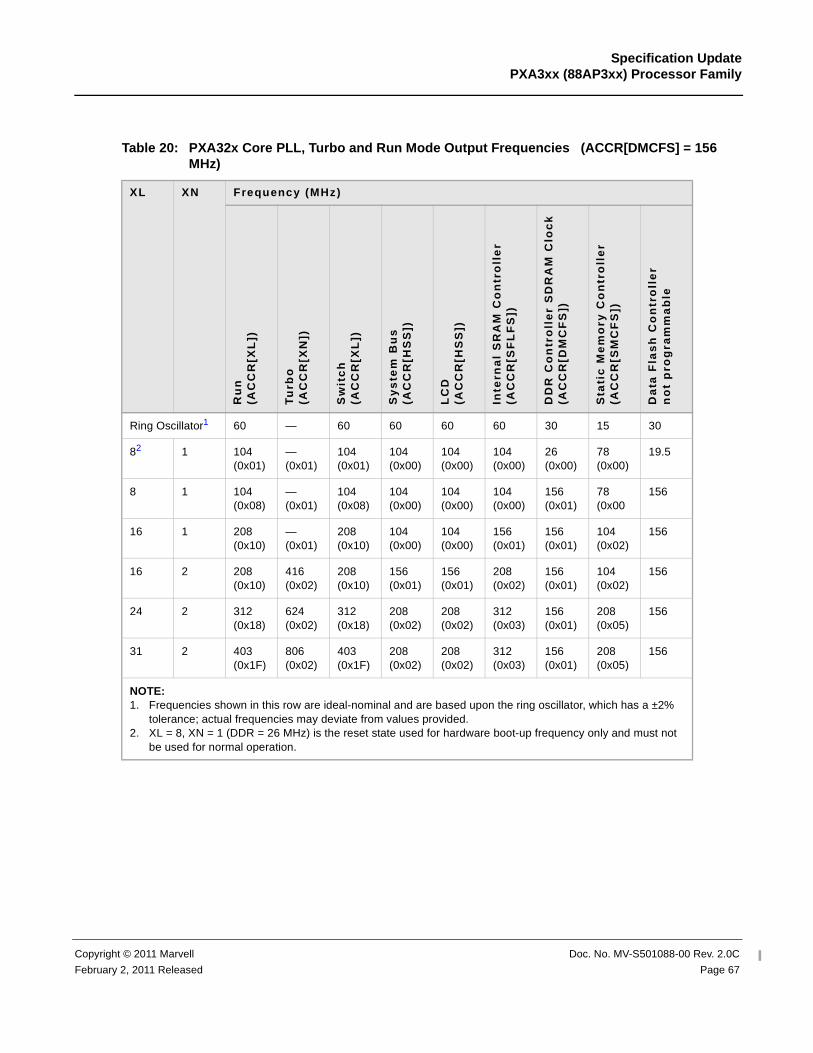
Copyright © 2011 Marvell Doc. No. MV-S501088-00 Rev. 2.0C
February 2, 2011 Released Page 67
Specification UpdatePXA3xx (88AP3xx) Processor Family
Table 20: PXA32x Core PLL, Turbo and Run Mode Output Frequencies (ACCR[DMCFS] = 156 MHz)
XL XN Frequency (MHz)
Ru
n
(AC
CR
[XL
])
Tu
rbo
(A
CC
R[X
N])
Sw
itc
h(A
CC
R[X
L])
Sy
ste
m B
us
(AC
CR
[HS
S])
LC
D(A
CC
R[H
SS
])
Inte
rna
l S
RA
M C
on
tro
lle
r(A
CC
R[S
FL
FS
])
DD
R C
on
tro
lle
r S
DR
AM
Clo
ck
(AC
CR
[DM
CF
S])
Sta
tic
Me
mo
ry C
on
tro
lle
r(A
CC
R[S
MC
FS
])
Da
ta F
las
h C
on
tro
lle
r n
ot
pro
gra
mm
ab
le
Ring Oscillator1 60 — 60 60 60 60 30 15 30
82 1 104 (0x01)
—(0x01)
104 (0x01)
104 (0x00)
104 (0x00)
104 (0x00)
26 (0x00)
78 (0x00)
19.5
8 1 104 (0x08)
— (0x01)
104 (0x08)
104 (0x00)
104 (0x00)
104 (0x00)
156 (0x01)
78 (0x00
156
16 1 208 (0x10)
— (0x01)
208 (0x10)
104 (0x00)
104 (0x00)
156 (0x01)
156 (0x01)
104 (0x02)
156
16 2 208 (0x10)
416 (0x02)
208 (0x10)
156 (0x01)
156 (0x01)
208 (0x02)
156 (0x01)
104 (0x02)
156
24 2 312 (0x18)
624 (0x02)
312 (0x18)
208 (0x02)
208 (0x02)
312 (0x03)
156 (0x01)
208 (0x05)
156
31 2 403 (0x1F)
806 (0x02)
403 (0x1F)
208 (0x02)
208 (0x02)
312 (0x03)
156 (0x01)
208 (0x05)
156
NOTE:1. Frequencies shown in this row are ideal-nominal and are based upon the ring oscillator, which has a ±2%
tolerance; actual frequencies may deviate from values provided.2. XL = 8, XN = 1 (DDR = 26 MHz) is the reset state used for hardware boot-up frequency only and must not
be used for normal operation.

Doc. No. MV-S501088-00 Rev. 2.0C Copyright © 2011 Marvell
Page 68 February 2, 2011 Released
Specification Update PXA3xx (88AP3xx) Processor Family
Table 21: PXA31x Core PLL, Turbo and Run Mode Output Frequencies (ACCR[DMCFS] = 156 MHz)
XL XN Frequency (MHz)
Ru
n
(AC
CR
[XL
])
Tu
rbo
(A
CC
R[X
N])
Sw
itc
h(A
CC
R[X
L])
Sy
ste
m B
us
(AC
CR
[HS
S])
LC
D(A
CC
R[H
SS
])
Inte
rna
l S
RA
M C
on
tro
lle
r(A
CC
R[S
FL
FS
])
DD
R C
on
tro
lle
r S
DR
AM
Clo
ck
(AC
CR
[DM
CF
S])
Sta
tic
Me
mo
ry C
on
tro
lle
r(A
CC
R[S
MC
FS
])
Da
ta F
las
h C
on
tro
lle
r n
ot
pro
gra
mm
ab
le
Vid
eo
Ac
ce
lera
tor
Un
it(A
CC
R[V
AU
F])
Ring Oscillator1 60 — 60 60 60 60 30 15 30 60
82 1 104 (0x01)
—(0x01)
104 (0x01)
104 (0x00)
104 (0x00)
104 (0x00)
26 (0x00)
78 (0x00)
19.5 104 (0x00)
8 1 104 (0x08)
— (0x01)
104 (0x08)
104 (0x00)
104 (0x00)
104 (0x00)
156 (0x01)
78 (0x00
156 78 (0x03)
16 1 208 (0x10)
— (0x01)
208 (0x10)
104 (0x00)
104 (0x00)
156 (0x01)
156 (0x01)
104 (0x02)
156 78 (0x03)
16 2 208 (0x10)
416 (0x02)
208 (0x10)
156 (0x01)
156 (0x01)
208 (0x02)
156 (0x01)
104 (0x02)
156 104 (0x00)
24 2 312 (0x18)
624 (0x02)
312 (0x18)
208 (0x02)
208 (0x02)
312 (0x03)
156 (0x01)
208 (0x05)
156 156(0x01)
24 2 312 (0x18)
624 (0x02)
312 (0x18)
312 (0x03)
312 (0x03)
312 (0x03)
156 (0x01)
208(0x05)
156 156(0x01)
31 2 312 (0x1F)
806 (0x02)
403 (0x18)
208 (0x02)
208 (0x02)
312 (0x03)
156 (0x01)
208(0x05)
156 156(0x01)
31 2 312 (0x1F)
806 (0x02)
403 (0x18)
312 (0x03)
312 (0x03)
312 (0x03)
156 (0x01)
208(0x05)
156 156(0x01)
NOTE:1. Frequencies shown in this row are ideal-nominal and are based upon the ring oscillator, which has a ±2%
tolerance; actual frequencies may deviate from values provided.2. XL = 8, XN = 1 (DDR = 26 MHz) is the reset state used for hardware boot-up frequency only and must not
be used for normal operation.

Copyright © 2011 Marvell Doc. No. MV-S501088-00 Rev. 2.0C
February 2, 2011 Released Page 69
Specification UpdatePXA3xx (88AP3xx) Processor Family
9.11 Changes(SCr#11) Type: Specification ChangeRelevant for: PXA32x and PXA31x ProcessorsRevision: PXA32x-C0, PXA31x-B1Errata BTS#: MLV-1872Description: The VCC_APPS and VCC_SRAM voltage levels for each operating point and power mode have de-
creased to improve power consumption.Changes: Refer to Table 22 for updated VCC_APPS and VCC_SRAM voltage specifications.
Table 22: Voltage, Temperature, and Frequency Electrical Specifications
Symbol Descript ion Min Typical Max Units
No
tes
VCC_APPS Voltage at Frequency Ranges (Turbo/Run/Switch/System Bus), (Power Mode (Sx/Dx/Cx))
Vccapps_0 Voltage applied on VCC_APPS S3/D4/C4 — 0 — V 2
Vccapps_1 Voltage applied on VCC_APPS at (S0/D0CS/Cx), (104/104/104/104), (208/208/208/104)
0.975 1 1.1 V 2
Vccapps_2 Voltage applied on VCC_APPS at (416/208/208/156) 1.05 1.10 1.2 V 2
Vccapps_3 Voltage applied on VCC_APPS at 624/312/312/208 1.188 1.25 1.35 V 2
Vccapps_3 Voltage applied on VCC_APPS at 624/312/312/312 1.42 1.45 1.475 V 2
Vccapps_3 Voltage applied on VCC_APPS in S0/D2/C2 or S0/D1/C2 1.05 1.10 1.2 V 2
Vccapps_4 Voltage applied on VCC_APPS at 806/403/403/208 1.235 1.30 1.4 V 2
Vccapps_4 Voltage applied on VCC_APPS at 806/403/403/312 1.42 1.45 1.475 V 2
Tpwrramp Ramp Rate 2.00 10.00 12.00 mV/μs 6
VCC_SRAM Voltage at Frequency Range (Turbo/Run/Switch/System Bus), (Power Mode (Sx/Dx/Cx) @ SRAM frequency)
Vccsram_0 Voltage applied on VCC_SRAM S3/D4/C4 — 0 — V 2
Vccsram_1 Voltage applied on VCC_SRAM at (S0/D0CS/Cx), (104/104/104/104), (208/208/208/104)
0.975 1 1.1 V 2
Vccsram_2 Voltage applied on VCC_SRAM at (416/208/208/156) 1.05 1.10 1.2 V 2
Vccsram_3 Voltage applied on VCC_SRAM at 624/312/312/208 1.188 1.25 1.35 V 2
Vccsram_3 Voltage applied on VCC_SRAM at 624/312/312/312 1.42 1.45 1.475 V 2
Vccsram_3 Voltage applied on VCC_SRAM in S0/D2/C2 or S0/D1/C2 1.05 1.10 1.2 V 2
Vccsram_4 Voltage applied on VCC_SRAM at 806/403/403/208 1.235 1.30 1.4 V 2

Doc. No. MV-S501088-00 Rev. 2.0C Copyright © 2011 Marvell
Page 70 February 2, 2011 Released
Specification Update PXA3xx (88AP3xx) Processor Family
Vccsram_4 Voltage applied on VCC_SRAM at 806/403/403/312 1.42 1.45 1.475 V 2
Tpwrramp Ramp Rate 2.00 10.00 12.00 mV/μs 6
NOTE:1. System design must ensure that the device case temperature is maintained within the specified limits. In some system
applications it may be necessary to use external thermal management (for example, a package-mounted heat spreader) or configure the device to limit power consumption and maintain acceptable case temperatures.
2. The voltage ranges specified for VCC_APPS and VCC_SRAM are the targeted voltage ranges for the product. These ranges may extend or narrow depending on actual product performance and product skews. Marvell recommends that extended voltage and current capabilities be designed into the power management IC to accommodate future changes to this specification without requiring changes to the power management IC.
3. VCC_MVT requires the capability to increase from the normal operating voltage of 1.8 V to 1.9 V during certain times. This increased voltage is required under certain conditions, not during normal operation. When VCC_MVT is raised to 1.9 V, it is operating in “boost mode”. Boost mode is only used during factory programming. If VCC_PLL, VCC_OSC13M and VCC_BG are supplied by the same PMIC supply, which is the method Marvell recommends, these other voltages also operate at 1.9 V. Maximum current capabilities and voltage tolerances are identical in boost mode and normal operation.
4. This option allows one or more 128 Kbyte SRAM banks to retain state during S2/D3/C4 mode.5. Reset voltage for VCC_APPS and VCC_SRAM is 1.4 V and the startup frequency is 104/104/104/104 MHz.6. Min ramp rate = (Maximum voltage transition) / (LPM_DEL - ((Power I2C command execution time))
Table 22: Voltage, Temperature, and Frequency Electrical Specifications (Continued)
Symbol Description Min Typical Max Units
No
tes

Copyright © 2011 Marvell Doc. No. MV-S501088-00 Rev. 2.0C
February 2, 2011 Released Page 71
Specification UpdatePXA3xx (88AP3xx) Processor Family
10. Documentation Changes Summary
Table 23: Summary of Documentation Changes
Number Description Document Relevant Revis ion
Revision Fixed
11.1 Changes(SCr#1)
PCLK_STALL bit description missing from bit 28 of the LCD Controller Control Register 3 (LCCR3).
PXA3xx Processor Family Vol. II: Memory Controller Configuration Developers Manual
2.0 Next Revision
11.2 Changes(SCr#2)
HCOFF2 and HCOFF3 registers are missing from the DDR_HCAL register.
PXA3xx Processor Family Vol. II: Memory Controller Configuration Developers Manual
2.0 Next Revision

Doc. No. MV-S501088-00 Rev. 2.0C Copyright © 2011 Marvell
Page 72 February 2, 2011 Released
Specification Update PXA3xx (88AP3xx) Processor Family
11. Detailed Descriptions for Documentation Changes
11.1 Changes(SCr#1)Type: Documentation ChangeRelevant for: PXA3xx Processor Family Vol. II: Memory Controller Configuration Developers ManualRevision: 2.0Fixed In: Next RevisionErrata BTS#: MP-6478Description: PCLK_STALL bit description missing from bit 28 of the LCD Controller Control Register 3 (LCCR3).Changes: The LCCR3 register has been updated as shown in Table 25.
Current Documentation:
Table 24: LCCR3 Bit Definitions
Physical Address0x4400_000C
LCCR3 LCD Control ler
User Settings
Bit 31 30 29 28 27 26 25 24 23 22 21 20 19 18 17 16 15 14 13 12 11 10 9 8 7 6 5 4 3 2 1 0
PD
FO
R
BP
P3
Re
se
rve
d
DP
C
BPP
OE
P
PC
P
HS
P
VS
P
API ACB PCD
Reset 0 0 0 ? 0 0 0 0 0 0 0 0 0 0 0 0 0 0 0 0 0 0 0 0 0 0 0 0 0 0 0 0
Bits Access Name Description
28 — — NOTE: Reserved

Copyright © 2011 Marvell Doc. No. MV-S501088-00 Rev. 2.0C
February 2, 2011 Released Page 73
Specification UpdatePXA3xx (88AP3xx) Processor Family
Updated Documentation:
Table 25: LCCR3 Bit Definitions
Physical Address0x4400_000C
LCCR3 LCD Control ler
User Settings
Bit 31 30 29 28 27 26 25 24 23 22 21 20 19 18 17 16 15 14 13 12 11 10 9 8 7 6 5 4 3 2 1 0
PD
FO
R
BP
P3
PC
LK
_S
TA
LL
DP
C
BPP
OE
P
PC
P
HS
P
VS
P
API ACB PCD
Reset 0 0 0 ? 0 0 0 0 0 0 0 0 0 0 0 0 0 0 0 0 0 0 0 0 0 0 0 0 0 0 0 0
Bits Access Name Descript ion
28 R/W PCLK_STALL PCLK StallStalls the PCLK while the output FIFOs are under-running.0 = Pixel clock keeps running when output FIFO underruns. The
pixel data sent out during this time is the last valid pixel.1 = Pixel clock stalls when the FIFO under-runs. The pixel data
sent out during this time is the last valid pixel.NOTE: 1. Use this bit when using larger display resolutions where
artifacts appear on the screen caused by FIFO underruns.2. This bit is ignored for smart panels3. Stalling PCLK may violate timing specifications for the panel. Ensure that all panel timing requirements are being met when the FIFO underruns occur and PCLK is stalled.

Doc. No. MV-S501088-00 Rev. 2.0C Copyright © 2011 Marvell
Page 74 February 2, 2011 Released
Specification Update PXA3xx (88AP3xx) Processor Family
11.2 Changes(SCr#2)Type: Documentation ChangeRelevant for: PXA3xx Processor Family Vol. II: Memory Controller Configuration Developers ManualRevision: 2.0Fixed In: Next RevisionErrata BTS#: MP-6479Description: HCOFF2 and HCOFF3 registers are missing from the DDR_HCAL register.Changes: Refer to Table 26 for bit definitions locations for HCOFF3 and HCOFF2.
Table 26: DDR_HCAL Bit Definitions
Physical Address0x4810_0060
DDR_HCAL Dynamic Memory Controller
User Settings
Bit 31 30 29 28 27 26 25 24 23 22 21 20 19 18 17 16 15 14 13 12 11 10 9 8 7 6 5 4 3 2 1 0
HC
EN
res
erv
ed
res
erv
ed
HC
PR
OG
SE
TA
LW
AY
S
reserved
HCOFF3 HCOFF2 HCOFF1 HCOFF0
res
erv
ed
HCRNG
Reset 0 ? 0 0 1 0 0 0 ? ? 0 0 0 0 0 0 0 0 0 0 0 0 0 0 0 0 ? 0 0 0 0 0
Bits Access Name Descript ion
21:18 R/W HCOFF3
Hardware Calibration Offset for DQS[3]:
Provides a fractional offset from the value determined by the hardware calibration circuit. The offset range is 1/8 to 15/8 of a DDR data eye. The value programmed into delay line is DQS[3] = (DDR_DMCISR[ORV]) * HCOFF3. For a derivation of this formula, see Section 13.10.1.4.
0b0000 = 0 - No offset (strobe centered)
0b0001 to 0b0111= 1/8 to 7/8 - Offset (moves strobe left of center)
0b1000 = 8/8 - No offset (strobe centered)
0b1001 to 0b1111 = 9/8 to 15/8 - Offset (moves strobe right of center)
17:14 R/W HCOFF2
Hardware Calibration Offset for DQS[2]:
Provides a fractional offset from the value determined by the hardware calibration circuit. The offset range is 1/8 to 15/8 of a DDR data eye. The value programmed into delay line is DQS[2] = (DDR_DMCISR[ORV]) * HCOFF2. For a derivation of this formula, see Section 13.10.1.4.
0b0000 = 0 - No offset (strobe centered)
0b0001 to 0b0111= 1/8 to 7/8 - Offset (moves strobe left of center)
0b1000 = 8/8 - No offset (strobe centered)
0b1001 to 0b1111 = 9/8 to 15/8 - Offset (moves strobe right of center)

DisclaimerNo part of this document may be reproduced or transmitted in any form or by any means, electronic or mechanical, including photocopying and recording, for any purpose, without the express written permission of Marvell. Marvell retains the right to make changes to this document at any time, without notice. Marvell makes no warranty of any kind, expressed or implied, with regard to any information contained in this document, including, but not limited to, the implied warranties of merchantability or fitness for any particular purpose. Further, Marvell does not warrant the accuracy or completeness of the information, text, graphics, or other items contained within this document. Marvell products are not designed for use in life-support equipment or applications that would cause a life-threatening situation if any such products failed. Do not use Marvell products in these types of equipment or applications. With respect to the products described herein, the user or recipient, in the absence of appropriate U.S. government authorization, agrees: 1) Not to re-export or release any such information consisting of technology, software or source code controlled for national security reasons by the U.S. Export Control Regulations ("EAR"), to a national of EAR Country Groups D:1 or E:2; 2) Not to export the direct product of such technology or such software, to EAR Country Groups D:1 or E:2, if such technology or software and direct products thereof are controlled for national security reasons by the EAR; and, 3) In the case of technology controlled for national security reasons under the EAR where the direct product of the technology is a complete plant or component of a plant, not to export to EAR Country Groups D:1 or E:2 the direct product of the plant or major component thereof, if such direct product is controlled for national security reasons by the EAR, or is subject to controls under the U.S. Munitions List ("USML"). At all times hereunder, the recipient of any such information agrees that they shall be deemed to have manually signed this document in connection with their receipt of any such information. Copyright © 2011. Marvell International Ltd. All rights reserved. Marvell, the Marvell logo, Moving Forward Faster, Alaska, Fastwriter, Datacom Systems on Silicon, Libertas, Link Street, NetGX, PHYAdvantage, Prestera, Raising The Technology Bar, The Technology Within, Virtual Cable Tester, and Yukon are registered trademarks of Marvell. Ants, AnyVoltage, Discovery, DSP Switcher, Feroceon, GalNet, GalTis, Horizon, Marvell Makes It All Possible, RADLAN, UniMAC, and VCT are trademarks of Marvell. All other trademarks are the property of their respective owners.Marvell Semiconductor, Inc.5488 Marvell LaneSanta Clara, CA 95054, USATel: 1.408.222.2500Fax: 1.408.752.9028Email: [email protected]
Specification Update PXA3xx (88AP3xx) Processor Family
Doc. No. MV-S501088-00 Rev. 2.0C Copyright © 2011 Marvell
Page 75 February 2, 2011, Released