Embed Size (px)
Citation preview

Corso di Dottorato di ricerca
in Scienze Ambientali ciclo XXXI
Tesi di Ricerca
From Dye Sensitized to Perovskite Solar Cells:
processes and materials for the forthcoming era of
Photovoltaic technology
Settore Scientifico Disciplinare: Fisica sperimentale,
FIS/01
Coordinatore del Dottorato
Professore Bruno Pavoni
Supervisore
Professore Francesco Gonella
Co-tutori di tesi
Professore Giuseppe Calogero
Dottoranda Jessica Barichello Matricola 829851

Abstract
In the context of the serious environmental issues, that Earth is facing, among which atmospheric
CO2 increase is a crucial one, implementation of clean technologies is mandatory. The present
PhD thesis concerns the study of two new third-generation PV technologies: Dye Sensitized Solar
Cells (DSSCs) and Perovskite Solar Cells (PSCs). A typical DSSC is a low cost device of easy
fabrication, widely investigated for indoor application, where the dye is used to collect light. In
the former study, the research focused on natural dye extraction and the electrolyte optimization in
the cell in accordance with a natural pigment. I realized and presented, for the first time in
literature, a natural dye-based solar module of 8.7 cm2 with 1 % of power conversion efficiency
(PCE), stable for 1000 hours. A PSC is a kind of solar cell that includes a perovskite-structured
compound, most commonly a hybrid organic-inorganic lead halide-based material, as the light-
harvesting active layer. Unlike DSSC, in PSC the liquid electrolyte has been replaced by a solid-
state hole transport material (HTM), and since 2009 the run for boosting the PCE of PSC has
started. In the latter study, the research focuses therefore on the optimization of an easy and low-
cost PSC structure with a carbon layer replacing the HTM and gold usually used in a conventional
high efficiency PSC. Despite all controversial studies on how moisture badly affects perovskite, it
has been observed a beneficial water effect on the perovskite growth and formation in a 2-step
deposition, which enhances the PCE of 16 % with respect to the non-treated cell.

Table of contents
Introduction………………………………………………………………………………1
References....…………………………….………………………………………………..9
Chapter 1 –Theoretical background and state of art…………………………………10
1.1 Basic principles on photochemistry and on photo-physics applied to
photovoltaic…………………………………………………………………………10
1.1.1 Solar Spectrum…………………………………………………………………..10
1.1.2 Light absorption………………………………………………………………… 13
1.1.3 Fate of the excited state…………………………………………………………. 14
1.1.4 Photovoltaic conversion…………………………………………………………16
1.2 Dye-Sensitized Solar Cell………………………………………………………18
1.2.1 DSSC Architecture………………………………………………………………18
1.2.2 Working principles………………………………………………………………22
1.2.3 Photovoltaic Parameters…………………………………………………………23
1.3 Perovskite Solar Cell…………………………………………………………....28
1.3.1 PSC Architecture………………………………………………………………...28
1.3.2 Working principles………………………………………………………………34
1.3.3 Photovoltaic Performances………………………………………………………35
References……………………………………………………………………………….37
Chapter 2 – Instrumental setup and device fabrication………………………………47
2.1 DSSC fabrication………………………………………………………………....... 47
2.1.1 Anode ………………………………………………………………………………47
2.1.2 Cathode fabrication…………………………………………………………………48
2.1.3 Electrolyte…………………………………………………………………………..48
2.1.4 DSS Module fabrication……………………………………………………………48
2.1.5 Photoanode Characterization……………………………………………………….49
2.2 Carbon based PSC fabrication…………………………………………………......50
2.2.1 Planar carbon based PSC Fabrication……………………………………………….51

2.2.2 Characterization of Perovskite Solar Cells…………………………………………52
References………………………………………………………………………………53
Chapter 3 – Natural dyes and extraction……………………………………………...55
3.1 Natural dyes…………………………………………………………………….55
3.1.1 Molecular structure of chlorophylls and historical background…………………55
3.1.2 Molecular structure of carotenoids………………………………………………61
3.2 Extraction and preparation of solutions………………………………………63
References……………………………………………………………………………….65
Chapter 4- Carbon based Perovskite Solar Cell……………………………………...68
4.1- Carbon based Perovskite Solar Cell………………………………………………68
4.2- Carbon based-Planar Perovskite Solar Cell……………………………………...72
References……………………………………………………………………………….74
Chapter 5 – Dye Sensitized Solar Cells- Results and Discussions……………….......80
5.1 Characterization and study of Chlorophylls as natural sensitizers……………..80
5.1.1 Optical properties and extraction………………………………………………..80
5.1.2 Photovoltaic characterization of DSSC………………………………………….85
5.1.3 Conclusion………………………………………………………………………86
5.2 Characterization and study of carotenoids as sensitizers…………………....87
5.2.1 Optical properties and extractions……………………………………………….87
5.2.2 Photoelectrochemical characterization of DSSCs……………………………….89
5.2.3 Scaling up from DSC to DSM……………………………………………………..94
5.2.4 Conclusion……………………………………………………………………………………………………….96
References………………………………………………………………………………97
Chapter 6 Carbon based Perovskite Solar Cells- Result and Discussion………….101
6.1 Characterization and study of the device optimization……………………........101
6.1.2 Characterization and study on the water effect…………………………………...105

6.1.3 Conclusion………………………………………………………………………...113
6.2 Carbon based module...............................................................................................113
6.3 Characterization and study on carbon planar devices...........................................116
References……………………………………………………………………………...118
Conclusion……………………………………………………………………………...121
Publications…………………………………………………………………………….124
PhD Schools and curses……………………………………………………………….127
Project………………………………………………………………………………….127
Many Thanks..................................................................................................................128

1
Introduction
In the addressing of the environmental problems, with particular reference to the
need for exploiting renewable and clean energy sources within a global society
debate, many significant variables have to be taken into account. The environment
problem, although appeared only recently in the agenda of global governance,
manifests itself with increasing strength. The idea that an anthropic intervention
could damage beyond any possibility of repair climate and environmental
conditions for the entire planet took place only after the end of World War II. This
occurs after the launch, in August 1945, of the first two atomic bombs, along with
the increasing awareness about the long-lasting damages after their explosion. The
problem of the conservation and safeguarding of the environment, although
confined in scope for much of studies and reports, without an actual feedback in
terms of environmental policies, would have grown from that precise historical
moment. Along with this scientific awareness, environmental issues then entered
global debate also in terms of ethical, economic, political and social choices. In
this framework, the research on solar technologies embraces several different
aspects, and is pursued following a variety of different approaches. In particular,
in the perspective addressed by the very concept of integrated sustainability,
research groups are active in all the aspects expected to give a contribution for
meeting the demand of a transition towards a world based on renewable energy
sources, reflecting the three pillars of integrated sustainability, namely,
environmental, social and economic. More recently, starting from Kyoto Protocol
in 1997, climate change issues pushed forward towards an integrated energy and
climate change strategy. In this respect, the European Union set ambitious targets
for 2020, aimed at addressing the right track towards a sustainable future by

2
developing a low-carbon economy based on energy efficiency. In particular, the
so-called "20-20-20 strategy" forms the goal basis for the actions, to:
• reduce greenhouse gases of 20%;
• reduce energy consumption by 20% through increased energy efficiency;
• meet the 20% of our energy needs through the use of renewable energy.
Besides the greenhouse gases emissions from the industrial system or due to the
energy production process itself, attention is also payed to the emissions of air
pollutants caused by motorized transport and domestic heating/cooling. On these
fronts, research has made significant progress towards suitable technologies able
to reduce the impact of these factors that can be defined as "private". However, as
far as in most cases any investment is seen only from the economic point of view,
the environmental issues will require specific policies to be effectively addressed.
On all technological fields considered in recent years (wind, biomass, solar,
hydroelectric, geothermal, etc.), we had many important innovations that could
renovate the energy industry. Among all the possibilities the market offers, it is
fair to say that the solar energy is certainly the most easily exploitable, given that
it strikes us daily and directly for many hours. This de facto inexhaustibility
distinguishes the photovoltaics from most other energy sources. The photovoltaic
energy is already proving a great capacity for development.
Solar PV technology is expected to play a major role also in integrated hybrid
energy production plants, as well as in supplying energy in peculiar geographical
or logistic situations that require specific planning. This makes any
comprehensive study on the sustainability of PV technology even more complex.
The need for an integration of all the aspects of sustainability requires a series of
compromises, so that researchers have always to take into account the feasibility

3
and the viability of their research output in an application perspective that should
extend beyond the engineering aspect, even if the latter may be regarded as a pre-
requisite for any application purpose.
Presently, it has become more and more generally accepted the idea that a push
towards the incentive policies on products related to the green industry -and in
special way to renewable sources of energy- may be effectively coupled with the
economic development in many respects. From a microeconomic point of view,
more in touch with the needs of the citizen and of the enterprise, the green boom
has witnessed many families adopted the photovoltaic energy source. PV plants
are usually of 2.8 kW, more than the cost to cover the energy needs of an average
family, and their installation was supported in Italy by the strong incentives
"Conto Energia".
The 2018 global status report for renewables presented remarkable results [1].
2017 was a record year for renewable energies but particularly for solar PV that
raises enormously for power capacity production respect with the previous year,
fig. 1 and 2. Solar PV increased the power capacity more than any other power
generating technologies. The total PV installation in 2017 overcame the net
capacity additions of combined fossil fuels and nuclear energy. In numerous main
markets, such as China, India, Japan and United States, the solar PV resulted the
major font of new power capacity. It was estimated that, in each hour of the year,
40.000 panels were installed. This great boost was mainly obtained by China’s PV
installation that increased of the 50% with respect to 2016; indeed China surprised
adding more PV capacity (53.1 GW) than the entire world in 2015 (51 GW). For
the first time, PV was the Chinese leader source for new power capacity. The PV
market is mainly concentrated in few countries but last data reveal that more
countries are emerging for contributing to the global growth; indeed, by the end of

4
2017, every continent at least installed 1 GW or more of capacity. Germany,
Japan, Belgium, Italy and Australia are the leaders for PV capacity for inhabitants.
And, China, United States, Japan, Germany and Italy are the top countries for
cumulative capacity. Significant percentages reveal that, in 2017, the PV met the
electricity demand of several countries such as 8.7% in Italy, 7.6% in Greece, 7%
in Germany and 5.7% in Japan. By the end of 2017, PV contributed to the annual
electricity request with the 2% at least in 22 countries, including China and India.
Figure 1. Solar PV global capacity trend from 2007 to 2017. Data are presented in direct
current (DC). Adapted image from Renewables Status Report 2018. p 91 and
https://www.lifegate.it/persone/stile-di-vita/panda-solare-cresce-potenza-installata [2]. PV
solar plant with a Panda shape realized in Hong Kong by Panda Green Energy Group.

5
Figure 2. Top ten countries of the world for annual additions. Data are presented in direct
current (dc). Adapted image from Renewables Status Report 2018. p 91 and
https://www.lifegate.it/persone/stile-di-vita/panda-solare-cresce-potenza-installata [2]. PV
solar plant with a Panda shape realized in Hong Kong by Panda Green Energy Group.
Positive answers derived also from continues efforts to improve the recycling
processes of the used materials in panels [1]. The first practical example is the
First Solar, a PV thin film manufacturer that is designing its panels to facilitate a
materials recycle process while the RCS refining, an electronics recyclers
company, is advancing its competences in recycling PV panels. Veolia, an
environmental service provider in France, is planning to build a solar module
recycling facility.
Photovoltaic (PV) solar energy conversion has the potential to play a major role in
future electricity generation.
Since 1954, when the first PV device was invented by three scientists, Gerald
Pearson, Calvin Fuller and Daryl Chapin, at the Bell Telephone Laboratories

6
(New Jersey, USA), and obtained the first power conversion efficiency of 6%,
scientists and researchers have been dedicated to optimize the device. Numerous
studies until today focus on the device engineering, discovering the most
sustainable materials and system operation in order to meet the requested three
pillars in PV field: power conversion efficiency, stability and cost in both
economic and environmental terms. Since the beginning of 1950, many
technologies has been developed and are gathered in three generation depending
on the utilized materials. In the course of the last decade, photovoltaic technology
has undergone a strong innovation. Like all technologies, even those that are
applied to the solar field, will vary over time to adapt to the demands that the
market requires and leveraging innovations. The solar industry has now arrived at
the third generation, but the panels currently present on the market are the second.
The most currently installed PV arrays consist of crystalline or polycrystalline
silicon; in second-generation thin-film architectures, light is absorbed and charge
generated in a solid layer of this semiconductor. Regardless of semiconductor,
thin-films offer prospects for a major reduction in material costs by eliminating
the silicon wafer. Thin films also offer other advantages, particularly the increase
in the unit of manufacturing from a silicon wafer (100 cm2) to a glass sheet (1m2),
about 100 times larger. The Carnot limit on the conversion of sunlight to
electricity is 95 % as opposed to the theoretical upper limit of 33 % for a standard
solar cell [3]. This suggests the performance of solar cells could be improved 2–3
times if different concepts would be used to produce a ‘third generation’ of high-
performance, low-cost photovoltaic products. Some of the most promising
emerging technologies for ultimate low-cost manufacture are solution-processed,
such as organic photovoltaics (OPV), dye-sensitized solar cells (DSSCs), and
semiconductor-sensitized or extremely thin absorber solar cells [4, 5]. In figure 3,

7
it is shown the global trend in terms of power conversion efficiency from 1975
until now for each studied PV technology [6].
Even research on technologies that for the moment appear as less promising from
the engineering point of view, as may be the case of DSSC, is therefore addressed
along with more appealing technological options.
The current studies about PV technology are so rapidly evolving that it is difficult
even to define a well-assessed framework. The research is in fact focused time to
time in separated single aspect which each study field is related with.
A comprehensive evaluation of the feasibility of PV technology is in fact
mandatory within an integrated sustainability framework, where environmental,
social and economic issues are to be all taken into account for an effective energy
planning.
Updated articles and reviews may be found concerned with basic research and
understanding, high-efficiency PV technology [7], eco-friendly PV technology
[8], PV energy network integration, economic issues, LCA-based perspectives
(and so impacts, disposal, etc.), and a miscellaneous of different issues among
which are the different spatial and temporal scales of PV use, its site dependency,
and in general its viability within concepts like circular economy integration or
smart cities [9, 10, 11].
Concerning the innovative materials for PV cells technology, the presented
research is then placed in the multi-aspect field of high-efficient materials, eco-
friendly materials and low-cost materials.
These studies regards two of the main technologies of the third generation that in
the last 10 years has attracted wide interest: Dye Sensitized Solar Cell and
Perovskite Solar Cell.

8
Figure 3. Performance trend of PV technologies since 1975 until July 2018. https://www.nrel.gov/pv/assets/images/efficiency-chart.png. Last access 28/09/2018

9
References
[1] Ren21. Reneweables 2018 Global status report. 90-10.
[2] Adapted image of a PV plant with a Panda shape. Lifegate.
https://www.lifegate.it/persone/stile-di-vita/panda-solare-cresce-potenza installata.
Last access 1/10/2018.
[3] W. Shockley, H. J. Queisser, Detailed Balance Limit of Efficiency of p-n
Junction Solar Cells. J. Appl. Phys. 32, 510 (1961).
[4] S. D. Stranks, G. E. Eperon, G. Grancini, C. Menelaou, M. J. P. Electron-Hole
Diffusion Lengths Exceeding 1 Micrometer in an Organometal Trihalide
Perovskite Absorber. Science, 342, (2013), 6156, 341-344.
[5] G. Conibber, Third generation photovoltaics, Materialstoday, 10, 2007, 11
[6] https://www.nrel.gov/pv/assets/images/efficiency-chart.png.
[7] B. Parida, S. Iniyan, R. Goic. A review of solar photovoltaic technologies.
Renewable and Sustainable Energy Reviews. 15, Issue 3, (2011), Pages 1625-
1636.
[8] G. Calogero, A. Bartolotta, G. Di Marco, A. Di Carlo, F. Bonaccorso.
Vegetable-based dye-sensitized solar cells Chem. Soc. Rev., 44, (2015), 3244–94.
[9] S. Mekhilef, R. Saidur, M. Kamalisarvestani, Effect of dust, humidity and air
velocity on efficiency of photovoltaic cellsRenewable and Sustainable Energy
Reviews, 16, 5, (2012), 2920-2925.
[10] N. Espinosa, M. Hösel, D. Angmo, Fr. C. Krebs, Solar cells with one-day energy
payback for the factories of the future. Energy Environ. Sci., 5, (2012), 5117-5132.
[11] R. Laleman, J. Albrecht, J. Dewulf, Life Cycle Analysis to estimate the
environmental impact of residential photovoltaic systems in regions with a low
solar irradiation, Renew. Sust. Energ. Rev., 15, 1, (2011), 267-281.

10
Chapter 1 –Theoretical background and state of art
In this chapter, I review the solar energy characteristics and the effect of light
when it reaches materials on the Earth. Later, I introduce the two PV technologies
that I treated in my research activities: DSSC and PSC.
1.1 Basic principles on photochemistry and on photo-physics applied to
photovoltaic
1.1.1 Solar Spectrum
The Earth receives from the Sun in one hour the amount of energy that the
humanity consumes in an entire year [1].
Part of this energy is reflected directly, part is absorbed by the oceans and the
atmosphere contributing to the winds and currents, part is absorbed by the soil and
then partly reflected, a small amount is even used for photosynthesis. On solar
power depends almost all the energy that is present on our planet (other than
geothermal phenomena, nuclear ones and those due to gravity and the Lunar
motions, etc.).
The power emitted by the Sun is calculated from the famous Stefan-Boltzman
equation: P= σ T4 where σ is the Stefan-Boltzman constant and T is the surface
temperature of the sun. Now, how can we calculate the amount of solar energy
that reaches the Earth? Simply, we have to calculate the solar constant of the Earth
that is the ratio between the total power emitted by the Sun and the area of the
sphere on which the Earth orbits. So = P/(4 π r2) where r is the Earth-Sun distance.
Each planet has its solar constant, for the Earth it is approximately 1370 W/m2, it
is a key parameter for the calculation of the incident solar power per unit area at
any point of the Earth. Considering the effect of the atmosphere, it decreases to
circa 947 W/m2, which become 1042 W/m2 if the component of light scattered

11
from the atmosphere is also taken into account. However, the incident power is
influenced also by the declination of the Sun, the angle it forms with the vertical.
The declination effect manifests itself in two ways. First, the greatest the
variation, the greatest the thickness of the layer of air traversed by the light before
reaching Earth. This effect is a schematic drawing with a parameter called Air
Mass (AM), which quantifies this thickness in number of equivalent atmospheres.
The solar spectrum AM 0 is what there is outside of the atmosphere, the spectra
AM 1 is for the Sun at the zenith. In other situations, there is: AM=1/cosα, where
α is the angle of declination (es. AM 1.5 is 48.2°). The intensity of light at the
surface, in a plane perpendicular to the direction of the Sun's rays, therefore
depends on the angle of declination (Fig. 1.1).
Light is an electromagnetic radiation that propagates at the speed of 3*108 m/s.
We can image light with a wave shape, with three main features: the wavelength,
λ, the frequency, v, and the amplitude. The solar radiation is composed by photons
that transport a quantum of energy, E=hv, where h is the Plank constant and v is
the frequency of the wave. Wavelengths that depend on frequency, v, following
this equation λ= v/ v where v is the wave propagation speed, are associated with
the carried energy by individual quanta: the ultraviolet and gamma rays, very
energetic, have very short wavelengths; infrared rays and radio waves are not very
energetic with long wavelengths. The intermediate wavelengths correspond to the
visible electromagnetic radiation to the human eye, the light; the range is from
400 nm of violet color to 700 nm of red one. The wavelength mix constitutes the
solar radiation and the amount of each makes it appears white. When solar
radiations go through atmosphere, it may be absorbed or scattered due to impacts
with molecules as water vapor, and aerosols. Then, phenomena attenuate

12
wavelengths and the resulting electromagnetic spectrum assumes an irregular
profile [Fig. 1.2].
Figure 1.1 Sun declination at AM0 0, AM 1, AM 1.5 and AM 2. Adapted image from the web site LaserFocusWorld: https://www.laserfocusworld.com/articles/2009/05/photovoltaics-measuring-the-sun.html. [2]
Figure 1.2 Solar Spectrum of the ideal black body, of the extraterrestrial solar radiation and of the terrestrial solar radiation. Adapted image taken from Global Change magazine for Schools. http://klimat.czn.uj.edu.pl/enid/Climate_Change_classes_ss/ss_Energy_from_the_Sun_6ev.html [3]
AM 0 is what there is outside the atmosphere
Air Mass (AM) quantifies in number of equivalent atmospheres
Ideal black body (temperature 5900K)
Extraterrestrial solar radiation (air mass
AM0)

13
1.1.2 Light absorption
When light strikes an object, its electromagnetic radiation interacts with the object
material. Object material can absorb, reflect or transmit the solar radiation; this
depends on the chemistry of the material. The light absorption is the ability of the
material to absorb the electromagnetic radiation energy that propagates within it.
Electrons receive the photo-energy from the light that promotes them from a
lower to a higher energy level. The light absorbance depends on the nature of the
material and on frequency of the incident light. The absorption of light can be
used to know the material properties: its absorption spectrum indicates the
frequencies that are absorbed and allows the identification of the atoms and
molecules that compose it. Electrons in atoms and molecules tend to vibrate at
their own natural frequency. When a light wave of a certain frequency hits an
atom or a molecule with vibrational electrons at the same frequency, those
electrons create a vibrational motion and convert the vibrational energy in thermal
energy. The light absorption by a material can occur when the frequency of the
light matches with the vibrational frequency of material atoms (1). Due to each
materials is composed by different atoms or molecules with its own characteristic
frequency motions, different light frequency are absorbed selectively from each
materials.
A +hv -> A* (1)
A* represents the excited-state of the molecula (A) when a photon (hv) interacts
with it; A* must be considered as a new chemical species with its own chemical-
physical proprieties different from A.
When a photon, with appropriate energy, is absorbed by a molecule, it can
promote an electron from a starting level (S0) to an higher one (S1, S2, S3..);
specifically, the energy gap between the starting level and the arrival level of the

14
excited electron must match with the energy of the absorbed photon. As seen
before, the energy of a photon, E, is correlated to its wavelength and it is
described by the formula: E= hc/λ. Therefore, a molecule can absorb light only at
the specific wavelengths corresponding to the possible transition in the same
molecule. The lowest amount of energy that can be absorbed corresponds to the
gap between the Highest Occupied Molecular Orbital (HOMO) level and the
Lowest Unoccupied Molecular orbital (LUMO) level of the molecule. Depending
on its energy, electrons can be excited to a higher orbital, thus being possible
different singlet excitation states S1, S2, S3.
The Lambert-Beer law describes the absorption of electromagnetic radiations and
it is used for the application in spectrophotometry techniques. The absorption is
directly proportional to the concentration of the solution in the cuvette, indeed, A=
ɛ l C, where ɛ is the molar absorption coefficient, l is the optical path so the
thickness that light goes through and C is the solution concentration.
1.1.3 Fate of the excited state
When an electron is photo-excited by a wavelength, different events may appear
and these are shown in the energetic diagram of Jablonski (Fig. 1.3). An
explanation of each pathways of energy dissipation, after an electron acceptance is
following. In the vertical axis of the diagram, there is the energy and the diagram
is divided into 3 columns where each event is drawn. [4, 5].
Absorbance: the first transition in a Jablonski diagram is the absorption of
electrons and straight arrows pointing up represent this (Fig. 1.3). As previously
said, absorbance is a transition where an electron is promoted from a lower to a
higher energy level after harvesting a wavelength. Absorption is a fast transition
that occurs around 10-15 s.

15
Vibrational relaxation and Internal Conversion (IC): when a molecule is excited to
a higher energy level than the first electronic state, the vibrational relaxation
brings the excited molecule towards the vibrational level 0 of the singlet state S1
with a time of 10 -13-10-11 seconds. This process takes place between vibrational
levels of the same electronic state and the dotted arrow pointing down represents
it (Fig. 1.3). The internal conversion is equal to the vibrational relaxation with the
only exception that IC occurs when an excited electron dissipate from a
vibrational level in a higher electronic state (S2) to a lower one (S1).
Fluorescence: this process consists of a photon emission with the decay from S1 to
S0. A straight arrow pointed down represents the fluorescence pathway that occurs
between 10-9 to 10-7 s (Fig. 1.3). The emitted photon energy is lower than that one
of the excited electron due to vibrational relaxation and internal conversion
processes dissipate energy away from the electron.
Intersystem crossing: it is a non-radiative transition from an excited singlet
electronic state (S1) to a triplet one (T1). This is the lowest process in the Jablonski
diagram around 10-3 s. The horizontal dotted arrow from the second column to the
third one in figure 1.3 represents this.
Phosphorescence: The phosphorescence spectra is a radiative emission from a
triplet electronic state, T1, to the ground state (S0), fig. 1.3.

16
Figure 1.3 Jablonski diagram. Adapted Image from PhotonSynLab. http://unitedscientists.org/photosynlab/2014/03/08/absorption-and-fluorescence/ [6]
1.1.4 Photovoltaic conversion
The photovoltaic conversion is the transformation of the light in electricity. The
term ‘photo’ takes origin from Greece where ‘phos’ means light while ‘volt’ has
its root in Alessandro Volta, one of the first scientists that studied the electric
effects. The photovoltaic effect appears when a semiconductor material absorbs a
solar radiation and the energy of the photon products a charge separation exciting
electrons that are promoted to an excited state. A solar or PV cell is a device that
uses the PV effect to convert the solar light into electricity. In this way, photons of
the solar radiation excite electrons allowing their extraction from the
semiconductor to obtain the conversion light-electricity [7]. In PV system, the
conversion efficiency, ƞ, or power conversion efficiency (PCE), is the most used
Absorption
Vibrational Relaxation and Internal
Conversion
Fluorescence
Intersystem crossing
Phosphorescence
10-15 s
10 -13-10-11 s
10-9 to 10-7 s
10-3 s
> 10-3 s

17
parameter to know the performance of solar cells; it quantifies the conversion of
the solar energy to the electrical one. The efficiency is the ratio between the
output power (POUT) of the PV cell and the income of power from Sun’s light
(PIN) (3).
(3) ƞ= POUT/PIN= VOCISCFF/PIN
Where VOC is the open-circuit voltage of the cell; ISC is the short-circuit current
and FF is the Fill Factor.
In experimental laboratories, efficiency is measured under controlled conditions in
order to compare a device with another. PV device for terrestrial application are
measured at 25 temperature degrees and AM 1.5 conditions; instead, PV cells for
the space are measured under AM 0 conditions.
The Open-circuit voltage, VOC, is the maximum voltage value that occurs when
the current is 0. It is the difference of potential created by the separation of
charges when a photon is absorbed. It depends on the light generated current and
on the saturation current; the latest represents recombination in the solar cell
therefore, VOC is also considerate a measure of the amount of recombination in the
device.
The short circuit current, ISC, is the current through the solar cell when voltage is
zero. The short circuit voltage depends on the generation and collection of light
generated carriers. Several factors can influence the current such as, the number of
captured photons; the optical proprieties of the solar cell (absorption and
reflection); the spectrum of the incident photon and the carrier collection.
The Fill Factor is the maximum power of the solar cell, defines as the ratio of the
maximum power of the solar cell and the product of VOC and ISC. Graphically, FF
is the largest rectangle that fits in the area of the IV curve, it measures the
‘squareness’ of the solar cell.

18
1.2 Dye-Sensitized Solar Cell
Dye Sensitized Solar Cell has appeared as one of the most promising photovoltaic
technologies due to its sustainability in economic and environmental terms.
DSSCs are also known as Grӓtzel’s cells from the name of the scientist that
invented them in 1991, Professor Michael Grӓtzel, at the École Polytechnique
Fédérale de Lausanne. This is a clean technology and free of hazardous waste
products; the easiness of manufacture, combined with the low materials cost and
the efficient energy conversion make it becomes, in the last 20 years, one of the
most interesting emerging technologies of the third generation.
1.2.1 DSSC Architecture
A DSSC is a photo-electrochemical solar cell (Fig. 1.4). The dye is the main
figure with the role of light absorber. The cell is a sandwich-shaped device and
different layers lay on the surface of the photo-anode: a thin compact layer of
TiO2 (40 nm) and a mesoporous layer of several microns (8-14 µm) of TiO2
nanoparticles. The dye anchors on the TiO2 surface and an electrolyte solution,
containing a redox system, is placed in the middle. A catalyst coated onto a
conductive substrate completes the cell [8].
The most used transparent conductive oxide (TCO) to apply on the glass for
DSSC is a ternary compound, based on semiconductor, fluorine-doped tin oxide
(TFO) [9]. In comparison with other tested TCO, such as indium tin oxide (ITO)
[10, 11], metal oxides and many others, FTO demonstrated to have the maximum
work function (i.e. 4.9 eV in contrast with 4.8 eV of Ito) [9]; in addition, the best
thermal stability, the least toxicity and low cost made FTO the most performing
one [9]. Though ITO found applicability in several optoelectronic technologies
such as displays, touch screens and many others [12], its use is limited. The

19
indium scarcity and the consequent increasing price [10, 11], the sensitivity to
different environments both acids and basics [11, 13] and the patterning
complications [16, 17] make FTO a better choice. Some more carbon-based
materials (carbon nanotubes, nanomaterials, graphene) has been tested but values
of sheet resistance and transmittance are below the requirement for application in
PV (i. e. Rs= 10 Ω/� -1 and Tr= 90%) [18].
Figure 1.4. Schematic view of the working principle of a DSSC, Calogero et al. 2015 [23]. Working principles: 1. Electron excited from light (hv) and promoted from the HOMO to the LUMO level. 2. Electron transfer to the TiO2 semiconductor 3. Oxidation of the dye by the electrolyte 4. Regeneration of the electrolyte from coming electrons from the external circuit 5. Decay of the excited dye to the ground state 6. Re-captured electrons in the CB of the semiconductor by the oxidized dye 7. Re-captured electrons in the CB of the semiconductor by the electrolyte
The photo-anode is composed of a mesoporous layer of TiO2 nanoparticles (10-20
nm) where the dye is anchored. The most used semiconductor for DSSC is TiO2
[19]. In the natural environment, TiO2 is mainly present in three crystalline forms:
brookite, anatase (used in DSSC) and rutile. It finds wide application in the daily
life products such as paints, varnishes, paper, plastics, cosmetics and more

20
materials. Other tested oxides such as ZnO and SnO2 resulted less sustainable, in
terms of efficiency, in comparison with TiO2. Indeed, TiO2 bandgap fits better
(3.23 eV in anatase form) with the most successful commercial dyes allowing an
efficient electron injection; moreover, it permits a higher dye loading due to the
high surface area. Usually, the TiO2 is deposited by the screen printing technique,
a reproducible system, of easy application for large area device and for spreading
out in the PV market.
In this technology, the functional element for light absorption is the dye molecules
that inject excited electrons to the semiconductor (TiO2); the sensitizer is charged
by the redox mediator. Then, the cycles may repeat many times. The dye, to fulfill
its role, must have certain characteristics:
a) its absorption spectrum must include the whole visible range from 400 to
800 nm
b) its molar extinction coefficient (ɛ, M-1 cm-1) must be as high as possible to
achieve a better light trapping
c) the dye must have able groups to anchor strongly into the surface of TiO2
to have an efficient electron injection. Moreover, for having an efficient
electron-transfer, the LUMO level of the dye must stay energetically
above the LUMO [20] of the semiconductor
d) For having a good dye regeneration [21, 22], the HOMO [20] level of the
redox mediator must stay energetically above the dye HOMO level
Many polypyridine complex of transition metals and several molecules such as
porphyrins, phthalocyanins, vegetable and artificial bio-inspired pigments have
been investigated for being sensitizers for DSSC [23].
A counter-electrode faces with the previous descript photo-anode and an
electrolyte solution places in between [8]. Usually, the electrolyte is composed of

21
a redox couple of I-/I3- with the role of regenerating the oxidized dye molecules.
The widest used electrolyte solvent is AcN since it does not absorb in the
ultraviolet and visible region [24], a primary characteristic. However, its low
boiling point, 78 °C [25], facilitates the volatility of this solvent with the
consequent leakage from the device [26] and the loss of its stability [27];
moreover, it is known as a toxic solvent [28]. This limits AcN application at the
laboratory scale and it is required a different solvent for spreading out in the PV
market. For overcoming some negative aspects as low boiling point and toxicity,
many solvents belonged to nitrile liquids and cycle ester have been investigated
[23]. It has been seen that mixing ionic liquids with high boiling solvent as
sulfolane, shown an excellent stability (more than 2000 hours at 60 °C) [29].
With the aim of avoiding the volatility and the leakage of the electrolyte, some
solid-state electrolyte has been investigated [23]. Several materials have been
tested as hole transport material (HTM) such as, SpiroOMeTAD, CuSCN, poly(3-
hexylthiophene) (P3HT), polyaniline and poly(3,4-ethylenedioxythiophene)
(PEDOT) reporting good results and overcoming previous already explained
issues. Nevertheless, the electrolyte prevents the catalyst corrosion.
The third component is the counter electrode; its role is catalyzing the reduction
of the oxidized charge mediator by the back transfer of electrons, arriving from
the external circuit, to the redox system. Necessary features for an efficient
counter electrode are following:
• The charge-transfer resistance must be low
• The exchange current density must be high in order to have an efficient
electrolyte generation
• High specific surface area

22
The most used material for making the CE is a thin layer of few nanometers of
platinum (Pt) that is deposited on the TCO and acts as a catalyst. In the last years,
the research effort was focused on testing carbon materials such as amorphous
carbon, CNTs, or graphite, GNPs, or graphene oxide (GO), in order to replace the
Pt CE [23]. Indeed, Pt is expensive due to its lack on the Earth [30]; in addition,
when Pt is in contact with the liquid electrolyte I-/I3-, it degrades bringing the cell
to efficiency loss [31].
1.2.2 Working principles
The working principles (fig. 1.4) of a DSSC are following and, as a reference, I
used TiO2 as semiconductor, the redox couple I-/I3- as electrolyte and Pt as CE.
As mentioned before, the dye has the role to capture the solar radiation (hv); then,
its electrons are photo-excited, jumping to a higher energetic level (Dye*) (1). The
conductive band of the dye must be energetically above the conductive band of
the semiconductor so electrons may be easily injected to the CB of TiO2 (2).
Dye + hv -> Dye* (1)
Dye* + TiO2 -> Dye+ + ecb- (TiO2) (k ~ 10-12) (2)
Electrons in the TiO2 are transferred to the external circuit. The oxidized dye
molecules are regenerated by capturing electrons from the electrolyte (3). At this
point, the dye is ready to absorb another incident photon. The catalyst, Pt, reduces
the electrolyte and this becomes ready again to regenerate other dye molecules
(4).
2 Dye+ + 3I- -> 2 Dye + I3- (k ~ 10-6 s) (3)
I3- + 2e- -> 3I- (4)
The cycle is thought under ideal conditions; it is regenerative and may repeat
many times.

23
However, several processes may limit the electrons transfer to the photo anode;
these processes include:
• The excited dye may decay to the ground state
Dye* -> Dye decay (k ~ 10-10 s) (5)
• Re-captured electrons in the CB of the semiconductor by the oxidized dye,
phenomena known as back reaction, or by the electrolyte, phenomena
known as dark current
Dye+ + ecb- (TiO2) -> Dye + TiO2 recombination (back reaction) (k ~ 10-4
s) (6)
I3- + 2ecb
- (TiO2) -> 3I- + TiO2 (dark current) (k ~ 10-2 s) (7)
In order to overcome these issues, the electrons injection in the conductive band
(2) and the dye regeneration (3) must be faster than the dye decay (5) and the back
reaction (6). Indeed, understanding the kinetics of charge-transfer processes is
fundamental in order to select the right materials for the optimization of the DSSC
structure.
1.2.3 Photovoltaic Parameters
DSSCs, also known as Grӓtzel cells, appeared in 1991 and since that moment, the
scientific community worked to boost the efficiency as high as possible testing
different semiconductor materials, its particles size and thickness, several dyes,
CE materials and electrolyte components. DSSCs have been deeply investigate
due to their capacity to capture light in the visible spectrum and consequently to
produce electricity also at low illumination conditions and diffuse light, as well as
being economically advantageous. Moreover, the transparency of the cell and
their capacity to easily tune the color make this technology interesting for indoor
and BIPV application. The dye has a key role in this device. Engineering new
sensitizers able to absorb in the whole visible spectra, to have an efficient light

24
harvesting and a proper LUMO level to obtain an efficient electrons injection, has
been one of the main target since DSSC introduction in the PV field. Mostly,
metal-organic dyes have been used as efficient sensitizers as ruthenium and
osmium complex. The most successful dyes, in terms of efficiency and stability,
have been the ruthenium(II)–polypyridyl complexes also coded as N3, N719,
N749 [23]. These dyes are characterized by carboxylated groups that anchor
efficiently on TiO2 surface, by high light harvesting coefficient, ɛ, and by a
completed absorption of the visible spectra until the near infrared region (NRI).
The power conversion efficiency (PCE) is around 11 % [32, 33], and one of the
record efficiency in the last years is 13 %, obtained with a molecularly engineered
porphyrin dye, coded SM315 [34]. Nevertheless, synthetic dyes are made of
tedious and long preparation routes comprising the use of chromatography column
for the purification, the application of several solvents and long synthesis
procedures. The low efficiency in comparison with Silicon solar cells and all these
paths limit DSSC to spread out in the PV market; moreover, they become costly
in environmental terms. Since the beginning, a parallel approach has been
developed for searching appropriate dyes that combine proper chemical
characteristic and a green style of dye preparation. The field of vegetable dyes,
extracted from vegetables, fruits, flowers and algae has been widely investigated
due to the low cost, abundant distribution and no-toxicity. The need of clean
materials drives scientists to explore the natural pigments potential in DSSC [23];
indeed, natural dyes extraction procedure may be completely free of hazardous
waste products, easy and low in cost. The pioneering work has been published in
1993 from Kay and Grӓtzel [35], and the photo-electrochemical properties of
chlorophyll are explored and for the first time, a natural pigment has applied in a
DSSC obtaining a PCE of 2.6 %. Until now, many other natural pigments have

25
been considered such us carotenoids, anthocyanins, betalains, chlorophylls [35-
49]. The research has focused on selecting the proper source for the extraction of
the sensitizer and then many strategies have been studied in order to choose the
right operation conditions (extraction technique of the sensitizer; pH; electrolyte
composition; photoanode material). The current record for natural based-DSSCs is
a PCE of 4.6 % obtained with the chlorophyll-c, extracted from Undaria
pinnatifida, a brown seagrass, originally from Japane [39]. In table 1.1, I present
the most recent and efficient results obtained with natural dyes, for each category
of natural pigment applied in DSSC. Nevertheless, natural based-DSSCs show a
low PCE in comparison with synthetic sensitizers and still they cannot compete
with artificial dyes.
Pigment class Fruits and vegetable JSC VOC PCE Ref.
Anthocyanins Red cabbage 3.16 624 1.42 40
Begonia 2.33 483 1.86 40 Red rose 4.57 483 0.81 42
Betalains Red beet 13.91 360 2.71 43
Wild Sicilian prickly 8.80 389 2.06 36 Red boungavillae 2.34 260 0.45 44
Carotenoids Crocin 0.45 580 0.16 45 Annato 1.10 570 0.37 46
Yellow Gardenia 0.88 580 0.34 47
Chlorophylls Wakame 13.8 570 4.60 39 Bamboo 1.90 670 0.70 48
Wormwood 2.30 670 0.90 48
Table 1.1 Electrical parameters for anthocyanins, betalains, carotenoids and chlorophylls-
based DSSC
The lower efficiencies of natural-based DSSCs in comparison to artificial dye-
based DSSCs may be attributed to several factor such as the limited absorption
spectra in the visible region, limited anchoring group, limited stability in basic
environment, low regeneration rate of the natural dye oxidized and limited
stability outside the natural environment. Moreover, the nature and extraction

26
procedures of natural pigments, the photoanode optimization considering the
electrolyte composition, the pH values and the use of co-absorber agents, are
important parameters that necessity to be considered in order to enhance the total
PCE [36]. Despite the cited previous issues, Calogero et al., observed an intrinsic
problem in the nature of natural molecules. The natural dye regeneration (equation
3), measured by absorption transient spectroscopy, occurs in 650 ns, 3 times
slower than that one of ruthenium based complex, 200 ns [49].
Application
The final goal of the PV research in small area devices developed in laboratories
is to find real applications. The PV systems are used in conventional PV plant, in
space solar power and in building integrated PV (BIPV). The efficient absorption
at low illumination and diffuse light, the transparency and the ability to tune
colors make DSSC promising for indoor and BIPV application. Usually, the
scaling process from small area (< 1 cm2) to large are devices is related to a loss
in performances, mainly due to the voltage decrease since the enhancement of
series resistances (Rs) with the increase of the interested active area. The previous
also brought to a FF reduction. Another issue is a good management of the liquid
electrolyte inside the cell considering proper sealing procedures to avoid the
electrolyte escape and evaporation at high temperatures. Ruthenium based module
obtained 5-7 % and different module architecture have been proposed (W-type, Z
type, monolithic) [50].
In 2008, during the Eco-products exposition held in Tokyo, Sony presented the
‘Hana Akari’ (Hana= flower, Akari= light in japonese), lamp with flower designs,
fig. 1.5, revealing by using the esthetic value of this technology, the great
potential for indoor application.

27
Life cycle assessment analysis based on conventional DSSC show a low
environmental impact that can be even reduced with the use of natural dyes [51].
Figure 1.6 Hana Akari lamps presented by Sony during the Eco products in 2008. http://gadgetynews.com/uk-exclusive-tour-of-sonys-future-technology-lab-in-stuttgart-dye-sensitised-solar-cells-dssc/ [52]

28
1.3 Perovskite Solar Cell
In 2017, the World Economic Forum considered Perovskite Solar Cell one of the
10 most relevant emerging technologies in the world for our environment. Since
their first application in PV devices, the PCE has showed an incredible increment
starting from 9.8 % [53] and reaching now, after few years, the 23.3 % [54]. In
this chapter, I summarize the different perovskite based-devices structure, the
general working principles and the advantageous and problems connected with
this new technology.
1.3.1 PSC Architecture
Since the first realized perovskite device, many research activities have focused
on replacing materials and developing more sustainable structures with the aim to
boost the efficiency as much high as possible and to reduce procedure costs.
Figure 1.6. a) Perovskite in a natural form. Image taken from the web site MarketScale. https://marketscale.com/industries/energy/scientists-discover-miracle-mineral-that-could-make-internet-1000-times-faster/ [55]b) Chemical structure of Perovskite Organic or inorganic cations occupy position A (green) whereas metal cations and halides occupy the B (grey) and X (purple) positions, respectively.Adapted image from [56]
A
B B
B B
B B B
B
X
X
X
X
X
X
X
X XX
X
X
X
X
X
X
X
X
X
X
XX X
X
b)
A-Organic and
inorganic cations
B-Metal cations
X-Halides
a)

29
The chemical formula of the perovskite is ABX3 (Fig. 1.6, b).
In principle, the mineral (Fig. 1.6, a) found by Gustav Rose in 1840 in Ural
Mountains, Russia, was calcium titanate (CaCO3) and the discovering was
dedicated to Lev Perovskij, Minister of the Russian Imperial Court. There are
hundreds of materials that adopt the same mineral structure with different
proprieties. In 1893, a Danish scientist, Christian Moller, determined, with the
first crystallographic studies, that caesium lead halide has a perovskite structure
with a chemical formula of CsPbX3; moreover, he observed that these colored
materials are photoconductive so they behave as semiconductors [56]. Replacing
the caesium with methylammonium cations (CH3NH3+), Dieter Weber in 1978,
creates the first cubic organic-inorganic hybrid perovskite [56]. The perovskite
used in PV devices is called hybrid since it is composed from an organic cation,
CH3, and an inorganic one, NH3; generally is CH3NH3BX3, where B and X are
halides (with B = Sn(ii) or Pb(ii), and X = Cl, Br or I) [56].
In particular, the most used Methylammonium lead iodide, CH3NH3PbI3 (MAPI),
exhibited interesting optical and electronic proprieties: its band gap is 1,55 eV that
means the absorption is pushed until 800 nm; this makes MAPI a good light
absorber of the whole visible solar spectra [56]. Moreover, at room temperature,
the weak binding energy of 0,030 eV of MAPI, allows a high carrier mobility due
to the rapid carriers dissociations. Consequently, it shows long carrier lifetime in a
timescale of nanoseconds (270 ns), resulting in diffusion lengths of few microns;
this allows a safe carriers transport across a 300 nm thick perovskite absorber
layer without loss in recombination [57]. Perovskite also exhibits ambipolar
transports of electrons and holes [57, 58].
These characteristics brought perovskite to be one of the most studied sensitizer in
the last 6 years.

30
The Perovskite
The compositional aspect of the perovskite materials have been widely
investigated with the aim to explore and tune different characteristics. Different
perovskite compositions in the ABX3 structure have been studied as CH3NH3PbI3,
CH3NH3PbI3−xClx, CH3NH3PbBr3.
The site ‘A’ can vary the amount of contortion of the perovskite crystal structure
and this can influences the electronic characteristics of perovskite.
Methylammonium (MA) is the most employed cation leading to PCE around
20%. CH3NH3PbI3 forms a tetragonal symmetry resulting in a high band gap 1.51-
1.55 eV [59, 60]. Replacing Formamidium, FA(HC(NH2)2+), (FA) to MA results a
better symmetry in comparison to the use of MA with an advantageous band gap
of 1.43-1.48 eV pushing the absorption until 840 nm [59, 61]. However,
Stompous et al. showed that the presence of a yellowish hexagonal polymorph of
FAPbI3 limits the PCE [62]. With Ceasium (Cs) at ‘A’ site, an octahedral
symmetry is reached resulting in a very good stability but the large band gap (1.73
eV) is not sustainable for PV device and it is more investigated for its emission
properties.
The site ‘B’ of perovskite is usually filled by metal with an oxidation state of 2+.
Pb2+, Sn2+ and Ge2+ have been investigated. Lead is the most performing metal
used demonstrating the best performances in terms of efficiency and stability [63].
Germanium has a not stable nature at the oxidized state +2 and for this reason has
not widely considered [64]. When tin was implied in perovskite, a rapid oxidation
from Sn2+ to Sn4+ has been observed producing a volatile compound SnI4. Despite
the better band gap 1.2-1.4 eV respect to MAPI 1.4-1.8 eV, the low stability of tin
is not sustainable for a PV device [59].

31
The ‘X’ site consists of halide presence and Iodide (I), Iodine ion (I-), is the most
performing halide used, achieving performances over 20% [66]. The iodine (2.66
EN) and lead (2.33 EN) electro negativities are near and this leads to the
formation of a mixed bond that allow the formation of the most stable perovskite
structure. Moisture is a critically point for Iodine regarding the stability and this is
an issue that needs to be overcome. On the other hand, Chlorine (Cl) may be a
good substitution since it was found that increases the diffusion length and carrier
lifetimes, improving the efficiency in the device [66]. Bromide is also applied in
the X site and successfully attunes the band gap of perovskite.
The deposition techniques
The Perovskite film quality is an important parameter for the device performance.
The morphology, uniformity and crystallinity are crucial characteristics for the
absorber film that may be influenced by the deposition procedures, composition of
the precursor, additive control and environmental conditions. Here, two of the
main deposition procedures, single step solution deposition [63] and double step
solution deposition [66], are described.
The single step solution deposition
The single step solution deposition is usually applied for the preparation of thin
film of perovskite. It is used one solution where organic halides (MAI) are mixed
with lead halides (PbX2, X= I, Br, Cl) and dissolved in the most common solvents
as dimethyl sulfoxide (DMSO), dimethylformamide (DMF) or gamma-
butyrolactone (GBL). The perovskite solution may be deposited by different
techniques as spin-coating, spray, doctor blade, slot die printing, inkjet printing
and then heat at 100-120 °C. It is critical and many experiments are dedicated to
find the proper temperature and time of processing in accordance with different
precursors and solvents in order to reach the best crystallinity and morphology.

32
The double step solution deposition
This method implies a sequential deposition. The first step is the preparation and
the deposition of a PbI2 solution on the device and then, after the dipping in MAI,
there is the conversion and the formation of perovskite. The double step procedure
is considered a reproducible way with a denser perovskite film than one-step
deposition. The grain size of perovskite ca be controlled varying the MAI
concentration. However, one of the main problem concerning this deposition
method is the incomplete perovskite conversion.
Device Architecture
Different architecture designs have been developed [57]. Basically, the perovskite
solar cell structure is similar to a DSSC; a deposited multilayer solid structure on
a conductive glass in a vertical succession, where perovskite is placed between an
electron transporter layer (ETL) and an holes transport material (HTM). N-i-p
devices are considered conventional and the ETL is deposited on the TCO; on the
contrary, p-i-n devices are inverted and the first deposited layer is the HTM.
Here, I summarize three of the main structures reporting conventional devices n-i-
p (Fig. 1.7).
The mesoscopic architecture
The mesoscopic n-i-p structure is the original architecture of PSC and it is still
used for realizing high-performing devices. It consists of an oxide semiconductor
(TiO2 or Al2O3) of 150-300 nm of mesoporous thickness over an n-type thin (50-
70 nm) compact layer, typically TiO2. The scaffold is filled by a 300 nm of
perovskite capping layer and then it is impregnated by a 150-200 nm of HTM and
50-100 nm of a metal for collecting charges, usually gold (Au) or silver (Ag). The
mesoporous layer, m-TiO2 or m-Al2O3, critically influences the perovskite
morphology [69]. A thick mesoporous layer (>500 nm) allows an efficient

33
absorption of the incident light but brings to a relative low VOC and low JSC since
the perovskite growths between pores in the structure and a significant amount of
perovskite is present in disorder and in amorphous state [57, 70]. Reducing the
thickness of the m-layer to 150-200 nm boosts the device efficiency due to the
improved crystallinity of perovskite [69].
The planar architecture
The planar structure is a simple evolution of the previous mesoporous scaffold
device. A thin compact film around 50 nm replaces both the compact and the
mesoporous layers. It is demonstrated that even without the mesoporous layer,
planar device can obtain high efficiencies; by controlling the perovskite
formation, the interfaces among the perovskite and the charge transporting layers,
remarkable efficiencies un to 20 % were reached [71]. It is noticed that planar
devices exhibits higher voltage and current values in comparison with mesoporous
devices, compared with the same fabrication materials and approach, but
hysteresis is more evident in planar device [68].
The HTM-free architecture
Since Perovskite has reveal to be both a light harvester and a holes transporter
[56-58], many research activities focused on developing a HTM-free device for
facilitating the fabrication procedure and lowering the price. Au, Ni and carbon
has been explored to be holes extracting electrodes [72]. Due to the low cost and
the stability, carbon has been thought to be one of the most promising electrodes.
The efficiency is lower when compared with Spiro and gold but a carbon-device
has reached the record stability of perovskite solar cell [73, 74].

34
Figure 1.7 Structure of two different perovskite solar cell structure
1.3.2 Working principles
Perovskite has multiple function as light absorber, charge generation and transport
of both electrons and holes, assuming in this way all the main characters of a PV
system. Perovskite’s role changes in accordance with the cell structure. The
working principle occurs in two steps. Perovskite captures the light and generate a
couple electron-hole. Later, the ETL and the HTM transport to the external circuit
electrons and holes respectively. In planar devices, perovskite works as an
absorber and as the only electron transporter. In a mesoporous scaffold
architecture, perovskite injects excited electrons to the TiO2 CB (ETL) and holes
are captured by the HTM. The HTM, besides improving the efficiency of holes
extraction, it positively influences the open circuit voltage, VOC, by determining
the splitting of the quasi Fermi energy levels of the perovskite. In order to
maximize the holes injection, the HOMO level of the HTM should match with
perovskite valence band and stay energetically above. Moreover, high holes
Sunlight Sunlight
n-i-p mesoscopic n-i-p planar

35
mobility is necessary to reduce losses during the holes transport. The high thermal
stability and the resistance to degradation external factors as moisture, oxygen, in
addition to the low cost are requested characteristics for a good HTM. The most
commonly successfully used HTM is SpiroOMeTAD with PCE as high as 19-20
%. More HTMs are tested coded as P-TAA, P3HT, PEDOT, etc. However, noble
metal, such as Au and Ag, are necessary CEs in previous devices; thermal
evaporation under high vacuum condition is the preparation procedure for gold
that implies high-energy consumption. Obviously, the expensive materials and the
high energy cost are important issues to overcome. Carbon materials have been
found to be a good replacement of a HTM and gold as back contact. Carbon
materials are funded to be less efficient in the holes extraction but they guarantee
more stability, a protection from moisture and are less expensive. HTM-free
devices can be a valid alternative to all structure for spreading out in the PV
market.
1.3.3 Photovoltaic Performances
Perovskite first appears in 2009 as sensitizer in a DSSC; the perovskite instability
in a device with a liquid electrolyte load to a low efficiency of 3.8 %. In 2012, a
solid-state material, SpiroOMeTAD, replaced the liquid electrolyte and this
brought to a remarkable PCE increment obtaining the 9.8 % [53]. In the last few
years, numerous research groups start the run to boost the efficiency as high as
possible and in 2018 the PCE overcomes the 23 % [54]. The fast performance
improvement makes PSC one of the most interesting PV technology of the last
decade; indeed, in a short scale time PSCs have reached almost the efficiency of
silicon solar cells [54]; moreover the materials low cost and the easy fabrication
make scientists believe possible the spreading out of this technology in the PV
industry. Numerous research were dedicated to find the most sustainable

36
materials, the most optimized perovskite structure and the perovskite composition.
At the moment, the best performances are realized in mesoscopic and planar
structures, using SpiroOMeTAD and gold as HTM and electrode respectively.
Furthermore, due to the great potentials of the inorganic-organic metal halide
perovskites as the excellent absorption, the broad ability to tune the band-gap and
the long-range charge transport, PSCs are interestingly studied to be included in
tandem silicon cells. PCE of Silicon-perovskite 4 terminal tandems is now above
the 25 % [75].
Despite the high efficiency, PSC has some limits to their scaling up in the market
field: PSC are still not stable and a fast degradation occurs with the environment
condition as oxygen, UV light and moisture. Moisture is the main cause of the
perovskite’s deterioration; in presence of water, MAPI turns irreversibly back to
PbI2 and MAI influencing the cell performance due to the electron-hole
recombination effects and the loss of optical proprieties. Furthermore, the most
used HTM, SpiroOMeTAD, is not stable under thermal stress [76]; the back-
contact, generally a gold electrode, diffuses in the device structure when exposed
to continuous illumination [77, 78]. For avoiding these phenomena, a carbon layer
was applied as HTM replacing Spiro and gold. In literature, several works with a
carbon structure showed stability under full sun illumination and at high
temperature. One module was tested for 3 months at outside condition in the
Jeddah desert in Arabia Saudita obtaining no significant loss in efficiency [73].
Grancini et al. [74], with a carbon structure, obtained stable devices for more of
10,000 hours with a PCE of 11 % presenting the record stability for perovskite
technology.
Same issues, belonged to the environment, concern the lead content in perovskite
composition. Life cycle assessment and environmental impact assessment studies

37
based on an overestimation of the potential risk demonstrated that very few
amount of lead are released in the environment during fabrication procedures [80,
81]. It has been shown that even in the worst-case scenario, the lead
contamination from 1-GW perovskite PV plant is irrelevant when compared with
production processes of common goods as batteries and electronics [82]. On the
contrary, perovskite solar devices can find a reuse of lead, reducing its amount in
the environment indeed Chen et al. showed an interesting example realizing PSC
recycling lead from used car batteries [83].
References
[1] Tsao, J.; Lewis, N.; Crabtree, G. Solar FAQs; U.S. Department of Energy,
(2006), 1−24.
[2] Adapted image from the web site LaserFocusWorld:
https://www.laserfocusworld.com/articles/2009/05/photovoltaics-measuring-the-sun.html.
Last access 1/10/2018.
[3] Adapted image taken from Global Change magazine for Schools.
http://klimat.czn.uj.edu.pl/enid/Climate_Change_classes_ss/ss_Energy_from_the_Sun_6e
v.html Last access 1/10/2018.
[4] A. Gilbert, J. E. Baggott, Essentials of molecular photochemistry, Blackwell
Scientific: London, (1991).
[5] N. J. Turro, V. Ramamurthy, J.C. Scaiano, Principles of molecular
photochemistry: an introduction, University Science Books:Sausalito, (2009).
[6] Adapted Image from PhotonSynLab.
http://unitedscientists.org/photosynlab/2014/03/08/absorption-and-fluorescence/. Last
access 1/10/2018.
[7] A. Goetzberger, C. Hebling, H.-W. Schock, “Photovoltaic materials, history,
status and outlook” Materials Science and Engineering R, 40, (2003), 1–46.

38
[8] B. O’Regan and M. Gra¨tzel, A low-cost, high-efficiency solar cell based on
dye-sensitized colloidal TiO2 films. Nature, 353, (1991), 737–740.
[9] W. O. Lytle and A. E. Junge, Electroconductive products and production
thereof, U.S. Pat., 2, (1951), 566, 346.
[10] J. M. Mochel, Electrically conducting coatings on glass and other ceramic
bodies U.S. Pat., 2, (1951), 564, 707.
[11] L. Holland, G. Siddall, Reactive sputtering and associated plant design
Vacuum, (1953), 3, 245–253;
L. Holland, G. Siddall, The properties of some reactively sputtered metal oxide
films Vacuum, (1953), 4, 375–391.
[12] R. G. Gordon, Criteria for choosing transparent conductors MRS Bull.,25,
(2000), 52–57.
[13] F. Bonaccorso, Z. Sun, T. Hasan and A. C. Ferrari, Graphene photonics and
optoelectronics, Nat. Photonics, (2010), 4, 611–622.
[14]http://www.google.com/url?sa=t&rct=j&q=&esrc=s&source=web&cd=2&ve
d=0CDIQFjAB&url=http%3A%2F%2Fwww.smgindium.com%2FDocs%2FIndiu
mPriceCharts.pdf&ei=3YdXU_uQCYbdOp2EgMgK&usg=AFQjCNEEnEzEMPn
ZK2szo3h1Il8nyucAiQ&bvm=bv.65177938,d.ZWU.
[15] Polinares working paper n.39 (March 2012), Fact sheet: indium.
[16] I. Hamberg, C. G. Granqvist, Evaporated Sn‐doped In2O3 films: Basic optical
properties and applications to energy‐efficient windows J. Appl. Phys., 60, (1986),
R123–R159.
[17] C. G. Granqvist, Transparent conductors as solar energy materials: A
panoramic review, Sol. Energy Mater. Sol. Cells, 91, (2007), 1529–1598.
[18] M. W. Rowell and M. D. McGehee, Transparent electrode requirements for
thin film solar cell modules Energy Environ. Sci., 4, (2011), 131–134.

39
[19] Dye Sensitized Solar Cells, ed. K. Kalyanasundaram, EPFL press, CRC
Press, Lausanne, Switzerland, Hardcover, (2010), 320, ISBN-10: 143980866X[0].
[20] F. Kenichi, Y. Teijiro and S. Haruo, A molecular orbital theory of reactivity
in aromatic hydrocarbons J. Chem. Phys., 20, (1952), 722–725.
[21] G. J. Meyer, Efficient light-to-electrical energy conversion: nanocrystalline
TiO2 films modified with inorganic sensitizers J. Chem. Educ., 74,(1997), 652–
656.
[22] C. A. Kelly and G. J. Meyer, Excited state processes at sensitized
nanocrystalline thin film semiconductor interfaces Coord. Chem. Rev., 211,
(2001), 295–315.
[23] G. Calogero, A. Bartolotta, G. Di Marco, A. Di Carlo, F. Bonaccorso.
Vegetable-based dye-sensitized solar cells Chem. Soc. Rev., 44, (2015), 3244–94.
[24] J. V. Caspar and T. J. Meyer, Photochemistry of tris (2, 2'-bipyridine)
ruthenium (2+) ion (Ru (bpy) 32+). Solvent effects J. Am. Chem. Soc., 105,
(1983), 5583–5590.
[25] J. Dojcansky and J. Heinrich, Saturated vapour pressure of acetonitrile,
Chem. Zvesti., 28, (1974), 157–159.
[26] R. Grunwald and H. Tributsch, Mechanisms of instability in Ru-based dye
sensitization solar cells, J. Phys. Chem. B, 101, (1997), 2564–2575.
[27] M. C. Buzzeo, C. Hardacre and R. G. Compton, Extended electrochemical
windows made accessible by room temperature ionic liquid/organic solvent
electrolyte systems, Chem- PhysChem, 7, (2006), 176–180.
[28] Encyclopedia of Toxicology, ed. P. Wexler, Elsevier, 2nd edn, 1, (2005), 28–
30, ISBN 0-12745354 7.
[29] M. Marszalek, F. Duriaux Arendse, J.-D.Decoppet, S. S. Babkair, A. A.
Ansari, S. S. Habib, M. Wang, S. M. Zakeeruddin, M. Gra¨tzel, Ionic Liquid–

40
Sulfolane Composite Electrolytes for High‐Performance and Stable
Dye‐Sensitized Solar Cells, Adv. Energy Mater.,4, (2014), 1301235.
[30] Johnson Matthey Plc., 2012. Platinum 2012.
[31] B. K. Koo, D.-Y. Lee, H.-J. Kim, W.-J. Lee, J.-S. Song, H.-J. Kim,
Seasoning effect of dye-sensitized solar cells with different counter electrodes, J.
Electroceram., 17, (2006), 79–82.
[32] M. K. Nazeeruddin, S. M. Zakeeruddin, R. Humphry- Baker, M. Jirousek, P.
Liska, N. Vlachopoulos, V. Shklover,C. H. Fischer and M. Gra¨etzel, Acid−Base
Equilibria of (2,2‘-Bipyridyl-4,4‘-dicarboxylic acid)ruthenium(II) Complexes and
the Effect of Protonation on Charge-Transfer Sensitization of Nanocrystalline
Titania, Inorg. Chem., 38, (1999), 6298–6305.
[33] Y. Chiba, A. Islam, Y. Watanabe, R. Komiya, N. Koide and L. Han, Dye-
sensitized solar cells with conversion efficiency of 11.1%, Jpn. J. Appl. Phys., 45,
(2006), L638–L640.
[34] S. Mathew, A. Yella, P. Gao, R. Humphry-Baker, B. F. E. Curchod, N.
Ashari-Astani, I. Tavernelli, U. Rothlisberger, Md. K. Nazeeruddin and M.
Gra¨tzel, Dye-sensitized solar cells with 13% efficiency achieved through the
molecular engineering of porphyrin sensitizers, Nat. Chem., 6, (2014), 242–247.
[35] A. Kay and M. Graӓtzel, Artificial photosynthesis. 1. Photosensitization of
titania solar cells with chlorophyll derivatives and related natural porphyrins, J.
Phys. Chem., 97, (1993), 6272–6277.
[36] G. Calogero, J.-H. Yum, A. Sinopoli, G. Di Marco, M. Grӓtzel and M. K.
Nazeeruddin, Anthocyanins and betalains as light-harvesting pigments for dye-
sensitized solar cells, Sol. Energy, 86, (2012), 1563–1575.
[37] G. Calogero and G. Di Marco, Red Sicilian orange and purple eggplant fruits
as natural sensitizers for dye-sensitized solar cells, Sol. Energy Mater. Sol. Cells,

41
92, (2008), 1341–1346.
[38] G. Calogero, G. Di Marco, S. Cazzanti, S. Caramori, R. Argazzi, A. Di Carlo
and C. A. Bignozzi, Efficient dye-sensitized solar cells using red turnip and purple
wild sicilian prickly pear fruits. Int. J. Mol. Sci., 11, (2010), 254–267.
[39] X. F. Wang, C. H. Zhan, T. Maoka, Y. Wada and Y. Koyama, Fabrication of
dye-sensitized solar cells using chlorophylls c1 and c2 and their oxidized forms
c1′ and c2′ from Undaria pinnatifida (Wakame), Chem. Phys. Lett., 447, (2007),
79–85.
[40] C.-Y. Chien and B.-D. Hsu, Sol. Energy, Optimization of the dye-sensitized
solar cell with anthocyanin as photosensitizer 98, (2013), 203–211.
[41] D. Strack, T. Vogt and W. Schliemann, Recent advances in betalain research.
Phytochemistry, 62, (2003), 247–269.
[42] N. Gokilamani, N. Muthukumarasamy, M. Thambidurai, A. Ranjitha, D.
Velauthapillai, T. S. Senthil, R. Balasundaraprabhu, Dye-sensitized solar cells
with natural dyes extracted from rose petals J. Mater. Sci.: Mater. Electron., 24,
(2013), 3394–3402.
[43] C. Sandquist, J. L. McHale, Improved efficiency of betanin based dye
sensitized solar cells, J. Photochem. Photobiol., A, 221, (2011), 90–97.
[44] A. R. H. Martinez, M. Esteves, S. Vargas, F. Quintanilla, R. Rodriguez, New
dye-sensitized solar cells obtained from extracted bracts of Bougainvillea glabra
and spectabilis betalain pigments by different purification processes Int. J. Mol.
Sci., 12, (2011), 5565–5576.
[45] E. Yamazaki, M. Murayama, N. Nishikawa, N. Hashimoto, M. Shoyama and
O. Kurita, Utilization of natural carotenoids as photosensitizers for dye-
sensitized solar cells, Sol. Energy, 81, (2007), 512–516.

42
[46] N. M. Gomez-Ortiz, I. A. Vazquez-Maldonado, A. R. Perez- Espadas, G. J.
Mena-Rejon, J. A. Azamar-Barrios and G. Oskam, Dye-sensitized solar cells with
natural dyes extracted from achiote seeds Sol. Energy Mater. Sol. Cells, 94,
(2010), 40–44.
[47] K. H. Park, T. Y. Kim, J.-Y. Park, E.-M. S.-H. Yim, D.-Y. Choi and J.-W.
Lee, Adsorption characteristics of gardenia yellow as natural photosensitizer for
dye-sensitized solar cells, Dyes Pigm., 96, (2013), 595–601.
[48] E. M. Jin, K.-H. Park, B. Jin, J.-J. Yun and H.-B., Photosensitization of
nanoporous TiO2 films with natural dye, Gu, Phys. Scr., T, 139, (2010), 014006.
[49] G. Calogero, G. Di Marco, S. Caramori, S. Cazzanti, R. Argazzi and C. A.
Bignozzi, Natural dye senstizers for photoelectrochemical cells, Energy Environ.
Sci., 2, (2009), 1162–1172.
[50] T. M. Brown, A. Reale and A. Di Carlo, Organic and Hybrid Solar Cells in
Thin Film Solar Cells: Current Status and Future Trends, Nova Science Publisher,
Inc., (2011), 249–286.
[51] M. L. Parisi, S. Maranghi and R. Basosi, The evolution of the dye sensitized
solar cells from Grätzel prototype to up-scaled solar applications: A life cycle
assessment approach, Renewable Sustainable Energy Rev., 39, (2014), 124–138.
[52] http://gadgetynews.com/uk-exclusive-tour-of-sonys-future
technology-lab-in-stuttgart-dye-sensitised-solar-cells-dssc/.
[53] H. Kim, C. Lee, J. Im, K. Lee, T. Moehl, A. Marchioro, S. Moon, R.
Humphry-Baker, J. Yum, J. E. Moser, M. Grätzel, and N. Parkb. Lead Iodide
Perovskite Sensitized All-Solid-State Submicron Thin Film Mesoscopic Solar
Cell with Efficiency Exceeding 9%. Sci Rep. 2, (2012), 591.
[54] National Research Center, NREL, for PV, www.nrel.gov/pv/.
[55] https://marketscale.com/industries/energy/scientists-discover-miracle-mineral-that-

43
could-make-internet-1000-times-faster/.
[56] M. Grätzel. The light and shade of perovskite solar cells. Nature Materials,
13, (2014).
[57] M. Istafaul Haque Ansari, A. Qurashi, M. K. Nazeeruddin. Frontiers,
opportunities, and challenges in perovskite solar cells: A critical review. Journal
of Photochemistry and Photobiology C: Photochemistry Reviews, 35, (2018), 1–
24.
[58] H. J. Snaith. Perovskites: The Emergence of a New Era for Low-Cost, High-
Efficiency Solar Cells. J. Phys. Chem. Lett., 4, (2013), 3623−3630.
[59] S. Pang, H. Hu, J. Zhang, S. Lv, Y. Yu, F. Wei, T. Qin, H. Xu, Z. Liu, G.
Cui,NH2CH=NH2PbI3: An alternative organolead iodide perovskite sensitizer
formesoscopic solar cells, Chem. Mater., 26, (2014), 1485–1491.
[60] G.E. Eperon, S.D. Stranks, C. Menelaou, M.B. Johnston, L.M. Herz, H.J.
Snaith, Supplementary information Formamidinium of Formamidinium
leadtrihalide: a broadly tunable perovskite for efficient planar heterojunctionsolar
cells, Energy Environ. Sci., 7, (2014), 982.
[61] N. Pellet, P. Gao, G. Gregori, T.Y. Yang, M.K. Nazeeruddin, J. Maier, M.
Gratzel,Mixed-organic-cation perovskite photovoltaics for enhanced solar-
lightharvesting, Angew. Chem. Int. Ed., 53, (2014), 3151–3157.
[62] C.C. Stoumpos, C.D. Malliakas, M.G. Kanatzidis, Semiconducting tin and
leadiodide perovskites with organic cations: phase transitions, high mobilities,and
near-infrared photoluminescent properties, Inorg. Chem. 52, (2013), 9019–9038.
[63] F. Hao, C.C. Stoumpos, D.H. Cao, R.P.H. Chang, M.G. Kanatzidis, Lead-
freesolid-state organic?inorganic halide perovskite solar cells, Nat. Photonics 8,
(2014), 489–494.
[64] A.S. Ionkin, W.J. Marshall, B.M. Fish, Divalent germanium and

44
tincompounds stabilized by sterically bulky PˆO, P = OˆO, P = SˆO, and P =
NˆOligands: synthesis and first insights into catalytic application topolyurethane
systems, Organometallics 25, (2006), 4170–4178.
[65] M. Liu, M. Johnston, H. Snaith, Efficient planar heterojunction
perovskitesolar cells by vapour deposition, Nature, 501, (2013), 395–398.
[66] E. Mosconi, A. Amat, M.K. Nazeeruddin, M. Grätzel, F. De Angelis,First-
principles modeling of mixed halide organometal perovskites for photovoltaic
applications, J. Phys. Chem. C, 117, (2013), 13902–13913.
[67] M. M. Lee et al., “Efficient hybrid solar cells based on meso-superstructured
organometal halide perovskites,” Science, 338(6107), (2012), 643–647.
[68] J. Burschka et al., “Sequential deposition as a route to high-performance
perovskite-sensitized solar cells,” Nature, 499(7458), (2013), 316–319.
[69] T. Leijtens et al., “The importance of perovskite pore filling in organometal
mixed halide sensitized TiO2-based solar cells,” J. Phys. Chem. Lett. 5, (7),
(2014), 1096–1102.
[70] J. J. Choi et al., “Structure of methylammonium lead iodide within
mesoporous titanium dioxide: active material in high-performance perovskite
solar cells,” Nano Lett., 14, (2014), 127–133.
[71] E.H. Anaraki, A. Kermanpur, L. Steier, K. Domanski, T. Matsui, W. Tress,
M. Saliba, A. Abate, M. Gratzel, A. Hagfeldt, J.-P. Correa-Baena, Highly efficient
and stable planar perovskite solar cells by solution-processed tin oxide, Energy
Environ. Sci. 9, (2016), 3128–3134.
[72] Z. Song, S. C. Watthage, A. B. Phillips, M. J. Heben, “Pathways toward high
performance perovskite solar cells: review of recent advances in organo-metal
halide perovskites for photovoltaic applications,” J. Photon. Energy, 6, (2016),
022001.

45
[73] X. Li, M. Tschumi, H. Han, S. Salem Babkair, R. Ali Alzubaydi, A. Ahmad
Ansari, S. S. Habib, M. Khaja, Nazeeruddin, S. M. Zakeeruddin, M. Gratzel,
Outdoor Performance and Stability under Elevated Temperatures and Long-Term
Light Soaking of Triple-Layer Mesoporous Perovskite Photovoltaics, Energy
Technol. 3, (2015), 551 – 555.
[74] G. Grancini, C. Rolda´n-Carmona, I. Zimmermann, E. Mosconi, X. Lee, D.
Martineau, S. Narbey, F. Oswald, F. De Angelis, M. Graetzel, M. K. Nazeeruddin.
One-Year stable perovskite solar cells by 2D/3D interface engineering. Nat.
Commun. 8, (2017), 15684.
[75] N. N. Lal, Y. Dkhissi, W. Li, Q. Hou, Y.B. Cheng, U. Bach, Perovskite
Tandem Solar Cells, Adv. Energy Mater. 2017, 160276.
[76] X. Zhan, H. Kim, J. Seo, and N. Park. Effect of Selective Contacts on the
Thermal Stability of Perovskite Solar Cells. ACS Appl. Mater. Interfaces, 9 (8),
(2017), 7148–7153.
[77] S. Cacovich, L. Ciná, F. Matteocci, G. Divitini, P. A. Midgley, A. Di Carlo,
C. Ducati. Gold and iodine diffusion in large area perovskite solar cells under
illumination. Nanoscale, 9, (2017), 4700- 4706.
[78] K. Domanski, J.-P. Correa-Baena, N. Mine, M. K. Nazeeruddin, A. Abate,
M. Saliba, W. Tress, A. Hagfeld and M. Grätzel, ACS Nano, 10, (2016), 6306–
6314.
[79] X. Li, M. Tschumi, H. Han, S. Salem Babkair, R. Ali Alzubaydi, A. Ahmad
Ansari, S. S. Habib, M. Khaja Nazeeruddin, S. M. Zakeeruddin, M. Gratzel.
Outdoor Performance and Stability under Elevated Temperatures and Long-Term
Light Soaking of Triple-Layer Mesoporous Perovskite Photovoltaics. Energy
Technol. 3, (2015), 551 – 555.

46
[80] J. Gong, S. B. Darling, F. You, “Perovskite photovoltaics: life-cycle
assessment of energy and environmental impacts,” Energy Environ. Sci. 8(7),
(2015), 1953–1968.
[81] N. Espinosa Martinez, L. Serrano-Lujàn, A. Urbino, F. Krebs. “Solution and
vapour deposited lead perovskite solar cells: ecotoxicity from a life cycle
assessment perspective,” Sol. Energy Mater. Sol. Cells 137, (2015), 303–310.
[82] B. Hailegnaw, S. Kirmayer, E. Edri, G. Hodes, D. Cahen, “Rain on
methylammonium lead iodide based perovskites: possible environmental effects
of perovskite solar cells,” J. Phys. Chem. Lett. 6, (2015), 1543–1547.
[83] P. Y. Chen, J. Qi, M. T. Klug, X. Dang, P.T. Hammond, A. M. Belcher.
“Environmentally responsible fabrication of efficient perovskite solar cells from
recycled car batteries,” Energy Environ. Sci., 7, (2014), 3659.

47
Chapter 2 – Instrumental setup and device fabrication
In this chapter, I describe manufacturing details for both DSSCs and PSCs.
Specific fabrication procedures are presented for each part of the device,
moreover, I report instrument details for device characterization.
2.1 DSSC fabrication
2.1.1 Anode fabrication
FTO coated substrates of 2.5 cm2 were cut in a rectangular shape and rinsed with
tap water. They were washed mechanically with a soft sponge and soap in order to
remove organic compounds, then they were rinsed again with distilled water.
Glasses were soaked first in Acetone, then in Ethanol and 2 ultrasonic baths of 10
minutes were done. At the end, glasses were rinsed with isopropanol and dried
with the air gun [1, 2]. Cleaned glasses were immersed for 30 minutes at 70 °C in
a chemical bath of a TiCl4/water solution 40 mM to allow the deposition of a TiO2
compact layer of 40-50 nm, usually called blocking layer with the role to avoid
charge recombination. Substrates were removed from the bath and cleaned again
with water and ethanol and dried at 80 °C in the oven [2].
Titania dioxide paste, 18 NRT, with nanoparticles of 20 nm, was purchased by
Solaronix, and deposited by screen-printing technique. The screen is characterized
of 43.80 mesh/cm, polyester fibers, 0.8 mm of snap-off. After each print, the
substrate was stored in ethanol for 3 minutes and then dried for 6 minutes at 125
°C. The print number is in accordance with the desired width usually in a range
between 6-12 µm and each printed active area had a surface of 0.181 cm2. The
coated-TiO2 photoanodes were sintering processed firstly at 325 °C for 5 minutes
and then slowly the temperature increased until 375 °C where it stayed for 5
minutes again and finally at 500 °C and the temperature stayed fixed for 30

48
minutes. After sintering, the resulting microscopic oxide layer is transparent and
another chemical bath with a solution of TiCl4/water is done for the deposition of
a second thin blocking layer of compact TiO2, then substrates are sintered again at
500 °C. At this stage, the as prepared photoanode is ready to be soaked for all the
night in the dye solution. The removal phase of the photoanode from the dye is
characterized by the rinse with ethanol and then dried at 60/80 °C in the oven, at
this point, the substrate is ready to be included in the device. All previous detailed
are referred to our published articles [1, 2].
2.1.2 Cathode fabrication
In each FTO-glass substrate of 2 cm2 in rectangular form, a hole, 1 mm diameter,
was drilled to fill the electrolyte once the device is completed. The substrates was
then washed with water and ethanol in order to eliminate organic contaminants.
The Platinum paste purchased by Solaronix was deposited by the doctor blade
technique on the FTO surface and then sintered at 500 °C for 30 minutes. The WE
and the Pt-CE were sealed in a sandwich shape through a thermal gasket of 25 µm
thickness, made of the Surlyn ionomer (Solaronix), using a thermopress (t=120°C
for 140s) [2].
2.1.3 Electrolyte
Different electrolyte compositions were used for experiments. I dropped the
electrolyte solution from the drilled hole in the cathode with the vacuum back
filling technique. Then, the hole was sealed and closed with a thin cover glass [2].
2.1.4 DSS Module fabrication
2 FTO coated glasses (Pilkington), of 65 mm x 55 mm rectangular dimensions, of
7 Ω sq-1, with a 2mm thickness, were utilized for the realization of a Z-type
DSSM. Glassed were cleaned with the same small area cells procedure. Once
cleaned substrates, a Nd:YVO4 laser system was utilized for scribing the working

49
surfaces in order to separate cells within the module area. The same procedure for
the pre- and post-deposition of a compact TiO2 with a TiCl4 aqueous solution
applied for small area DSSC was also utilized for modules [2, 3, 4]. A silver paste
was screen printed on both WE and CE, in order to ensure contact between cells.
With the same screen-printing procedure and the same titania dioxide paste used
for small area cells fabrication, 11 µm of mesoporous TiO2 were deposited on WE
and then sintered at 500 °C for 30 minutes. The so prepared WE was soaked for 8
hours in a diethyl ether solution of achiote seeds and later rinsed with diethyl
ether. A double layer of Platinum was screen printed on the CE and then sintered
at 480 °C for 30 minutes to realize the thermal reduction of the Pt precursor [2, 5].
Bynel 60, Dupont, is the thermoplastic foil utilized to seal the module assembling
the WE and the CE in a sandwich shape by using a thermal press [2, 6]. The
vacuum back filling technique was also used to inject the electrolyte through holes
in the Bynel mask at the two extremities of the two glasses. An UV curable resin
was utilized for sealing the holes.
2.1.5 Photoanode Characterization
A Bruker, DektakXT profilometer was used to measure the thickness of TiO2
compact and mesoporous layer. The profilometer is characterized by a diamond
tipped stylus with a radius of 2 µm. The scanning parameter are the following:
524 µm of vertical scan range; 0.8 nm resolution; 6000 µm scan length; 1 mg
stylus force.
A Perkin Elmer L20, Spectrophotometer UV-VIS was employed for absorption
spectra, with a wavelength range from 180 nm to 1100 nm.
I used a digital Keithley 236 multimeter, connected to a computer with a
homemade program, to measure the IV curves. IV measurement were taken in a
dark surface.

50
For emitting light, a LOT-Oriel solar simulator was used with a Model LS0100-
1000, 300W Xe-Arc lamp, powered by LSN251 power supply equipped with AM
1.5 filter, 100 mWcm−2. A Si-based pyranometer was used to measure incident
irradiance.
The IPCE station consists of a 150 Xenon Light Source (model ASB-XE, Spectral
Products), a Monochromator (model CM110, Spectral Products) equipped with a
slit set, a Si calibrated detector (model 818- UV, Newport), a Picoamperometer
(model 6487, Keithley) and a IPCE Solarena Software.
2.2 Carbon based PSC fabrication
FTO coated substrates with a rectangular shape, dimension of 2.5 cm2, 2.2 mm
thickness and 8 Ω sq-1, were cut and scribed with laser (15 ns, λ= 1064 nm, Nd:
YVO4 pulsed at 30 kHz, with a fluence= 11.5 J/cm2) in order to realize monolithic
cells. Glasses were cleaned firstly with tap water and soap mechanically, and then
rinsed with distilled water. 2 ultrasonic baths of 6 minutes were done with
samples soaked first in acetone and then in ethanol. At the end of the cleaning
procedure, glasses were rinsed with isopropanol.
A silver paste was printed at one extremity on the FTO surface to create the anode
contact.
TiO2 compact layer of 50 nm was deposited with the spray pyrolysis technique in
a hot plate stable at 465 °C. The sprayed precursor solution consists of 0.16 M
Diisopropoxytitanium bis(acetylacetonate) (TAA) and 0.4 M Acetylacetone
(ACAC) in ethanol.
In a vertical succession, the Titania dioxide paste, 18 NRT, purchased by
Solaronix, a homemade paste of Al2O3 and Elcocarb Paste B/SP from Solaronix
were screen printed and layers thicknesses were detected with profilometer and
SEM. It was applied only one sintering process for all the layers and the ramp is

51
the following: 125 °C for 5 minutes, slowly the temperature increased until 325
°C where temperature stayed fix for other 10 minutes, then it reached 375 °C for
10 minutes and finally degrees reached the 480 °C and stayed fix for 30 minutes.
Al2O3 50 nm nanoparticles dispersion in IPA (Sigma Aldrich) 20 % wt was mixed
with a binder (solution of terpineol and 5% wt of ethylcellulose) to realize the in-
house Al2O3 paste. The mix stirred at 40 °C until the complete evaporation of
IPA.
At this point, samples at room temperature were ready to be treated with the
perovskite solution. 20 µl of 1.2 M PbI2 solution was dropped on the active area
of the cell, one minute was wait to let the solution penetrate the thick carbon layer
and the sample was spin for 10 seconds at 2500 rpm in order to eliminate solution
in excess. Sample were immediately transferred in a hot plate at 70 °C where they
stayed for 5 minutes and then let come back to room temperature. For 18 minutes,
samples were immersed in a 10 mg/ml MAI solution where the perovskite
conversion occurred. Samples were then rinsed with isopropanol and let them
dried at 100 °C for 10 minutes.
2.2.1 Planar carbon based PSC Fabrication
In planar carbon PSC the same laser procedure for etching the FTO and the same
washing procedure for cleaning, already described in the previous paragraph, were
applied. For guaranteeing good wettability and for a deep removal of organic
deposits, cleaned substrates were soaked under UV lamp for 30 minutes before
depositing the ET layer [7]. A tin dioxide (SnO2) solution of 0.1 M in ethanol was
prepared inside the glove box and let stirred at room temperature for all night. 130
µl of SnO2 solution was dropped on the surface on the FTO substrate and spin at
5000 rpm for 4 seconds and then at 2500 rpm for 30 seconds [7, 8]. Samples were

52
place at 100 °C for 5 minutes and then removed to clean gently the contact side of
the anode and place again in a hot plate at 130 °C for 3 hours.
A triple cation perovskite, Cs0.06FA0.78MA0.16PbI2.52Br0.48, was deposited on the
device surface by spin coat inside the glove box with the antisolvent engineering
technique. Two different steps at two different speeds were used for the
perovskite deposition: the first step was the lowest at 1000 rpm and 200 rpm/s for
10 seconds and it was applied in order to have a complete solution distribution on
the substrate area; the second step was the fastest at 6000 rpm and 2000 rpm for
20 seconds. During the fastest step, at 5 seconds before the end, 200 µl of
chlorobenzene (the antisolvent) were dropped in the middle of the cell. After the
perovskite deposition, samples were immediately transferred on a hot plate at 100
°C and remain there for 40-60 minutes [9].
Cells were finally removed from the glove box and a carbon layer (Carbon DN-
CP 01 paste purchased by Dyenamo) has been deposited on the perovskite by
blade technique. The layer thickness was around 30/40 µm. Complete devices
were sintered at 120 °C for 15 minutes.
2.2.2 Characterization of Perovskite Solar Cells
The solar irradiation was simulated by an Abet Sun 2000 class A, at AM 1.5 G at
1 Sun illumination and a Keithley 2400 source meter was utilized for detecting the
IV curves.
An Autolab 302N Modular Potentiostat from Metrohm in the two-electrode
configuration with a bias voltage ranging from 0.6 to 1 V was used to perform
Electrochemical Impedance spectroscopy (EIS) measurements in dark at room.
The 10 mV of amplitude sinewave AC perturbation was used with frequencies
from 1 MHz to 1 Hz.
A Sigma VP Field Emission SEM (Zeiss, Oberkochen, Germany), having 1.5 nm

53
maximum resolution produced Scanning electron microscopy (SEM) images.
A Panalytical Pw3020 APD (Advance Powder Diffraction) protractor composed
by a monochromator and a Ni filter, Cu Long Fine Focus rx tube, Panalytical
Pw3710 counting chain, PW3830 rw generator detected X-ray diffraction
analysis.
An inverted microscope (Leica DMI 5000) coupled with a monochromator
(Cornerstone 130) illuminated by a 200 Watt Xenon Lamp was utilized to perform
Light Beam Induced Current (LBIC) maps. The used set up for mapping is
following: 530 nm (+/_2 nm) of wavelength; 100× of magnification yielded a 50
× 50 μm of spot area for the long working distance objective; 500 μm by an x-y
motorized stage of scanning steps. In order to monitor the incident optical power,
a calibrated silicon photodiode composed by a beam splitter at the optical entrance
of the microscope was mounted. A phase sensitive detection system composed by
an optical chopper (177 Hz of modulation) and two digital lock-in amplifiers
(EG&G 7265) extracted the short circuit photocurrents of both the devices and the
calibrated photodiode
References
[1] S. Armeli Minicante, E. Ambrosi, M. Back, J. Barichello, E. Cattaruzza,
F. Gonella, E. Scantamburlo, E. Trave. Development of an eco-protocol for
seaweed chlorophylls extraction and possible applications in dye sensitized solar
cells. J. Phys. D: Appl. Phys. 49, (2016), 295601 (7pp).
[2] G. Calogero, J. Barichello, I. Citro, P. Mariani, L. Vesce, A. Bartolotta, A. Di
Carlo, G. Di Marco. Photoelectrochemical and spectrophotometric studies on dye-
sensitized solar cells (DSCs) and stable modules (DSCMs) based on natural
apocarotenoids pigments. Dyes and Pigments, 155, (2018), 75–83.

54
[3] L. Vesce, R. Riccitelli, G. Soscia, TM. Brown, A. Di Carlo, A. Reale.
Optimization of nanostructured titania photoanodes for dye-sensitized solar cells:
study and experimentation of TiCl4 treatment. J Non-Cryst Solids, 356, (2010),
1958–61.
[4] F. Giordano, A. Gudobaldi, E. Petrolati, L. Vesce, R. Riccitelli, A. Reale, TM.
Brown, A. Di Carlo, Realization of high performance large area Z-series-
interconnected opaque dye solar cell modules. Prog. Photovolt: Res. Appl. 21,
(2012), 1653–8.
[5] G. Mincuzzi, L. Vesce, M. Schulz-Ruhtenberg, E. Gehlen, A. Reale, A. Di
Carlo, TM. Brown, Taking temperature processing out of dye-sensitized solar cell
fabrication: fully laser-manufactured devices. Adv. Energy Mater, 4, (2014),
1400421–9.
[6] S. Casaluci, M. Gemmi, V. Pellegrini, A. Di Carlo, F. Bonaccorso. Graphene-
based large area dye-sensitized solar cell modules. Nanoscale 8, (2016), 5368.
[7] E. Calabrò, F. Matteocci, A. L. Palma, L. Vesce, B. Taheri, L. Carlini, I. Pis, S.
Nappini, J. Dagar, C. Battocchio, T. M. Brown, A. Di Carlo, Low temperature,
solution-processed perovskite solar cells and modules with an aperture area
efficiency of 11%, Solar Energy Materials and Solar Cells 185, (2018), 136–144.
[8] W. Ke, G. Fang, Q. Liu, L. Xiong, P. Qin, H. Tao, J. Wang, H. Lei, B. Li, J.
Wan, G. Yang, Y. Yan, Low-temperature solution-processed tin oxide as an
alternative electron transporting layer for efficient perovskite solar cells, J. Am.
Chem. Soc. 137, (2015), 6730–6733.
[9] M. Saliba, J. P. Correa-Baena, C. M. Wolff, M. Stolterfoht, N. Phung, S.
Albrecht, D. Neher, A. Abate. How to Make over 20% Efficient Perovskite Solar
Cells in Regular (n−i−p) and Inverted (p−i−n) Architectures. Chem. Mater., 30,
(2018), 4193−4201.

55
Chapter 3 – Natural dyes and extraction
3.1 Natural dyes
3.1.1 Molecular structure of chlorophylls and historical background
Chlorophylls are green pigments present in plants and algae. They are placed
inside chloroplasts in plants cells and are the main responsible of the
photosynthesis process [1]. Chlorophylls are photo-receptors: when they capture
the light, electrons are excited to an higher energetic level and able to trig an
electronic transfer chain starting the photosynthesis process. During
photosynthesis, the captured light gives the energy to the system to transform
carbon dioxide (CO2) and water (H2O) in carbohydrates (Cn(H2O)m) and oxygen
(O2) [2]. Different chlorophylls structures were identified and selected as Chl-d
[3], a green pigment of red algae (Rhodphyta), Chl-f [4], present in
Cyanobacterium, but the most common are Chl-a, -b, in terrestrial plants and Chl-
c, present in brown algae. The chlorophyll molecular structure consists of a
porphyrin ring with an atom of Mg2+ in the center [5]. Porphyrin has four nitrogen
atoms that bind to the central metallic ion according to a planar square geometry.
A long hydrophobic chain of alternated double binds ties to the cyclic
tetrapyrrole; it is necessary to anchor to the membranes. Each chlorophyll differs
for the different functional groups with different proprieties. The main difference
between chlorophyll a and b is a methyl group (-CH3) at one extremity of the
porphyrin ring in the Chl-a, replaced with an aldehyde in Chl-b, Fig. 3.1. Both
Chl-a and b absorbs light in the visible spectra, in red region between 600-700 nm
and in the blue-purple region at 400-500 nm [6], fig. 3.3.

56
Figure 3.1 Molecular structure of Chlorophyll-a and –b. Adapted image from http://www.food-info.net/uk/colour/chlorophyll.htm [8]
Figure 3.2 Molecular structure of Chlorophyll-c1 and –c2. Adapted image from [7].
Chlorophyll a
Chlorophyll b
Porphyrin ring
Phytol chain
Chlorophyll c
Porphyrin ring
Phytol chain

57
Then, radiations in the range of 500-600 nm are reflected and this is the reason of
the characteristic green color in plants. In Chl-c, a carboxylic group is connected
to the porphyrin through a conjugated double bond, substituting the phytol tail
present in other chlorophylls, fig 3.2 [7]. Chl-c is a mixture of Chl-c1 and Chl-c2;
the first has the same porphyrin ring of Chl-a and in the later, a methylene group
is replaced by an ethyl group. The absorption spectra of Chl-c has one high peak
at 480 nm and two short peaks at 580 and 630 nm, fig. 3.3.
In the visible spectra of chlorophylls, peaks in the Soret-band in the blue region,
represent an electronic transition with the strongest oscillator strength (2.88 eV),
and the Q-band in the red regions, comprehends to transitions, Qx and Qy, of 1.87
Chlorophyll-b
Wavelenght (nm)
Chlorophylll –a
Chlorophyll-c
Rel
ati
ve
ab
sorp
tio
n c
oef
fici
ent
Figure 3.3 Absorption spectra of Chl-a, -b, and –c

58
and 2.14 respectively [9]. The Q-band of the sensitizer can be modified by
varying the central metal in the porphyrin ring with Zi, Cu, Pd and Fe; in this way,
the excited states lifetime of chlorophylls is altered and the LUMO level can be
tuned [10]. Chlorophylls find application in several fields such as integrators in
the pharmaceutical and food industries [10, 11], a colored pigment in textile sector
and cosmetics. Moreover, chlorophyll possess a high absorption coefficient, ɛ, of
105 M-1 cm-1 [6]. Due to chlorophyll’s role as light harvester and several
advantageous aspects in comparison with inorganic and organic dyes,
chlorophylls have been tested as sensitizer in DSSCs. Kay and Grӓtzel [12]
proved that Chl-a displays poor adsorption in the TiO2 surface due to the absence
of a carboxylic group. Moreover, the phytol tail creates a strong steric obstruction
to an orderly disposal of dye molecule [13]. Moreover, the absence of dye
aggregation influences the singlet–triplet transition annihilation [14, 15, 16]. The
annihilation process limits the lifetime of singlet excitons, which consequently
can reduce the ƞ of the DSSC [17]. Chl-c, on the contrary, demonstrated a
remarkable conversion efficiency when, in 2008, Wang et al. [7] extracted from
Undaria pinnatifida, a brown algae, Chl-c1 and Chl-c2 and their oxidized forms,
using them as sensitizers in DSSC. The presence of a carboxylic group makes a
conjunction bridge between the π-electrons of the chromophore and the TiO2
surface allowing an efficient electrons injection. A wide electron density at the
position of the –COOH group, in Chl-c, was descripted by Wang and Tamiaki;
they also registered the influence of the carboxylic group location in the
tetrapyrrole structure on the absorption characteristics and the molecular orbitals.
These features brought Chl-c2, with a more favorable configuration respect –c1, to
show in a DSSC device a remarkable PCE of 4.6 %. Despite the obtained record
efficiency for natural sensitizer, that demonstrated the great potential of Chl-c2 as
59
dye in DSSC, the used extraction method limits the spread out in the market.
Indeed, the purification method for the extraction of pure Chl-c2 implies the use of
many solvents and several chromatography procedures. The vast amount of
solvents, the long working time and the small amount of obtained solution do not
make this extraction procedure an ecological protocol, neither advantageous in
economic terms. In my research concerning the use of algae in DSSC technology,
the goal is finding an application to the excessive amount of Undaria pinnatifida
in the Venice lagoon. U. pinnatifida is an alien species, originated from Japan,
established in the Venice lagoon in 1993. Since the large amount of produced
biomass and large frond dimension of 1-2 m, it entered in competition for the
living space with the native species and it causes disturb in navigation. An
eradication intervention would not be easy feasibility but developing an
alternative use of this brown seaweed would result in turning a waste product into
a valuable resource. The research focuses on developing an easy-eco protocol for
an environmental-friendly extraction of Chl-c and find an application in DSSC
devices.

60
Figure 3.4 Undaria pinnatifida, herbarium sample
Figure 3.5 Undaria pinnatifida in lagoon of Venice (from the natural museum of Venice, msn.visitmuve.it) [18]

61
3.1.2 Molecular structure of carotenoids
Carotenoids are yellow-orange pigments present in plants and other
photosynthetic organisms. They are tetra terpenes derived from isoprene; the
molecular structure consists of a central part of conjugated carbons with a double
bonds system and ring structures at the two moieties. Carotenoids are divided in
two classes: carotenes, hydrocarbons with carbons and hydrogens, present in the
reaction center and xanthophyll, chains with oxygen atoms, present in the antenna
complex. The typical color, from light yellow to dark orange, is a consequence of
the molecular structure [10]. The polymer chains are characterized by double
bonds, which interacting with each other, allow electrons to freely move; as
double bonds increase in the chain, the electrons movement freedom increases
[10]. As consequence, the wavelength of reflected light increases and the color
appears nearly red [10]. They absorb light in the early side of the visible spectra
between 400 and 500 nm, amplifying the absorbance spectra of the chlorophyll
[19]. In the photosynthesis process, carotenoids play a double role: they both take
part of the energetic transport chain, acting as antenna pigment, and protect the
reaction center avoiding the chlorophyll photo-oxidation [18, 19]. Indeed, an
exceed light amount brings chlorophyll to a triplet excited state [19, 20]. In this
state, chlorophyll can give energy to an oxygen molecule that evolves in a very
reactive singlet state. Oxygen and chlorophylls in these forms can cause serious
photo-oxidative damages bringing to a lipid, proteins and nucleic acids
degradation. Carotenoids are able to de-excite chlorophylls and oxygen
dissipating the energy in heat. Apocarotenoids derivate to the loss by oxidative
cleavage of part of the carotenoids skeleton at 40 atoms. In the natural
environment, in plant cell, they have significant roles in response signals involved
in development and response to the environment (such as basic and acid); they

62
can act as visual or volatile signals to attract pollinators and they are important in
plant defense mechanisms. Moreover, they find several application in the food
industry as dye or as additive for the flavor but also in the pharmaceutical and
cosmetic fields. The application of carotenoids as sensitizer in DSSC worth wide
investigation due to their capacity in harvesting light (ɛ~105 Lmol-1 cm-1) in the
range of 380-550 nm of the visible spectra and in producing charge carriers by
light excitation [10]. In order to overcome the very short lifetime of their singlet
excited state (50 ps <ʈ< 10 ps), an arrangement on the molecular structure to
ensure a rapid photo induced electron transfer towards the electron acceptor is
necessary. In the literature, few works concern the use of carotenoids as crocin
[21], annatto [22] that is a mixture of bixin and norbixin, and carotenoids
extracted from yellow gardenia. [23]. The most promising is bixin, a carotenoid
extracted by Gomez et al., from Achiote seeds. Achiote is an american shrub,
originating from Brazil, that find application as dye in cosmetic, textile and food
industry. Its seed pericarp contains bixin, a water insoluble molecule constitutes
by a long chain of alternating conjugated bonds, with a carboxylic group and one
methyl ester at the 2 tails, and norbixin, a water soluble pigment due to the
presence of two carboxylic groups at the two extremities, fig. 3.6. Gomez
extracted pure pigments with the use of chromatography and compared bixin,
norbixin and the annatto mixture; results showed that bixin is the most performing
sensitizer. Reasons of the better performance are attributed to the higher light
harvesting coefficient of bixin (1,9* 105 Lmol-1cm-1) than that one of norbixin
(1,4* 104 Lmol-1cm-1) [22]. The single carboxylic group of bixin that easily binds
with the TiO2 surface in an effective mono dentate linkage; indeed, the 2
carboxylic groups in norbixin may anchor both and form a bridge, delocalizing
electrons [24]. In this work, the aim was focus on extracting, with an eco-

63
protocol, an annatto mixture with a major content of bixin instead of norbixin,
exploiting the characteristics of water solubility in the 2 different molecules.
3.2 Extraction and preparation of solution
Chl-c extraction
The aim is to develop an ecofriendly protocol to extract Chl-c from brown algae
avoiding the use of a massive amount of solvents. Moreover, a way to extract
easily and quickly a proper amount of pigments is also necessary for a possible
spreading out in industry application. Wang et al. in 2007 [7] and Calogero et al.
in 2013 [25] use as first solvent for pigments’ extraction in Undaria pinnatifida a
mixture of acetone and water at 90 %; Wang continued the purification of
different chlorophylls with the chromatography procedure and Calogero utilized
the previous mixture to extract the dye. Undaria pinnatifida is a brown algae
where, in addition to Chl-a, the main character of photosynthesis, also Chl-c is
present as accessory pigment that donate to this algae’s category the typical brown
color. As seen before, Chl-c seems to be promising for DSSC device due to the -
COOH group able to anchor to TiO2 surface and to inject efficiently electrons
instead of Chl-a, which because of the phytyl chain doesn’t have a COOH group
to covalently link to TiO2. Usually, Chlorophyll a does not adsorb efficiently on
TiO2 from solvents such as ethanol, acetone, THF, or pyridine, due to the weak
interaction of its ester and keto carbonyl groups with the hydrophilic oxide
Figure 3.6 R= CH3, molecular structure of bixin; R=H, molecular structure of norbixin.Image from [24]

64
surface. However, it does adsorb from less polar solvents such as diethyl ether or
hexane. Using the different polarity of chlorophyll was the employed principle to
extract a major amount of Chl-c; indeed, Chl-c is more hydrophilic than Chl-a
with the hydrophobic phytyl chain, thence a mixture of acetone-water at 90% may
not be the best choice. Acetone is mandatory to break cells walls in order to allow
chlorophylls to esc and the water presence can modify the solvent polarity to
attract more hydrophilic molecule. Different combinations of acetone and water
were tested from 100 % to 40 %. Samples were collected in Venice lagoon (45°
26′ 00.8″ N; 12° 18′ 40.4″ E) in the spring 2013, washed to remove external
materials and stored at -20 °C. Algae fronds were washed twice with tap water
and roughly cut. 3 grams were placed in a closed glass vial with 15 ml of solvent.
An ultrasonic bath was made (inserting ice cubes in the ultrasonic bath water to
avoid the temperature increment) in order to facilitate the chlorophyll extraction.
The extraction was carried out for 8 hours at 4 °C and algae pieces were removed
by filtering the dark green solution. The previous extraction procedure is also
reported in this work [26] where I am an author.
Bixin extraction
The same principle was applied in order to extract an annatto solution from
Achiote seeds with a major content of bixin and less of norbixin. Bixin has a
methyl ester group at one extremity that makes this a water insoluble molecule
differently from norbixin that with both carboxylic and –OH groups at the two
ends is a water soluble molecule. Two solvents with opposite polarities, acetone
and diethyl ether, polar and apolar respectively, were tested in order to reveal a
significant difference in the extracted pigments. 2 grams of seeds were sonicated
in 80 ml volume of solvent for 1 hour, then stored all night at 4 °C and filtrated

65
before the use. As previously, the extraction steps are described in Calogero et al.,
[24] where I am an author.
References
[1] H. Scheer, Chlorophylls and Bacteriochlorophylls: Biochemistry, Biophysics,
Functions and Applications, ed. B. Grimm, R. J. Porra, W. Ru¨diger and H.
Scheer, Springer, 25, (2006), ch. 1, ISBN-13: 978-9048171408, ISBN-10:
9048171407.
[2] J. M. Berg, J. L. Tymoczko and L. Stryer, The Light Reactions of
Photosynthesis, in Biochemistry,W. H. Freeman, N. Y., 5th edn, (2002), ch. 19,
ISBN-10: 0-7167-3051-0.
[3] W. M. Manning, H. H. Strain, Chlorophyll d, a green pigment of red algae, J.
Biol. Chem., 151, (1943), 1–19.
[4] M. Chen, M. Schliep, R. D. Willows, Z.-L. Cai, B. A. Neilan and H. Scheer, A
red-shifted chlorophyll, Science, 329, (2010), 1318–1319.
[5] M. Pelletier and J. B. Caventou, sur la matie`re verte des feuilles, Ann. Chim.
Phys., 1818, 9, 194–196.
[6] Y. Li, N. Scales, R. E. Blankenship, R. D. Willows, M. Chen, Extinction
coefficient for red-shifted chlorophylls: chlorophyll d and chlorophyll f, Biochim.
Biophys. Acta, 1817, (2012), 1292–1298.
[7] X. F. Wang, C. H. Zhan, T. Maoka, Y. Wada and Y. Koyama, Fabrication of
dye-sensitized solar cells using chlorophylls c1 and c2 and their oxidized forms
c1′ and c2′ from Undaria pinnatifida (Wakame), Chem. Phys. Lett., 447, (2007),
79–85.
[8] http://www.food-info.net/uk/colour/chlorophyll.htm. Last access 1/10/2018
[9] Z. Vokacova, J. V. Burda, Computational study on spectral properties of the
selected pigments from various photosystems: Structure− transition energy

66
relationship, J. Phys. Chem. A, 111, (2007), 5864–5878.
[10] G. Calogero, A. Bartolotta, G. Di Marco, A. Di Carlo, F. Bonaccorso.
Vegetable-based dye-sensitized solar cells Chem. Soc. Rev., 44, (2015), 3244–94.
[11] L. Dufosse´, P. Galaupa, A. Yaronb, S. M. Aradb, P. Blancc, K. N.
Chidambara Murthyd and G. A. Ravishankard, Microorganisms and microalgae as
sources of pigments for food use: a scientific oddity or an industrial reality?,
Trends Food Sci. Technol., 16, (2005), 389–406.
[12] A. Kay and M. Graӓtzel, Artificial photosynthesis. 1. Photosensitization of
titania solar cells with chlorophyll derivatives and related natural porphyrins, J.
Phys. Chem., 97, (1993), 6272–6277.
[13] S. Hao, J. Wu, Y. Huang and J. Lin, Natural dyes as photosensitizers for dye-
sensitized solar cell, Sol. Energy, 80, (2006), 209–214.
[14] A. Juris, V. Balzani, F. Barigelletti, S. Campagna, P. Belser, A. Von
Zelewsky, Ru (II) polypyridine complexes: photophysics, photochemistry,
eletrochemistry, and chemiluminescence Coord. Chem. Rev., 84, (1988), 85–277.
[15] D. F. Watson and G. J. Meyer, Electron injection at dye-sensitized
semiconductor electrodes, Annu. Rev. Phys. Chem., 56, (2005), 119–156.
[16] Y. Amao and Y. Yamada, Photovoltaic conversion using Zn chlorophyll
derivative assembled in hydrophobic domain onto nanocrystalline TiO2 electrode,
Biosens. Bioelectron., 22, (2007), 1561–1565.
[17] F. Steiner, J. Vogelsang and J. M. Lupton, Singlet-triplet annihilation limits
exciton yield in poly (3-hexylthiophene), Phys. Rev. Lett., 112, (2014), 137402.
[18] Natural museum of Venice. msn.visitmuve.it
[19] Moore TA, Gust D, Moore AL. Carotenoids: nature's unique pigments for
light and energy processing. Pure Appl Chem 66, (1994), 1033–40.
[20] Cogdell RJ, Frank HA. How carotenoids function in photosynthetic bacteria.

67
Biochim Biophys Acta 895, (1987), 63–79.
[21] E. Yamazaki, M. Murayama, N. Nishikawa, N. Hashimoto, M. Shoyama and
O. Kurita, Utilization of natural carotenoids as photosensitizers for dye-
sensitized solar cells, Sol. Energy, 81, (2007), 512–516.
[22] N. M. Gomez-Ortiz, I. A. Vazquez-Maldonado, A. R. Perez- Espadas, G. J.
Mena-Rejon, J. A. Azamar-Barrios and G. Oskam, Dye-sensitized solar cells with
natural dyes extracted from achiote seeds Sol. Energy Mater. Sol. Cells, 94,
(2010), 40–44.
[23] K. H. Park, T. Y. Kim, J.-Y. Park, E.-M. S.-H. Yim, D.-Y. Choi and J.-W.
Lee, Adsorption characteristics of gardenia yellow as natural photosensitizer for
dye-sensitized solar cells Dyes Pigm., 96,(2013), 595–601.
[24] G. Calogero, J. Barichello, I. Citro, P. Mariani, L. Vesce, A. Bartolotta, A. Di
Carlo, G. Di Marco. Photoelectrochemical and spectrophotometric studies on dye-
sensitized solar cells (DSCs) and stable modules (DSCMs) based on natural
apocarotenoids pigments. Dyes and Pigments 155, (2018), 75–83.
[25] G. Calogero, I. Citro, G. Di Marco, S. Armeli Minicante, M. Morabito, G.
Genovese. Brown seaweed pigment as a dye source for photoelectrochemical
solar Cells. Spectrochimica Acta Part A: Molecular and Biomolecular
Spectroscopy 117, (2014), 702–706.
[26] S. Armeli Minicante, E. Ambrosi, M. Back, J. Barichello, E. Cattaruzza, F.
Gonella, E. Scantamburlo, E. Trave. Development of an eco-protocol for seaweed
chlorophylls extraction and possible applications in dye sensitized solar cells. J.
Phys. D: Appl. Phys. 49, (2016), 295601 (7pp).

68
Chapter 4- Carbon based Perovskite Solar Cell
4.1- Carbon based Perovskite Solar Cell
In a Carbon-based Perovskite (C-PSC) structure, carbon materials replace the
expensive HTMs as Spiro-OMeTAD and the evaporated gold as counter
electrode, fig. 4.1. In comparison with HTMs, carbon materials are low in cost,
stable, water resistant and inert to ion migrations which origin from perovskite
and from metal electrodes [1]. Despite the lower PCE of C-PSC in comparison to
HTM-based PSCs, a significant high stability has been reported in the literature
that brings the C-PSCs to be the most worthy of investigation in perovskite
technologies [2, 3]. The first pioneering work on C-PSCs was realized in 2013 by
Han et al., achieving a PCE of 6. 6 % [4] and at the moment, it has increased over
15 % [5]. In a vertical succession, a C-PSC consists of a multilayer structure
composed by c-TiO2/m-TiO2/m-ZrO2/Carbon, fig. 4.1; TiO2 has the role of ETL
while, ZrO2 or Al2O3 has the role of insulating layer, fig. 4.2, avoiding the contact
between ETL and carbon to avoid charge recombination.
Figure 4.1 Monolithic structure of a carbon based perovskite solar cell. Glass/FTO/c-TiO2/m-TiO2/m-Al2O3/carbon.

69
Figure 4.2 Energy band diagram of a C-PSC with ZrO2 and Al2O3 as insulating layer and Spiro (SpiroOMeTAD) for comparison with carbon. The horizontal arrows sign where electron and hole go once the perovskite is excited. As example, I considered MAPI (CH3NH3PbI3) as reference perovskite
PbI2
Figure 4.3 Perovskite deposition. MAPI perovskite was considered as reference solution. A) 1 step solution deposition B) 2 step solution deposition. Adapted image from [6]

70
The TiO2 and ZrO2 pastes are constituted by nanoparticles and usually, carbon
materials are made of carbon black, graphite and a few amount of Al2O3 or ZrO2
as binder material. The most commonly used technique depositions for layers are
spin-coating, blade or the screen-printing technique [1]. Once the device is
complete, the perovskite is infiltrated, dropping the solution from the top of the
cell with a 1 step or 2 step solution deposition techniques, fig. 4.3 a, b [6]. The
first efficiency reported for C-PSC, in 2013, was 6.6% in a small area by Ku et al.
[4] when a PbI2 and MAI solution in GBL was used; the low result was attributed
to the poor perovskite penetration in the mesoporous stack. One year later, they
applied a porous carbon with the aim of allowing a better perovskite percolation
inside the stack and enhancing the device performances to 7% of PCE [7]. Han’s
group was the first to use 5-Ammonium valeric acid iodide (5-AVAI) to partially
replace MAI and the PCE remarkable improved to 12.8% [8]. It has noticed that
5-AVAI affects the perovskite crystal growth; its –COOH group anchors to TiO2
loading to a better surface contact with TiO2 and terminal groups –NH3+ of AVAI
face the perovskite serving as nucleation site improving the crystallinity. Chen et
al, studied the solvent polarity influence in perovskite precursor on perovskite
infiltration through the mesoporous stack. Mixing DMF/DMSO solvent brought to
13.8% due to the improved infiltration [9]. By using a 2-step deposition method,
which involves a pre-deposition of the PbI2 solution and the perovskite conversion
in MAI, fig. 4.3b, the first PCE reached is 10.6% [10]. Further device
optimization as the insulating layer thickness, the morphology and the loading
amount of perovskite the PCE reached the 13.7% [11]. Remarkable result in term
of stability was reached in an outdoor test of 3 months in the Jeddah desert by
Professor Han’s group where the fabricated carbon based-module presented very
low efficiency loss [2]. Moreover, a record stability for perovskite technology was

71
reached by Grancini et al. [3], with a stable module for more than 10,000 hours
under light soaking, employing a carbon layer and a 5-AVAI-based perovskite.
The demonstrated stability is an important feature that allow C-PSCs to be
considered one of the most interesting technology to study but the efficiency,
around 15 % [1, 5], is still low in comparison with HTM-base standard device
thus more effort needs to find a solution for enhancing the PCE.
In HTM-based PSC, where the passing light can be reflected by a smooth gold
electrode that enables a secondary absorption, a thin layer (400-600 nm) of
perovskite is admitted [12, 13]. In C-PSC the perovskite layer must be thicker,
around 1 µm, to enable an efficient light absorption since the black thick carbon
does not allow the light reflection [14, 15]. Furthermore, the TiO2 in C-PSC must
be more porous and thicker (400-600 nm) [13, 16, 17] respect HTM-PSC (around
100-200 nm) [12, 18] because in C-PSC the TiO2/carbon interface is the only
effective charge separation interface. An issue in carbon devices is the lower VOC
(0.8 V and 1.05 V) respect HTM-devices (1-1.5 V). For obtaining an efficient
holes extraction, the Fermi level of HTM (-5.2 for SpiroOMeTAD) and gold (-5.1
eV) or carbon (-5 eV) in C-PSC, must stay energetically above the VB of
perovskite. The VOC is the difference between electron quasi fermi level (Eqf) and
hole quasi fermi level (Hqf) [19]. The Hqf is determinate by the interaction
between the HOMO of the HTM and the VB of perovskite; the lower HOMO
value in SpiroOMeTAD respect carbon value enables the higher value of VOC in
HTM-base device. Lowering the carbon HOMO level is needed to improve holes
extraction and increase the Voc. The previous are some topics that request to be
improved; this makes believe that carbon devices have still large rooms of
improvements.
It is well know how the presence of moisture critically affects the perovskite [20].

72
In early studies, water or moisture is harmful for perovskite because degrades
MAPI turning it back irreversibly to PbI2 and MAI. However, in later studies, it
has demonstrated how water can both influence positively and negatively
perovskite and its formation [21]. Zhou et al., in 2014, [22] revealed that
annealing in humid conditions improves the perovskite film quality and its
electronic behavior. Other groups [21] found that water in the perovskite
precursor [23, 24] or in deposition [25, 26, 27] and crystallization [21] of
perovskite may positively affect the features of PSCs. The improvement depends
on the establishment of perovskite nucleation sites, as well as on a better film
crystallization and quality compared to the no-water case. Wu et al. [24], adding
water to the PbI2/DMF solution, revealed a remarkable influence of water on the
PbI2 film morphology. My research firstly focused on a device optimization
replacing ZrO2, the most commonly used insulating layer, with Al2O3. Al2O3 and
ZrO2, indeed, have the same energetic insulating proprieties but, in the best of our
knowledge in the literature, studies concerning the optimization of ZrO2 layer are
present but no for Al2O3. Furthermore, Al2O3 worth a deeper study since
remarkable results were obtained when Wang et al., used Al2O3. An interesting
water effect has been discovered adding water before the PbI2 infiltration and it
has been investigated since it improves the PbI2 conversion in perovskite crystals
and helps the formation of nucleation sites.
4.2- Carbon based-Planar Perovskite Solar Cell
A planar device consists of a thin (50 nm) SnO2 layer as ETL over the FTO,
perovskite/HTM and gold. The device, with the use the thin layer of SnO2 can
guarantee high transparency [28], high electron mobility in the order of 100-200
cm2 V-1 s-1 since the CB of SnO2 is lower with respect to TiO2 [29], and a pinhole
free deposition [30]. SnO2 can uniformly be deposited by solution process

73
techniques. The solution containing the chemical precursor SnO2 uses non-
hazardous solvents as alcohols [31]; moreover, the deposited ETL does not need a
high temperature sintering (500 °C) as TiO2. A planar structure as
FTO/SnO2/MAPI/Spiro-OMeTAD reached a PCE of 17.2% [32] on small area
(0.09 cm2). PCE reached the 18.2-19.1% [33, 34] when SnO2 was doped by
lithium or a SnO2 passivation with PCBM was applied. The substitution of MAPI
perovskite with a mixed cation perovskite, allows to push up the PCE until 20.8-
21.1 that, at the moment, is the state of art for planar devices [35, 36]. I start, for
first, a pioneering work on a planar carbon device and this has been possible with
a new carbon paste developed by Dyenamo. Here, the Dyenamo carbon replaces
the HTM and gold and no insulating layer, ZrO2 or Al2O3, is applied, fig. 4.4.
I realized a low cost device of easy fabrication obtaining remarkable results in
terms of PCE and high-thermal stability. Perovskite was directly deposited by
spin-coat over the SnO2 and later the carbon paste was placed with the blade
technique. The new carbon paste does not need a high temperature sintering
process but 15 minutes at 120 °C is sufficient for the annealing. This avoids the
energy high consumption of the long sintering at 400 °C that usually other carbon
pastes need, in addition, it avoids the use of evaporation and vacuum processes for
Figure 4.4 Structure of the Carbon-planar device

74
gold deposition. The previous procedure does not bring any infiltration problems
since the carbon was placed after the perovskite deposition. I used, for the first
time in a carbon device, the triple-cation perovskite deposited by one-step.
In recent works in the literature, triple cation perovskite was deeply investigated
in conventional structure PSC and demonstrated high PCE, thermal stability,
robustness towards varying fabrication conditions with less phase impurities [37].
A triple cation perovskite is composed of 3 cations, MA, FA and a Cs atom, with
addition of an halide more, Br, respect the standard MAPI, resulting in
Cs0.06FA0.78MA0.16PbI2.52Br0.48. MAPI has an optimum band gap of 1.55 eV and it
has been widely used but it has never reached efficiencies higher than 20 %. FAPI
has a reduced band gap, 1.48 eV that enhances the solar light harvesting but it
lacks structural stability at room temperature. Despite the thermal stability,
CsPbBrI3 band gap, 1.78eV, is not ideal for PV devices and it was studied for its
emission properties. Mixing cations and halides to achieve a thermal and
structural stable perovskite has become an important goal to reach. Best results
have been reached mixing cations and halides. Cs has an ionic radius of 1.81 Å
smaller than MA (2, 70 Å) and FA (2, 79 Å) and this makes Cs effective in
pushing FA into the beneficial black perovskite phase due to the large size
difference between Cs and FA. On the other hand, a small amount of MA plays a
crucial role in driving FA to crystalize into the photoactive phase in a more
thermally and stable composition.
References
[1] H. Chen, S. Yang, Carbon-Based Perovskite Solar Cells without Hole
Transport Materials: The Front Runner to the Market? Adv. Mater. (2017),
1603994.
[2] X. Li, M. Tschumi, H. Han, S. Salem Babkair, R. Ali Alzubaydi, A. Ahmad

75
Ansari, S. S. Habib, M. Khaja Nazeeruddin, S. M. Zakeeruddin, M. Gratzel.
Outdoor Performance and Stability under Elevated Temperatures and Long-Term
Light Soaking of Triple-Layer Mesoporous Perovskite Photovoltaics. Energy
Technol. 3, (2015), 551 – 555.
[3] G. Grancini, C. Rolda´n-Carmona, I. Zimmermann, E. Mosconi, X. Lee, D.
Martineau, S. Narbey, F. Oswald, F. De Angelis, M. Graetzel, M. K. Nazeeruddin.
One-Year stable perovskite solar cells by 2D/3D interface engineering. Nat.
Commun. 8, (2017), 15684.
[4] Z. Ku, Y. Rong, M. Xu, T. Liu, H. Han, Full Printable Processed Mesoscopic
CH3NH3PbI3/TiO2 Heterojunction Solar Cells with Carbon Counter Electrode,
Sci. Rep. 3, (2013), 3132.
[5] S. Liu, W. Huang, P. Liao, N. Pootrakulchote, H. Li, J. Lu, J. Li, F. Huang, X.
Shai, X. Zhao, Y. Shen, Y. B. Cheng , M. Wang, 17% efficient printable
mesoscopic PIN metal oxide framework perovskite solar cells using cesium-
containing triple cation perovskite, J. Mater. Chem. A, 5, (2017), 22952-22958.
[6] Z. Song, S. C. Watthage, A. B. Phillips, M. J. Heben. Pathways toward high-
performance perovskite solar cells: review of recent advances in organo-metal
halide perovskites for photovoltaic, Applications. J. Photon. Energy 6(2), (2016),
022001.
[7] M. Xu, Y. G. Rong, Z. L. Ku, A. Y. Mei, T. F. Liu, L. J. Zhang, X. Li, H. W.
Han, Highly ordered mesoporous carbon for mesoscopic CH 3 NH 3 PbI 3/TiO 2
heterojunction solar cell, J. Mater. Chem. A 2, (2014), 8607.
[8] A. Mei, X. Li, L. Liu, Z. Ku, T. Liu, Y. Rong, M. Xu, M. Hu, J. Chen, Y.
Yang, M. Grätzel, H. Han. A hole-conductor–free, fully printable mesoscopic
perovskite solar cell with high stability. Science 345, (2014).
[9] J. Chen, Y. Xiong, Y. Rong, A. Mei, Y. Sheng, P. Jiang, Y. Hu, X. Li, H. Han,

76
Solvent effect on the hole-conductor-free fully printable perovskite solar cells,
Nano Energy 27, (2016), 130.
[10] Y. Rong, Z. Ku, A. Mei, T. Liu, M. Xu, S. Ko, X. Li, H. Han, Hole-
Conductor-Free Mesoscopic TiO2/CH3NH3PbI3 Heterojunction Solar Cells Based
on Anatase Nanosheets and Carbon Counter Electrodes, J. Phys. Chem. Lett. 5,
(2014), 2160.
[11] T. F. Liu, L. F. Liu, M. Hu, Y. Yang, L. J. Zhang, A. Y. Mei, H. W. Han,
Critical parameters in TiO2/ZrO2/Carbon-based mesoscopic perovskite solar cell,
J. Power Sources (2015), 293, 533.
[12] N. J. Jeon, J. H. Noh, Y. C. Kim, W. S. Yang, S. Ryu, S. I. Seok, Solvent
engineering for high-performance inorganic–organic hybrid perovskite solar cells,
Nat. Mater. 13, (2014), 897.
[13] Q. Lin, A. Armin, R. C. R. Nagiri, P. L. Burn, P. Meredith, Electro-optics of
perovskite solar cells, Nat. Photon 9, (2014), 106.
[14] H. N. Chen, Z. H. Wei, H. X. He, X. L. Zheng, K. S. Wong, S. H. Yang,
Solvent engineering boosts the efficiency of paintable carbon‐based perovskite
solar cells to beyond 14%, Adv. Energy Mater. 6, (2016), 1502087.
[15] Y. M. Xiao, G. Y. Han, Y. Z. Chang, Y. Zhang, Y. P. Li, M. Y. Li,
Investigation of perovskite-sensitized nanoporous titanium dioxide photoanodes
with different thicknesses in perovskite solar cells, J. Power Sources (2015), 286,
118.
[16] F. Zhang, X. Yang, H. Wang, M. Cheng, J. Zhao, L. Sun, Structure
engineering of hole–conductor free perovskite-based solar cells with low-
temperature-processed commercial carbon paste as cathode, ACS Appl. Mater.
Interfaces 6, (2014), 16140.
[17] H. Chen, S. Yang, High-quality perovskite in thick scaffold: a core issue for

77
hole transport material-free perovskite solar cells, Sci. Bull. 61, (2016),1680.
[18] W. S. Yang, J. H. Noh, N. J. Jeon, Y. C. Kim, S. Ryu, J. Seo, S. I. Seok,
High-performance photovoltaic perovskite layers fabricated through
intramolecular exchange, Science 348, (2015), 1234.
[19] S. Ryu, J. H. Noh, N. J. Jeon, Y. C. Kim, S. Yang, J. W. Seo, S. I. Seok,
Voltage output of efficient perovskite solar cells with high open-circuit voltage
and fill factor, Energy Environ. Sci. 7, (2014), 2614.
[20] B. Conings, A. Babayigit, T. Vangerven, J. D'Haen, J. Manca. H.G. Boyen. The
impact of precursor water content on solution-processed organometal halide
perovskite films and solar cells. J. Mater. Chem. A, 3, (2015), 19123-19128.
[21] J. Huang, S. Tan, P. D. Lund, H. Zhou. Impact of H2O on organic-inorganic
hybrid perovskite solar cells. Energy Environ. Sci., (2017).
[22] H. Zhou, Q. Chen, G. Li, S. Luo, T.-b. Song, H.-S. Duan, Z. Hong, J. You, Y.
Liu and Y. Yang, Interface engineering of highly efficient perovskite solar cells,
Science, 345, (2014), 542-546.
[23] G. E. Eperon, S. N. Habisreutinger, T. Leijtens, B. J. Bruijnaers, J. J. van
Franeker, D. W. deQuilettes, S. Pathak, R. J. Sutton, G. Grancini, D. S. Ginger, R.
A. J. Janssen, A. Petrozza an H. J. Snaith, The importance of moisture in hybrid
lead halide perovskite thin film fabrication, ACS Nano, 9, (2015), 9380-9393.
[24] C.Wu, C.Chiang, Z.Tseng, N.K. Nazeeruddin, H. Andersc, M. Gratzel. High
efficiency stable inverted perovskite solar cells without current hysteresis. Energy
Environ. Sci., 8, (2015), 2725-2733.
[25] Z. Huang, X. Duan, Y. Zhang, X. Hu, L. Tan and Y. Chen, Pure-or mixed-
solvent assisted treatment for crystallization dynamics of planar lead halide
perovskite solar cells, Sol. Energy Mater. Sol. Cells, 155, (2016), 166-175.
[26] Q. Liang, J. Liu, Z. Cheng, Y. Li, L. Chen, R. Zhang, J. Zhang and Y. Han,

78
Enhancing the crystallization and optimizing the orientation of perovskite films
via controlling nucleation dynamics J. Mater. Chem. A, 4, (2016), 223-232.
[27] J. Kim, J. S. Yun, X. Wen, A. M. Soufiani, C. F. J. Lau, B. Wilkinson, J.
Seidel, M. A. Green, S. Huang and A. W. Y. Ho-Baillie, Nucleation and Growth
Control of HC(NH2)2PbI3 for Planar Perovskite Solar Cell, J. Phys. Chem. C, 120,
(2016), 11262-11267.
[28] J. Barbé, M.L. Tietze, M. Neophytou, B. Murali, E. Alarousu, A.E. Labban,
M. Abulikemu, W. Yue, O.F. Mohammed, I. McCulloch, A. Amassian, S. Del
Gobbo, Amorphous tin oxide as a low-temperature-processed electron-transport
layer for organic and hybrid perovskite solar cells, ACS Appl. Mater. Interfaces 9
(2017), 11828–11836.
[29] H.J. Snaith, C. Ducati, SnO2-based dye-sensitized hybrid solar cells
exhibiting near unity absorbed photon-to-electron conversion efficiency, Nano
Lett. 10, (2010), 1259–1265.
[30] J. Duan, Q. Xiong, B. Feng, Y. Xu, J. Zhang, H. Wang, Low-temperature
processed SnO2 compact layer for efficient mesostructure perovskite solar cells,
Appl. Surf., Sci. 391, (2017), 677–683.
[31] W. Ke, D. Zhao, A.J. Cimaroli, C.R. Grice, P. Qin, Q. Liu, L. Xiong, Y. Yan,
G. Fang, Effects of annealing temperature of tin oxide electron selective layers on
the performance of perovskite solar cells, J. Mater. Chem. A 3, (2015), 24163–
24168.
[32] W. Ke, G. Fang, Q. Liu, L. Xiong, P. Qin, H. Tao, J. Wang, H. Lei, B. Li, J.
Wan, G. Yang, Y. Yan, Low-temperature solution-processed tin oxide as an
alternative electron transporting layer for efficient perovskite solar cells, J. Am.
Chem. Soc. 137, (2015), 6730–6733.
[33] M. Park, J.-Y. Kim, H.J. Son, C.-H. Lee, S.S. Jang, M.J. Ko, Low-

79
temperature solution- processed Li-doped SnO2 as an effective electron
transporting layer for highperformance flexible and wearable perovskite solar
cells, Nano Energy 26, (2016), 208–215.
[34] W. Ke, D. Zhao, C. Xiao, C. Wang, A.J. Cimaroli, C.R. Grice, M. Yang, Z.
Li, C.-S. Jiang, M. Al-Jassim, K. Zhu, M.G. Kanatzidis, G. Fang, Y. Yan,
Cooperative tin oxide fullerene electron selective layers for high-performance
planar perovskite solar cells, J. Mater. Chem. A 4, (2016), 14276–14283.
[35] E.H. Anaraki, A. Kermanpur, L. Steier, K. Domanski, T. Matsui, W. Tress,
M. Saliba, A. Abate, M. Gratzel, A. Hagfeldt, J.-P. Correa-Baena, Highly efficient
and stable planar perovskite solar cells by solution-processed tin oxide, Energy
Environ. Sci. 9, (2016), 3128–3134.
[36] Q. Jiang, Z. Chu, P. Wang, X. Yang, H. Liu, Y. Wang, Z. Yin, J. Wu, X.
Zhang, J. You, Planar-Structure perovskite solar cells with efficiency beyond
21%, Adv. Mater. 29, (2017), 1703852 (n/a).
[37] M. Saliba, J.P. Correa-Baena, C. M. Wolff, M. Stolterfoht, N. Phung, S.
Albrecht, D. Neher, A. Abate. How to Make over 20% Efficient Perovskite Solar
Cells in Regular (n−i−p) and Inverted (p−i−n) Architectures. Chem. Mater., 30,
2018, 4193−4201.

80
Chapter 5 – Dye Sensitized Solar Cells-Results and Discussions
5.1 Characterization and study of Chlorophylls as natural sensitizers
5.1.1 Optical properties and extraction
Different percentages of diluted acetone in water were tested in order to extract a
major amount of the hydrophilic Chl-c instead of the hydrophobic Chl-a. The
extraction buffers were prepared using six different percentages of acetone: 100
%, 80 %, 70 %, 60 %, 50 % and 40 %. For each extraction, an absorption
spectrum, with an UV-visible spectrophotometer Agilent 8543, was performed to
identify chlorophylls and to detect a possible difference in the type of chlorophyll
for each used percentage. Chlorophylls concentrations were measured with
Ritchie algorithms [1] that are based on a combination of absorbance values at
two wavelengths, 630 and 664 nm, and specific coefficients for each wavelength
and for each chlorophyll type:
Chl-a (µg ml-1) = -0.4504 A630 + 11.4902 A664 (± 0.01154 µg ml-1)
Chl-c (µg ml-1) = 22.6792 A630 – 3.4041 A664 (± 0.02434 µg ml-1)

81
Figure 5.1 Optical absorption spectra for each sample extracted with a different percentage of acetone. The right panel highlights the Chl-c characteristic peak in the Soret band at 630 nm obtained when the 60% of acetone was used. Image from [4].
Optical absorption spectra display different features for each solution and it is
evident how the change of the solvent polarity can affect the type of the extracted
molecule (fig. 5.1). Indeed, 100 % acetone, less polar than diluted solutions,
exhibits the two typical peaks of Chl-a, particularly is evident that one at 665 nm.
Instead, for 60 % of acetone, there is one high peak in the blue region of the Q-
band and two short humps in the Soret-band that reproduces the typical Chl-c
spectrum (fig. 5.1). With Ritchie algorithms, it is possible to observe the
increment of Chl-c amount with the increased polarity of the solvents; the major
Chl-c extracted quantity (79 µg/g) and ratio Chl-c/Chl-a (1.8) is revealed in the
range of 60-50 % of dilution (tab. 5.1). At 40 % acetone, the Chl-c amount is still
higher than Chl-a but the ratio Chl-c/Chl-a is lower (1.1) than 50-60 % (1.8): this
may be attributed to the low quantity of acetone therefore less ability in breaking
a.u
.

82
cells walls. From obtained results in graph 5.1 and table 5.1, I selected the 60 %
acetone mixture as solvent for Chl-c extraction.
Table 5.1 Values of Chl-concentration (µg/ml) obtained by Ritchie’s algorithms and
yields (µg/g) for each Chl type. Ration between the amount of Chl-c/Chl-a. Table from
[4].
Chl-concentration Chl-extraction yield
Acetone (%) Chl-a
(µg ml-1)
Chl-c
(µg g-1)
Chl-a
(µg ml-1)
Chl-c
(µg g-1)
Chl-c/Chl-a
ratio
40 0.43 0.45 24 22 0.9
50 0.70 1.15 32 57 1.8
60 0.92 1.65 44 79 1.8
70 1.51 1.67 70 76 1.1
80 3.97 1.40 196 69 0.4
12.04 1.38 654 100 0.1

83
Figure 5.2 Absorption spectrum in solid of anchored dye on the TiO2 surface. Transparent sample and Chl-c anchored in the TiO2.
With the purpose of observing an efficient dye molecules anchorage on the TiO2
surface of the photoanode, optical absorbance spectra on solid photoanode with
bound molecules was performed (fig. 5.2). A photoanode was soaked for few
hours in Chl dye, the sample was rinsed with EtOh and the light beam of the
absorbance spectra was directed on the surface. The absorbance spectrum in solid
reveals almost the same absorbance spectra in solution with the maximum peak in
the Q-band. Fluorescence measurements were also performed both in solution and
in solid (fig. 5.3). Samples were excited with a light beam at 460 nm and in both
spectra the light emission appeared at 640 nm. The fluorescence intensity in the
liquid solution is much higher (1.4 *108) than in solid (2 *107) (fig. 5.3); indeed,
in solid sample, fluorescence phenomena are reduced because electrons are
injected in the TiO2 surface and have few chances to de-excited. This gives an
idea of the goodness of the working system inside the cell with a natural
sensitizer.

84
Once confirmed that the dye-impregnated TiO2 surface absorbs light, as shown in
absorbance spectra in solid, and injects electrons into the TiO2 surface, as
demonstrated by the low emitted light intensity in solid fluorescence spectra, the
dye was applied in a DSSC complete device.
5.1.2 Photovoltaic characterization of DSSC
The most performing device, among the many studied, exhibits a PCE of 0.49 %
and the following electrical parameters: VOC= 0.407 V, JSC= 1.74 mA/cm2, FF=
0.67 %. The JV curve is shown in fig. 5.4. Comparing results of works in the
literature that used Chl extracted from algae, tab.5.2, we can see that the best PCE
is given mainly from the increased JSC. JSC depends on light harvesting, absorption
and electrons injection. I believe that with the previous extraction protocol a
Figure 5.3 Fluorescence spectra of extracted Chl in a liquid solution and in solid with the anchored dye in the TiO2 surface
@460 nm excitation wavelenght

85
major amount of Chl-c has been reached allowing the JSC boost in value due to
Chl-c more performing features already discussed. In order to prove the
measurement goodness, an IPCE measure shows the highest peak at 460 nm of 16
%, inset in fig. 5.4.
Tab. 5.2 Electrical parameters for DSSCs realized with Chl- extracted from algae in
works present in the literature and this work
References JSC (mA/cm2) Voltage (Volt) FF (%) PCE (%)
Calogero et al. [2] 0.8 0.36 0.69 0.178
Taya et al. [3] 0.397 0.559 0.44 0.1
This work 1.74 0.407 0.67 0.49
Figure 5.4 JV curve of the best DSSC device with Chl-c as sensitizer. The inset shows the IPCE. The TiO2 thickness is 16 µm and the electrolyte is composed of the redox mediator I-/I3- without any additives.

86
5.1.3 Conclusion
I investigated on an eco-protocol for extraction of Chl-c from Undaria
pinnatifida, a brown algae present in the lagoon of Venice with the aim of finding
an employment to a waste product and turning it in a renewable resource. This
novel method involves the mixture of water with the acetone solvent with the aim
to change polarity in order to extract a more polar Chl-c instead of the less polar
Chl-a. I find an optimum extraction, in terms of ration Chl-c/Chl-a, with the use
of 60% of acetone and 40% of water. I explored absorbance features of the dye
when anchored to the TiO2 surface and compare fluorescence spectra in solid and
in liquid. Finally, I realized a device obtaining a performance improvement
comparing with other works present in the literature with the application of Chl
extracted from Wakame. The better results than literature are due to the major
amount of Chl-c that is more a suitable molecule for anchoring with the –COOH
group than Chl-a with its ester and keto carbonyl groups. I developed a fast and
low cost eco-protocol that can find application in different fields. The best PCE,
0.49 %, higher in comparison to the literature but still low for a real application
has rooms for improvement with a possible chemical modification of the molecule
structure. The extraction procedure that I used, it was published in this article [4],
in which I am an author.
5.2 Characterization and study of carotenoids as sensitizers
5.2.1 Optical properties and extractions
With the purpose of obtaining an annatto solution from Achiote seeds with a
major amount of bixin instead of norbix, I tested two solvents, acetone (polar) and
diethyl ether (apolar), with different polarities. Figure 5.5 displays absorption
spectra obtained from the two extraction solvents and compares them to the graph

87
in the inset reproduced by Gomez et al. [5], of purified bixin. Figure 5.5 is taken
from this article [6] where I am an author. Clearly, it is noticed as the three
characteristic peaks of pure bixin at 390, 442 and 508 nm, are also reproduced in
the absorption spectra of the solution extracted in diethyl ether with peaks at 429,
451 and 485 nm; the slight shift in the blue region of the last spectrum is due to
the different solvent. The three peaks represent the two low lying excited singlet
states (S1 and S2), and the lowest excited triplet state (T1). The absorption
spectrum obtained from extracted solution with acetone differs evidently from the
absorption shape of pure bixin with one high peak in the early blue region of the
spectra. The lower polarity of diethyl ether (k ≈ 4, 33) in comparison with that one
of acetone (k ≈ 20, 7) makes the first one a better solvent and 5 times more
efficient for bixin extraction. Indeed, the methyl moiety of bixin makes it a less
polar molecule than norbixin with two carboxylic groups at the two tails. Two
photo anodes were soaked in the two solutions and absorption spectra of solid
TiO2 film sensitized are shown in fig. 5.6. The TiO2 film immersed in the diethyl
ether solution (annatto-1) demonstrates a more intense absorbance peak respect to
the sensitizer extracted by acetone (annatto-2). The delocalize π* state of the
bixin, via the carboxylic acid moiety, interacts strongly with the TiO2 surface and
this leads between annatto-1, with a major amount of bixin, with respect to
annatto-2, a lower amount of bixin. Due to previous aims, the use of an apolar
solvent such as diethyl ether seems to be the most effective strategy to follow in
order to extract bixin, avoiding chromatographic procedures.

88
Figure 5.6 Absorbance spectra made is solid of the TiO2 film immersed in the solution extracted by diethyl ether (annato-1) and the solutione extracted by acetone (annato-2). Image from [6].
Figure 5.5 Absorption spectra of carotenoid extracted by Acetone, Cartenoids extracted from Diethyl ether and pure bixin extracted by Gomez et al. [5]. Image from [6]

89
5.2.2 Photoelectrochemical characterization of DSSCs
Once optimize the extraction and chosen the right solvent, the next step was the
realization of devices. Firstly, I compared the electrical parameters obtained by
Gomez et al. [5] with the purified bixin, by chromatography, as sensitizer, and our
results with the extraction in diethyl ether; then, I investigated in order to find the
best electrolyte composition and the most performing TiO2 thickness.
The electrolyte is a crucial component in DSSC for regenerating the dye and for
the inner charge carrier transport. Moreover, it influences also the light-electricity
conversion as well as the device stability. In the literature, additives have been
tested in order to improve electrical parameters as VOC and JSC. Particularly, TBP,
a strong electron donor, has been proved shifting the CB of TiO2 increasing the
Voc. TBP is widely applied in electrolyte composition of DSSC base on synthetic
organic dyes as N719 [7].
With the purpose to have a good comparison between Gomez’s extraction
technique and diethyl ether solvent, I utilized the same TiO2 thickness and the
same electrolyte composition (G1). In table 5.3, electrical parameters of the best
cell of each stack are reported: cell 1, realized by Gomez, and cell 4, realized by
us, differ only for the dye extraction and other device parameters (TiO2 thickness,
electrolyte composition, counter electrode) are identical. PCE of cell 4, 0.52 %, is
higher than cell 1, 0.37 %; the improved values of JSC (1.7 mA/cm2) and FF (0.66
%) in cell 4 respect cell 1 (JSC = 1.1 mA/cm2 and FF= 0.59 %) determine the
difference in the total PCE. In particular, a superior value of JSC is due to a better
light harvesting and electrons injection; this confirms that the choice of the proper
extraction solvent, diethyl ether, can be still better than chromatography.
No significant variances were observed between the cells 4 (PCE of 0.52%) and 5
(PCE of 0.44%), tab. 5.3 and fig. 5.7, when I wanted to explore the influence of

90
the organic solvent (MPN vs. AN/VN mixture (85:15 v/v)) and liquid ionic
(DMPII vs. MPII) in the electrolyte composition.
As final experiment, I employed AS8* electrolyte without any additives. Cell 6,
with no additives in the electrolyte composition (free-TBP), obtained the best
efficiency. Specifically, the most influenced parameter from the absence of TBP is
JSC that incredible rises from 1.7 to 4.7 mA/cm2; as expected from the literature
[8], the VOC slightly decreases from 0.46 to 0.38; despite this, the total PCE of cell
6 is 1 %. Adding basic compounds such as TBP (kb≈ 9.5·10-9), in the electrolyte
composition of carotenoids based- cells, brought to bixin hydrolysis of ester group
and partial conversion of bixin molecule in norbixin, resulting in a loss of photo
electrochemical cell performances. This effect appears very significant by
comparing the data of G1 and J8* electrolytes (pH≈9.3) based DSCs with those of
AS8* electrolyte in Table 5.3 and fig. 5.7.
In order to optimize the device, I investigated on the TiO2, tuning its thickness. 4
stacks (J1, J2, J3 and J4) with different thicknesses of TiO2, 6, 8, 10 and 12 µm,
were fabricated, table 5.4. The optimum is reached at 10 µm with a maximum
PCE of 1.6 %. From 6 to 10 µm, there is a raise in the averaged JSC, from 2.3 to
7.8 mA/cm2, tab. 5.4. This is related to a major dye content due to the TiO2
thickness increment that allows a more efficient light harvesting and consequently
improves the electrons injection [9]. By a further TiO2 thickness increase (up to
10 µm), the JSC dropped down dramatically due to the recombination and trapping
effects into the scaffold. An insignificant change appears in FF, table 5.4. Tuning
from 6 to 12 µm, there is a significant increment in the averaged VOC from 0.28 to
0.42 Volt, table 5.4. This result follows an opposite trend respect that one
usually reported in literature [10]. Increasing the surface area of the electrode by
increasing the film thickness mostly likely leads to an increase in the number of

91
trapping surface states, [11-22] through which the back electron transfer is
facilitated, resulting in a lowering of the Voc. The VOC decrease implies that the
conduction band of TiO2 shifts positively, assuming that both the energy levels of
the dye and the standard reduction potential do not vary with film thickness. The
positive shift of the TiO2 Cb with respect to dye energy levels narrows the energy
difference between TiO2 and dye and thus allows low lying excited states of the
adsorbed dye to inject electrons more efficiently, resulting in enhanced
photocurrent [23]. This lower energy gap helps the dye to inject electrons,
resulting in enhanced photocurrent in this thickness range 6-10 μm, figure 5.8c
[23]. Further growing the TiO2 film thickness from the optimum value of 10 μm,
Resistance charge transfer (Rct) values enhance with the film thickness. An
increasing thickness would lead to a reduction of injected electrons due to
recombination in the electron transfer process in TiO2 nanoparticles and to a raise
of RCT, resulting in a total efficiency loss [12].

92
Table 5.3 Extraction procedure, electrolyte composition and photo-electrochemical data for the prepared DSCs, compared to those of literature data. Table from
[6].
Table 5.4 Average photoelectrochemical parameters for DSCs with different TiO2 film thickness. Table from [6].
Cell Sensitizer Extraction/solvent
soaking
Electrolyte composition Photo-electrochemical data Ref.
Electrolyte Additive Solvent JSC (mA/cm2) VOC (volt) FF PCE (%)
1 bixin EA/Ac G1 TBP/DMPII MPN 1.1 0.57 0.59 0.37 5
2 norbixin EA/Ac G1 TBP/DMPII MPN 0.38 0.53 0.64 0.13 5
3 annato EA/Ac G1 TBP/DMPII MPN 0.53 0.56 0.66 0.19 5
4 Annato-1 DEE/ DEE G1 TBP/DMPII MPN 1.70 0.46 0.66 0.52 This work
5 Annato-1 DEE/ DEE J8* TBP/MPII AN/VN 1.48 0.45 0.66 0.44 This work
6 Annato-1 DEE/ DEE AS8* none AN/VN 4.70 0.38 0.54 1 This work
Photoanode Thickness (µm) JSC (mA/cm2) VOC (Volt) FF PCE (%)
J1 6 2.78 ± 0.39 0.285 ± 0.007 0.57 ± 0.014 0.46 ± 0.05
J2 8 4.77 ± 0.07 0.310 ± 0.07 0.57 ± 0.03 0.85 ± 0.25
J3 10 7.85 ± 0.67 0.380 ± 0.02 0.49 ± 0.02 1.49 ± 0.12
J4 12 3.54 ± 0.01 0.418 ± 0.01 0.59 ±0.01 0.87 ± 0.01

93
Also the reaction rate on the TiO2 photoanode is strictly related to the number of
oxidized dye species that are reduced by I- ions at the interface. This trend may
also indicate the dye absorption characteristics. On the other hand, for thick
TiO2 film, light reachs hardly the TiO2/dye/electrolyte interface. Therefore,
efficiency and JSC values decrease for thick TiO2 electrodes [24]. In the case of
bixin that has an ɛ (1.9·105 Lmol−1·cm−1 ) higher ten times than the common dyes
(N719 ɛ = 1.4·104 Lmol−1·cm−1) the increasing of thickness boosts the IINJ, which
is injected charge flux to the electrode from the excited dye, more than the R,
which represents the black electron transfer rate. For this reason, it is observed a
VOC raise, when the anode increases from 6 to 12 μm thick, the dark current and
the back electron transfer reduce the JSC (above 10 μm) but not the VOC that
continues to growth until 12 μm. This result is consistent with the relationship
that VOC = (kT/e)ln(IINJ/R).
Figure 5.7 JV curves for comparing cells with different, J8*, As8* and G1 electrolyte
composition. Image from [6].
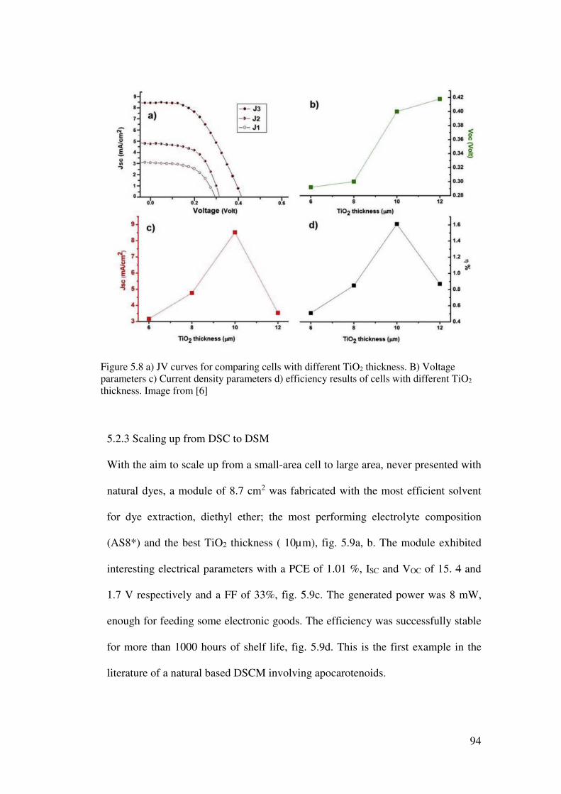
94
5.2.3 Scaling up from DSC to DSM
With the aim to scale up from a small-area cell to large area, never presented with
natural dyes, a module of 8.7 cm2 was fabricated with the most efficient solvent
for dye extraction, diethyl ether; the most performing electrolyte composition
(AS8*) and the best TiO2 thickness ( 10µm), fig. 5.9a, b. The module exhibited
interesting electrical parameters with a PCE of 1.01 %, ISC and VOC of 15. 4 and
1.7 V respectively and a FF of 33%, fig. 5.9c. The generated power was 8 mW,
enough for feeding some electronic goods. The efficiency was successfully stable
for more than 1000 hours of shelf life, fig. 5.9d. This is the first example in the
literature of a natural based DSCM involving apocarotenoids.
Figure 5.8 a) JV curves for comparing cells with different TiO2 thickness. B) Voltage
parameters c) Current density parameters d) efficiency results of cells with different TiO2
thickness. Image from [6]

95
By a simple mathematical procedure (1), I estimate that the natural based-DSSM
produced a battery capacity of 46.8 mA that can be compared to 15 type AAA
alkaline standard batteries of 1200 mAh in the same time (1000).
Battery life= Battery capacity (mAh)/ load current (mA) * 0.7
0.7 is a coefficient that considers the external factor that can influences the battery
life.
Figure 5.9 a) complete DSSM b) dye soaked photoanodes and dye solution c) IV curve of
the best carotenoids-based DSSM d) 1000 hours of shelf-life of the best carotenoids-
based DSSM. Image from [6].

96
5.2.4 Conclusion
I investigated on apocarotenoids extraction with two different solvents in order to
extract an annatto amount with a major content of apolar bixin instead of polar
norbixin. I used an easy protocol for extracting solvents with the aim of lowering
the cost, the time and the use of several solvents. With UV-Vis
spectrophotometric technique, I revealed that diethyl ether is the most sustainable
solvent for extracting an annatto mixture with a high amount of bixin. Indeed,
comparing with the literature, the spectrum obtained with extracted solution by
ethyl ether has the same 3 peaks of pure bixin absorbance spectrum and the
spectrum obtained with solution extracted by acetone is different. I repeat the
absorbance spectra in the solid TiO2 surface with anchored sensitizers and once
again, the solution extracted by diethyl ether demonstrated best results. I
investigated on the electrolyte optimization and the use of TBP additive. Results
show that TBP-free electrolyte is the best choice for a natural based DSSC since
JSC values increase loading to a general boost of the final PCE. I optimized the
TiO2 layer enhancing the thickness from 6 to 10 µm obtaining a gain in JSC (~182
%) and VOC (~33%) resulting in the best PCE of 1.6 % for achiote extract
comparing with literature. For the first time, I present a natural based DSSM with
a PCE of 1% and stable for 1000 hours. I estimated 46.8 Ah of battery capacity
for the shelf life time of the realized natural based module that is the same of more
than 15 standard type AAA alkaline batteries.

97
References
[1] Ritchie R. J., Consistent sets of spectrophotometric chlorophyll equations for
acetone, methanol and ethanol solvents Photosynth. Res., 89, (2006), 27–41.
[2] Calogero G., Citro I., Di Marco G., Armeli Minicante S., Morabito M.,
Genovese G. Brown seaweed pigment as a dye source for photoelectrochemical
solar cells Spectrochim. Acta A, 117, (2014), 702–6.
[3] S.A. Taya, T. M. El-Agez, S. H. El-Ghamri, M. S. Abdel-Latif, Dye-sensitized
solar cells using fresh and dried natural dyes Int. J. Mater. Sci. Appl. 2, (2013),
37–42.
[4] S. Armeli Minicante, E. Ambrosi, M. Back, J. Barichello, E. Cattaruzza, F.
Gonella, E. Scantamburlo, E. Trave. Development of an eco-protocol for seaweed
chlorophylls extraction and possible applications in dye sensitized solar cells. J.
Phys. D: Appl. Phys. 49, (2016), 295601 (7pp).
[5] N. M. Gomez-Ortiz, I. A. Vazquez-Maldonado, A. R. Perez-Espadas, G. J.
Mena-Rejon, J. A. Azamar-Barrios, G. Oskam, Dye-sensitized solar cells with
natural dyes extracted from achiote seeds Sol. Energy. Mater. Sol. Cells, 94,
(2010), 40–4.
[6] G. Calogero, J. Barichello, I. Citro, P. Mariani, L. Vesce, A. Bartolotta, A. Di
Carlo, G. Di Marco. Photoelectrochemical and spectrophotometric studies on dye-
sensitized solar cells (DSCs) and stable modules (DSCMs) based on natural
apocarotenoids pigments. Dyes and Pigments 155, (2018), 75–83.
[7] G Boschloo, L Häggman, A Hagfeldt. Quantification of the effect of 4-tert-
butylpyridine addition to I-/I3 - redox electrolytes in Dye-Sensitized
nanostructured TiO2 Solar Cells. J Phys Chem B, 110, (2006),13144–50.

98
[8] G. Calogero, J. Yum, A. Sinopoli, G. Di Marco, M. Grätzel, MK.
Nazeeruddin, Anthocyanins and betalains as light-harvesting pigments for dye-
sensitized solar cells. Sol Energy, 86, (2012), 1563–75.
[9] S.A. Haque, Y. Tachibana, R.L. Willis, J.E. Moser, M. Grätzel, D.R. Klug,
J.R. Durrant. Parameters influencing charge recombination kinetics in dye-
sensitized nanocrystalline titanium dioxide films. J Phys Chem B, 104, (2000),
538–47.
[10] M. G. Kang, K. S. Ryu, S. H. Chang, N. G. Park, J. S. Hong, K.-J. Kim Bull.
Dependence of TiO2 Film Thickness on Photocurrent-Voltage Characteristics of
Dye-Sensitized Solar Cells. Korean Chem. Soc. 25, (2004), 5.
[11] Dittrich, Porous TiO2: Electron Transport and Application to Dye Sensitized
Injection Solar Cells. T. Phys. Stat. Sol. (a), (2000), 182, 447.
[12] K. Hara; T, Horiguchi; T. Kinoshita; K. Sayama; H. Sugihara; H. Arakawa,
Highly efficient photon-to-electron conversion with mercurochrome-sensitized
nanoporous oxide semiconductor solar cells Sol. Energy Mater. Sol. Cells, (2000),
64, 115.
[13] N.-G. Park, J. Van de Lagemaat, A. Frank, Comparison of Dye-Sensitized
Rutile- and Anatase-Based TiO2 Solar Cells, J. J. Phys. Chem. B, (2000), 104,
8989.
[14] S. Ito, T. Kitamura, Y. Wada, Yanagida, Facile fabrication of mesoporous
TiO2 electrodes for dye solar cells: chemical modification and repetitive coating,
S. Sol. Energy Mater. Sol. Cells (2003), 76, 3.
[15] A. C. Fisher, L. M. Peter, E. A. Ponomarev, A. B. Walker, K. G. U.
Wijayantha, J. Phys. Chem. B, (2000), 104, 949.

99
[16] M. K. Nazeeruddin, R. Humphry-Baker, P. Liska, M. Grätzel, Investigation
of Sensitizer Adsorption and the Influence of Protons on Current and Voltage of a
Dye-Sensitized Nanocrystalline TiO2 Solar Cell J. Phys. Chem. B, (2003), 107,
8981.
[17] M. Grätzel, K. Kalyanasundaram, Artificial photosynthesis: efficient dye-
sensitized photoelectrochemical cells for direct conversion of visible light to
electricity, Curr. Sci. (1994), 66, 706.
[18] S. Ito, K. Ishikawa, C.-J. Wen, S. Yoshida, T. Bull. Watanabe, Dye-
Sensitized Photocells with Meso-Macroporous TiO2 Film Electrodes, Chem. Soc.
Jpn. 2000, 73, 2609.
[19] S. Y. Huang, G. Schlichthörl, A. J. Nozik, M. Grätzel, A .Frank, Charge
Recombination in Dye-Sensitized Nanocrystalline TiO2 Solar Cells, J. J. Phys.
Chem. B, (1997), 101, 2576.
[20] Y. Diamant, S. G. Chen, O. Melamed, A. Zaban, Core−Shell Nanoporous
Electrode for Dye Sensitized Solar Cells: the Effect of the SrTiO3 Shell on the
Electronic Properties of the TiO2 Core, J. Phys. Chem. B, (2003), 107, 1977.
[21] J. Nelson, A. M. Eppler, I. M. Ballard, Photoconductivity and charge
trapping in porous nanocrystalline titanium dioxide, J. Photochem. Photobiol. A.
Chem. (2002), 148, 25.
[22] S. Kambe, S. Nakade, Y. Wada, T. Kitamura, S. Yanagida, Effects of crystal
structure, size, shape and surface structural differences on photo-induced electron
transport in TiO 2 mesoporous electrodes, J. Mater. Chem. 12, (2002), 723.
[23] K.H. Jung, S.R. Jang, R. Vittal, D. Kim, K.J. Kim, Photocurrent
Improvement by Incorporation of Single-wall Carbon Nanotubes in TiO2 Film
Dye-Sensitized Solar Cells. Bulletin of the Korean Chemical Society 24, (2003),
1501-1504.

100
[24] V. Baglio, M. Girolamo, V. Antonucci, S. Arico, Influence of TiO2 film
thickness on the electrochemical behavior of dye-sensitized solar cells. Journal of
Electrochemical Science 6, (2011), 3375-3384.

101
Chapter 6 Carbon based Perovskite Solar Cells- Result and
Discussion
6.1 Characterization and study of the device optimization
The insultaing layer in C-PSC device has the important role of avoiding charge
recombination between the ETM and carbon and of allowing the diffusion of the
perovskite precursor through the mesoporous stack [1]. The small surface area and
the big pore sizes are important features for the spacing layer to favor perovskite
percolation. In the literature, it has already been demonstrated how the
photovoltaic performance are hugely related to the thickness of the ZrO2 [2] but
no works present an optimization of Al2O3 as insultaing layer [3, 4]. I realized C-
PSCs with 1 µm of TiO2 and the chosen thickness is in agreement with studies
already presented in the literature [5]. Al2O3 lays in between and its thickness was
tuned from 0.8 to 1.8 µm; on the top, a carbon layer of 20 µm completes the cell.
The Al2O3 paste is an home made paste developed by an Al2O3 nanoparticles (>50
nm) dispersion in IPA. Six devices were realized for each batch, J0, J1 and J2 that
differ only for the spacing layer thickness. In table 6.1, averaged electrical
parameter are shown. In figure 6.1a, c, and in table 6.1, VOC and FF decrease
when the insulating layer thickness overcome 1.2 µm. VOC values depend on
charge recombination [1] that increase from 1.2 µm to 1.8 µm as it is shown from
dark curves in figure 6.2. This also means an increment of shunt resistance [6] and
the reason of the FF drop down in accordance with the voltage. A thickness
around 0.8-1.2 µm is enough for guaranteeing a good isolation between the ETL
and HTM respectively, ensuring high VOC values around 0.8 V, table 6.1.
On the other hand, a different trend is observed for JSC that reached higher values
in J1 (18.6 mA/cm2) and J2 (16.1 mA/cm2) and lower values in J0 (15.6
mA/cm2). Han et al. [2] reported the same electrical parameters trend with a JSC

102
increment in accordance with the width boost. This behavior connected to an
increment in the Al2O3 width may be attribute to perovskite capacity to harvest
light and transport charge also when growth in Al2O3 [7]. Also in this case, the
current increment from 0.8 to 1.2 Al2O3 µm may be to major a perovskite load in
the mesoporous stack that brings to major light harvester and electron injection.
The slight current decrease from J1 to stack J2 may be to the reduced collection
efficiency. Another effect, already demonstrated in DSSC, is the scattered light
from Al2O3 nanoparticles that reflect the incident photons and this leads to a
current raise [8]. Nevertheless, the optimal thickness is a combination of different
features as the insulating role in avoiding charge recombination and the capacity
to let infiltrate a proper amount of perovskite to increase the light capture. 1.2 µm
results as the best thickness reaching an accordance between different parameters,
table 6.1 and figure 6.1.
Figure 6.1 Dependence of photovoltaic parameters on the Al2O3 thickness for the fabricated
C-PSC: a) Voc, b) Jsc, c) FF and d) PCE. Average and standard deviations are reported for
each batch.
b)
c

103
Tab.6.1 Averaged photovoltaic parameters of each tested batch of C-PSCs. For all
devices, the thickness of the carbon layer was 20 µm. The active area of the cells
is 0.16 cm2.
With the aim at confirming the role that Al2O3 thickness has in avoiding
recombination effects, dark currents were measured for one representative device
of each batch, fig.6.2. The obtained high current in the dark in 1.8 µm, means that
are present recombination effects with a consequent loss in the voltage value as
shown in table 6.1. For insulting thickness of 0.8 and 1.2 µm, current values in the
dark revealed to be lower than 1.8 µm values, in agreement with the higher
voltage, 0.78 and 0.81V respectively.
Fig. 6.2 Dark curves for one representative cell of each batch with 0.8, 1.2 and 1.8
µm of Al2O3.
Batch TiO2
Thickness
[µm]
Al2O3
Thickness
[µm]
Voc [Volt] Jsc [mA/cm2] FF [%] PCE [%]
J0 1 0.8 0.78 ± 0.02 15.57 ± 1.55 67.46 ± 3.09 8.28 ± 0.77
J1 1 1.2 0.81 ± 0.05 18.62 ± 1.59 61.06 ± 7.52 9.135 ±
0.56
J2 1 1.8 0.71 ± 0.05 16.13 ± 1.84 54.97 ± 6.71 6.29 ± 0.75

104
The SEM image shows the entire structure of the best device with a low
magnification, fig. 6.3a, and there is a focus, with high magnification, on the
TiO2/Al2O3 layers where perovskite crystals growth, fig. 6.3b. In SEM images, the
layers thicknesses measured with profilometer are confirmed. Layers boundaries
are well defined and the thickness is uniform showing the goodness of the screen
printer technique. It is possible to observe perovskite crystals of 1 µm, in
accordance with the literature, in the middle of the device. The presence of
crystals in the carbon layer is due to poor carbon porosity and its high thickness
that do not allow the best perovskite infiltration. As discussed before, the carbon
porosity is one issue to overcome in order to improve the performances.
Figure 6.3. SEM images of the J1 device stack: A) low magnification: 7.5 KX of the
entire structure, c-TiO2-mp-TiO2/Al2O3/C b) higher magnification: 20.00 K X to show
TiO2/Al2O3 layers and partially some perovskite crystals. It is shown the device stack that
gave best efficiencies
Al2O3
TiO2
O

105
6.1.2 Characterization and study on the water effect
An interesting water effect was noted when I drop 20 µl of water on the top of the
cell before infiltrating perovskite by a 2-step method. It is observed a PCE
increment in water treated devices and VOC is the main influenced parameter. In
tab. 6.2, electrical parameters report values of treated and no-treated devices. The
water treatment gave a general benefit to device performances with a voltage
increment of 7% respect with the no-treated cell; this is related to a loss in
recombination effects. Best devices reached a PCE of 9.5 % and 11.4 % for no-
treated and treated cell respectively. Both unsealing devices were kept in air
environment in dark and demonstrated a shelf life of more than 30 days without
any significant loss in PCE (fig. 6.4).
Tab. 6.2 – Averaged photovoltaic parameters for each batch of C-PSCs. Batch J1w
represents cells fabricated by using water pre-treatment while J1 without water pre-
treatment. As reported in table 1, TiO2 thickness is 1 µm and Al2O3 thickness is 1.2 µm.
The active area of each cell is 0.16 cm2. Electrical parameters were collected the day of
the cell’s fabrication. MAX PCE refers to the maximum obtained PCE.
After few days, the best efficiency was reached for both devices, 10.9 % and
12.3% for no treated and treated cells respectively, fig. 6.4.
Voltage (V) Jsc
(mA/cm2)
FF (%) PCE (%) MAX PCE
(%)
J1 0.81 ± 0.05 18.62 ± 1.6 61.06 ± 7.5 9.13 ± 0.56 9.52
J1
w
0.87 ± 0.02
(+7%)
19.33 ± 1.7
(+4%)
63.54 ± 2.4
(+4%)
10.66 ± 0.57
(+16%)
11.4

106
Figure 6.5 a) Reverse and forward measures of the best cell in a 0.16 cm2of active area.
The hysteresis effect is not strongly evident b) JV curves of the most efficient cells in the
small area (blue line) and in the large area (red line)
There is no evidence of a strong hysteresis effect as appear in devices made with
SpiroOMeTAD and gold as HTM and counter electrode [9], fig. 6.5a.
Figure 6.6 IPCE of the best cell
Figure 6.4 Shelf-life of the cell without water treatment and with water
a) b)

107
In a larger area device of 1 cm2, produced using the automated printing process
hereby introduced, it resulted in a 7.71% of PCE for 1cm2 of large area, fig. 6.5b.
With the aim to prove the goodness of current measurement, IPCE measurement
was carried out, fig. 6.6, confirming the JSC obtained in JV curves.
In order to evaluate the universality and the veracity of the water effect, I realized
two batches, one of those treated with water, of carbon devices using, this time,
ZrO2 as insulating layer. I observed the same trend: treated batch with water
revealed better PCE performance and the VOC is again the most affected
parameter, fig. 6.7 a, b, c, d.; this experiment was important to demonstrate the
reliability of this effect proving it in other carbon devices with a different spacing
layer.
Figure 6.7 Electrical parameters for carbon devices realized with ZrO2 as insulating layer
However, no differences were observed between ZrO2 and Al2O3 features as
insulating layer, but I prefer to employ Al2O3 layer since, in literature, promising

108
results by using Al2O3 are present in terms of device performances [10].
Several characterizations as Impedance Spectroscopy (IS), X-Ray Diffraction
(XRD) and Light Beam Inducted Currents (LBIC), were carried out in order to
have a better understanding of the water effect and a clear framework of where
and how water acts.
Impedance spectroscopy
IS measurements are useful to study charge transfer processes inside the cell. In
C-PSC, the charge recombination is an effect present at the TiO2/Perovskite
interface, instead the Perovskite/Carbon interface is characterized by charge
transport [11, 12]. IS measurements for treated and no-treated samples were
carried out in the dark, at 0.65 V, fig. 6.9a; the extraction model for C-PSC
devices [11, 12] is shown in figure 6.8. RS, in the extraction model, fig. 6.8,
symbolizes the series resistances between FTO substrate and carbon electrode.
Semicircles at high and low frequencies denote the two interfaces
Perovskite/carbon (RREC) and TiO2/carbon (RCT), respectively. Semicircles of
treated and no treated cells, differ only at low frequencies meaning that the water
treatment influences the perovskite/TiO2 interface while the perovskite/carbon
interface, at high frequencies, is not effected thus for both devices is equal. The
water treatment reduces the charge transfer resistances at low frequencies as
demonstrated from the smaller semicircle of the treated cell in comparison with
that one no treated, fig. 6.9 a. The same effect is also reported at different
voltages, 0.5 and 0.8 V, fig. 6.9 b, c. An example of how water influences the
TiO2 interface is reported also in DSSC technology; in this case, the second
semicircle, thus the TiO2/dye interface, increases because the adsorption of water
blocks dye molecule absorption [13].

109
Figure 6.8 Extraction model for C-PSC device
Figure 6.9 IS measurement for water treated device (blue) and no treated device (red).
Measurement were taken in dark at different bias a) 0.65 V b) 0.5 V and c) 0.8 V
Z (Ω cm2)
a)
b)
c)

110
It is believed that water can promote the nucleation site formation thus influencing
the TiO2/perovskite interface allowing a decrement in charge recombination.
Another possible explanation about the water interaction with TiO2 linked with
the voltage increment, is the water capacity in altering energy level alignment. As
demonstrated several time in literature [14, 15], the environmental pH influences
the TiO2 conduction band as demonstrated in equation 1. In our case, the water
interaction with TiO2 forms –OH groups and the environment becomes slightly
basic. The environmental alkalinity alters the semiconductor conduction band
shifting it to a negative value with a consequent voltage raise as reported in 14
and 15.
ECB (pH) = ECB (pH=0) - 0.059 (pH) (1)
Where ECB (pH=0) for TiO2 anatase is – 0.156 V (vs. NHE) [14, 15].
X-ray diffraction
XRD analysis were performed in order to reveal more information on the amount
and dimension of crystals in treated and no-treated samples, fig. 6.10. I prepare
two samples, compact and m-TiO2/Al2O3/MAPI with and without water addition,
to have a clear framework of how water acts at crystals level; carbon was not
deposit on the surface for allowing peaks detection. The first peak, highlighted in
inset 1, represents the unconverted PbI2, while the second peak, shown in inset 2,
represents the converted PbI2 in perovskite; other peaks refers to FTO/TiO2/Al2O3
as it demonstrated in the literature [10]. Comparing the two PbI2 peaks, between
treated and no treated samples, the ratio for the treated sample, between converted
and unconverted PbI2, is higher (4.5) than that one for untreated sample (3.9), fig.
6.10. This is a clear demonstration of how water helps in PbI2 better conversion in
perovskite. The previous effect is also shown in the literature when, a small

111
amount of water was added to the MAI solution: it seems that water assists the
reaction of PbI2 and MAI promoting a better crystallization of MAPI.
Light Beam Inducted Current
With the aim to have a better assessment on the beneficial effect that water has on
PbI2 conversion in MAPI, as previously demonstrated by XRD, LIBC
measurements were carried out comparing the treated and no-treated samples.
Showing the generated current in a map of 1 cm2 size, LIBC permits to evaluate
the carrier generation process of the perovskite absorber inside the mesoporous
stack. From fig. 6.11, the current map of the water sample is uniform in the whole
device area while, in the no treated sample, the central part has a large
inhomogeneity. In order to better evaluate this effect, in fig. 6.11c, the histogram
of LBIC for each illuminated pixel is plot. In both cases, with and without water
treatment, a normal distribution of the results is obtained but with different
heights and standard deviation. In fact, the water treated cell presents a more
Figure 6.10 XRD analysis of a ample TiO2/Al2O3 after perovskite infiltration with water
treatment (blue line) and w/o water (red line). Figure reveals PbI2 peaks after the perovskite
formation; in the insets, 1) shows the peak of no-converted PbI2 and 2) shows converted
PbI2 peak.

112
pronounced peak and a small standard deviation with respect to the cell without
treatment, which confirm the better homogeneity achieved with water treatment.
This result paves the way for large area and module devices.
Figure 6.11 Light Beam Induced Current (LBIC) maps. a) Current map of the C-PSC
without water treatment b) current map of the C-PSC with water treatment c) Histogram
of current data for the reference cell (green line) and water treated cell (red line)

113
6.1.3 Conclusion
In this research, I optimized the perovskite carbo-based device focusing on
finding the most suitable insulating layer thickness. I developed a home-made
paste of Al2O3, that I used as insulating layer, and found the best thickness at 1.2
µm; this thickness gathers the best accord in terms of current and voltage values.
Indeed, increasing thickness from 1.2 to 1.8 µm, charge recombination effects
occur lowering the voltage values. On the other hand, decreasing the thickness
from 1.2 to 0.8 µm, the load of perovskite is reduced and thus is the light
harvesting that brings to a current decrement. Once finding the best insulating
layer condition with a max PCE of 9.5 %, I studied a water effect with several
characterization measurements in order to evaluate where and how the water
effect acts. Electrical parameters reveal an increment in device performances
loading to enhancement of 16 % of averaged PCE between no treated and water
treated samples. The most influenced parameter is the voltage. IS, XRD and LIBC
measurements detect that the water effects the TiO2/perovskite interface lowering
the charge recombination and so increasing the voltage values. XRD and LIBC
reveal that water can positively influence the perovskite conversion and
distribution in the device mesoporous stack. The effect of water and moisture in
perovskite based devices is still an open topic with controversial opinions; finally,
in this work, I demonstrate a beneficial treatment of water before dropping PbI2,
in a two-step perovskite deposition, that leads to better cell performance and
uniform layers.
6.2 Carbon based module
With the aim at continuing the previous work and scaling up from small area
(0.16 cm2) to large area device, I did a first attempt in building a carbon-based
module. The module was built with the same procedure and same stack

114
parameters (materials, thickness, perovskite solution) applied for small area
devices. The PbI2 solution was deposited by blade coating technique and then
immersed in MAI solution as in small area devices. A module of 17x11.5 cm2,
with 9 cells, of 7.8 mm width for each, an active area (AA) of 101 cm2 and an
aperture area (AR) of 71% (fig. 6.12 a, b) was fabricated with a maximum PCE of
3.6 % in reverse measurement (fig. 6.13).
Figure 6.12 a) Module internal structure b) Realized carbon module
b)
a)

115
The reduced performance respect with correspondent small area device is due to
common issues find in upscaling procedure. The sheet resistance increase when
cells are connected in series or in parallel and when conducting grids on substrates
are deposited leading in a voltage loss and consequently in a low FF value. In the
presented module, no water treatment was used. An LBIC measurement was done
in order to evaluate the current behavior linked with perovskite distribution and its
formation inside the module. As shown in figure 6.14 further improvements must
be done in order to have a complete current distribution so perovskite formation in
the first module cell to allow an increment in current values.
Figure 6.13 IV curve for reverse and forward measurement of the carbon based module

116
Figure 6.14 LBIC measurement in carbon based module. 25% of scanning are in Y axis.
6.3 Characterization and study on carbon planar devices
Here I present for the first time a carbon based planar device. This experiment is a
first attempt in combining the planar with the carbon structure. A planar device
differs from a meso-conventional one for the presence of a SnO2 thin layer of 50
nm that replaces the compact and meso-TiO2, acting as ETL, as explained in
chapter 1 and 4. The advantage of using SnO2 as ETL is avoiding the long
sintering procedures at high temperature that usually TiO2 needs while, 3 hours at
150 °C are sufficient for tin oxide sintering [16]. This reduces the procedure costs
in economical and energetic terms. These devices were realized with a carbon
purchased by Dyenamo that has the great advantage of low and short process for
sintering (120 °C for 10 minutes) and no need of any insulating layer as Al2O3 or
ZrO2. Thanks to the previous feature, it is possible to deposit perovskite before
depositing the carbon avoiding all infiltration problems. Since conventional planar
device showed large enhancement in PCE by the use of triple cation perovskite

117
[17], also in this experiment the triple cation perovskite has been used. This
structure promises benefits in lowering the cost and an easy fabrication procedure.
Eight devices in a carbon-based planar structure were realized and electrical
parameters are shown in tab. 6.3.
Table 6.3 Averaged electrical parameters and the standard deviation for carbon-
planar devices measured under 1.5 AM sun. The active area of measurement is 1
cm2. These data were collected two days after the fabrication and in forward
measurement that demonstrated to be the best scanning for high PCE.
Remarkable results were obtained in terms of PCE with the mean of 9.2 % in 1
cm2. The Fill Factor with a mean value of 55 % remains an issue to overcome.
After four days of shelf life, a device reached the record efficiency of 10.36 %
showing the great potential of this structure. Moreover, some devices were
stressed at 85 °C in the dark and demonstrated incredible high thermal stability.
The best device in terms of stability showed, in figure 6.15, any significant loss in
PCE for more than 400 hours.
VOC (V) JSC (mA/cm2) FF (%) PCE (%)
1.07 ± 0.22 15.55 ± 0.7 55.25 ± 2.8 9.21± 0.4
Figure 6.15 Behavior of normalized PCE for a carbon planar device in 400 hours

118
References
[1] L. Vesce, R. Riccitelli, G. Mincuzzi, A. Orabona, G. Soscia, T. M. Brown, A.
Di Carlo, A. Reale, Fabrication of spacer and catalytic layers in monolithic dye-
sensitized solar cells, IEEE Journal of Photovoltaics 2013, vol. 3 (3), pp. 1004-
1011.
[2] T. Liu, L. Liu, M. Hu, Y. Yang, L. Zhang, A. Mei, H. Han. Critical parameters
in TiO2/ZrO2/Carbon-based mesoscopic perovskite solar cell. Journal of Power
Sources 293, (2015), 533-538.
[3] H. Cheng, S. Yang. Carbon-Based Perovskite Solar Cells without Hole
Transport Materials: The Front Runner to the Market? Adv. Mater. (2017),
1603994.
[4] M. Duan, Y. Hu, A. Mei, Y. Rong, H. Han. Printable carbon-based hole-
conductor-free mesoscopic perovskite solar cells: From lab to market. Materials
Today Energy (2017), 1-11.
[5] A. Mei, X. Li, L. Liu, Z. Ku, T. Liu, Y. Rong, M. Xu, M. Hu, J. Chen, Y.
Yang, M. Grätzel, H. Han. A hole-conductor–free, fully printable mesoscopic
perovskite solar cell with high stability. Science 345, (2014), 295.
[6] A. Hinsch, R. Kinderman, M. Sp¨ath, E. Rijnberg, and J. A. M. von
Roosmalen, “The performance of dye-sensitised solar cells with a one-facial,
monolithic layer built-up prepared by screen printing,” presented at the 2nd World
Conf. Exhibit. Photovoltaic Solar Energy Conversion, Vienna, Austria, 1998.
[7] J. M. Bali, M. M. Lee, A. Hey, H. J. Snaith Low-temperature processed meso-
superstructured to thin-film perovskite solar cells Environ. Sci., 6, (2013), 1739.
[8] Y. Yamamoto, M. Kawaraya, H. Segawa, S. Uchida, J. Kano, F. Saito, K.
Tsujimoto, T. Saito, S. Ito. 10% Efficiency Dye-sensitized Solar Cells Using P25

119
TiO2 Nanocrystalline Electrode Prepared by a Bead-milling Method. Chem. Lett.,
40, (2011),12201222.
[9] H. J. Snaith, A. Abate, J. M. Ball, G. E. Eperon, T. Leijtens, N. K. Noel, S. D.
Stranks, J. Tse-Wei Wang, K. Wojciechowski, W. Zhang. Anomalous Hysteresis
in Perovskite Solar Cells. J. Phys. Chem. Lett. 5, (2014), 1511−1515.
[10] S. Liu, W. Huang, P. Liao, N. Pootrakulchote, H. Li, J. Lu, J. LI, F. Huang,
X. Shai, X. Zhao, Y. Shen, Y. Cheng and M. Wang, J. Mater. Chem. A, 2017.
[11] Z. Meng, D. Guo, J. Yu, K. Fan. Investigation of Al2O3 and ZrO2 spacer
layers for fully printable and hole-conductor-free mesoscopic perovskite solar
cells. Applied Surface Science, 430, (2018), 632–638.
[12] Y. Rong, Z. Ku, A. Mei, T. Liu, M. Xu, S. Ko, X. Li, and H. Han. Hole-
Conductor-Free Mesoscopic TiO2/CH3NH3PbI3 Heterojunction Solar Cells
based on Anatase Nanosheets and Carbon Counter Electrodes. J. Phys. Chem.
Lett, (2014).
[13] S. Mozaffari, M. R. Nateghi, M. Borhanizarandi. Effects of water-based gel
electrolyte on the charge recombination and performance of dye-sensitized solar
cells. J Solid State Electrochem, 18, (2014), 2589–2598.
[14] G. Calogero, J. Yum, A. Sinopoli, G. Di Marco, M. Grätzel, M. K.
Nazeeruddin. Anthocyanins and betalains as light-harvesting pigments for dye-
sensitized solar cells. Solar Energy, 86, (2012), 1563–1575.
[15] K. Kalyanasundaram, M. Grätzel, Applications of functionalized transition
metal complexes in photonic and optoelectronic devices, Coordination Chemistry
Reviews, 177, (1998), 347-414.
[16] E. Calabrò, F. Matteocci, A. L. Palma, L. Vesce, B. Taheri, L. Carlini, I. Pis,
S. Nappini, J. Dagar, C. Battocchio, T. M. Brown, A. Di Carlo, Low temperature,
solution-processed perovskite solar cells and modules with an aperture area

120
efficiency of 11%, Solar Energy Materials and Solar Cells, 185, (2018), 136–144.
[17] E.H. Anaraki, A. Kermanpur, L. Steier, K. Domanski, T. Matsui, W. Tress,
M. Saliba, A. Abate, M. Gratzel, A. Hagfeldt, J.-P. Correa-Baena, Highly efficient
and stable planar perovskite solar cells by solution-processed tin oxide, Energy
Environ. Sci., 9, (2016). 3128–3134.

121
Conclusion
We are living in a world that is facing dramatic and serious environmental
problems; in this framework, despite all research studies in different scientific
fields, I have always been convinced that investing in renewable energies and new
technologies is the most promising strategy to meet our planet emergency. My
PhD research is framed in a multi-fields context varying from biology, crossing
chemistry and physics until electronic engineering. I dedicated these 3 years of
my research to investigate in the photovoltaic field, in two new and promising
technologies of the third-fourth coming generations.
I started my research investigating on the application of Chl-c, which already
shown high potential, in DSSC. With the aim at using a waste product as Undaria
pinantifida, an alien species of brown algae in the venetian lagoon, in the field of
PV technologies, I presented an eco-friendly extraction protocol for obtaining
Chl-c from Undaria in the most economic and simple way. Considering the
molecule polarity, I obtained an eco-friendly and low-cost extraction protocol
mixing a solution with the 60% of acetone and 40% of water. This more polar
solvent, with respect to pure acetone, allows an extraction with a major amount of
Chl-c than Chl-a, as shown from UV-absorbance spectra. The extracted yield was
used as a dye in a DSSC; despite the high efficiency compared with the literature
for the same extraction solvent conditions, the PCE is still low for a real
application in PV technologies. The extraction protocol could find different
application since Chlorophylls are widely used in several fields and much effort
needs for Chlorophyll use in DSSC devices such as the use of disaggregate
additives to ensure an ordered molecules anchorage or additive for preventing the
degradation as ascorbic acid. It is also suggested the use of cocktail dyes mixing
more dyes that absorb at different wavelengths.

122
The same approach thus considering the molecule polarity was used for the
extraction of an annatto mixture with a major amount of bixin, more performant
molecule than norbixin as reported in the literature, both molecules present in
Achiote seeds, a South American fruit. The most sustainable found solvent was
Ethylether; once again the extraction procedure applied was easy, fast and low in
cost, with which, I could obtained the same UV-absorbance spectra of pure bixin
extracted with the long and tedious procedure of chromatography column. Once
optimized the device with a deep investigation on the changing current and
voltage behavior with respect to the thickness and the electrolyte additives, I
obtained the best efficiency present in the literature for carotenoid-based DSSC,
1.6%. At this point, it was a challenge to build a natural based-DSS module. I
built a carotenoid-based DSSM with 1% of PCE without loss in efficiency for
1000 hours. The obtained power is enough for feeding small electronic goods and
this gives to natural-based modules great promises for a real application (in small
scale) since the cost of the dye and the extraction is irrelevant. More works need
to be done in order to increase the efficiency and to keep the same stability under
stressed conditions (light and temperature).
Perovskite Solar Cell is the second PV technology, which I worked with, and I
investigated in my research. I worked on Carbon-based PSC, less efficient but
more stable and much more economic than high-efficiency standard PCE devices.
C-PSC, since the low cost and the already demonstrated stability are more
promising than Spiro and gold based PSC. I found the most suitable thickness for
the use of Al2O3 as insulating layer, describing in details how and why the current
and voltage change with respect the thickness of the spacing layer. Despite all
controversial discussions on the bad water effect on perovskite, studying the C-
PSC device optimization, I found an interesting water effect that positively

123
influenced the perovskite formation, increasing the total PCE of 16%. With
different device characterization such as XRD, LBIC and IS, I found that the
water, in a 2-step deposition, gave beneficial effects on the cell performances. The
most affected parameter is the VOC that increases suggesting a decrease in charge
recombination. The perovskite crystals, in presence of water, showed a better
conversion and a better distribution.
The final step was an evolution to a simple device, even simpler than C-PSC, that
was a planar-carbon device. In a planar-carbon device, made with a new carbon
paste realized by Dyenamo, no high sintering processes are necessary;
mesoporous TiO2 and Al2O3 are replaced by a thin layer of SnO2 and these reduce
the energetic consumption and materials and fabrication costs. Remarkable results
in terms of efficiency with a max PCE of 10.4% in 1cm2 was reached and thermal
stability for 400 °C. The planar-carbon device has been a really first attempt but it
promises great potential for growing the PCE and stability.

124
Publications
• Journal articles
1) ‘Development of an eco-protocol for seaweed chlorophylls extraction and
possible applications in dye sensitized solar cells.’ Simona Armeli
Minicante, Emanuele Ambrosi, Michele Back, Jessica Barichello, Elti
Cattaruzza, Francesco Gonella, Enrico Scantamburlo, Enrico Trave.
Journal of Physics D: Applied Physics 49 (2016)
2) ‘Photoelectrochemical and spectrophotometric studies on dye-sensitized
solar cells (DSCs) and stable modules (DSCMs) based on natural
apocarotenoids pigments’; Giuseppe Calogero, Jessica Barichello, Ilaria
Citro, Paolo Mariani, Luigi Vesce, Antonino Bartolotta, Aldo Di Carlo
and Gaetano Di Marco
Dyes and Pigments 155 (2018) 75–83
DOI: 10.1016/j.dyepig.2018.03.021
3) Jessica Barichello. ‘Elettricità rinnovabile dal Sole’ in OFFICINA*,
n.18, agosto-settembre 2017, ISSN, 2532-1218

125
• Oral contributions
1) Italian Photochemistry Meeting 2017, December 2017, Perugia
Photoelectrochemical study on photovoltaics devices based on natural
carotenoids pigments.
Jessica Barichello, Giuseppe Calogero, Ilaria Citro, Paolo Mariani, Luigi
Vesce, Antonino Bartolotta, Aldo Di Carlo and Gaetano Di Marco
2) International Conference on Terahertz emission, Metamaterials and
Nanophotonics,TERAMETANANO-June 2017, Venice, Italy
‘Carbon-based Perovskite Solar Cells’
Invited speaker. Jessica Barichello, Fabio Matteocci, Enrico
Lamanna, Alessandro Palma, Aldo di Carlo
• Poster contributions
1) 3rd International Conference on Perovskite Solar Cells and
Optoelettronics. 18-20 Settembre 2017, Oxford, UK
Jessica Barichello, F. Matteocci, E. Lamanna, S. Yadav, A. Di Carlo-
‘Carbon-based Perovskite Solar Cells with A2O3 insulating layer’
2) Materials 2016, 12-16 December 2016, Aci Castello (Catania)
‘High-efficiency Dye-Sensitized Solar Cell co-sensitized with Gold
Nanoparticles Embedded in mesoscopic TiO2’ J. Barichello, M.
Mardegan, E. Scantamburlo , G. Calogero, G. Di Marco, S. Polizzi
3) Materials 2016, 12-16 December 2016, Aci Castello (Catania)
‘Ruthenium-based dye-sensitized solar cells: future and perspective’

126
Giuseppe Calogero, Jessica Barichello, Antonino Bartolotta and Gaetano
Di Marco.
4) International Conference on Perovskite Solar Cells and Opotoelectronics-
26-29 September 2016, Genova, Italy
Andreas Hisch, Simone Mastroianni, Lukas Wagner, Jessica Barichello,
Gayatri Mathiazhagan-‘ Developments for stable lowest-cost-in-situ
perovskite solar modules’
5) International Conference on Hybrid and Organic Photovoltaics
(HOPV16)- 29th June- 1 st July 2016 Swansea, UK
Jessica Barichello, Antonio Bartolotta, Giuseppe Calogero, Gaetano di
Marco_ Extraction and characterization of apocarotenoids (cis-norbixin
and cis-bixin) as natural sensitizers for dyesensitized solar cells
6) International Conference on Hybrid and Organic Photovoltaics
(HOPV16)- 29th June- 1 st July 2016 Swansea, UK
Jessica Barichello, Simona Armeli Minicante, Giuseppe Calogero, G. Di
Marco, Francesco Gonella, Enrico Trave- ‘Chlorophyll-c from marine
algae and its characterization as natural dye for dye-sensitized solar cells’
7) International Conference on Hybrid and Organic Photovoltaics (HOPV16)
Swansea, United Kingdom, 2016 June 29th - July 1st
Jessica Barichello, Antonio Bartolotta, Giuseppe Calogero
‘Extraction and Characterization of Black Carrots as Natural Sensitizers
for Dye-Sensitized Solar Cells’
8) International Conference on Hybrid and Organic Photovoltaics (HOPV16)
Swansea, United Kingdom, 2016 June 29th - July 1st
‘Hybrid-organic sensitizers for highly efficient dye-sensitized solar cells’

127
Giuseppe Calogero, Jessica Barichello, Antonino Bartolotta and Gaetano
Di Marco.
PhD Schools and curses
1) Attending PhD School “Isophos 2018” (International School on Hybrid
and Organic Photovoltaics, Castiglione della Pescaia 2- 6 September 2018)
2) Attending PhD School ‘School on Molecular and Biophysical Aspects of
Photosynthesis’
(January 25-29, 2016, Venice)
3) Curses on Geographical Information Systems (GIS), Environmental Data
Analysis, Science of Complex Systems and Scientific writing successfully
passed
Project
‘ESPResSO’ supported by the European Union’s Horizon 2020 Framework
Program for funding Research and Innovation under Grant agreement no.
764047

128
Many Thanks…
For the realization of my PhD work and thesis, my most sincerely
thanks goes to Professor Francesco Gonella, Dr. Giuseppe Calogero
(CNR researcher) and Professor Aldo di Carlo.
I thank Professor Francesco Gonella, for fundamental advices during
my PhD and for having deeply reviewed my thesis.
I thank Professor Giuseppe Calogero for having assisted my research
with fruitful suggestion, inspiring and cheering me during hard
working periods. G. C. taught me patiently the lab activities hosting
me at CNR-IPCF in Messina and giving me precious ideas and
important knowledge in the DSSC field. Moreover, G.C. helped me
steadily during the writing of my PhD thesis, being always present
also at distance.
I thank Professor Aldo di Carlo, for the great opportunity to work in
his team, in laboratory CHOSE at University of TorVergata of Rome,
a brilliant and stimulating environment. Here, I worked on the PSC
field, collaborating with great and expert collegues.
I thank Professor Andreas Hinsh for having host me 6 months in his
laboratories at Fraunhofer ISE, in Freiburg in Germany and having
teach me how to work with Carbon-based Perovskite Solar Cells.
I really thank Professor Stefano Polizzi for gave me the chance to
move to Messina for learning significant information in DSSC field,

129
contributing to my research and to my formation.
I thank all my colleagues in CHOSE, Fabio Matteocci, Luigi Vesce,
Paolo Mariani, Valentina Mirruzzo, Luigi Angelo Castriotta,
Alessandro Lanuti, Emanuele Calabrò, Enrico Lamanna and in
Fraunhofer ISE, Simone Mastroianni for the work and the laughs in
and outside the lab.
I thank Simona Armeli Minicante for having convinced me to start my
PhD and for the positive answers to many of my doubts during
stressing working time.
More important, I thank my family, my mother and father, without
them, nothing would have been possible.
And I thank Maurizio for having always been with me.