Embed Size (px)
Citation preview

Si5348-D Evaluation Board Users Guide
The Si5348-D-EVB is used for evaluating the Si5348 NetworkSynchronizer Clock for SyncE1588 and Stratum 33E applica-tions The device revision is distinguished by a white 1 inch x0187 inch label with the text ldquoSI5348-D-EBrdquo in the lower left-hand corner of the board (For ordering purposes only the termsldquoEBrdquo and ldquoEVBrdquo refer to the board and the kit respectively In thisdocument the terms are synonymous in context) The Si5348contains three independent DSPLLs in a single IC with program-mable jitter attenuation bandwidth on a per DSPLL basis TheSi5348-D-EVB supports three independent differential inputclocks two independent CMOS input clocks and seven inde-pendent output clocks via onboard SMA connectors The Si5348-D-EVB can be controlled and configured via a USB connection toa host PC running Silicon Labsrsquo next generation Clock BuilderProtrade (CBProtrade) software tool Test points are provided on-boardfor external monitoring of supply voltagesThe device revision is distinguished by a white 1 inch x 0187 inch label with the textldquoSI5348-D-EBrdquo installed in the lower left hand corner of the board (For ordering purpo-ses only the terms ldquoEBrdquo and ldquoEVBrdquo refer to the board and the kit respectively For thepurpose of this document the terms are synonymous in context
EVB FEATURES
bull Powered from USB port or external +5 Vpower supply via screw terminals
bull Included SiOCXO1-EB reference OCXOboard allows for evaluation in standaloneand holdover mode
bull CBProtrade GUI programmable VDD supplyallows device supply voltages from 3325 or 18 V
bull CBProtrade GUI programmable VDDOsupplies allow each of the seven outputs tohave its own supply voltage selectablefrom 33 25 or 18 V
bull CBProtrade GUI allows control andmeasurement of voltage current andpower of VDD and all 8 VDDO supplies
bull Status LEDs for power supplies andcontrolstatus signals of Si5348
bull SMA connectors for input clocks outputclocks and optional external timingreference clock
silabscom | Smart Connected Energy-friendly Rev 09
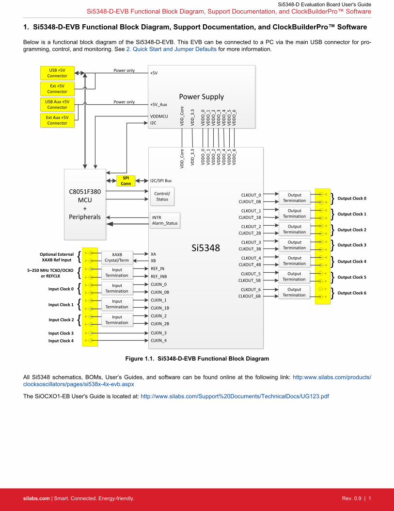
1 Si5348-D-EVB Functional Block Diagram Support Documentation and ClockBuilderProtrade Software
Below is a functional block diagram of the Si5348-D-EVB This EVB can be connected to a PC via the main USB connector for pro-gramming control and monitoring See 2 Quick Start and Jumper Defaults for more information
Si5348
CLKOUT_0CLKOUT_0B
OutputTermination
CLKOUT_1CLKOUT_1B
OutputTermination
CLKOUT_2CLKOUT_2B
OutputTermination
CLKOUT_3CLKOUT_3B
OutputTermination
CLKOUT_4CLKOUT_4B
OutputTermination
CLKOUT_5CLKOUT_5B
OutputTermination
InputTermination
InputTermination
InputTermination
XAXB
REF_IN
REF_INB
CLKIN_0
CLKIN_0B
CLKIN_1
CLKIN_1B
Power Supply
C8051F380MCU
+Peripherals
I2CSPI Bus
VDDO
_0
VDD_
Core
VDD_
33
VDDO
_1VD
DO_2
VDDO
_3VD
DO_4
VDDO
_5
VDDO
_0
VDD_
Core
VDD_
33
VDDO
_1VD
DO_2
VDDO
_3VD
DO_4
VDDO
_5
USB +5V Connector
USB Aux +5VConnector
Ext +5VConnector
I2C
+5V
+5V_Aux
VDDMCU
5ndash250 MHz TCXOOCXO or REFCLK
Input Clock 0 Input Clock 1
Output Clock 0
Output Clock 1
Output Clock 2
Output Clock 3
Output Clock 4
Output Clock 5
Power only
Power only
ControlStatus
INTRAlarm_Status
InputTermination
CLKIN_2
CLKIN_2B
VDDO
_6VD
DO_6
CLKOUT_6CLKOUT_6B
OutputTermination Output Clock 6
Ext Aux +5VConnector
SPI Conn
Optional ExternalXAXB Ref Input XAXB
CrystalTerm
Input Clock 3
Input Clock 4
CLKIN_3
CLKIN_4
Input Clock 2
Figure 11 Si5348-D-EVB Functional Block Diagram
All Si5348 schematics BOMs Userrsquos Guides and software can be found online at the following link httpwwwsilabscomproductsclocksoscillatorspagessi538x-4x-evbaspx
The SiOCXO1-EB Users Guide is located at httpwwwsilabscomSupport20DocumentsTechnicalDocsUG123pdf
Si5348-D Evaluation Board Users GuideSi5348-D-EVB Functional Block Diagram Support Documentation and ClockBuilderProtrade Software
silabscom | Smart Connected Energy-friendly Rev 09 | 1
2 Quick Start and Jumper Defaults
1 Install ClockBuilderPro desktop software from EVB support web page given in Section 22 Connect USB cable from Si5348-D-EVB to PC with ClockBuilderPro software installed3 Connect the SIOCXO1-EB to the reference input using the included SMA cable4 Leave the jumpers as installed from the factory and launch the ClockBuilderPro software5 You can use ClockBuilderPro to create download and run a frequency plan on the Si5348-D-EVB6 For the Si5348 data sheet go to httpwwwsilabscomtiming
Table 21 Si5348-D EVB Jumper Defaults
Location Type I = Installed O =Open
Location Type I = Installed O =Open
JP1 2 pin I JP23 2 pin O
JP2 2 pin I JP24 2 pin O
JP3 2 pin I JP25 2 pin O
JP4 2 pin I JP26 2 pin O
JP5 2 pin O JP27 2 pin O
JP6 2 pin O JP28 2 pin O
JP7 2 pin I JP29 2 pin O
JP8 2 pin O JP30 2 pin O
JP9 2 pin O JP31 2 pin O
JP10 2 pin I JP32 2 pin O
JP13 2 pin O JP33 2 pin O
JP14 2 pin I JP34 2 pin O
JP15 3 pin 1 to 2 JP35 2 pin O
JP16 3 pin 1 to 2 JP36 2 pin O
JP17 2 pin O JP38 3 pin All open
JP18 2 pin O JP39 2 pin O
JP19 2 pin O JP40 2 pin O
JP20 2 pin O JP41 2 pin O
JP21 2 pin O
JP22 2 pin O J36 5x2 Hdr All 5 installed
Note Refer to the Si5348-D-EVB schematics for the functionality associated with each jumper
Si5348-D Evaluation Board Users GuideQuick Start and Jumper Defaults
silabscom | Smart Connected Energy-friendly Rev 09 | 2
3 Status LEDs
Table 31 Si5348-D EVB Status LEDs
Location Silkscreen Color Status Function Indication
D27 5VUSBMAIN Blue Main USB +5 V present
D22 3P3V Blue DUT +33 V is present
D26 VDD DUT Blue DUT VDD Core voltage present
D25 INTR Red MCU INTR (Interrupt) active
D21 READY Green MCU Ready
D24 BUSY Green MCU Busy
D5 LOL_T0B Blue Loss of Lock - DSPLL C
D6 LOL_T4B Blue Loss of Lock - DSPLL D
D8 LOS2B Blue Loss of Signal at IN2
D11 INTRB Blue Si5348 Interrupt Active
D12 LOS1B Blue Loss of Signal at IN1
D13 LOL_AB Blue Loss of Lock DSPLL A
D14 LOS0B Blue Loss of Signal at IN0
D27 D22 and D26 are illuminated when USB +5 V Si5348-D-EVB +33 V and Si5348 VDD or supply voltages respectively arepresent D25 D21 and D24 are status LEDs showing on-board MCU activity LEDs D14 D12 and D8 indicate loss of signal at clockinputs IN0 IN1 and IN2 respectively LEDs D13 D5 and D6 indicate loss of lock for one of three internal DSPLLs (A C and D) re-spectively D11 indicates Si5348 interrupt output is active (as configured by Si5348 register programming) LED locations are highligh-ted below with LED function name indicated on board silkscreen
Figure 31 Si5348-D-EVB LED Locations
Si5348-D Evaluation Board Users GuideStatus LEDs
silabscom | Smart Connected Energy-friendly Rev 09 | 3
4 External Reference Input (XAXB)
An external timing reference (48 MHz XTAL) is used in combination with the internal oscillator to produce an ultra-low jitter referenceclock for the DSPLL and for providing a stable reference for the free-run and holdover modes The Si5348-D-EVB can also accommo-date an external reference clock instead of a crystal To evaluate the device with an external REFCLK C111 and C113 must be popula-ted and XTAL Y1 removed (see figure below) The REFCLK can then be applied to SMA connectors J39 and J40
Figure 41 External Reference Input Circuit
Si5348-D Evaluation Board Users GuideExternal Reference Input (XAXB)
silabscom | Smart Connected Energy-friendly Rev 09 | 4
5 Clock Input and Output Circuits
51 Clock Input Circuits (REFREFB IN0IN0B-IN2IN2B IN3 IN4)
The Si5348-D-EVB has eight SMA connectors (REFREFB IN0IN0BndashIN2IN2B) for receiving external differential clock signals TheREFREFB differential input clock is intended to support a TCXO or OCXO such as the included SiOCXO1-EB which determines theSi5348rsquos wander performance (Please note that this input clock is different from the optional reference clock that may be applied at XAXB) All differential input clocks are terminated as shown in the figure below The only exception is that the terminating 499 Ω resistorfor REF is not installed This is R84 corresponding to IN0s R76 in the figure below The reason for this exception is that single-endedTCXOs and OCXOs typically cannot drive a 50 Ω load Note that input clocks are ac-coupled and 50 Ω terminated This represents fourdifferential input clock pairs Single-ended clocks can be used by appropriately driving one side of the differential pair with a single-ended clock For details on how to configure inputs as single-ended please refer to the Si5348 data sheet
Figure 51 Differential Input Clock Termination Circuit
In addition the Si5348-D-EVB supports two SMA connectors (IN3 IN4) for receiving external single-ended LVCMOS clocks Each ofthese clocks connects to its respective Si5348 pins via a single installed 0 Ω resistor There are no other termination components onthe EVB
Si5348-D Evaluation Board Users GuideClock Input and Output Circuits
silabscom | Smart Connected Energy-friendly Rev 09 | 5
52 Clock Output Circuits (OUTxOUTxB)
Each of the 14 output drivers (seven differential pairs OUT0OUT0BmdashOUT6OUT6B) is ac-coupled to its respective SMA connectorThe output clock termination circuit is shown in the figure below The output signal will have no dc bias If dc coupling is required the accoupling capacitors can be replaced with a resistor of appropriate value In particular if differential pair OUT6OUT6B is configured for 1Hz output then the AC coupling output capacitors C166 and C168 each need to be replaced by a 0 Ω resistor (These capacitors arethe respective counterparts of the OUT0OUT0B output capacitors C25 and C27 in the figure below) The Si5348-D-EVB providespads for optional output termination resistors andor low-frequency capacitors Note that components with schematic ldquoNIrdquo designationare not normally populated on the Si5348-D-EVB and provide locations on the PCB for optional dcac terminations by the end user
Figure 52 Output Clock Termination Circuit
Si5348-D Evaluation Board Users GuideClock Input and Output Circuits
silabscom | Smart Connected Energy-friendly Rev 09 | 6
6 Using the Si5348-D-EVB and Installing ClockBuilderPro (CBPro) Desktop Software
61 Installing ClockBuilderPro (CBPro) Desktop Software
To install the CBPro software on any Windows 7 (or above) PC
Go to httpwwwsilabscomCBPro and download ClockBuilderPro software
Installation instructions and Userrsquos Guide for ClockBuilder can be found at the download link shown above Please follow the instruc-tions as indicated
62 Connecting the EVB to Your Host PC
Once ClockBuilderPro software is installed connect to the EVB with a USB cable as shown below
Figure 61 EVB Connection Diagram
Si5348-D Evaluation Board Users GuideUsing the Si5348-D-EVB and Installing ClockBuilderPro (CBPro) Desktop Software
silabscom | Smart Connected Energy-friendly Rev 09 | 7
63 Additional Power Supplies
The Si5348-EB comes pre-configured with jumpers installed at JP15 and JP16 (pins 1ndash2 in both cases) in order to select ldquoUSBrdquo Thesejumpers together with the components installed configure the evaluation board to obtain all +5 V power solely through the main USBconnector at J37 This setup is the default configuration and should normally be sufficient
The general guidelines for single USB power supply operation are listed belowbull Use either a USB 30 or USB 20 port These ports are specified to supply 900 mA and 500 mA respectively at +5 Vbull If you are working with a USB 20 port and you are current limited turn off enough DUT output voltage regulators to drop the total
DUT current le 470 mA (Note USB 20 ports may supply gt 500 mA Provided the nominal +5 V drops gracefully by less than 10the EVB will still work)
bull If you are working with a USB 20 and you are current limited and need all output clock drivers enabled re-configure the EVB todrive the DUT output voltage regulators from an external +5 V power supply as followsbull Connect external +5 V power supply to terminal block J33 on the back side of the PCBbull Move the jumper at JP15 from pins 1ndash2 USB to pins 2ndash3 EXT
Errata Note The Si5348-EB REV 10 silkscreen at jumpers JP15-16 is reversed ie the ldquoUSBrdquo and ldquoEXTrdquo text are incorrectly swappedNormal operation from USB only is still with jumpers installed between pins 1ndash2 This is on the right-hand side as viewed reading thesilkscreen choices
Si5348-D Evaluation Board Users GuideUsing the Si5348-D-EVB and Installing ClockBuilderPro (CBPro) Desktop Software
silabscom | Smart Connected Energy-friendly Rev 09 | 8
64 Overview of ClockBuilderPro Applications
Note The following instructions and screen captures may vary slightly depending on your version of ClockBuilder Pro
The ClockBuilderPro installer will install two main applications
Figure 62 Application 1 ClockbuilderPro Wizard
Use the CBPro Wizard tobull Create a new designbull Review or edit an existing designbull Export create in-system programming files
Si5348-D Evaluation Board Users GuideUsing the Si5348-D-EVB and Installing ClockBuilderPro (CBPro) Desktop Software
silabscom | Smart Connected Energy-friendly Rev 09 | 9
Figure 63 Application 2 EVB GUI
Use the EVB GUI tobull Download configuration to EVBrsquos DUT (Si5348)bull Control the EVBrsquos regulatorsbull Monitor voltage current and power on the EVB
65 Common ClockBuilderProWork Flow Scenarios
There are three common workflow scenarios when using CBPro and the Si5348-D EVB These workflow scenarios arebull Workflow Scenario 1 Testing a Silicon Labs-Created Default Configurationbull Workflow Scenario 2 Modifying the Default Silicon Labs-Created Device Configurationbull Workflow Scenario 3 Testing a User-Created Device Configuration
Each is described in more detail in the following sections
Si5348-D Evaluation Board Users GuideUsing the Si5348-D-EVB and Installing ClockBuilderPro (CBPro) Desktop Software
silabscom | Smart Connected Energy-friendly Rev 09 | 10
66 Workflow Scenario 1 Testing a Silicon Labs-Created Default Configuration
The flow for using the EVB GUI to initialize and control a device on the EVB is as follows
Once the PC and EVB are connected launch ClockBuilder Pro by clicking on this icon on your PCrsquos desktop
Figure 64 ClockBuilderPro Desktop Icon
If an EVB is detected click on the ldquoOpen Default Planrdquo button on the Wizardrsquos main menu CBPro automatically detects the EVB anddevice type
Figure 65 Open Default Plan
Once you open the default plan (based on your EVB model number) a popup will appear
Si5348-D Evaluation Board Users GuideUsing the Si5348-D-EVB and Installing ClockBuilderPro (CBPro) Desktop Software
silabscom | Smart Connected Energy-friendly Rev 09 | 11
Figure 66 Write Design to EVB Dialog
Select ldquoYesrdquo to write the default plan to the Si5348 device mounted on your EVB This ensures the device is completely reconfiguredper the Silicon Labs default plan for the DUT type mounted on the EVB
Figure 67 Writing Design Status
After CBPro writes the default plan to the EVB click on ldquoOpen EVB GUIrdquo as shown below
Figure 68 Open EVB GUI
The EVB GUI will appear Note all power supplies will be set to the nominal values defined in the devicersquos default CBPro project filecreated by Silicon Labs as shown in the example session window below
Si5348-D Evaluation Board Users GuideUsing the Si5348-D-EVB and Installing ClockBuilderPro (CBPro) Desktop Software
silabscom | Smart Connected Energy-friendly Rev 09 | 12
Figure 69 EVB GUI Window
Si5348-D Evaluation Board Users GuideUsing the Si5348-D-EVB and Installing ClockBuilderPro (CBPro) Desktop Software
silabscom | Smart Connected Energy-friendly Rev 09 | 13
661 Verify Free-Run Mode Operation
Assuming no external clocks have been connected to the INPUT CLOCK differential SMA connectors (labeled ldquoINxINxBrdquo) locatedaround the perimeter of the EVB the DUT should now be operating in free-run mode as the DUT will be locked to the crystal in thiscase
You can run a quick check to determine if the device is powered up and generating output clocks (and consuming power) by clicking onthe Read All button highlighted above and then reviewing the voltage current and power readings for each VDDx supply
Note Shutting ldquoOffrdquo then ldquoOnrdquo of the VDD and VDDA supplies will power-down and reset the DUT Every time you do this to reload theSilicon Labs-created default plan into the DUTrsquos register space you must go back to the Wizardrsquos main menu and select ldquoWrite Designto EVBrdquo
Figure 610 Write Design to EVB
Failure to do the step above will cause the device to read in a preprogrammed plan from its non-volatile memory (NVM) How-ever the plan loaded from the NVM may not be the latest plan recommended by Silicon Labs for evaluation
At this point you should verify the presence and frequencies of the output clocks (running to free-run mode from the crystal) using ap-propriate external instrumentation connected to the output clock SMA connectors To verify the output clocks are toggling at the correctfrequency and signal format click on View Design Report as highlighted below
Si5348-D Evaluation Board Users GuideUsing the Si5348-D-EVB and Installing ClockBuilderPro (CBPro) Desktop Software
silabscom | Smart Connected Energy-friendly Rev 09 | 14
Figure 611 View Design Report
Your configurationrsquos design report will appear in a new window as shown below Compare the observed output clocks to the frequen-cies and formats noted in your default projectrsquos Design Report
Si5348-D Evaluation Board Users GuideUsing the Si5348-D-EVB and Installing ClockBuilderPro (CBPro) Desktop Software
silabscom | Smart Connected Energy-friendly Rev 09 | 15
Figure 612 Design Report Window
662 Verify Locked Mode Operation
Assuming you connect the correct input clocks to the EVB (as noted in the Design Report shown above) the DUT on your EVB will berunning in ldquolockedrdquo mode
Si5348-D Evaluation Board Users GuideUsing the Si5348-D-EVB and Installing ClockBuilderPro (CBPro) Desktop Software
silabscom | Smart Connected Energy-friendly Rev 09 | 16
67 Workflow Scenario 2 Modifying the Default Silicon Labs-Created Device Configuration
To modify the ldquodefaultrdquo configuration using the CBPro Wizard click on any of the underlined fields below the header Edit Configurationwith Wizard You can also pull down on the Design Dashboard menu and select a design step
Figure 613 Edit Configuration with Wizard
You will now be taken to the Wizardrsquos step-by-step menus to allow you to change any of the default planrsquos operating configurations
Si5348-D Evaluation Board Users GuideUsing the Si5348-D-EVB and Installing ClockBuilderPro (CBPro) Desktop Software
silabscom | Smart Connected Energy-friendly Rev 09 | 17
Figure 614 Design ID and Notes
Note you can click on the icon on the lower left hand corner of the menu to confirm if your frequency plan is valid After making yourdesired changes you can click on Write to EVB to update the DUT to reconfigure your device in real time The Design Write statuswindow will appear each time you make a change
Figure 615 Writing Design Status
Si5348-D Evaluation Board Users GuideUsing the Si5348-D-EVB and Installing ClockBuilderPro (CBPro) Desktop Software
silabscom | Smart Connected Energy-friendly Rev 09 | 18
68 Workflow Scenario 3 Testing a User-Created Device Configuration
To test a previously created user configuration open the CBPro Wizard by clicking on the icon on your desktop and then selectingOpen Design Project File
Figure 616 Open Design Project File
Locate your CBPro design file (slabtimeproj or sitproj file) in the Windows file browser
Si5348-D Evaluation Board Users GuideUsing the Si5348-D-EVB and Installing ClockBuilderPro (CBPro) Desktop Software
silabscom | Smart Connected Energy-friendly Rev 09 | 19
Figure 617 Browse to Project File
Select Yes when the WRITE DESIGN to EVB popup appears
Figure 618 Write Design to EVB Dialog
The progress bar will be launched Once the new design project file has been written to the device verify the presence and frequenciesof your output clocks and other operating configurations using external instrumentation
Si5348-D Evaluation Board Users GuideUsing the Si5348-D-EVB and Installing ClockBuilderPro (CBPro) Desktop Software
silabscom | Smart Connected Energy-friendly Rev 09 | 20
69 Exporting the Register Map File for Device Programming by a Host Processor
You can also export your configuration to a file format suitable for in-system programming by selecting Export as shown below
Figure 619 Export Register Map File
You can now write your devicersquos complete configuration to file formats suitable for in-system programming
Si5348-D Evaluation Board Users GuideUsing the Si5348-D-EVB and Installing ClockBuilderPro (CBPro) Desktop Software
silabscom | Smart Connected Energy-friendly Rev 09 | 21
Figure 620 Export Settings
Si5348-D Evaluation Board Users GuideUsing the Si5348-D-EVB and Installing ClockBuilderPro (CBPro) Desktop Software
silabscom | Smart Connected Energy-friendly Rev 09 | 22
7 Writing a New Frequency Plan or Device Configuration to Non-Volatile Memory (OTP)
Note Writing to the device non-volatile memory (OTP is NOT the same as writing a configuration into the Si5348 using ClockBuilder-PRo on the Si5348-D EVB) Writing a configuration into the EVB from ClockBuilderPro is done using Si5348 RAM space and can bedone a virtually unlimited numbers of times Writing to OTP is limited as described below
Refer to the Si534x8x Family Reference Manuals and device data sheets for information on how to write a configuration to the EVBDUTrsquos non-volatile memory (OTP) The OTP can be programmed a maximum of two times only Care must be taken to ensure thedesired configuration is valid when choosing to write to OTP
Si5348-D Evaluation Board Users GuideWriting a New Frequency Plan or Device Configuration to Non-Volatile Memory (OTP)
silabscom | Smart Connected Energy-friendly Rev 09 | 23
8 Serial Device Communications (Si53848 lt-gt MCU)
81 On-Board SPI Support
The MCU onboard the Si5348-D-EVB communicates with the Si5348 device through a 4-wire SPI (Serial Peripheral Interface) link TheMCU is the SPI master and the Si5348 device is the SPI slave The Si5348 device can also support a 2-wire I2C serial interface al-though the Si5348-D-EVB does NOT support the I2C mode of operation SPI mode was chosen for the EVB because of the relativelyhigher speed transfers supported by SPI vs I2C
82 External I2C Support
I2C can be supported if driven from an external I2C controller The serial interface signals between the MCU and Si5348 pass throughshunts loaded on header J36 These jumper shunts must be installed in J36 for normal EVB operation using SPI with CBPro If testingof I2C operation via external controller is desired the shunts in J36 can be removed thereby isolating the on-board MCU from theSi5348 device The shunt at J4 (I2C_SEL) must also be removed to select I2C as Si5348 interface type An external I2C controller con-nected to the Si5348 side of J36 can then communicate to the Si5348 device (For more information on I2C signal protocol please referto the Si5348 data sheet)
The figure below illustrates the J36 header schematic J36 even numbered pins (2 4 6 etc) connect to the Si5348 device and the oddnumbered pins (1 3 5 etc) connect to the MCU Once the jumper shunts have been removed from J36 and J4 I2C operation shoulduse J36 pin 4 (DUT_SDA_SDIO) as the I2C SDA and J36 pin 8 (DUT_SCLK) as the I2C SCLK Please note the external I2C controllerwill need to supply its own I2C signal pull-up resistors
Figure 81 Serial Communications Header J36
Si5348-D Evaluation Board Users GuideSerial Device Communications (Si53848 lt-gt MCU)
silabscom | Smart Connected Energy-friendly Rev 09 | 24
9 Si5348-D-EVB Schematic and Bill of Materials (BOM)
The Si5348-D-EVB Schematic and Bill of Materials (BOM) can be found online at
httpwwwsilabscomproductsclocksoscillatorspagessi538x-4x-evbaspx
Note Please be aware that the Si5348-D-EVB schematic is in OrCad Capture hierarchical format and not in a typical ldquoflatrdquo schematicformat
Si5348-D Evaluation Board Users GuideSi5348-D-EVB Schematic and Bill of Materials (BOM)
silabscom | Smart Connected Energy-friendly Rev 09 | 25
httpwwwsilabscom
Silicon Laboratories Inc400 West Cesar ChavezAustin TX 78701USA
ClockBuilder ProOne-click access to Timing tools documentation software source code libraries amp more Available for Windows and iOS (CBGo only)
wwwsilabscomCBPro
Timing Portfoliowwwsilabscomtiming
SWHWwwwsilabscomCBPro
Qualitywwwsilabscomquality
Support and Communitycommunitysilabscom
DisclaimerSilicon Laboratories intends to provide customers with the latest accurate and in-depth documentation of all peripherals and modules available for system and software implementers using or intending to use the Silicon Laboratories products Characterization data available modules and peripherals memory sizes and memory addresses refer to each specific device and Typical parameters provided can and do vary in different applications Application examples described herein are for illustrative purposes only Silicon Laboratories reserves the right to make changes without further notice and limitation to product information specifications and descriptions herein and does not give warranties as to the accuracy or completeness of the included information Silicon Laboratories shall have no liability for the consequences of use of the information supplied herein This document does not imply or express copyright licenses granted hereunder to design or fabricate any integrated circuits The products are not designed or authorized to be used within any Life Support System without the specific written consent of Silicon Laboratories A Life Support System is any product or system intended to support or sustain life andor health which if it fails can be reasonably expected to result in significant personal injury or death Silicon Laboratories products are not designed or authorized for military applications Silicon Laboratories products shall under no circumstances be used in weapons of mass destruction including (but not limited to) nuclear biological or chemical weapons or missiles capable of delivering such weapons
Trademark InformationSilicon Laboratories Increg Silicon Laboratoriesreg Silicon Labsreg SiLabsreg and the Silicon Labs logoreg Bluegigareg Bluegiga Logoreg Clockbuilderreg CMEMSreg DSPLLreg EFMreg EFM32reg EFR Emberreg Energy Micro Energy Micro logo and combinations thereof the worldrsquos most energy friendly microcontrollers Emberreg EZLinkreg EZRadioreg EZRadioPROreg Geckoreg ISOmodemreg Precision32reg ProSLICreg Simplicity Studioreg SiPHYreg Telegesis the Telegesis Logoreg USBXpressreg and others are trademarks or registered trademarks of Silicon Laborato-ries Inc ARM CORTEX Cortex-M3 and THUMB are trademarks or registered trademarks of ARM Holdings Keil is a registered trademark of ARM Limited All other products or brand names mentioned herein are trademarks of their respective holders
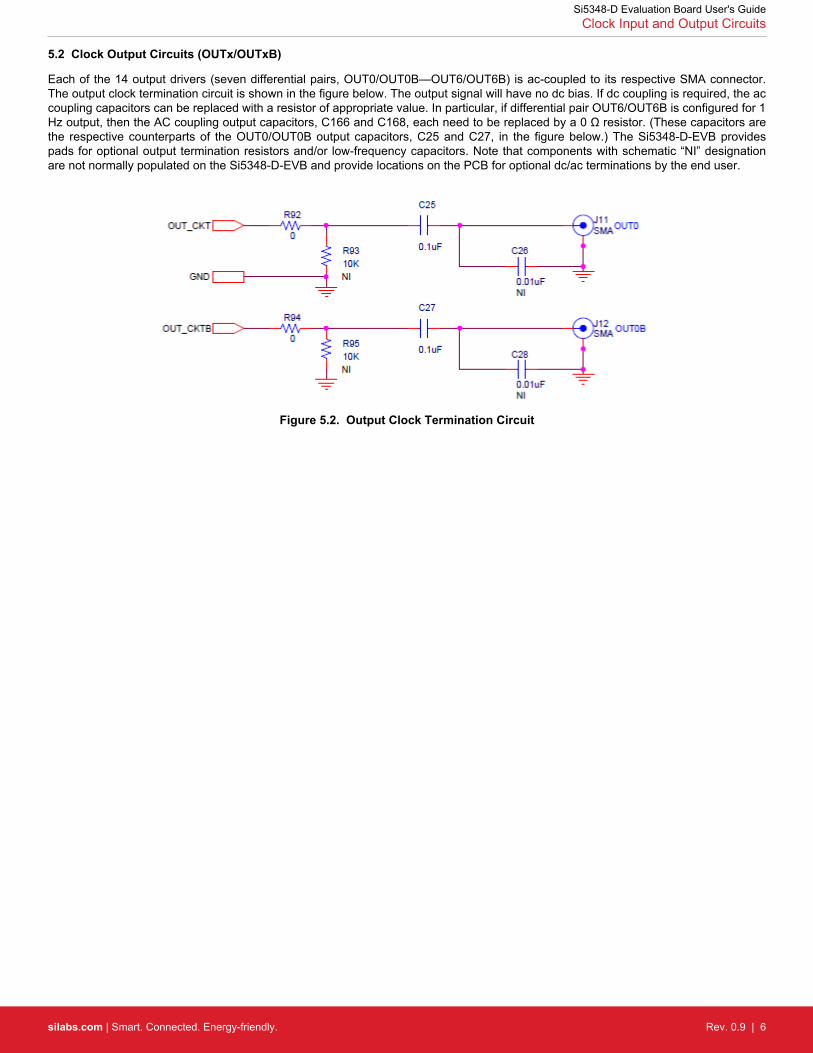
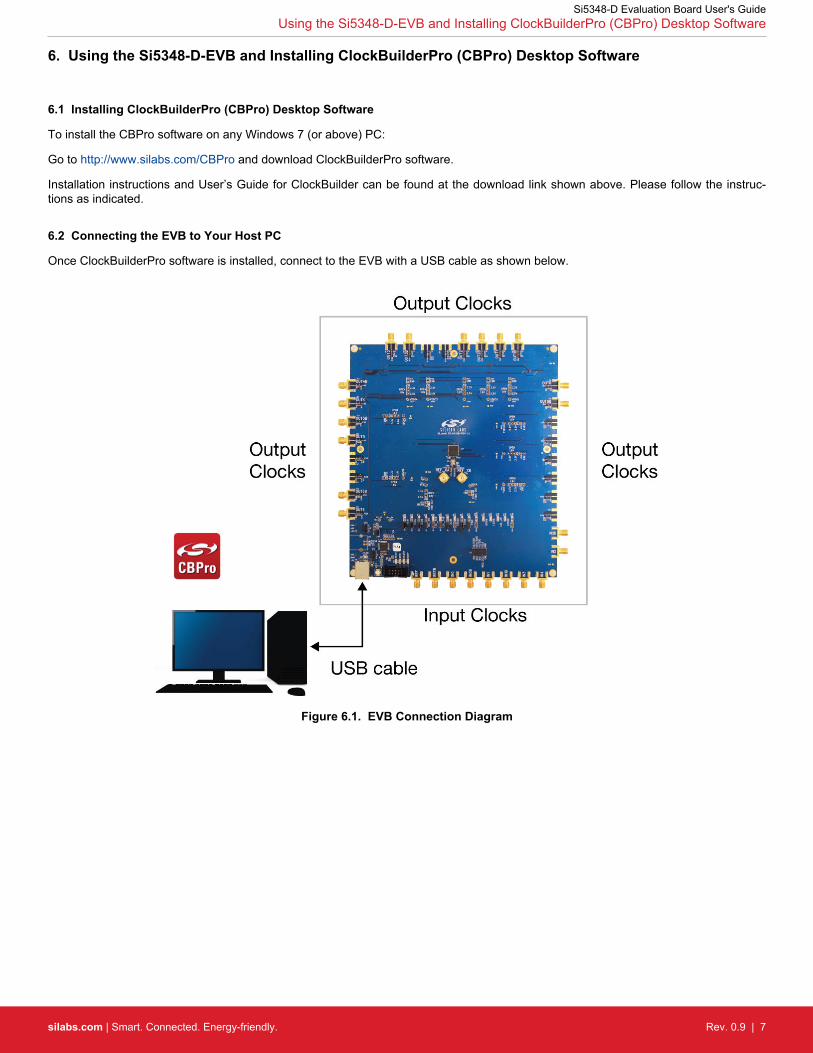
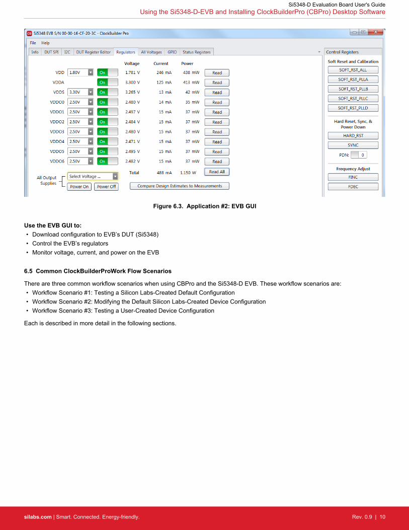
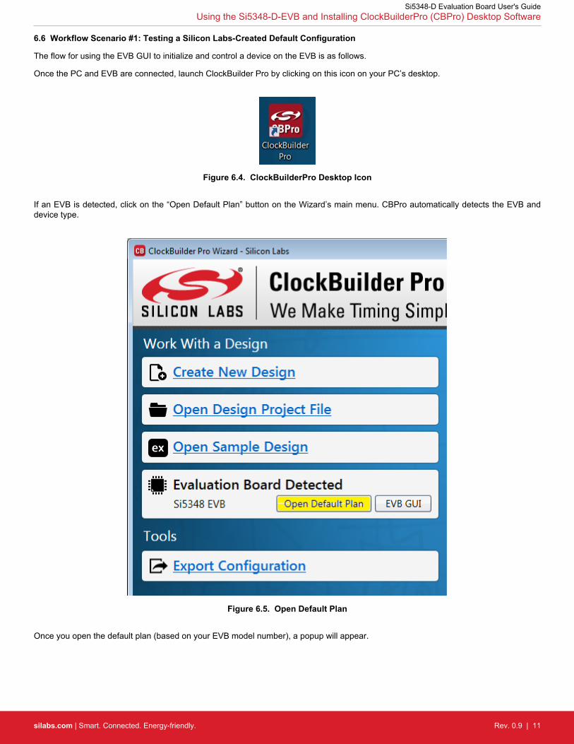
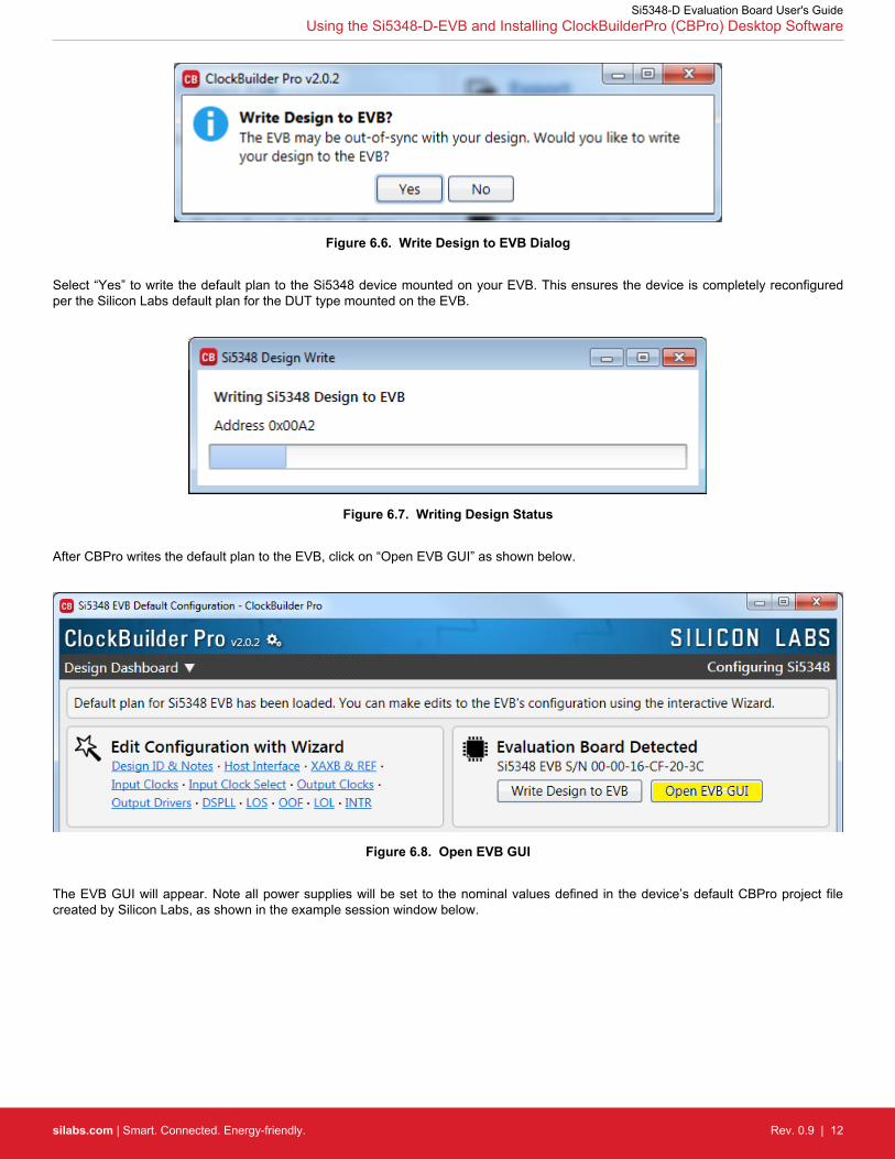
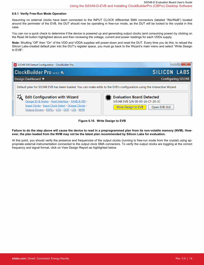
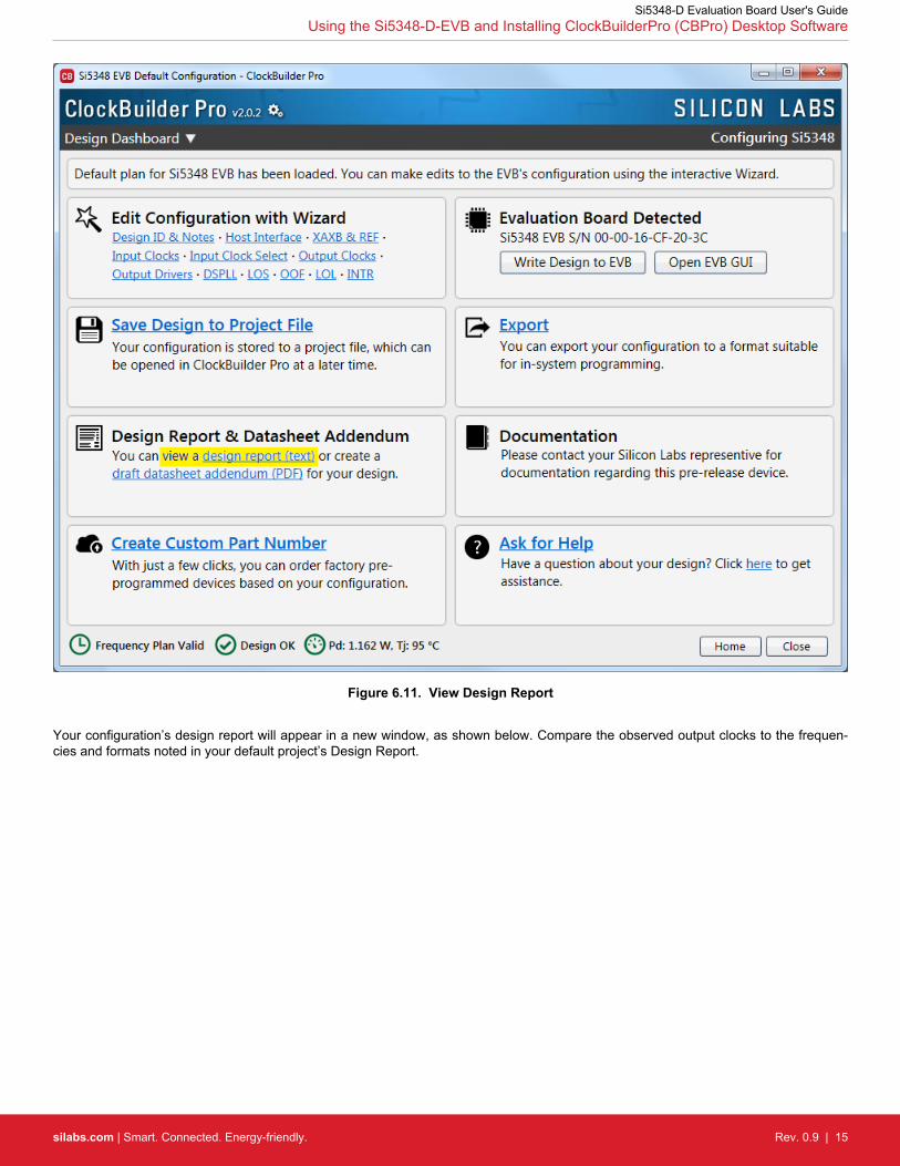
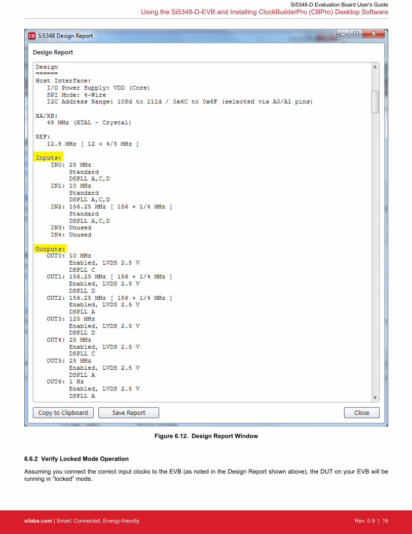
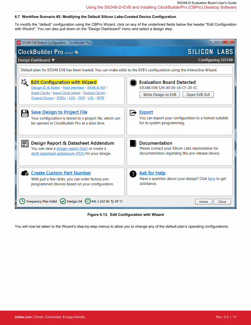
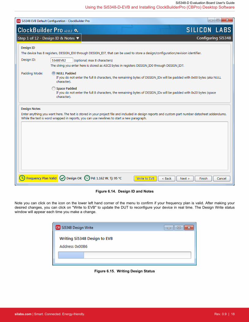
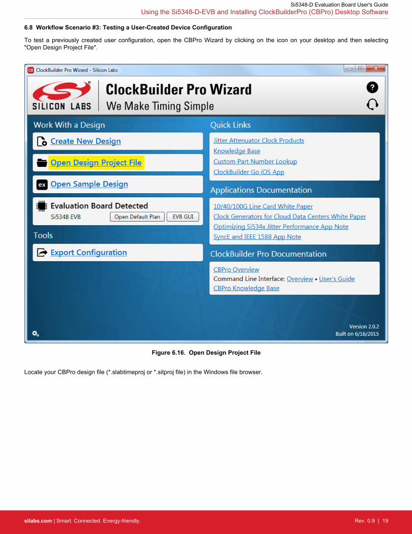
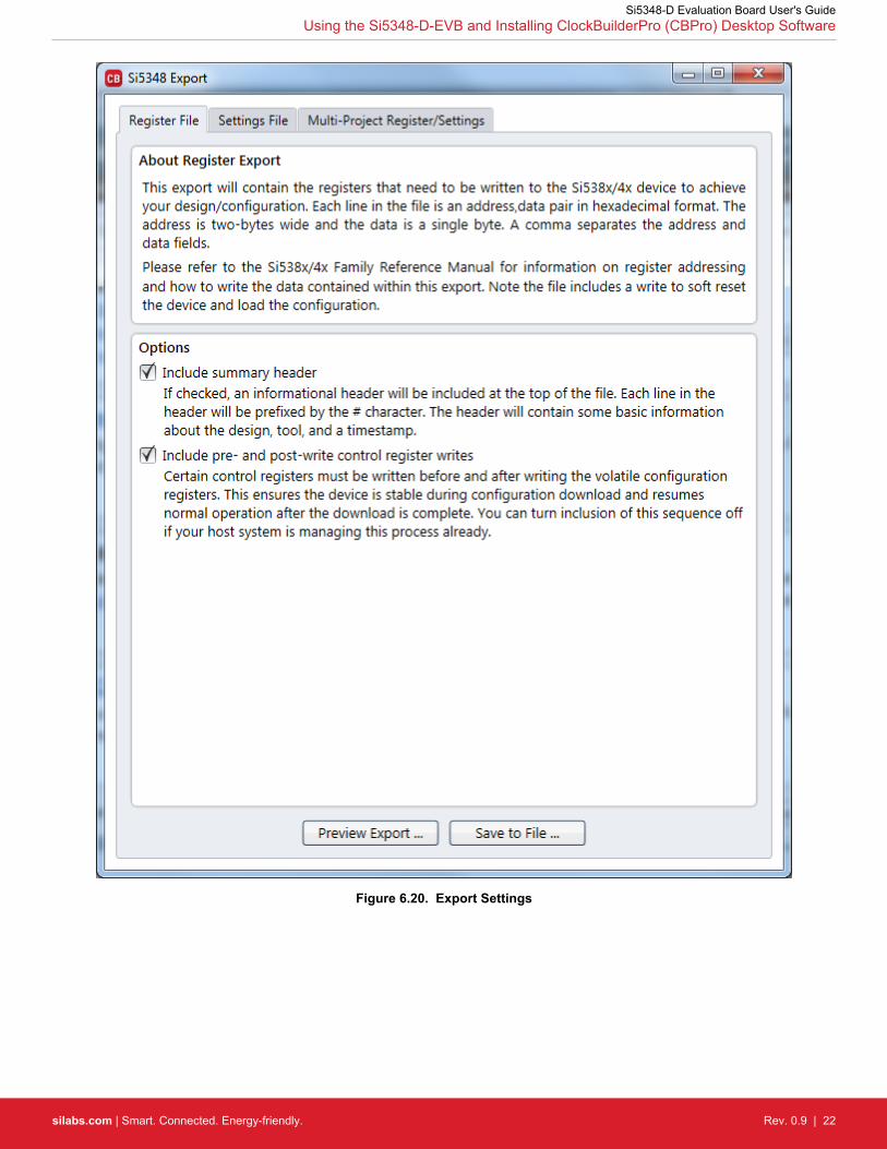