Embed Size (px)
Citation preview

© NOKIA syntsat.PPT / 15.1.1999 / Kalle Asikainen page: 1
Frequency synthesis a in mobile phoneFrequency synthesis a in mobile phone
Kalle Asikainen
NMP
Tampere

© NOKIA syntsat.PPT / 15.1.1999 / Kalle Asikainen page: 2
The local oscillator in a radio transceiverThe local oscillator in a radio transceiver
• The local oscillator (LO) is needed in every radio transceiver irrespective of the RFarchitecture
• The LO is used to mix the wanted frequency down to IF (or baseband) and viceverse
• The LO has to be tunable across the wanted frequency band and the frequencyresolution has to be equal to the channel spacing.
• This kind of LO is called frequency synthesizer!frequency synthesizer!• In a superheterodyne transceiver there are several LO:s and thus several frequency
synthesizers
• In microvawe radio at least one LO is running at microwave frequency
2nd LO
2nd IFRF_Filter_1 2nd Mixer
Demodulator
Antenna
1st Mixer
1st LO
1st IFLNA RF_Filter_2
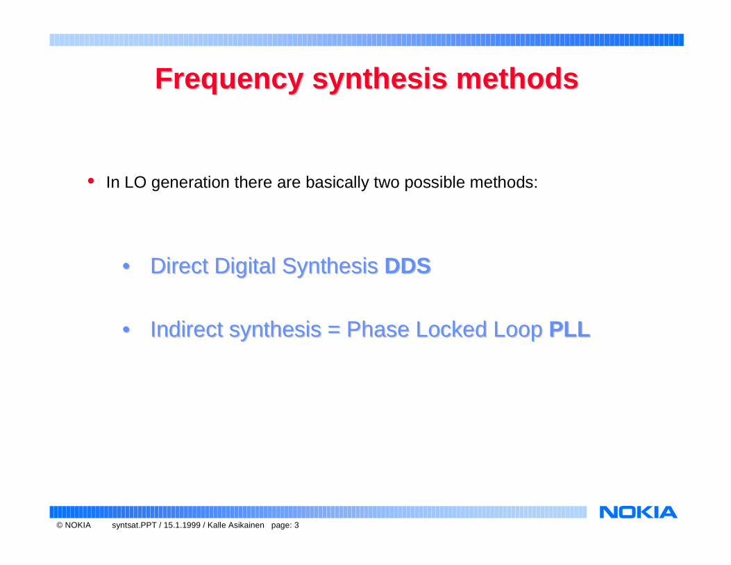
© NOKIA syntsat.PPT / 15.1.1999 / Kalle Asikainen page: 3
Frequency synthesis methodsFrequency synthesis methods
• In LO generation there are basically two possible methods:
•• Direct Digital Synthesis Direct Digital Synthesis DDSDDS
•• Indirect synthesis = Phase Locked Loop Indirect synthesis = Phase Locked Loop PLLPLL

© NOKIA syntsat.PPT / 15.1.1999 / Kalle Asikainen page: 4
Direct digital synthesis DDSDirect digital synthesis DDS
• Digital samples of sinewaves of different frequencies are converted to analog by
DAC and often mixed with additional LO to RF/ microwave band
+ Immediate settling to frequency hop
- Spurioses
- Power consumption
- Needs extra LO and mixer to cover RF/microwave frequencies
• At the moment not very practical for a mobile phone !
• Used in base stations (fast settling time) and signal generators/spectrumanalysers

© NOKIA syntsat.PPT / 15.1.1999 / Kalle Asikainen page: 5
Indirect synthesisIndirect synthesis = PLL
• RF/microwave frequency is generated by multiplying a stable referencefrequency
• PLL is used as a multiplier
+ Small power consumption
+ Spurioses controllable by PLL design
- Settling time limited by control theory !
• The most widely used LO generation method in all kinds of different transceivers

© NOKIA syntsat.PPT / 15.1.1999 / Kalle Asikainen page: 6
PLL synthesizer basicsPLL synthesizer basics
• The phase detector PD compares the reference frequency to the frequency from afeedback divider N
• PD controls the frequency of a voltage controlled oscillator VCO according to thephase/frequency difference of its inputs
• The output of the PD is pulsed and is translated to dc by the action the of loop filter
• The VCO frequency is divided back down to reference frequency by N divider
• By changing the N divider the output frequency can be controlled
• The output frequency resolution equals reference frequency (channel spacing)
Divider
Loop filter
PhaseDetector
Reference freq
Output

© NOKIA syntsat.PPT / 15.1.1999 / Kalle Asikainen page: 7
What is a control system ?What is a control system ?
Controlled systemor plant
Controller
Controlforces
DisturbancesReferencecommands
Output orcontrolledvariables
© NOKIA syntsat.PPT / 15.1.1999 / Kalle Asikainen page: 8
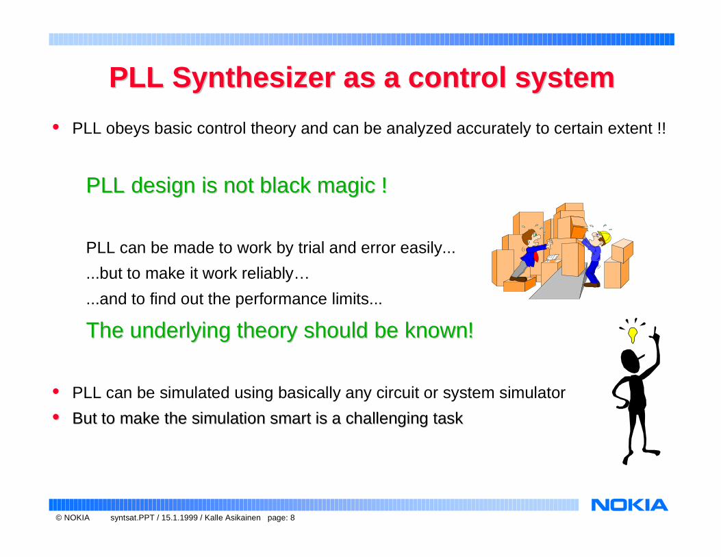
PLL Synthesizer as a control systemPLL Synthesizer as a control system
• PLL obeys basic control theory and can be analyzed accurately to certain extent !!
PLL design is not black magic !PLL design is not black magic !
PLL can be made to work by trial and error easily...
...but to make it work reliably…
...and to find out the performance limits...
The underlying theory should be known!The underlying theory should be known!
• PLL can be simulated using basically any circuit or system simulator
•• But to make the simulation smart is a challenging taskBut to make the simulation smart is a challenging task

© NOKIA syntsat.PPT / 15.1.1999 / Kalle Asikainen page: 9
Synthesizer as a sampled systemSynthesizer as a sampled system
• Due to sampled nature of the phase detector and the loop divider the loop cannot betreated as a continuous time system in it’s strictest sense
• In addition to that all the loop components e.g. phase detector and VCO are notexactly linear
• Still if the loop bandwidth is less than tenth of the phase detector sampling frequencyand all the components can be approximated by linear functions the continuos timeLaplace domain representation can be used
• If the loop BW gets closer to the phase detector sampling frequency the discrete timeeffects should be taken into account in order to to get accurate simulation results
• The discrete time z-domain analyses should be used
• The sampling introduces inherent sampling delay which tends to decrease phasemargins compared to continuos time analyzes
• Sampling also causes aliasing of the noise at the offset of sampling frequency to thebaseband frequencies

© NOKIA syntsat.PPT / 15.1.1999 / Kalle Asikainen page: 10
Basic PLL control system inBasic PLL control system in Laplace Laplacedomaindomain
Ko / sF(s)Kd+Θr s( ) Θo s( )
1/N
V sd ( ) V sc ( )
Θ f s( )
Θe s( )
s
sFKKsG od
fwd
)()( =
sN
sFKKsG od
ol
)()( =
N
sFKKs
sFKK
sG
sG
s
ssH
od
od
ol
fwd
r
o
)()(
)(1
)(
)(
)()(
+=
+=
ΘΘ=
Forward gainForward gainOpen loop gainOpen loop gain
Closed loop transfer function Closed loop transfer function

© NOKIA syntsat.PPT / 15.1.1999 / Kalle Asikainen page: 11
Order of the control systemOrder of the control system
• The order of the system refers to the highest degree of the polynomial expression
• Which is called the Characteristic Equation (C.E.)
• The roots of the C.E. become the closed-loop poles of the overall transfer functionH(s)
• Even the simplest PLL is of second order, but in practice they are of 3rd to 5th order
ECGol .01 ≅=+
N
sFKKs
sFKK
sG
sG
s
ssH
od
od
ol
fwd
r
o
)()(
)(1
)(
)(
)()(
+=
+=
ΘΘ=
© NOKIA syntsat.PPT / 15.1.1999 / Kalle Asikainen page: 12
• The type of a system refers to the number of poles of the open-loop gain Gol(s)located at the origin.
• In other words, it tells how many perfect integratorsperfect integrators there exists in the loop.
• The VCO in a PLL introduces one perfect integrator
• Because the phase of the VCO is linearly related to the integral of the controlvoltage
• To enhance the tracking capability of the PLL the additional integrator is necessaryi.e. Type II PLL is often wanted
• Type II loop is capable of tracking the phase error to zero in case of a frequencystep
• The additional integrator is implemented in a loop filter
• In the past the active loop filters were used
• Nowadays phase detector with charge pump (current) output combined with asimple passive loop filter serves the same purpose
Type of the control systemType of the control system

© NOKIA syntsat.PPT / 15.1.1999 / Kalle Asikainen page: 13
Closed loop response (Transfer response)Closed loop response (Transfer response)
• Closed loop response has a low pass nature
• It shows how the noise from the reference or the phase detector is handled by theloop
• The reference noise is multiplied by N2 within the loop BW and shaped by the closedloop response of the PLL
2
2
2
2
)(1
)()(
)(
sFKK
sN
N
N
sFKKs
sFKKsH
od
od
od
+
=+
=
100.0 300.0 1.0k 3.0k 10.0k 30.0k 100.0k300.0k44.00
54.00
64.00
74.00
84.00
-30.00
-20.00
-10.00
0.00
10.00APLAC 7.02 User: Nokia Corporation Nov 05 1998
PLL closed loop freq response
out
[dB]
f [Hz]
err
[dB]
|out| |err||out| |err|
Blue curve is a closed loop responseBlue curve is a closed loop response

© NOKIA syntsat.PPT / 15.1.1999 / Kalle Asikainen page: 14
Error transfer responseError transfer response
• Error transfer response E(s) is the response from PD reference input to PD output
• The response from the VCO control voltage Vc(s) to VCO output frequency sΘo(s)(remember that frequency is the time derivate of the phase) has the same responsebut multiplied by VCO gain
• It is often called modulation response M(s) as it tells about the PLL:s capabilityto suppress the modulation inserted to VCO
• Error transfer response has a high pass nature
N
sFKKs
s
sN
sFKKs
ssE
ododr
e
)()(1
1
)(
)()(
+=
+=
ΘΘ=
100.0 300.0 1.0k 3.0k 10.0k 30.0k 100.0k300.0k44.00
54.00
64.00
74.00
84.00
-30.00
-20.00
-10.00
0.00
10.00APLAC 7.02 User: Nokia Corporation Nov 05 1998
PLL closed loop freq response
out
[dB]
f [Hz]
err
[dB]
|out| |err||out| |err|
Green curve is an error transfer responseGreen curve is an error transfer response
N
sFKKs
sK
sN
sFKKK
sV
ss
sV
sfsM
od
o
od
o
c
o
c
o
)()(1)(
)(
)(
)()(
+=
+=Θ==

© NOKIA syntsat.PPT / 15.1.1999 / Kalle Asikainen page: 15
Phase marginPhase margin
• The Bode plot is a useful tool for analyzing the stability of the control system. Itconsists of a pair of graphs displaying the polar components of the open-loop gainGol(s) as a function of the frequency.
• If Gol(s)= 0dB at the same time when ∠Gol(s) = -180° this equals to Gol(s) = -1
• In these conditions the denominator of the loop transfer function H(s) equals zeromaking the loop unstable
• Phase margin tells how far the design is from the instability, usual goal being 45°
100.0 300.0 1.0k 3.0k 10.0k 30.0k 100.0k300.0k-10.00
0.00
10.00
20.00
30.00
-180.0
-90.00
0.00
90.00
180.0APLAC 7.02 User: Nokia Corporation Nov 05 1998
PLL open loop freq response
|G|
[dB]
f [Hz]
/_G
[°]
|G| /_G|G| /_G
)(1
)(
)(
)()(
sG
sG
s
ssH
ol
fwd
r
o
+=
ΘΘ=

© NOKIA syntsat.PPT / 15.1.1999 / Kalle Asikainen page: 16
Peaking and phase marginPeaking and phase margin
H ω ζ,( )N 2 ζ. ω n
. j. ω. ω n2.
j ω.( )2
j ω. 2. ζ. ω n. ω n
2 N 10
dB H ω 0.1,( )( )
dB H ω 0.3,( )( )
dB H ω 0.5,( )( )
dB H ω 0.7,( )( )
dB H ω 1,( )( )
dB H ω 1.5,( )( )
ωω n
0.1 1 106
12
18
24
30
36Loop transfer response
The plot shows the second order system transfer response with different damping factorsThe plot shows the second order system transfer response with different damping factors (damping factor is a measure of stability and corresponds to the phase margin (damping factor is a measure of stability and corresponds to the phase margin
of the higher order system) of the higher order system)
The peaking of the loop response depends on the phase margin of the loopThe peaking of the loop response depends on the phase margin of the loop

© NOKIA syntsat.PPT / 15.1.1999 / Kalle Asikainen page: 17
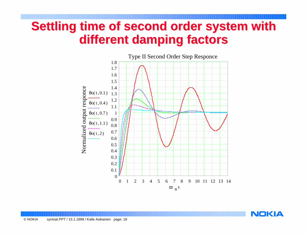
Synthesizer settling timeSynthesizer settling time
• When N divider is changed the step like frequency error is seen between the phasedetector inputs
• The wider the loop BW the faster the settling time
• The optimum phase margin from settling time point of view is about 45 - 50 degreesgiving overshoot of step response of about 30-35%
• With smaller phase margin the ringing of the step response slowers the settlingconsiderably
0.000 125.00u 250.00u 375.00u 500.00u0.00
20.00M
40.00M
60.00M
80.00M
-1.00
-0.50
0.00
0.50
1.00APLAC 7.02 User: Nokia Corporation Nov 05 1998
PLL loop step response
f
[Hz]
t [s]
pha
[rad]
N*f_in ph_errf_out
N*f_in ph_errf_out
0.000 125.00u 250.00u 375.00u 500.00u-20.00
-10.00
0.00
10.00
20.00
-200.0
-100.0
0.00
100.0
200.0APLAC 7.02 User: Nokia Corporation Nov 05 1998
PLL loop output phase error
t [s]
f_err
[Hz]
ph_err freq_errph_err freq_err
© NOKIA syntsat.PPT / 15.1.1999 / Kalle Asikainen page: 18
Settling time of second order system withSettling time of second order system withdifferent damping factorsdifferent damping factors
θo t 0.1,( )
θo t 0.4,( )
θo t 0.7,( )
θo t 1.1,( )
θo t 2,( )
ω n t.0 1 2 3 4 5 6 7 8 9 10 11 12 13 14
00.1
0.20.3
0.40.5
0.60.7
0.80.9
11.1
1.21.31.41.5
1.6
1.71.8
Type II Second Order Step Responce
Nor
mal
ized
out
put r
espo
nce

© NOKIA syntsat.PPT / 15.1.1999 / Kalle Asikainen page: 19
Settling time measured with modulationSettling time measured with modulationdomain analyzer MDAdomain analyzer MDA

© NOKIA syntsat.PPT / 15.1.1999 / Kalle Asikainen page: 20
ReferenceReference spurioses spurioses
• The operation of the phase detector is repetitious at the reference frequency
• The loop filter can newer filter the reference frequency completely out
• The remaining ac modulates the VCO generating so called reference spurioseswhich can be seen at the VCO spectrum as discrete spikes
• Spurious signals are expressed as relative to the carrier power dBc
• The most problematic about the reference spurioses is that they fall to adjacentchannels of the communications system
• Any dc current leakage in the loop filter will increase spurioses because the lostcontrol voltage has to be compensated by the phase detector pulses
• The highest attenuation of the reference spurioses is obtained when:
• the loop BW is narrow
• the phase margin is small => high peaking gives fast roll-off
• the loop is of high order (several poles at the same frequency range give fasterroll-off)

© NOKIA syntsat.PPT / 15.1.1999 / Kalle Asikainen page: 21
ReferenceReference spurioses spurioses measured with measured withspectrum analyzerspectrum analyzer
© NOKIA syntsat.PPT / 15.1.1999 / Kalle Asikainen page: 22
Phase noisePhase noise
• The signal is in general case given by
• where A(t) represents the time dependent amplitude and θ(t) the time dedentphase
• In synthesizer A(t) is often taken to be constant which means that no AMmodulation or amplitude noise is present
VCO has an amplitude limiting property
phase detector and dividers are only sensitive to phase
• That’s why the phase modulation (noise) θ(t) is usually the only noise present ina synthesizer
• The most commonly used phase noise notation a so called SSB (single sideband)phase noise L(f) which is a ratio of power spectral density in one phase modulationsideband to the total signal power. The unit of L(f) is dBc/Hz.
• It can be measured using spectrum analyzer which gives two-sided spectrum(there seems to be contradiction in terms: SSB spectrum is two sided)
• When the noise is measured using SA the resolution bandwidth has to be takeninto account (the real value referred to 1Hz band is 10*log(RBW) lower than themeasured noise)
[ ])(cos)()( 0 tttAtS θω +=
© NOKIA syntsat.PPT / 15.1.1999 / Kalle Asikainen page: 23
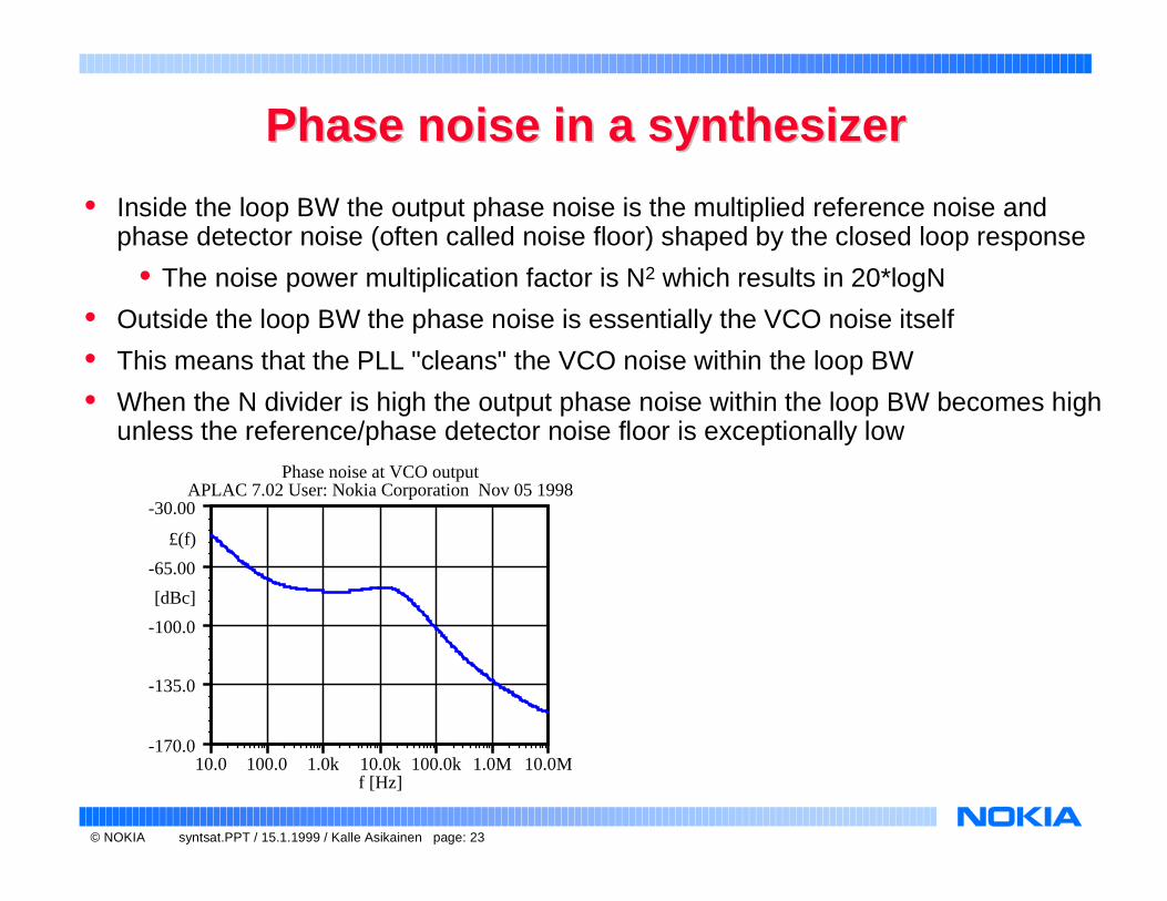
Phase noise in a synthesizerPhase noise in a synthesizer
• Inside the loop BW the output phase noise is the multiplied reference noise andphase detector noise (often called noise floor) shaped by the closed loop response
• The noise power multiplication factor is N2 which results in 20*logN
• Outside the loop BW the phase noise is essentially the VCO noise itself
• This means that the PLL "cleans" the VCO noise within the loop BW
• When the N divider is high the output phase noise within the loop BW becomes highunless the reference/phase detector noise floor is exceptionally low
10.0 100.0 1.0k 10.0k 100.0k 1.0M 10.0M-170.0
-135.0
-100.0
-65.00
-30.00APLAC 7.02 User: Nokia Corporation Nov 05 1998
Phase noise at VCO output
£(f)
[dBc]
f [Hz]
© NOKIA syntsat.PPT / 15.1.1999 / Kalle Asikainen page: 24
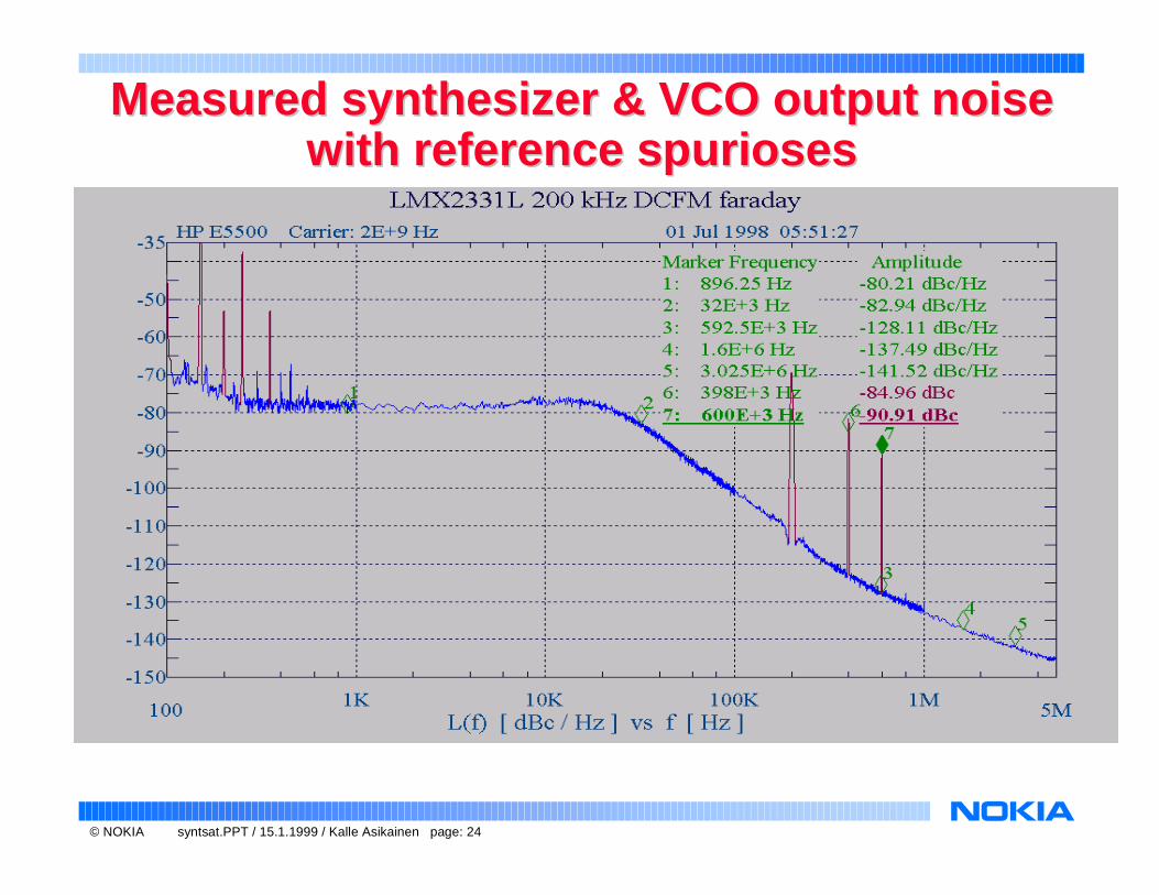
Measured synthesizer & VCO output noiseMeasured synthesizer & VCO output noisewith referencewith reference spurioses spurioses

© NOKIA syntsat.PPT / 15.1.1999 / Kalle Asikainen page: 25
Synthesizer output noise measured with aSynthesizer output noise measured with aspectrum analyzer (linear frequency scale)spectrum analyzer (linear frequency scale)
© NOKIA syntsat.PPT / 15.1.1999 / Kalle Asikainen page: 26
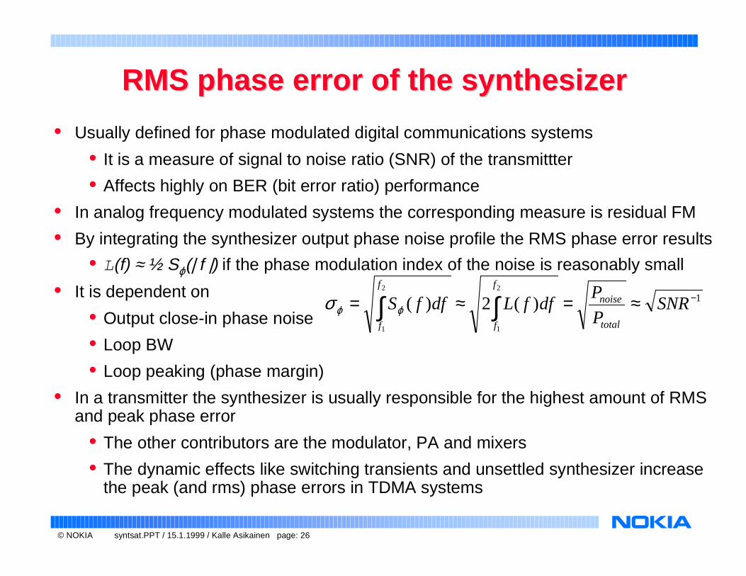
RMS phase error of the synthesizerRMS phase error of the synthesizer
• Usually defined for phase modulated digital communications systems
• It is a measure of signal to noise ratio (SNR) of the transmittter
• Affects highly on BER (bit error ratio) performance
• In analog frequency modulated systems the corresponding measure is residual FM
• By integrating the synthesizer output phase noise profile the RMS phase error results
• L(f) ≈ ½ Sϕ(| f |) if the phase modulation index of the noise is reasonably small
• It is dependent on
• Output close-in phase noise
• Loop BW
• Loop peaking (phase margin)
• In a transmitter the synthesizer is usually responsible for the highest amount of RMSand peak phase error
• The other contributors are the modulator, PA and mixers
• The dynamic effects like switching transients and unsettled synthesizer increasethe peak (and rms) phase errors in TDMA systems
12
1
2
1
)(2)( −≈=≈= ∫∫ SNRP
PdffLdffS
total
noise
f
f
f
f
ϕϕσ
© NOKIA syntsat.PPT / 15.1.1999 / Kalle Asikainen page: 27
Phase detector = PDPhase detector = PD
• There exists multiplier type (mixer) PD:s and a variety of different sample&hold PD:s
• The most commonly used PD is though a so called PFD Phase Frequency Detector
• Its has an infinite lock-in range and ±2π linear range
• PFD is normally followed by current source charge pump
• Current output gives the better linearity than voltage output
• Additional integrator required by Type II loop can be realized by a simple passiveloop filter
• Phase detector gain is related to the output current
• Phase detector should have extremely low noise floor
• The noise floor depends on the sampling frequency (reference frequency) anddetector gain (current)
higher sampling frequency gives higher noise floor
higher charge pump current gives usually lower noise floor
• In GSM type of solutions the noise floor should be around -150...-160dBc/Hz
π2o
d
IK =

© NOKIA syntsat.PPT / 15.1.1999 / Kalle Asikainen page: 28
PFD responsePFD response
π �π �π �π�π��π��π��π
�9G
�9G

© NOKIA syntsat.PPT / 15.1.1999 / Kalle Asikainen page: 29
Simple Phase Frequency Detector PFD Simple Phase Frequency Detector PFD
D
Q
Q
CK
SET
CLR
U
D
"1"
"1"
Ref
VCO
D
Q
Q
CK
SET
CLR
R
R

© NOKIA syntsat.PPT / 15.1.1999 / Kalle Asikainen page: 30
PFD with current source charge pumpPFD with current source charge pumpoutputoutput
Charge pump is followed by simple filter which has Charge pump is followed by simple filter which has an integrator response when the input is current an integrator response when the input is current
sCR
sC
sRC
sI
sVsF
11
)(
)()( +=+==
© NOKIA syntsat.PPT / 15.1.1999 / Kalle Asikainen page: 31
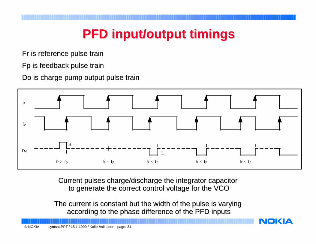
PFD input/output timingsPFD input/output timings
fr
fp
fr > fp fr = fp fr < fp fr < fp fr < fp
D o
H
L
Fr is reference pulse trainFr is reference pulse train
Fp is feedback pulse trainFp is feedback pulse train
Do is charge pump output pulse trainDo is charge pump output pulse train
Current pulses charge/discharge the integrator capacitor Current pulses charge/discharge the integrator capacitor to generate the correct control voltage for the VCOto generate the correct control voltage for the VCO
The current is constant but the width of the pulse is varying The current is constant but the width of the pulse is varying according to the phase difference of the PFD inputsaccording to the phase difference of the PFD inputs

© NOKIA syntsat.PPT / 15.1.1999 / Kalle Asikainen page: 32
Second order loop filter for charge pumpSecond order loop filter for charge pumpPFDPFD
C2
R2
I(s) V(s)
C1
)(
1
)(
)()(
21221
22
CCRCsCs
RsC
sI
sVsF
+++==
21
2121 CC
CCR
+=τ
The first pole is at the origin (integrator)The first pole is at the origin (integrator)
The second pole has a time constantThe second pole has a time constant
τ2 = R2C2The zero has a time constantThe zero has a time constant
The filter response can be written in the formThe filter response can be written in the form
211
12
)1(
)1()(
ττττCss
ssF
++=

© NOKIA syntsat.PPT / 15.1.1999 / Kalle Asikainen page: 33
Transfer function of second order loop filterTransfer function of second order loop filter
C1 0.6810 9. C2 3.310 9. R2 3.9103.
F ω( )j ω. R2. C2. 1( )
j ω. C1 C2 j ω. C2. R2. C1.( ).( )
dB Mag F ω x( )( )( )( )
ω x( )
2 π.
10 100 1 103
1 104
1 105
1 106
1 107
1 108
0
30
60
90
120
150Transfer function of loop filter
Ph F ω x( )( )( )
ω x( )
2 π.
10 100 1 103
1 104
1 105
1 106
1 107
1 108
135
90
45
0Phase response of transfer function

© NOKIA syntsat.PPT / 15.1.1999 / Kalle Asikainen page: 34
4th order loop filter for charge pump PFD4th order loop filter for charge pump PFD
C2
R2
I(s) R3 V(s)
C1 C3 C4
R4
Additional poles have time constants Additional poles have time constants τ3 = R3C3
τ4 = R4C4
Additional poles have to be at high enough frequency not to ruin the phase marginAdditional poles have to be at high enough frequency not to ruin the phase margin
© NOKIA syntsat.PPT / 15.1.1999 / Kalle Asikainen page: 35
Reference sourceReference source
• Is typically a VCTCXO Voltage Controlled Temperature Compensated CrystalOscillator
• Has to have a high frequency stability (temperature compensated)
• GSM spec 0.1ppm (parts per million)
• Has to have low phase noise, in GSM -120…-145dBc/Hz at 1kHz offset
• Because the reference noise is increased by 20*logN by the PLL
• Is normally voltage controlled in order to AFC Automatic Frequency Control to beable to tune the local oscillator according to temperature changes and Doppler shift
• Crystal oscillator typically operates at several MHz and has to be divided down toreference frequency (channel spacing)
• The reference divider is usually called R divider
• The division by R decreases the phase noise by 20*logR, which has to be takeninto account when calculating the noise budget of the synthesizer

© NOKIA syntsat.PPT / 15.1.1999 / Kalle Asikainen page: 36
VCOVCO
• Linear tuning range has to cover the operating band
• VCO gain Ko (tuning sensitivity) is expressed in MHz/V
• Phase noise spec is typically deduced from rms phase error spec (= noise floor andloop BW) at low offsets and blocking spec at high offsets
• An important specs in TDMA systems are pushing and pulling figures
• Pushing tells the frequency change as a function of the source voltage change(source glitch or ground bounce)
• Pulling tells the frequency change as a function of the load change
• Low battery voltages in current and future mobile phones causes certain problems:
• Wide tuning range combined with low source voltage makes the VCO gain high
• High gain makes the pushing figure and phase noise worse
• This can be solved by using higher voltage source for PLL charge pump in orderto get the VCO gain lower
• Low power consumption tends to rise the phase noise because the energy stored ina resonator circuit is smaller

© NOKIA syntsat.PPT / 15.1.1999 / Kalle Asikainen page: 37
Feedback (N) dividerFeedback (N) divider
• N divider has to be programmable in order to change the output frequency
• At RF/Microwave frequencies the special prescaler P (often BJT) is used beforeprogrammable divider in order to bring the frequency low enough for standard CMOSlogic to handle
• The fixed prescaler would make the minimum step of the divider equal to prescalingfactor
• This can be overcome by a so called dual modulus prescaler P/(P+1) where twoprescaling factors are alternated by the following CMOS logic
• The input is divided by (P+1) for A times and by P for (B-A) times thus giving the totaldivision ratio of the dual-modulus prescaler of:
• Ntot = A(P+1) + (B-A)P = BP + A, where B ≥ A
• The smallest possible division ratio of a dual modulus prescaler is P2
• In order to accomplish smaller minimum division ratios the three- or even four-modulus (quad-modulus) prescalers are sometimes used

© NOKIA syntsat.PPT / 15.1.1999 / Kalle Asikainen page: 38
Dual modulusDual modulus prescaler prescaler
P/(P+1)
B
A
logic
modulus control
outputinput
load
load
A
B
Dual-modulus prescaler

© NOKIA syntsat.PPT / 15.1.1999 / Kalle Asikainen page: 39
The limitations of integer N dividerThe limitations of integer N divider
• In integer-N synthesizers the channel spacing dictates the reference frequencybecause the output frequency can only be an integer multiple of reference
• As the loop filter should be able to attenuate the reference spurs to the specifiedlevel the bandwidth of the loop should be comparable to the reference frequency
• This of course sets the limit for the realizable settling time
• 20*logN noise multiplication sets the amount of phase noise at the output caused bythe noise floor of the synthesizer.
• This means that if the channel spacing is small and at the same time the outputfrequency is high it is practically impossible to design a synthesizer with a smallrms phase error.
• The obvious solution to previous problems seems to be an N divider capable offractional division !

© NOKIA syntsat.PPT / 15.1.1999 / Kalle Asikainen page: 40
Fractional-N dividerFractional-N divider
• N divider that is capable of dividing by fractional division ratio instead of only byinteger division ratio.
• This way the reference frequency can be higher than the channel spacing.
• Reference spurioses move to higher offsets (easier to filter out by the loop filter)
• Noise multiplication by 20*logN gets smaller
• Actually digital divider capable of fractional division does not exist but it has to beimplemented by alternating two (or more) different division ratios
• Fractional-N synthesizers are based on conventional synthesizer design, but with anadditional control circuitry to rapidly alternate the division ratio between N and (N+1)
• Let us assume that the feedback divider ratio is N for (q - p) reference periods and(N+1) for p reference periods. Over the q reference periods, the average outputfrequency is
• The concept is quite similar to the dual-modulus counters. In fractional-N the periodof dual modulus operation extends over more than one reference period whereas inan integer N the dual-modulus operation is reduced within one reference period only
( ) ( )
+=
++−=q
pNf
q
pNpqNf refref
1fout
© NOKIA syntsat.PPT / 15.1.1999 / Kalle Asikainen page: 41
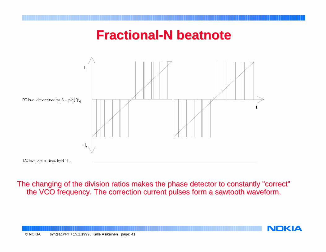
Fractional-NFractional-N beatnote beatnote
W
'&�OHYHO�GHWHUPLQHG�E\��1���S�T�� IUHI�
'&�OHYHO�GHWHUPLQHG�E\�1� �IUHI
,R
��,R
The changing of the division ratios makes the phase detector to constantly "correct" The changing of the division ratios makes the phase detector to constantly "correct" the VCO frequency. The correction current pulses form a sawtooth waveform. the VCO frequency. The correction current pulses form a sawtooth waveform.

© NOKIA syntsat.PPT / 15.1.1999 / Kalle Asikainen page: 42
Fractional N compensationFractional N compensation
• The fractional sawtooth (beatnote) modulates the VCO generating the so calledfractional sidebands
• They fall to adjacent channel frequencies as in integer N synthesizer
• Some compensation method is needed to remove the sawtooth
• Fractional N compensation is the heart of the whole fractional N synthesizer
• It defines the performance of the synthesizer !
• The compensation can be made at the output (using DAC) or at the input of thephase detector (using programmable digital delay line DLL)
DLL calibration
4-bit Accum N/N+1 counter
LPF
(LSB) 19-bit RF N register (MSB)
Frefφ
Adderover flow
4-bit F reg 5-bit A reg 10-bit B reg
VCO
D
Compensation scheme at the input of the phase detectorCompensation scheme at the input of the phase detector

© NOKIA syntsat.PPT / 15.1.1999 / Kalle Asikainen page: 43
Fractional-N compensation at the output ofFractional-N compensation at the output ofthe phase detectorthe phase detector
Dual N Divider
Loop filter
PhaseDetector
Xoscillator
Output
$FFXPXODWRU>$@ 'HOD\ '�$
2IIVHW�JDLQ�DGM�
)XOO�DGGHU
9FRPS�W�
Q�ELW
2YHUIORZ
1
1
S� ���WR�T��
IF� ��1���S�T�IUHI
�
9S�W�9UHI�W�
IUHI
9G�W�

© NOKIA syntsat.PPT / 15.1.1999 / Kalle Asikainen page: 44
TheThe uncomplete uncomplete fractional compensation fractional compensationeffectseffects
• Unfortunately neither of the compensation methods can do the job properly
• Fractional spurious compensation is usually not perfect
• In some bad designs they can still be as high as in integer N synthesizer
• In this case the wider loop BW than in integer N cannot be used
• In all designs fractional compensation tends to rise the phase detector noise floor
• In some bad designs the noise floor rise can mask the noise multiplication benefitof smaller N divider figure
• From this perspective it would be more efficient to prevent the generation ofspurioses rather than compensating them
• A third compensation method that actually combines the fractionality generatorand the spurious compensation is utilizing noise shaping ∆Σ modulator as acontroller for the multimodulus divider
• Using this method very small frequency resolution can be realized
• Excellent close in phase noise performance can be reached but the phase noiseat high offsets (outside loop BW) can be rather high due to high pass noiseshaping

© NOKIA syntsat.PPT / 15.1.1999 / Kalle Asikainen page: 45
Fractional-N generation/compensationFractional-N generation/compensationusing using ∆Σ∆Σ modulator modulator
PFDfref VCO
N / ...N+2p-1
fout
∆Σ P control bitsfrequency control
F(s)

© NOKIA syntsat.PPT / 15.1.1999 / Kalle Asikainen page: 46
Fractional-N applicationsFractional-N applications
• Despite it’s trade offs fractional-N synthesizers are used in for instance signalgenerators and spectrum analysers where
• Frequency resolution of even sub-herz is needed
• The common claim that fractional-N could improve settling time of the synthesizerconsiderably is missleading
• Statements of lower output noise and lower reference spurioses are notnecessarily true
• It is often said that the faster phase detector uppdate rate would improve settlingtime
• This does not seem to be true
• The benefit is that the continuos time control theory is more valid withhigher phase detector sampling rate (loop BW << fref)
• Nyquist criterium (loop BW < ½ fref) is the ultimate limit of the loop BW !
© NOKIA syntsat.PPT / 15.1.1999 / Kalle Asikainen page: 47
Commercial synthesizer chips for mobileCommercial synthesizer chips for mobilecommscomms
• Usually synthesizer chips consist of:
• Programmable reference divider R
• PFD phase detector followed by charge pump with programmable output current
• Dual, triple or quad modulus prescaler followed by programmable divider
= N divider
• Three wire serial programming interface
• Very commonly they include two synthesizers for different frequency bands
• Two locals of superheterodyne transceiver can be generated using onechip
• Still nowadays the external components are typically:
• Reference source (VCTCXO)
• VCO
• Loop filter
• Power supply filtering components

© NOKIA syntsat.PPT / 15.1.1999 / Kalle Asikainen page: 48
Block diagram of typical dual synthesizerBlock diagram of typical dual synthesizer
PHASECOMP.
CHARGEPUMP
Do RF
Do IF
22-BITDATA REGISTER
CLOCK
LE
DATA
Fo/LD
PHASECOMP.
CHARGEPUMP
Fout/
MUX
15-BIT IF
N COUNTERfin IF
18-BIT RFN COUNTERfin RF
OSCOSC in
15-BIT RF R COUNTER Lock
Detect
RFLD
IFLD
15-BIT IF R COUNTER
RFprescalar
IFprescalar

© NOKIA syntsat.PPT / 15.1.1999 / Kalle Asikainen page: 49
About synthesizer specifications 1About synthesizer specifications 1
• Usually selectivity sets most difficult requirement for synthesizer (=VCO) phase noiseat high offsets
• Example GSM 900 small MS (= handportable):
wanted signal 3dB above sensitivity level => -102 dBm + 3 dB = -99 dBm
blocking signal -43 dBm @ 600 kHz offset from the received signal
typical demodulation S/N = 9 dB to meet the BER spec
noise BW = 10*log(200 kHz) = 53dB is the GSM receiver BW
Synthesizer phase noise spec @600KHz offset = -102 - (-43) - 53 - 9 = -121dBc/Hz
Now the noise contribution of the blocking signal is the same as with thermalnoise of the receiver alone (with receiver noise figure NF=10dB) i.e.
-174dBm/Hz + 53dB + 10dB = -111dBm
When two uncorrelated noise sources of -111dBm are present at the sametime the total noise level is -108dBm
Because wanted signal level is -99dBm in blocking conditions the requiredS/N of 9dB is satisfied

© NOKIA syntsat.PPT / 15.1.1999 / Kalle Asikainen page: 50
About synthesizer specifications 2About synthesizer specifications 2
• Example of WCDMA receiver
• blocking signal level -56 dBm @ 10MHz offset from the received signal
typical demodulation S/N= 7 dB for 10-3 BER
noise BW ≈ chip rate = 10*log(3.84MHz) = 66dB in the WCDMA receiver
wanted signal 3dB above the sensitivity level i.e. -117dBm + 3dB = -114dBm
Similarly to GSM example this gives the synthesizer phase noise spec @10MHzoffset = -117 -(- 56) - 66 - 7 = -134dBc/Hz
If the full processing gain of 10log(3.84Mcps/12.2kcps) = 25dB is taken intoaccount the requirement is relaxed to -134dBc/Hz + 25dB = -109dBc/Hz !
• One point worth mentioning is that if synthesizer frequency is double that of LOfrequency the divider by 2 reduces the phase noise theoretically by 6dB. The actualreduction depends on the noise floor of the divider itself compared to the noise levelof the input signal.

© NOKIA syntsat.PPT / 15.1.1999 / Kalle Asikainen page: 51
About synthesizer specifications 3About synthesizer specifications 3
• In GSM the modulation spectrum spec typically sets the most difficult requirement forthe synthesizer reference spurioses
• @ 400kHz offset the modulation spectrum is allowed to have contamination levelof -60dBc measured with 30kHz filter BW
Synthesizer spurious should be < -66dBc @ 400kHz offset
• Usually the selectivity sets synthesizer spurious spec at high offsets
• Example GSM 900 small MS:
wanted signal 3dB above sensitivity level => -102 dBm + 3 dB = -99 dBm
blocking signal -23dBm @ 3MHz offset from the received signal
typical demodulation S/N = 9 dB to meet the BER spec
At least 3dB margin is needed because the phase noise and the receiverthermal noise contribution are present at the same time
Synthesizer spurious spec @ 3MHz offset = -102 - (-23) - 9 - 3 = -91dBc

© NOKIA syntsat.PPT / 15.1.1999 / Kalle Asikainen page: 52
LO phase noiseLO phase noise
• LO mixes both with wantedsignal and interfering signal
• LO spectrum shifts to IF
• LO mixes both with wantedsignal and interfering signal
• LO spectrum shifts to IF
LO RX Interference
IF
IF

© NOKIA syntsat.PPT / 15.1.1999 / Kalle Asikainen page: 53
About synthesizer specifications 4About synthesizer specifications 4
• In GSM the whole transmitter RMS phase error has to be < 5° and peak < 20°
• The rule of thumb is that synthesizer contribution has to be less than half of that
• As an example this can be met if the synthesizer meets approximately thefollowing spec:
• output phase noise is < -74dBc/Hz @ 1kHz offset
• loop BW is < 20kHz with 45° phase margin
• According to WCDMA standard the Error Vector Magnitude (EVM) of the transmitterhas to be < 17.5%
• This equals to RMS phase error of approximately 0.175rad≈ 10°
• From that the synthesizer contribution should be less than half
• The settling time requirement depends on the system and RF architecture
• Typically in GSM phone it is around 500us within ±20Hz
• Some new GSM Phase 2+ features like HSCSD (multislot) and GPRS (packetradio) set much tighter requirements for the settling time
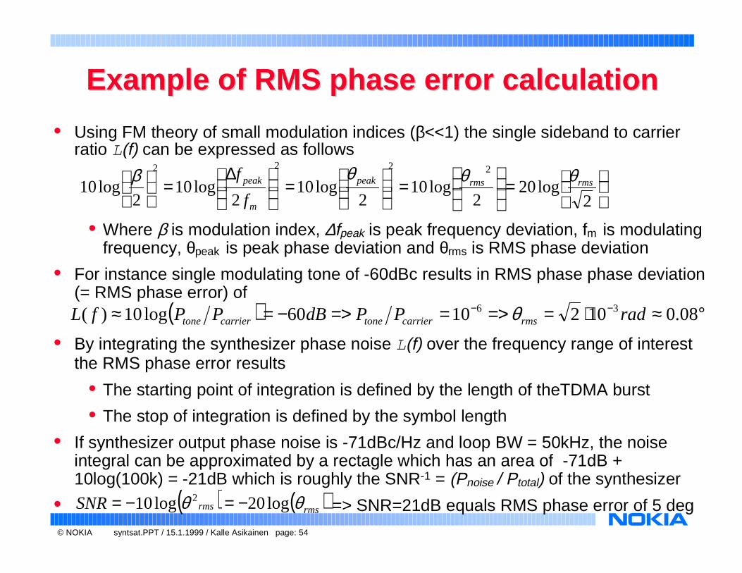
© NOKIA syntsat.PPT / 15.1.1999 / Kalle Asikainen page: 54
Example of RMS phase error calculationExample of RMS phase error calculation
• Using FM theory of small modulation indices (β<<1) the single sideband to carrierratio L(f) can be expressed as follows
• Where β is modulation index, ∆fpeak is peak frequency deviation, fm is modulatingfrequency, θpeak is peak phase deviation and θrms is RMS phase deviation
• For instance single modulating tone of -60dBc results in RMS phase phase deviation(= RMS phase error) of
• By integrating the synthesizer phase noise L(f) over the frequency range of interestthe RMS phase error results
• The starting point of integration is defined by the length of theTDMA burst
• The stop of integration is defined by the symbol length
• If synthesizer output phase noise is -71dBc/Hz and loop BW = 50kHz, the noiseintegral can be approximated by a rectagle which has an area of -71dB +10log(100k) = -21dB which is roughly the SNR-1 = (Pnoise / Ptotal) of the synthesizer
• => SNR=21dB equals RMS phase error of 5 deg
=
=
=
∆=
2log20
2log10
2log10
2log10
2log10
2222
rmsrmspeak
m
peak
f
f θθθβ
( ) °≈⋅==>==>−=≈ −− 08.01021060log10)( 36 radPPdBPPfL rmscarriertonecarriertone θ
( ) ( )rmsrmsSNR θθ log20log10 2 −=−=

© NOKIA syntsat.PPT / 15.1.1999 / Kalle Asikainen page: 55
LiteratureLiterature
• Phase Locked Loops: Principle and Practice, P. V. Brennan, 1996
• James A Crawford, Frequency Synthesizer Design Handbook, Artech House 1994
• Floyd M. Gardner, Phaselock Techniques, Second edition, John Wiley & Sons, 1979
• Bar-Giora Goldberg, Digital Techniques in Frequency Synthesis, McGraw Hill, 1996
• Vadim Manassewitsch, Frequency Synthesizers -Theory and Design, Third Edition,John Wiley & Sons, 1987
• Ulrich L. Rohde, Microwave and Wireless Synthesizers - Theory and Design, JohnWiley & Sons, 1997