Embed Size (px)
Citation preview

©2016- 2018 NXP B.V.
FRDM-KW41Z Freedom Development Board
User’s Guide
1. Introduction
This user’s guide describes the hardware for the FRDM-
KW41Z Freedom development board. The FRDM-
KW41Z Freedom development board is a small, low-
power, and cost-effective evaluation and development
board for application prototyping and demonstration of
the KW41Z/31Z/21Z (KW41Z) family of devices. These
evaluation boards offer easy-to-use mass-storage-device
mode flash programmer, a virtual serial port, and
standard programming and run-control capabilities.
The KW41Z is an ultra-low-power, highly integrated
single-chip device that enables Bluetooth Low Energy
(BLE), Generic FSK (at 250, 500 and 1000 kbps) or
IEEE Standard 802.15.4 with Thread support for
portable, extremely low-power embedded systems.
The KW41Z integrates a radio transceiver operating in
the 2.36 GHz to 2.48 GHz range supporting a range of
FSK/GFSK and O-QPSK modulations, an ARM Cortex-
M0+ CPU, up to 512 KB Flash and up to 128 KB
SRAM, BLE Link Layer hardware, 802.15.4 packet
processor hardware and peripherals optimized to meet
the requirements of the target applications
NXP Semiconductors Document Number: FRDMKW41ZUG
User’s Guide Rev. 1 , 08/2018
Contents
1. Introduction ....................................................................... 1 2. Overview and Description ................................................. 2
2.1 Overview ................................................................. 2 2.2 Feature description .................................................. 3 2.3 Serial and Debug Adapter ........................................ 5
3. Functional description ....................................................... 6 3.1 RF circuit ................................................................. 6 3.2 Clocks ...................................................................... 6 3.3 Power management.................................................. 7 3.4 Serial flash memory (SPI interface) ....................... 10 3.5 Accelerometer and magnetometer combo sensor... 11 3.6 Thermistor ............................................................. 12 3.7 User application LEDs ........................................... 12 3.8 Buttons and electrodes ........................................... 14 3.9 IR transmitter ......................................................... 14
4. Headers and Jumpers ........................................................16 4.1 Arduino compatible I/O headers ............................ 16 4.2 Jumper Table ......................................................... 18
5. References ........................................................................19 6. Revision history ................................................................19
Overview and Description
FRDM-KW41Z Freedom Development Board User’s Guide, Rev. 1, 08/2018
2 NXP Semiconductors
2. Overview and Description
The FRDM-KW41Z development board is an evaluation environment supporting NXP’s
KW41Z/31Z/21Z (KW41Z) Wireless MCUs. The KW41Z integrates a radio transceiver operating in the
2.36 GHz to 2.48 GHz range (supporting a range of FSK/GFSK and O-QPSK modulations) and an
ARM Cortex-M0+ MCU into a single package. NXP supports the KW41Z with tools and software that
include hardware evaluation and development boards, software development IDE, applications, drivers,
custom PHY usable with IEEE Std. 802.15.4 compatible MAC, BLE Link Layer, and enables the usage
of the Bluetooth Low Energy protocol in the MBAN frequency range for proprietary applications. The
FRDM-KW41Z development board consists of the KW41Z device with a 32 MHz reference oscillator
crystal, RF circuitry (including antenna), 4-Mbit external serial flash, and supporting circuitry in the
popular Freedom board form-factor. The board is a standalone PCB and supports application
development with NXP’s Bluetooth Low Energy, Generic FSK and IEEE Std. 802.15.4 protocol stacks
including Thread.
2.1 Overview
A high level block diagram of the FRDM-KW41Z board features is shown in the following figure:
Figure 1: FRDM-KW41Z block diagram

Overview and Description
FRDM-KW41Z Freedom Development Board User’s Guide, Rev. 1, 08/2018
NXP Semiconductors 3
2.2 Feature description
The FRDM-KW41Z development board is based on NXP Freedom development platform. It is the most
diverse reference design containing the KW41Z device and all necessary I/O connections for use as a
standalone board, or connected to an application. The FRDM-KW41Z can also be used as an Arduino
compatible shield. The following figure shows the FRDM-KW41Z development board.
Figure 2: FRDM-KW41Z Freedom development board.
The FRDM KW41Z development board has these features:
• NXP’s ultra-low-power KW41Z Wireless MCU supporting BLE, Generic FSK, and IEEE Std.
802.15.4 (Thread) platforms
• IEEE Std. 802.15.4, 2006-compliant transceiver supporting 250 kbps O-QPSK data in 5.0 MHz
channels, and full spread-spectrum encoding and decoding
• Fully compliant Bluetooth v4.2 Low Energy (BLE)
• Reference design area with small-footprint, low-cost RF node:
o Single-ended input/output port
o Low count of external components
o Programmable output power from -30 dBm to +3.5 dBm at the SMA connector, when
using DCDC Bypass or Buck modes of operation
o Receiver sensitivity is -100 dBm, typical (@1 % PER for 20-byte payload packet) for
802.15.4 applications, at the SMA connector
o Receiver sensitivity is -95 dBm (for BLE applications).
• Integrated PCB inverted F-type antenna and SMA RF port (requires moving C7 to C8)
• Selectable power sources
Overview and Description
FRDM-KW41Z Freedom Development Board User’s Guide, Rev. 1, 08/2018
4 NXP Semiconductors
• DC-DC converter with Buck, Boost, and Bypass operation modes
• 32 MHz reference oscillator
• 32 kHz reference oscillator
• 2.4 GHz frequency operation (ISM and MBAN)
• 4-Mbit (512 kB) external serial flash memory for Over-the-Air Programming (OTAP) support
• Integrated Open-Standard Serial and Debug Adapter (OpenSDA)
• Cortex 10-pin (0.05) SWD debug port for target MCU
• Cortex 10-pin (0.05) JTAG port for OpenSDA updates
• One RGB LED indicator
• One red LED indicator
• Two push-button switches
• Two TSI buttons (Touch Sensing Input electrodes)
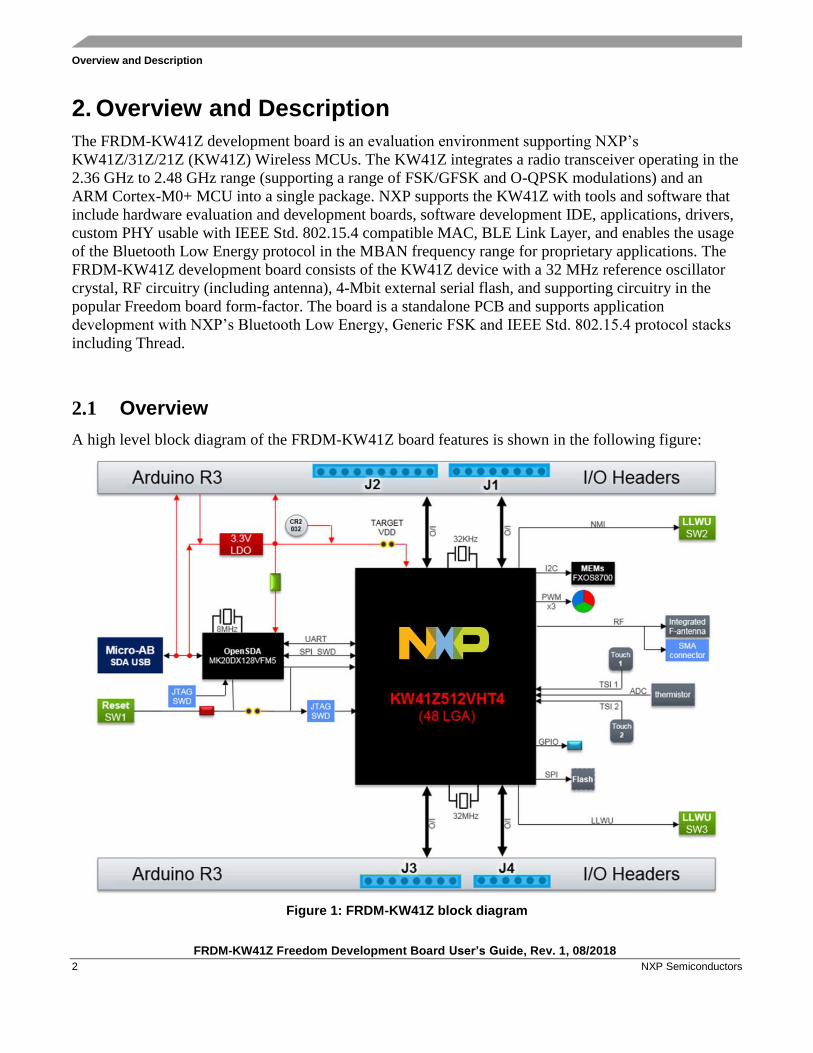
The following figure shows the main board features and Input/Output headers for the FRDM-KW41Z
board:
Figure 3: FRDM-KW41Z component placement.

Overview and Description
FRDM-KW41Z Freedom Development Board User’s Guide, Rev. 1, 08/2018
NXP Semiconductors 5
2.3 Serial and Debug Adapter
The FRDM-KW41Z development board includes OpenSDA v2.2-a serial and debug adapter circuit that
includes an open-source hardware design, an open-source bootloader, and debug interface software. It
bridges serial and debug communications between a USB host and an embedded target processor as
shown in Figure 4. The hardware circuit is based on a NXP Kinetis K20 family microcontroller (MCU)
with 128 KB of embedded flash and an integrated USB controller. OpenSDAv2.2 comes preloaded with
the DAPLink bootloader - an open-source mass storage device (MSD) bootloader and the Segger J-Link
Interface firmware, which provides a MSD flash programming interface, a virtual serial port interface,
and a J-Link debug interface. For more information on the OpenSDAv2.2 software, see mbed.org,
https://github.com/mbedmicro/DAPLink, and www.nxp.com/opensda.
Figure 4: OpenSDAv3.0 high-level block diagram.
OpenSDAv2.2 is managed by a Kinetis K20 MCU built on the ARM Cortex-M4 core. The
OpenSDAv2.2 circuit includes a status LED (D2) and a pushbutton (SW1). The pushbutton asserts the
Reset signal to the KW41Z target MCU. It can also be used to place the OpenSDAv2.2 circuit into
bootloader mode. UART and GPIO signals provide an interface to either the SWD debug port or the
K20. The OpenSDAv2.2 circuit receives power when the USB connector, J6, is plugged into a USB
host.
2.3.1 Virtual serial port
A serial port connection is available between the OpenSDAv2.2 MCU and pins PTC6 and PTC7 of the
KW41Z.
NOTE
To enable the Virtual COM, Debug, and MSD features, Segger J-Link drivers must be
installed. Download the drivers at
https://www.segger.com/downloads/jlink.

Functional description
FRDM-KW41Z Freedom Development Board User’s Guide, Rev. 1, 08/2018
6 NXP Semiconductors
3. Functional description
The four-layer board provides the KW41Z with its required RF circuitry, 32 MHz reference oscillator
crystal, and power supply with a DC-DC converter including Bypass, Buck, and Boost modes. The
layout for this base-level functionality can be used as a reference layout for your target board
3.1 RF circuit
The FRDM-KW41Z RF circuit provides an RF interface for users to begin application development. A
minimum matching network to the MCU antenna pin is provided through C4 and L1. An additional
matching component, L7, is provided to match the printed F-antenna to 50 ohm controlled line.
An optional SMA is located at J5. This is enabled by rotating the 10 pF capacitor in C8 to the location of
C7. The following figure shows the RF circuit in detail.
Figure 5: FRDM-KW41Z RF circuit.
3.2 Clocks
The FRDM-KW41Z board provides two clocks. A 32 MHz clock for clocking MCU and Radio, and a
32.768 kHz clock to provide an accurate low power time base:

Functional description
FRDM-KW41Z Freedom Development Board User’s Guide, Rev. 1, 08/2018
NXP Semiconductors 7
Figure 6: FRDM-KW41Z 32 MHz reference oscillator circuit.
• 32 MHz Reference Oscillator
o Figure 6 shows the 32 MHz external crystal Y1. The IEEE Std. 802.15.4 requires the
frequency to be accurate to less than 40 ppm
o Internal load capacitors provide the bulk of the crystal load capacitance.
o To measure the 32 MHz oscillator frequency, program the CLKOUT (PTB0) signal to
provide buffered output clock signal
Figure 7: FRDM-KW41Z 32.786 kHz oscillator circuit.
• 32.768 kHz Crystal Oscillator (for accurate low-power time base)
o A secondary 32.768 kHz crystal Y2 is provided (see Figure 9)
o Internal load capacitors provide the entire crystal load capacitance
o Zero ohm resistors are supplied to bypass the Y2 crystal
▪ This provides two extra GPIO to the I/O headers; PTB16 & PTB17
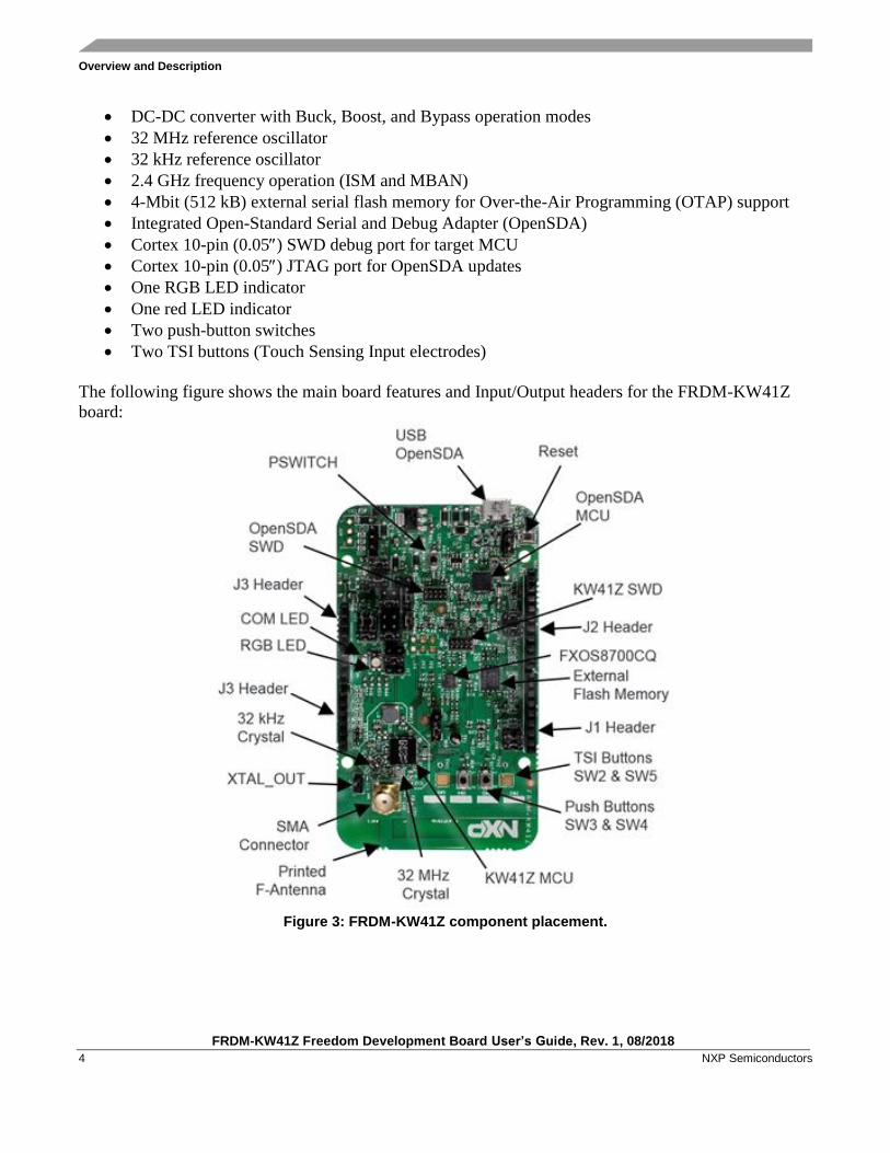
3.3 Power management
There are several different ways to power and measure current on the FRDM-KW41Z board. The
FRDM-KW41Z power-management circuit is shown in the following figure:
Functional description
FRDM-KW41Z Freedom Development Board User’s Guide, Rev. 1, 08/2018
8 NXP Semiconductors
Figure 8: FRDM-KW41Z power management circuit.
The FRDM-KW41Z can be powered by the following means:
• Through the micro USB type B connector (J6), which provides 5V to the P5V_USB signal into
the 3V3 LDO (U17)
• Through the Freedom development board headers, which provide either P3.3V or P5-9V_VIN on
header J3 pin-8 to LDO 3V3 (U17)
• From an external battery (Coin-cell – BT500)
• From an external DC supply in the following ways:
o Connect an adapter that can supply 1.8 to 3.6 VDC to J19 pins using the selector J23 pin
2-3
o Connect an unregulated external supply (of up to 5.5 VDC) to J19 pin 1 and the GND pin
to use the on board 3.3 V LDO regulator (using the selector J23 pin 1-2)
The 2-pin 12 headers J8 and J20 can supply current to various board components and can be used to
measure the current (if desired). Green LED marked as LED2 is available as a power indicator.
Power headers can supply either the LED, MCU, or peripheral circuits. Measure the current by inserting
a current meter in place of a designated jumper. See Table 4 in section 4.2 for details on jumper
descriptions.
The FRDM-KW41Z can be configured to use any of the DCDC converter operating modes. These
modes are Bypass, Buck (Manual-Start), Buck (Auto-Start), and Boost. Figure 9, Figure 10, Figure 11,
Figure 12, and Table 1 highlight the jumper settings for each of these modes.

Functional description
FRDM-KW41Z Freedom Development Board User’s Guide, Rev. 1, 08/2018
NXP Semiconductors 9
Figure 9: Jumper settings for Bypass mode.
Figure 10: Jumper settings for Boost mode.
Figure 11: Jumper settings for Buck mode (Manual-start).
Figure 12: Jumper settings for Buck mode (Auto-start).

Functional description
FRDM-KW41Z Freedom Development Board User’s Guide, Rev. 1, 08/2018
10 NXP Semiconductors
Table 1: DCDC configurations.
Mode J18 J16 J17 J22
Bypass Mode 1-2 1-2 3-4 1-3
2-4
5-6
Boost Mode 2-4 3-4 1-2
5-6
5-6
Buck Mode (manual
start)
2-4 5-6 3-4 5-6
Buck Mode (auto start) 2-4 3-4 3-4 5-6
3.4 Serial flash memory (SPI interface)
Component U4 is the AT45DB041E 4-Mbit (512 KB) serial flash memory with SPI interface. It is
intended for Over-the-Air Programming (OTAP) or for storing the non-volatile system data, or
parameters.
The figure below shows the memory circuit:
• Memory power supply is P3V3_BRD
• Discrete pull-up resistors pads for SPI port
• You can share the SPI with other peripherals using the J1 I/O header
• The SPI Write Protect and Reset have a discrete pull-up resistor
Figure 13: AT45DB041E 4-Mbit (512 KB) serial flash memory circuit.
Functional description
FRDM-KW41Z Freedom Development Board User’s Guide, Rev. 1, 08/2018
NXP Semiconductors 11
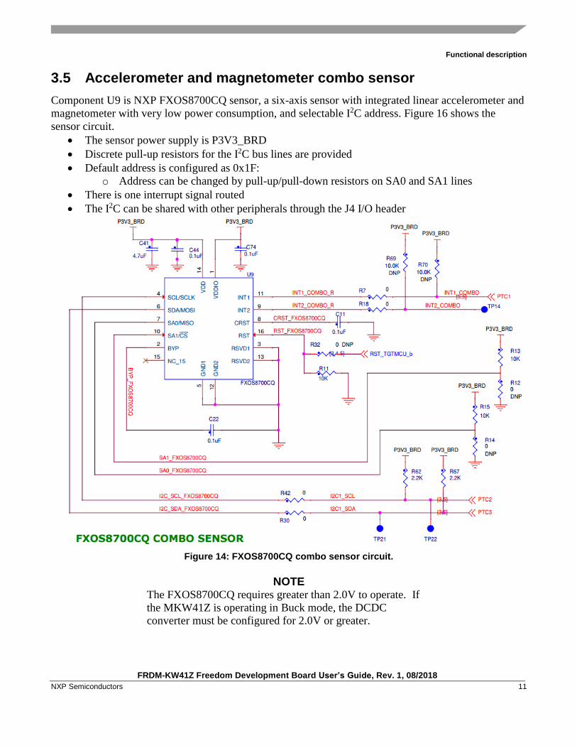
3.5 Accelerometer and magnetometer combo sensor
Component U9 is NXP FXOS8700CQ sensor, a six-axis sensor with integrated linear accelerometer and
magnetometer with very low power consumption, and selectable I2C address. Figure 16 shows the
sensor circuit.
• The sensor power supply is P3V3_BRD
• Discrete pull-up resistors for the I2C bus lines are provided
• Default address is configured as 0x1F:
o Address can be changed by pull-up/pull-down resistors on SA0 and SA1 lines
• There is one interrupt signal routed
• The I2C can be shared with other peripherals through the J4 I/O header
Figure 14: FXOS8700CQ combo sensor circuit.
NOTE
The FXOS8700CQ requires greater than 2.0V to operate. If
the MKW41Z is operating in Buck mode, the DCDC
converter must be configured for 2.0V or greater.
Functional description
FRDM-KW41Z Freedom Development Board User’s Guide, Rev. 1, 08/2018
12 NXP Semiconductors
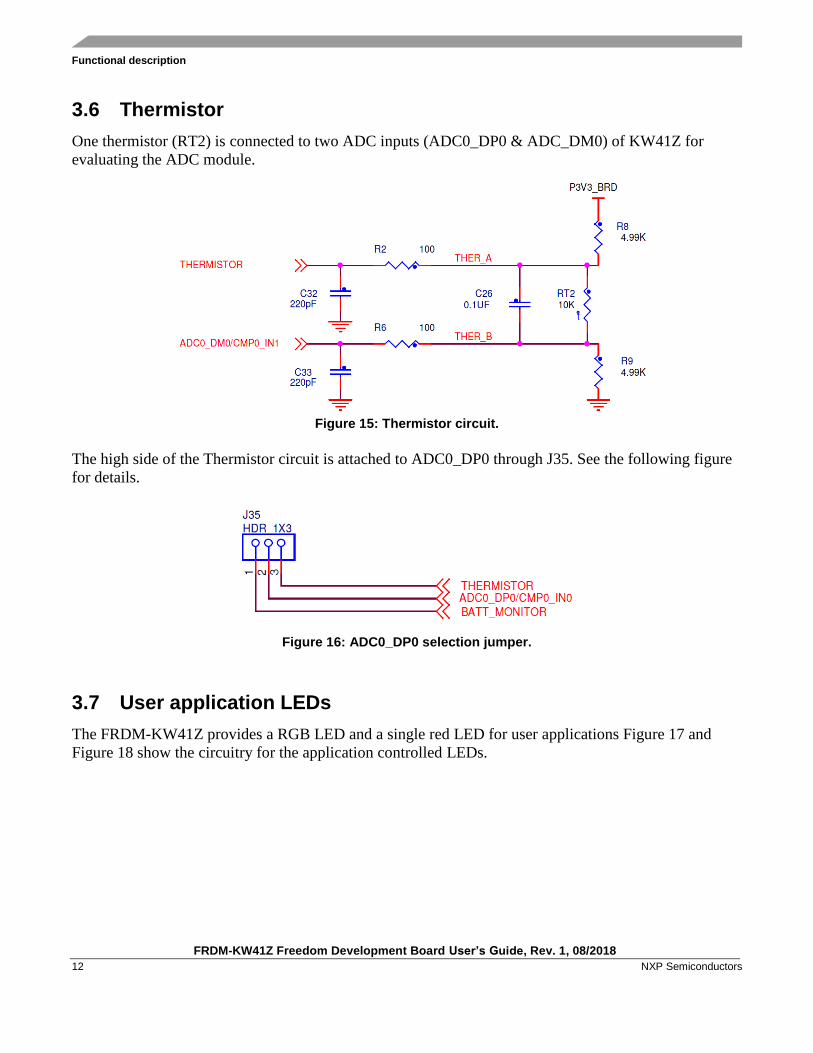
3.6 Thermistor
One thermistor (RT2) is connected to two ADC inputs (ADC0_DP0 & ADC_DM0) of KW41Z for
evaluating the ADC module.
Figure 15: Thermistor circuit.
The high side of the Thermistor circuit is attached to ADC0_DP0 through J35. See the following figure
for details.
Figure 16: ADC0_DP0 selection jumper.
3.7 User application LEDs
The FRDM-KW41Z provides a RGB LED and a single red LED for user applications Figure 17 and
Figure 18 show the circuitry for the application controlled LEDs.

Functional description
FRDM-KW41Z Freedom Development Board User’s Guide, Rev. 1, 08/2018
NXP Semiconductors 13
Figure 17. FRDM-KW41Z RGB LED circuit
Figure 18. FRDM-KW41Z LED3 circuit
NOTE
When operating in default Buck and Boost configurations, the
P3V3_LED supply will be at 1.8V. The Blue and Green LED in the
RGB LED will not illuminate at these voltages. To see these LEDs
illuminate in Buck and Boost modes, the application software must
increase the output voltage of the DCDC to 3V.

Functional description
FRDM-KW41Z Freedom Development Board User’s Guide, Rev. 1, 08/2018
14 NXP Semiconductors
3.8 Buttons and electrodes
Two tactile buttons and two TSI electrodes are populated on the FRDM-KW41Z for Human Machine
Interaction (HMI). The following figure shows the circuit for both the TSI electrodes and the tactile
buttons.
Figure 19.FRDM-KW41Z HMI circuit
3.9 IR transmitter
An optional infrared transmitter or blaster is provided to communicate over infra-red via the CMT
module on KW41Z.
Figure 19 shows the IR circuit.
• The IR power supply is P3V3_LED
• The IR has a range of approximately 10 meters
• The current draw is approximately 100 mA when active

Functional description
FRDM-KW41Z Freedom Development Board User’s Guide, Rev. 1, 08/2018
NXP Semiconductors 15
Figure 20. IR transmitter circuit.
NOTE
Components D11 and Q2 are not populated by default. These
must be populated for the IR transmitter circuit to function.
Headers and Jumpers
FRDM-KW41Z Freedom Development Board User’s Guide, Rev. 1, 08/2018
16 NXP Semiconductors
4. Headers and Jumpers
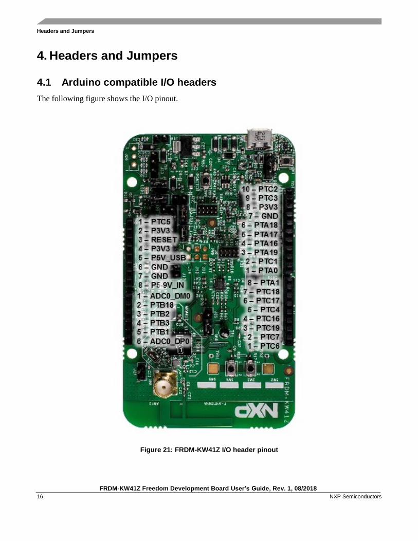
4.1 Arduino compatible I/O headers
The following figure shows the I/O pinout.
Figure 21: FRDM-KW41Z I/O header pinout

Headers and Jumpers
FRDM-KW41Z Freedom Development Board User’s Guide, Rev. 1, 08/2018
NXP Semiconductors 17
The following table shows the signals that can be multiplexed to each pin:
Table 2: Arduino compatible header/connector pinout (J1 and J2)
HDR Pin 1x10 Connector (J2) - Description IC
Pin 1 PTA0/TSI0_CH8/SPI0_PCS1/TPM1_CH0/DTEST12/SWD_DIO 1
2 PTC1/ANT_B/I2C0_SDA/UART0_RTS_b/TPM0_CH2/DTEST5/RF_ACTIVE 37
3 PTA19/TSI0_CH13/ADC0_SE5/LLWU_P7/SPI1_PSC0/TMP2_CH1/DTEST7/dcdc_testo5 7
4 PTA16/TSI0_CH10/LLWU_P4/SPI1_SOUT/TPM0_CH0/DTEST4/dcdc_testo2 4
5 PTA17/TSI0_CH11LLWU_P5/RF_RESET/SPI1_SIN/TPM_CLKIN1/DTEST5/dcdc_testo3 5
6 PTA18/TSI0_CH12/LLWU_P6/SPI1_SCK/TPM_CH0/DTEST6/dcdc_testo4 6
7 GND
8 VREFH/VREF_OUT 27
9 PTC3/TSI0_CH15/DIAG2/LLWU_P11/RX_SWITCH/I2C1_SDA/UART0_TX/TPM0_CH1/DTEST7/DTM_TX 39
10 PTC2/TSI0_CH14/DIAG1/LLWU_P10/TX_SWITCH/I2C1_SCL/UART0_RX/CMT_IRO/DTEST6/DTM_RX 38
HDR Pin 1x8 Connector (J1) - Description IC
Pin 1 PTC6/TSI0_CH2/LLWU_14/XTAL_OUT_EN/I2C1_SCL/UART0_RX/TPM2_CH0/DTEST2/BSM_FRAME 42
2 PTC7/TSI0_CH3/LLWU_P15/SPI0_PCS2/I2C1_SDA/UART0_TX/TPM2_CH1/DTEST3/BSM_DATA 43
3 PTC19/TSI0_CH7/LLWU_P3/SPI0_PCS0/I2C0_SCL/UART0_CTS_b/BSM_CLK/DTEST3/RF_ACTIVE 48
4 PTC16/TSI0_CH4/LLWU_P0/SPI0_SCK/I2C0_SDA/UART0_RTS_b/TPM0_CH3/DTEST0/dcdc_testo1 45
5 PTC4/TSI0_CH0/DIAG3/LLWU_P12/ANT_A/EXTRG_IN/UART0_CTS_b/TPM1_CH0/DTEST0/BSM_DATA 40
6A PTC17/TSI0_CH5/LLWU_P1/SPI0_SOUT/I2C1_SCL/UART0_RX/BSM_FRAME/DTEST1/DTM_RX 46
6B PTB16/EXTAL32K/I2C1_SCL/TPM2_CH0/DTEST10 21
7A PTC18/TSI0_CH6/LLWU_P2/SPI0_IN/I2C1_SDA/UART0_TX/BSM_DATA/DTEST2/DTM_TX 47
7B PTB17/XTAL32K/I2C1_SDA/TPM2_CH1/DTEST11/BSM_CLK 22
8 PTA1/TSI0_CH9/SPI1_PSC0/TPM1_CH1/DTEST13/SWD_CLK 2
Table 3: Arduino compatible header/connector pinout (J3 and J4)
HDR Pin 1x8 Connector (J3) - Description IC Pin
1 PTC5/TSI0_CH1/DIAG4/LLWU_P13/RF_OFF/LPTMR0_ALT2/UART0_RTS_b/TPM1_CH1/DTEST1/BSM_CLK
41
2 IOREF(3V3) -
3 PTA2/TPM0_CH3/RESET_b 3
4 3V3 -
5 5V -
6 GND -
7 GND -
8 5-9V IN -
HDR Pin 1x6 Connector (J4) - Description IC Pin
1 ADC0_DM0/CMP0_IN1 25
2 DAC0_OUT/ADC0_SE4/CMP0_IN2 23
3 ADC0_SE3/CMP0_IN3 18
4 ADC0_SE2/CMP0_IN4 19
5 ADC0_SE1/CMP0_IN5 17
6A ADC0_DP0/CMP0_IN0 24
6B PTB0/LLWU_P8/XTAL_OUT_EN/I2C0_SCL/CMP0_OUT/TPM0_CH1/DTEST11/CLKOUT 16

Headers and Jumpers
FRDM-KW41Z Freedom Development Board User’s Guide, Rev. 1, 08/2018
18 NXP Semiconductors
4.2 Jumper Table
The jumper settings on the FRDM-KW41Z are described in the following table. * denote jumper
selection is shorted on board by default. Bold text indicates default selection.
Table 4: FRDM-KW41Z jumper table
Jumper Option Setting Description
J8 P3V3_BRD 1-2 Isolate board supply to board peripherals
J12 SWD_CLK_TGTMCU 1-2* Isolate SWD_CLK from SWD header
J13 SWD_DIO 1-2* OpenSDA SWD_DIO isolation jumper
J14 SWD_CLK 1-2* OpenSDA SWD_CLK isolation jumper
J16 PSW_CFG 1-2
3-4
5-6
PSWITCH to ground
PSWITCH to VDCDC_IN
PSWITCH to SW6
J17 DCDC_CFG 3-4
1-2; 5-6
DCDC_CFG to VDCDC_IN
DCDC_CFG to ground; DCDC_LP to VDCDC__IN
J18 PWR_CFG 1-2
2-4
V_BATT to P3V3
VDD_1P8F to P3V3
J20 P3V3_LED_PWR 1-2 Isolate board power LED supply
J22 REG_CFG 1-3; 2-4; 5-6
5-6
V_MCU to VDD_1P8F; V_MCU to 1.5V; DCDC VDD_1P8 to VDD_1P8F
VDD_1P8 to VDD_1P8F
J23 V_EXT_CON 1-2
2-3
Connect external supply to VIN of U17 (regulator)
Connect external supply to V_BATT
J24 RST Button Bypass 1-2
2-3
Reset button connected to OpenSDA
Reset button connected to Target MCU
J25 SDA_RST_TGTMCU 1-2* Isolate OpenSDA MCU from target MCU reset signal
J27 V_BATT 1-2 Isolate battery from V_BATT
J28/J29 SPI IN/OUT J28-1 J28-22 /
J29-1 J29-2
J28-1 J29-2 /
J28-2 J29-1
SOUT to J2-4 / SIN to J2-5
SOUT to J2-5 / SIN to J2-4
J30/J31 UART RX/TX J30-1 J30-2 /
J31-1 J31-2
J30-1 J31-2 /
J30-2 J31-1
RX to J1-1 / TX to J1-2
RX to J1-2 / TX to J1-1
J33 V_LDO 1-2 Isolate V_BATT from 3.3V regulator (V_LDO)
J34 V_BATT_VDCDC_IN 1-2 Isolate VDCDC_IN from V_BATT
J35 ADC SELECTOR 2-3
1-2
ADC0_DP0 to THERMISTOR
ACD0_DP0 to BATT_MONITOR

Revision history
FRDM-KW41Z Freedom Development Board User’s Guide, Rev. 1, 08/2018
NXP Semiconductors 19
5. References
The following references are available on www.nxp.com/FRDM-KW41Z:
• FRDM-KW41Z Design Package
6. Revision history
Table 5. Revision history
Rev. Date Substantive change(s) 0 10/2016 Initial release
1 08/2018 Updated OpenSDA chapter; Corrected
Figure 5; Added operation note for
FXOS8700 sensor.

Document Number: FRDMKW41ZUG Rev. 1
08/2018
How to Reach Us:
Home Page:
nxp.com
Web Support:
nxp.com/support
Information in this document is provided solely to enable system and software implementers to
use NXP products. There are no express or implied copyright licenses granted hereunder to
design or fabricate any integrated circuits based on the information in this document. NXP
reserves the right to make changes without further notice to any products herein.
NXP makes no warranty, representation, or guarantee regarding the suitability of its products for
any particular purpose, nor does NXP assume any liability arising out of the application or use of
any product or circuit, and specifically disclaims any and all liability, including without limitation
consequential or incidental damages. “Typical” parameters that may be provided in NXP data
sheets and/or specifications can and do vary in different applications, and actual performance
may vary over time. All operating parameters, including “typicals,” must be validated for each
customer application by customer's technical experts. NXP does not convey any license under its
patent rights nor the rights of others. NXP sells products pursuant to standard terms and
conditions of sale, which can be found at the following address:
nxp.com/SalesTermsandConditions.
While NXP has implemented advanced security features, all products may be subject to
unidentified vulnerabilities. Customers are responsible for the design and operation of their
applications and products to reduce the effect of these vulnerabilities on customer’s applications
and products, and NXP accepts no liability for any vulnerability that is discovered. Customers
should implement appropriate design and operating safeguards to minimize the risks associated
with their applications and products.
NXP, the NXP logo, NXP SECURE CONNECTIONS FOR A SMARTER WORLD, COOLFLUX,
EMBRACE, GREENCHIP, HITAG, I2C BUS, ICODE, JCOP, LIFE VIBES, MIFARE, MIFARE
CLASSIC, MIFARE DESFire, MIFARE PLUS, MIFARE FLEX, MANTIS, MIFARE ULTRALIGHT,
MIFARE4MOBILE, MIGLO, NTAG, ROADLINK, SMARTLX, SMARTMX, STARPLUG, TOPFET,
TRENCHMOS, UCODE, Freescale, the Freescale logo, AltiVec, C 5, CodeTEST, CodeWarrior,
ColdFire, ColdFire+, C Ware, the Energy Efficient Solutions logo, Kinetis, Layerscape, MagniV,
mobileGT, PEG, PowerQUICC, Processor Expert, QorIQ, QorIQ Qonverge, Ready Play,
SafeAssure, the SafeAssure logo, StarCore, Symphony, VortiQa, Vybrid, Airfast, BeeKit,
BeeStack, CoreNet, Flexis, MXC, Platform in a Package, QUICC Engine, SMARTMOS, Tower,
TurboLink, and UMEMS are trademarks of NXP B.V. All other product or service names are the
property of their respective owners., Cortex, Jazelle, Keil, SecurCore, Thumb, TrustZone, and
μVision are registered trademarks of Arm Limited (or its subsidiaries) in the EU and/or
elsewhere. Arm7, Arm9, Arm11, big.LITTLE, CoreLink, CoreSight, DesignStart, Mali, Mbed,
NEON, POP, Sensinode, Socrates, ULINK and Versatile are trademarks of Arm Limited (or its
subsidiaries) in the EU and/or elsewhere. All rights reserved. Oracle and Java are registered
trademarks of Oracle and/or its affiliates. The Power Architecture and Power.org word marks and
the Power and Power.org logos and related marks are trademarks and service marks licensed by
Power.org.
© 2016- 2018 NXP B.V.