Embed Size (px)
Citation preview
© 2016 NXP B.V.
FRDM-K64F Freedom Module User’s Guide
1. Introduction
The NXP Freedom development platform is a set of
software and hardware tools for evaluation and
development. It is ideal for rapid prototyping of
microcontroller-based applications. The NXP Freedom
K64 hardware, FRDM-K64F, is a simple, yet
sophisticated design featuring a Kinetis K series
microcontroller, built on the ARM®
Cortex®-M4 core.
FRDM-K64F can be used to evaluate the K64, K63, and
K24 Kinetis K series devices. It features the
MK64FN1M0VLL12 MCU, which boast the maximum
operation frequency of 120 MHz, 1 MB of flash, 256
KB RAM, a full-speed USB controller, Ethernet
controller, secure digital host controller, and analog and
digital peripherals. The FRDM-K64F hardware is form-
factor compatible with the ArduinoTM
R3 pin layout,
providing a broad range of expansion board options.
The onboard interface includes a six-axis digital
accelerometer & magnetometer, RGB LED, SDHC,
add-on Bluetooth module, add-on RF module, and
Ethernet.
The FRDM-K64F platform features OpenSDAv2, the
NXP open-source hardware embedded serial and debug
adapter running an open-source bootloader. This circuit
offers several options for serial communication, flash
programming, and run-control debugging. OpenSDAv2
is an mbed™ HDK-compatible debug interface
preloaded with the open-source CMSIS-DAP Interface
firmware (mbed interface) for rapid prototyping and
product development, with a focus on connected
Internet of Things devices.
NXP Semiconductors Document Number: FRDMK64FUG
User's Guide Rev. 1 , 08/2016
Contents
1. Introduction ........................................................................ 1 2. FRDM-K64F Hardware Overview ..................................... 2 3. FRDM-K64F Hardware Description .................................. 4
3.1. Power supply .......................................................... 4 3.2. Serial and Debug Adapter version 2 (OpenSDAv2) 6
4. Microcontroller .................................................................. 7 5. Clocking ............................................................................. 9 6. USB ................................................................................. 10 7. Secure Digital Card .......................................................... 11 8. Ethernet ............................................................................ 12 9. Accelerometer and Magnetometer .................................... 13 10. RGB LED ........................................................................ 13 11. Serial Port ........................................................................ 14 12. Reset ................................................................................ 14 13. Push Button Switches....................................................... 15 14. Debug ............................................................................... 15 15. Add-on modules ............................................................... 15
15.1. RF module ............................................................ 15 15.2. Bluetooth module .................................................. 16
16. Input/output connectors .................................................... 16 17. Arduino Compatibility ..................................................... 18 18. References ........................................................................ 18 19. Revision History .............................................................. 18
FRDM-K64F Hardware Overview
FRDM-K64F Freedom Module User’s Guide, User's Guide, Rev. 1, 08/2016
2 NXP Semiconductors
2. FRDM-K64F Hardware Overview
The features of the FRDM-K64F hardware are as follows:
• MK64FN1M0VLL12 MCU (120 MHz, 1 MB flash memory, 256 KB RAM, low-power, crystal-
less USB, and 100 LQFP)
• Dual role USB interface with micro-B USB connector
• RGB LED
• FXOS8700CQ – accelerometer and magnetometer
• Two user push buttons
• Flexible power supply option – OpenSDAv2 USB, K64 USB, and external source
• Easy access to MCU input/output through Arduino R3TM
compatible I/O connectors
• Programmable OpenSDAv2 debug circuit supporting the CMSIS-DAP Interface software that
provides:
— Mass storage device (MSD) flash programming interface
— CMSIS-DAP debug interface over a driver-less USB HID connection providing run-
control debugging and compatibility with IDE tools
— Virtual serial port interface
— Open-source CMSIS-DAP software project: github.com/mbedmicro/CMSIS-DAP
• Ethernet
• SDHC
• Add-on RF module: nRF24L01+ Nordic 2.4GHz Radio
• Add-on Bluetooth module: JY-MCU BT board V1.05 BT
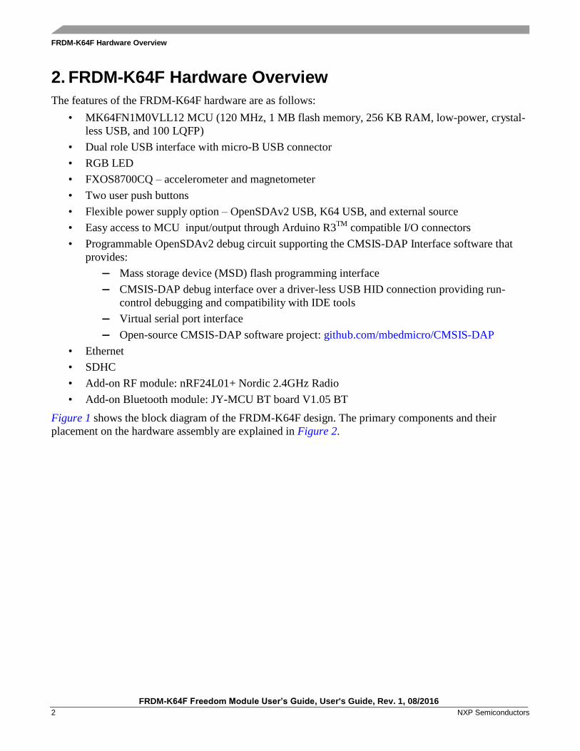
Figure 1 shows the block diagram of the FRDM-K64F design. The primary components and their
placement on the hardware assembly are explained in Figure 2.
FRDM-K64F Hardware Overview
FRDM-K64F Freedom Module User’s Guide, User's Guide, Rev. 1, 08/2016
NXP Semiconductors 3
Figure 1. FRDM-K64F block diagram
FRDM-K64F Hardware Description
FRDM-K64F Freedom Module User’s Guide, User's Guide, Rev. 1, 08/2016
4 NXP Semiconductors
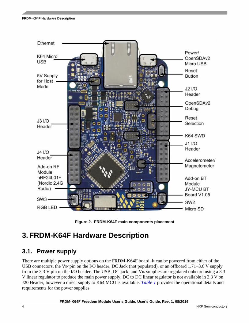
Figure 2. FRDM-K64F main components placement
3. FRDM-K64F Hardware Description
3.1. Power supply
There are multiple power supply options on the FRDM-K64F board. It can be powered from either of the
USB connectors, the VIN pin on the I/O header, DC Jack (not populated), or an offboard 1.71–3.6 V supply
from the 3.3 V pin on the I/O header. The USB, DC jack, and VIN supplies are regulated onboard using a 3.3
V linear regulator to produce the main power supply. DC to DC linear regulator is not available in 3.3 V on
J20 Header, however a direct supply to K64 MCU is available. Table 1 provides the operational details and
requirements for the power supplies.

FRDM-K64F Hardware Description
FRDM-K64F Freedom Module User’s Guide, User's Guide, Rev. 1, 08/2016
NXP Semiconductors 5
Table 1. FRDM-K64F power requirements
Supply source Valid range OpenSDAv2 operational? Regulated onboard?
OpenSDAv2 USB 5 V Yes Yes
K64 USB 5 V No Yes
VIN Pin 5-9 V No Yes
3.3V Header (J20) 1.71-3.6 V No No
DC Jack (Not Populated) 5-9 V No Yes
NOTE
The OpenSDAv2 circuit is only operational when a USB cable is
connected and supplying power to OpenSDAv2 USB. However, the
protection circuitry is in place to enable multiple sources to be powered at
once.
Figure 3. Power supply schematic
Table 2. FRDM-K64F power supplies
Power supply name Description
P5–9V_VIN Power supplied from the VIN pin of the I/O headers (J3 pin 16). A Schottky diode provides back
drive protection.
P5V_SDA_PSW Power supplied from the OpenSDAv2 USB connector. A Schottky diode provides back drive
protection.
P5V_K64_USB Power supplied from the K64 USB connector. A Schottky diode provides back drive protection.
DC_JACK Power supplied from the DC Jack (not populated) connector. A Schottky diode provides back drive
protection.
P3V3_VREG Regulated 3.3V supply. Sources power to the P3V3 supply rail through a back drive protection
Schottky diode1.
P3V3_K64 K64 MCU supply. Header J20 provides a convenient means for energy consumption
measurements2.
P3V3_SDA OpenSDAv2 circuit supply. Header J18 provides a convenient means for energy consumption
measurements.
P5V_USB Nominal 5 V supplied to the I/O headers (J3 pin 10).
1. By default, the linear regulator, U17, is a 3.3 V output regulator. This is a common footprint that would allow the user to modify the assembly to utilize an alternative device, such as 1.8 V. The K64 microcontroller has an operating range of 1.71 V to 3.6 V.
2. By default, the J18 and J20 headers are populated. P3V3_K64 rail is connected with two resistors, R64 and R66. To measure the energy consumption of the K64 MCU, the trace between J20 pin 1 and 2 must be first cut. A current probe or shunt resistor and voltage meter can then be applied to measure the energy consumption on these rails.
FRDM-K64F Hardware Description
FRDM-K64F Freedom Module User’s Guide, User's Guide, Rev. 1, 08/2016
6 NXP Semiconductors
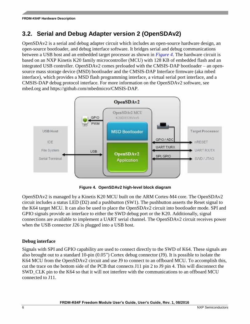
3.2. Serial and Debug Adapter version 2 (OpenSDAv2)
OpenSDAv2 is a serial and debug adapter circuit which includes an open-source hardware design, an
open-source bootloader, and debug interface software. It bridges serial and debug communications
between a USB host and an embedded target processor as shown in Figure 4. The hardware circuit is
based on an NXP Kinetis K20 family microcontroller (MCU) with 128 KB of embedded flash and an
integrated USB controller. OpenSDAv2 comes preloaded with the CMSIS-DAP bootloader – an open-
source mass storage device (MSD) bootloader and the CMSIS-DAP Interface firmware (aka mbed
interface), which provides a MSD flash programming interface, a virtual serial port interface, and a
CMSIS-DAP debug protocol interface. For more information on the OpenSDAv2 software, see
mbed.org and https://github.com/mbedmicro/CMSIS-DAP.
Figure 4. OpenSDAv2 high-level block diagram
OpenSDAv2 is managed by a Kinetis K20 MCU built on the ARM Cortex-M4 core. The OpenSDAv2
circuit includes a status LED (D2) and a pushbutton (SW1). The pushbutton asserts the Reset signal to
the K64 target MCU. It can also be used to place the OpenSDAv2 circuit into bootloader mode. SPI and
GPIO signals provide an interface to either the SWD debug port or the K20. Additionally, signal
connections are available to implement a UART serial channel. The OpenSDAv2 circuit receives power
when the USB connector J26 is plugged into a USB host.
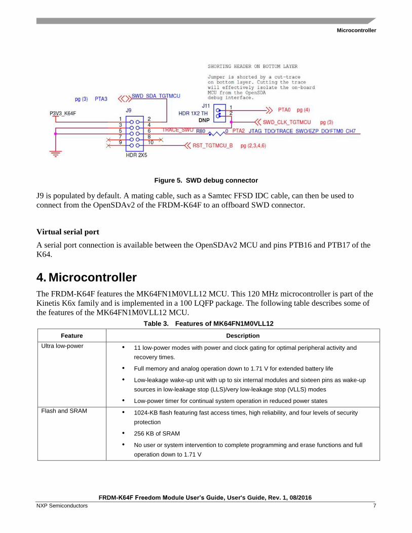
Debug interface
Signals with SPI and GPIO capability are used to connect directly to the SWD of K64. These signals are
also brought out to a standard 10-pin (0.05”) Cortex debug connector (J9). It is possible to isolate the
K64 MCU from the OpenSDAv2 circuit and use J9 to connect to an offboard MCU. To accomplish this,
cut the trace on the bottom side of the PCB that connects J11 pin 2 to J9 pin 4. This will disconnect the
SWD_CLK pin to the K64 so that it will not interfere with the communications to an offboard MCU
connected to J11.
Microcontroller
FRDM-K64F Freedom Module User’s Guide, User's Guide, Rev. 1, 08/2016
NXP Semiconductors 7
Figure 5. SWD debug connector
J9 is populated by default. A mating cable, such as a Samtec FFSD IDC cable, can then be used to
connect from the OpenSDAv2 of the FRDM-K64F to an offboard SWD connector.
Virtual serial port
A serial port connection is available between the OpenSDAv2 MCU and pins PTB16 and PTB17 of the
K64.
4. Microcontroller
The FRDM-K64F features the MK64FN1M0VLL12 MCU. This 120 MHz microcontroller is part of the
Kinetis K6x family and is implemented in a 100 LQFP package. The following table describes some of
the features of the MK64FN1M0VLL12 MCU.
Table 3. Features of MK64FN1M0VLL12
Feature Description
Ultra low-power • 11 low‐power modes with power and clock gating for optimal peripheral activity and
recovery times.
• Full memory and analog operation down to 1.71 V for extended battery life
• Low‐leakage wake‐up unit with up to six internal modules and sixteen pins as wake‐up
sources in low‐leakage stop (LLS)/very low‐leakage stop (VLLS) modes
• Low‐power timer for continual system operation in reduced power states
Flash and SRAM • 1024‐KB flash featuring fast access times, high reliability, and four levels of security
protection
• 256 KB of SRAM
• No user or system intervention to complete programming and erase functions and full
operation down to 1.71 V
Microcontroller
FRDM-K64F Freedom Module User’s Guide, User's Guide, Rev. 1, 08/2016
8 NXP Semiconductors
Table 3. Features of MK64FN1M0VLL12
Feature Description
Mixed‐signal capability • High‐speed 16‐bit ADC with configurable resolution
• Single or differential output modes for improved noise rejection
• 500 ns conversion time achievable with programmable delay block triggering
• Two high‐speed comparators providing fast and accurate motor overcurrent protection by
driving PWMs to a safe state
• Optional analog voltage reference provides an accurate reference to analog blocks
• One 12-bit DACs
Performance • 120 MHz ARM Cortex‐M4 core with DSP instruction set, single precision floating point
unit, single cycle MAC, and single instruction multiple data (SIMD) extensions
• Up to four channel DMA for peripheral and memory servicing with reduced CPU loading
and faster system throughput
• Cross bar switch enables concurrent multimaster bus accesses, increasing bus bandwidth
• Independent flash banks allowing concurrent code execution and firmware updating with
no performance degradation or complex coding routines
Timing and control • Four Flex Timers with a total of 20 channels
• Hardware dead‐time insertion and quadrature decoding for motor control
• Carrier modulator timer for infrared waveform generation in remote control applications
• Four‐channel 32‐bit periodic interrupt timer provides time base for RTOS task scheduler
or trigger source for ADC conversion and programmable delay block
• One low-power timer
• One independent real-time clock
Connectivity and communications
• Full‐Speed USB device/host/on‐the‐go with device charge detect capability
• Optimized charging current/time for portable USB devices, enabling longer battery life
• USB low‐voltage regulator supplies up to 120 mA off-chip at 3.3 volts to power external
components from 5‐volt input
• Five UARTs:
— One UART supports RS232 with flow control, RS485, and ISO7816
— Four UARTs support RS232 with flow control and RS485
• One Inter‐IC Sound (I2S) serial interface for audio system interfacing
• Three DSPI modules and three I2C modules
• Secured digital host controller (SDHC)
• One FlexCAN module
• One Ethernet module with 1588
• A multifunction external bus interface (FlexBUS) controller capable of interfacing to slave-
only devices.
Clocking
FRDM-K64F Freedom Module User’s Guide, User's Guide, Rev. 1, 08/2016
NXP Semiconductors 9
Table 3. Features of MK64FN1M0VLL12
Feature Description
Reliability, safety and
security • Hardware encryption coprocessor for secure data transfer and storage. Faster than
software implementations and with minimal CPU loading. Supports a wide variety of
algorithms ‐ DES, 3DES, AES, MD5, SHA‐1, SHA‐256
• Memory protection unit provides memory protection for all masters on the cross bar
switch, increasing software reliability
• Cyclic redundancy check (CRC) engine validates memory contents and communication
data, increasing system reliability
• Independently‐clocked COP guards against clock skew or code runaway for fail‐safe
applications, such as the IEC 60730 safety standard for household appliances
• External watchdog monitor drives output pin to safe state for external components in the
event that a watchdog timeout occurs
• Included in NXP product longevity program, with assured supply for a minimum of 10
years after launch
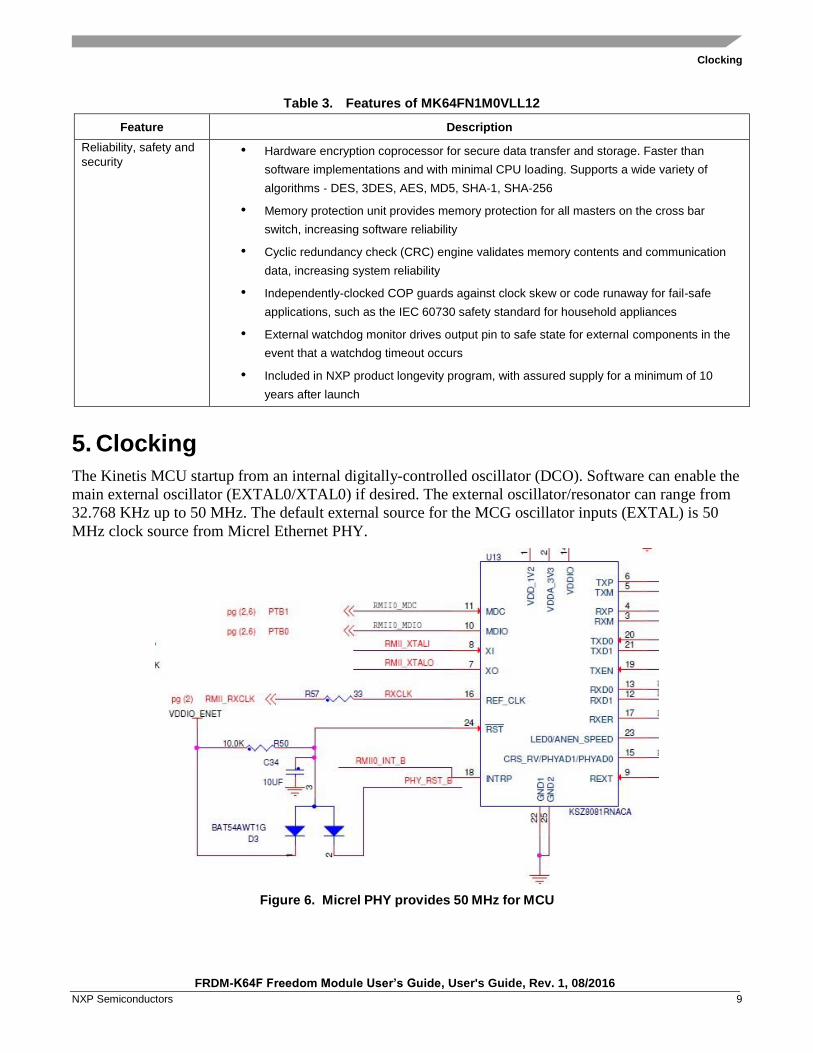
5. Clocking
The Kinetis MCU startup from an internal digitally-controlled oscillator (DCO). Software can enable the
main external oscillator (EXTAL0/XTAL0) if desired. The external oscillator/resonator can range from
32.768 KHz up to 50 MHz. The default external source for the MCG oscillator inputs (EXTAL) is 50
MHz clock source from Micrel Ethernet PHY.
Figure 6. Micrel PHY provides 50 MHz for MCU
USB
FRDM-K64F Freedom Module User’s Guide, User's Guide, Rev. 1, 08/2016
10 NXP Semiconductors
Figure 7. MCU receives RMII clock from Micrel Ethernet PHY
By default, the 32.768 KHz crystal is connected to the RTC oscillator inputs.
Figure 8. 32.768 KHz crystal for RTC
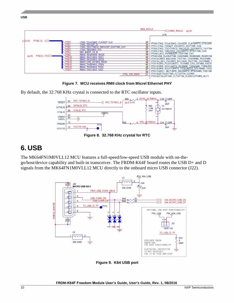
6. USB
The MK64FN1M0VLL12 MCU features a full-speed/low-speed USB module with on-the-
go/host/device capability and built-in transceiver. The FRDM-K64F board routes the USB D+ and D
signals from the MK64FN1M0VLL12 MCU directly to the onboard micro USB connector (J22).
Figure 9. K64 USB port
Secure Digital Card
FRDM-K64F Freedom Module User’s Guide, User's Guide, Rev. 1, 08/2016
NXP Semiconductors 11
When the FRDM-K64F board is operating in USB host mode, J21 must be shunt to supply 5 V power
from VBUS (J22). The source of 5 V power can be OpenSDAv2 USB port (J26), pin 10 of J3 I/O
header, and P5-9V_VIN DC-DC converter of J27.
Figure 10. K64 USB power input for host mode
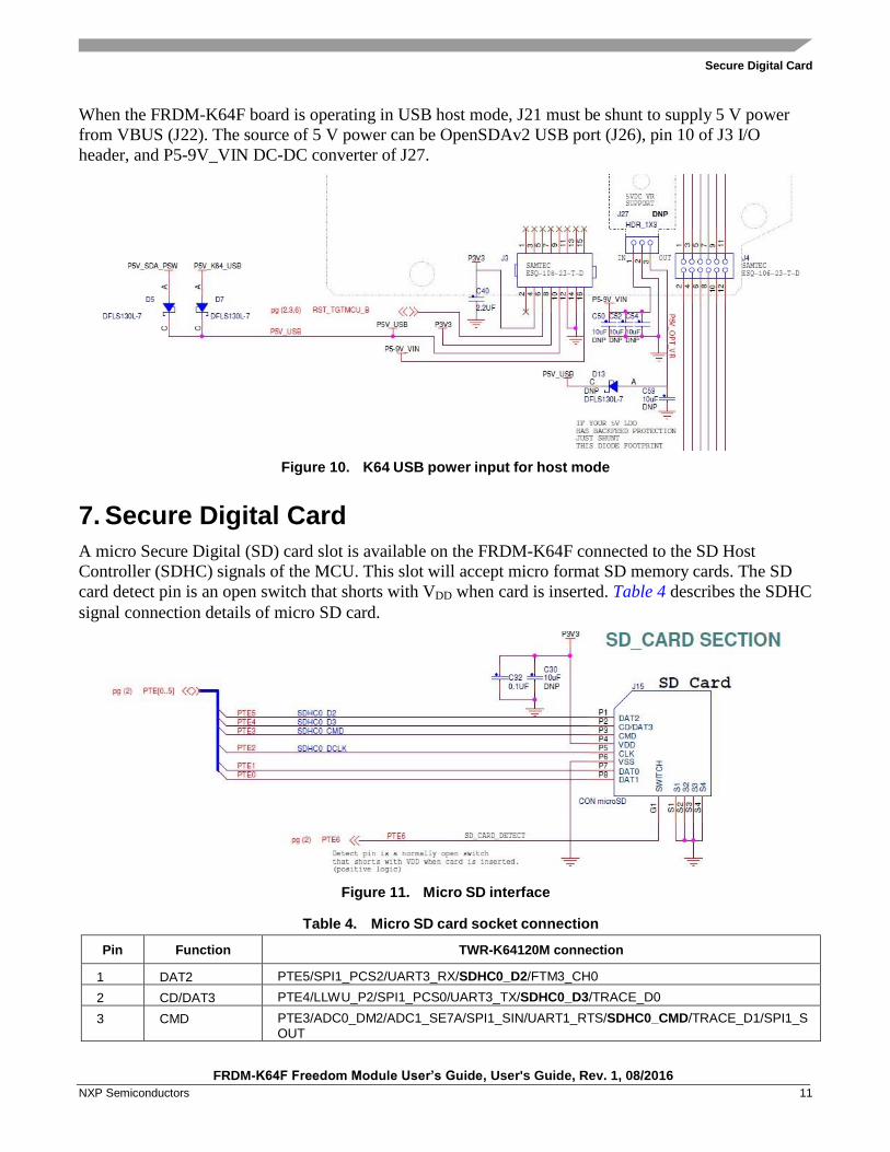
7. Secure Digital Card
A micro Secure Digital (SD) card slot is available on the FRDM-K64F connected to the SD Host
Controller (SDHC) signals of the MCU. This slot will accept micro format SD memory cards. The SD
card detect pin is an open switch that shorts with VDD when card is inserted. Table 4 describes the SDHC
signal connection details of micro SD card.
Figure 11. Micro SD interface
Table 4. Micro SD card socket connection
Pin Function TWR-K64120M connection
1 DAT2 PTE5/SPI1_PCS2/UART3_RX/SDHC0_D2/FTM3_CH0
2 CD/DAT3 PTE4/LLWU_P2/SPI1_PCS0/UART3_TX/SDHC0_D3/TRACE_D0
3 CMD PTE3/ADC0_DM2/ADC1_SE7A/SPI1_SIN/UART1_RTS/SDHC0_CMD/TRACE_D1/SPI1_S
OUT
Ethernet
FRDM-K64F Freedom Module User’s Guide, User's Guide, Rev. 1, 08/2016
12 NXP Semiconductors
Table 4. Micro SD card socket connection
Pin Function TWR-K64120M connection
4 VDD 3.3 V board supply (V_BRD)
5 CLK PTE2/LLWU_P1/ADC0_DP2/ADC1_SE6A/SPI1_SCK/UART1_CTS/SDHC0_DCLK/TRACE
_D2
6 VSS Ground
7 DAT0 PTE1/LLWU_P0/ADC1_SE5A/SPI1_SOUT/UART1_RX/SDHC0_D0/TRACE_D3/I2C1_S
CL/SPI1_ SIN
8 DAT1 PTE0/ADC1_SE4A/SPI1_PCS1/UART1_TX/SDHC0_D1/TRACE_CLKOUT/I2C1_SDA/RT
C_CLKO UT
G1 SWITCH PTE6/SPI1_PCS3/UART3_CTS_b/I2S0_MCLK/FTM3_CH1/USB0_SOF_OUT
S1-S4 S1, S2, S3, S4 Shield ground
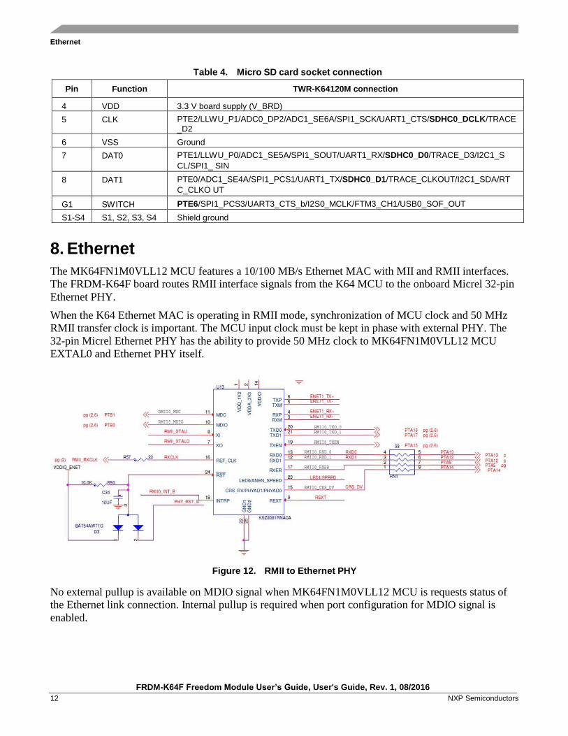
8. Ethernet
The MK64FN1M0VLL12 MCU features a 10/100 MB/s Ethernet MAC with MII and RMII interfaces.
The FRDM-K64F board routes RMII interface signals from the K64 MCU to the onboard Micrel 32-pin
Ethernet PHY.
When the K64 Ethernet MAC is operating in RMII mode, synchronization of MCU clock and 50 MHz
RMII transfer clock is important. The MCU input clock must be kept in phase with external PHY. The
32-pin Micrel Ethernet PHY has the ability to provide 50 MHz clock to MK64FN1M0VLL12 MCU
EXTAL0 and Ethernet PHY itself.
Figure 12. RMII to Ethernet PHY
No external pullup is available on MDIO signal when MK64FN1M0VLL12 MCU is requests status of
the Ethernet link connection. Internal pullup is required when port configuration for MDIO signal is
enabled.
RGB LED
FRDM-K64F Freedom Module User’s Guide, User's Guide, Rev. 1, 08/2016
NXP Semiconductors 13
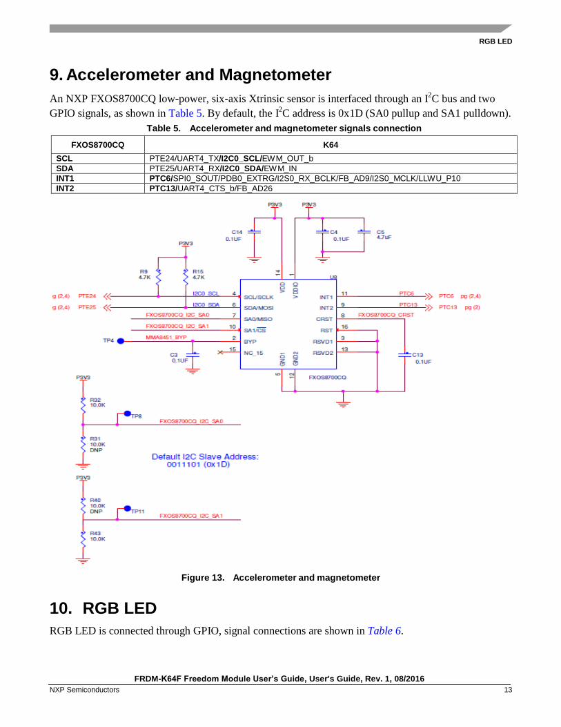
9. Accelerometer and Magnetometer
An NXP FXOS8700CQ low-power, six-axis Xtrinsic sensor is interfaced through an I2C bus and two
GPIO signals, as shown in Table 5. By default, the I2C address is 0x1D (SA0 pullup and SA1 pulldown).
Table 5. Accelerometer and magnetometer signals connection
FXOS8700CQ K64
SCL PTE24/UART4_TX/I2C0_SCL/EWM_OUT_b
SDA PTE25/UART4_RX/I2C0_SDA/EWM_IN
INT1 PTC6/SPI0_SOUT/PDB0_EXTRG/I2S0_RX_BCLK/FB_AD9/I2S0_MCLK/LLWU_P10
INT2 PTC13/UART4_CTS_b/FB_AD26
Figure 13. Accelerometer and magnetometer
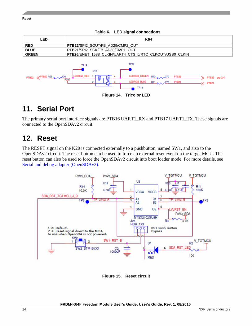
10. RGB LED
RGB LED is connected through GPIO, signal connections are shown in Table 6.
Reset
FRDM-K64F Freedom Module User’s Guide, User's Guide, Rev. 1, 08/2016
14 NXP Semiconductors
Table 6. LED signal connections
LED K64
RED PTB22/SPI2_SOUT/FB_AD29/CMP2_OUT
BLUE PTB21/SPI2_SCK/FB_AD30/CMP1_OUT
GREEN PTE26/ENET_1588_CLKIN/UART4_CTS_b/RTC_CLKOUT/USB0_CLKIN
Figure 14. Tricolor LED
11. Serial Port
The primary serial port interface signals are PTB16 UART1_RX and PTB17 UART1_TX. These signals are
connected to the OpenSDAv2 circuit.
12. Reset
The RESET signal on the K20 is connected externally to a pushbutton, named SW1, and also to the
OpenSDAv2 circuit. The reset button can be used to force an external reset event on the target MCU. The
reset button can also be used to force the OpenSDAv2 circuit into boot loader mode. For more details, see
Serial and debug adapter (OpenSDAv2).
Figure 15. Reset circuit
Add-on modules
FRDM-K64F Freedom Module User’s Guide, User's Guide, Rev. 1, 08/2016
NXP Semiconductors 15
13. Push Button Switches
Two push buttons, SW2 and SW3, are available on FRDM-K64F board, where SW2 is connected to
PTC6 and SW3 is connected to PTA4. Besides the general purpose input/output functions, SW2 and
SW3 can be low-power wake up signal. Also, only SW3 can be a non-maskable interrupt.
Table 7. Push button GPIO function
Switch GPIO Function
SW2 PTC6/SPI0_SOUT/PD0_EXTRG/I2S0_RX_BCLK/FB_AD9/I2S0_MCLK/LLWU_P10
SW3 PTA4/FTM0_CH1/NMI_b/LLWU_P3
14. Debug
The debug interface on MK64FN1M0VLL12 MCU is a Serial Wire Debug (SWD) port with trace output
capability. There are two debug interfaces on the FRDM-K64F: onboard OpenSDAv2 circuit (J26) and K64
direct SWD connection (J9).
NOTE
To use an external debugger, such as J-Link, you may need to disconnect
the OpenSDA SWD from the K64. To do this on the FRDM-K64F board,
cut the shorting trace which connects the pins of jumper holes on
connectors J8 and J12.
15. Add-on modules
15.1. RF module
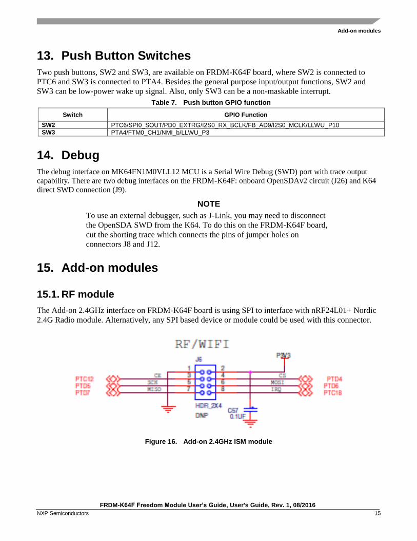
The Add-on 2.4GHz interface on FRDM-K64F board is using SPI to interface with nRF24L01+ Nordic
2.4G Radio module. Alternatively, any SPI based device or module could be used with this connector.
Figure 16. Add-on 2.4GHz ISM module
Input/output connectors
FRDM-K64F Freedom Module User’s Guide, User's Guide, Rev. 1, 08/2016
16 NXP Semiconductors
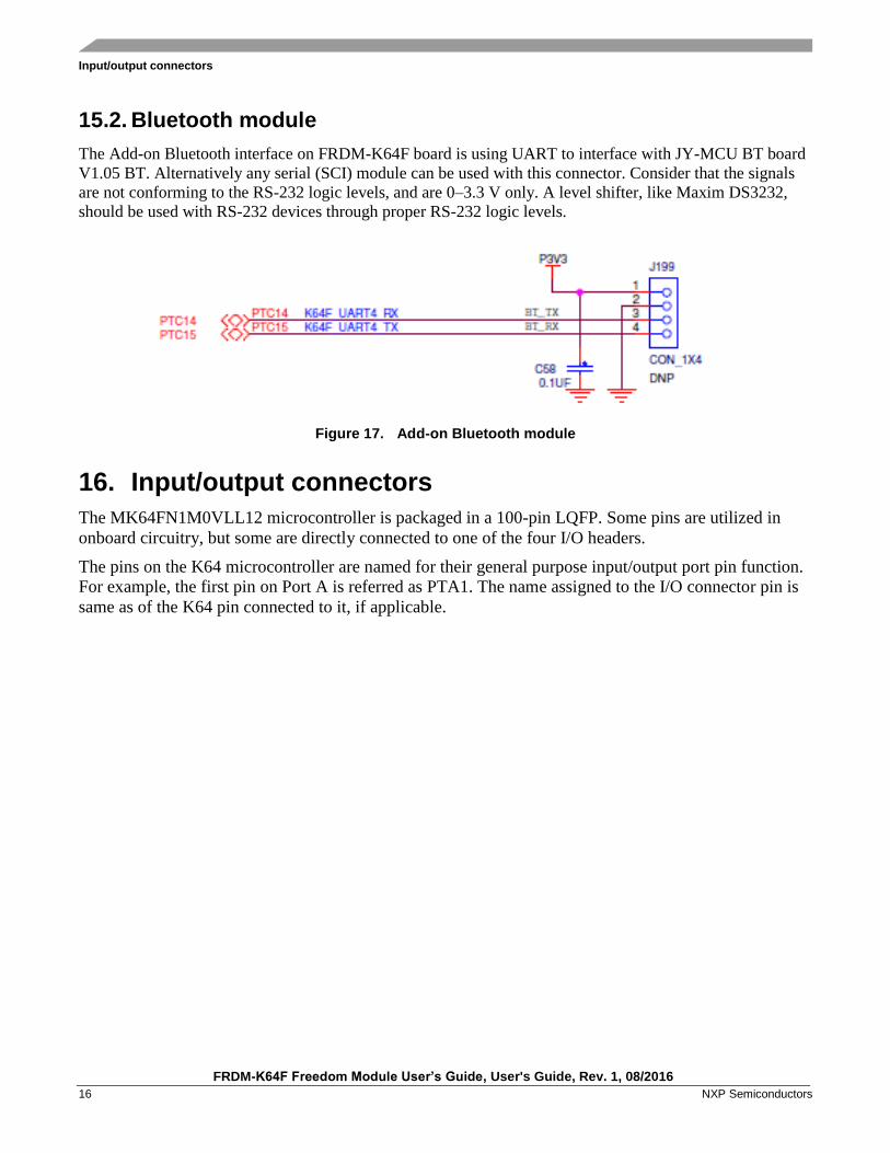
15.2. Bluetooth module
The Add-on Bluetooth interface on FRDM-K64F board is using UART to interface with JY-MCU BT board
V1.05 BT. Alternatively any serial (SCI) module can be used with this connector. Consider that the signals
are not conforming to the RS-232 logic levels, and are 0–3.3 V only. A level shifter, like Maxim DS3232,
should be used with RS-232 devices through proper RS-232 logic levels.
Figure 17. Add-on Bluetooth module
16. Input/output connectors
The MK64FN1M0VLL12 microcontroller is packaged in a 100-pin LQFP. Some pins are utilized in
onboard circuitry, but some are directly connected to one of the four I/O headers.
The pins on the K64 microcontroller are named for their general purpose input/output port pin function.
For example, the first pin on Port A is referred as PTA1. The name assigned to the I/O connector pin is
same as of the K64 pin connected to it, if applicable.
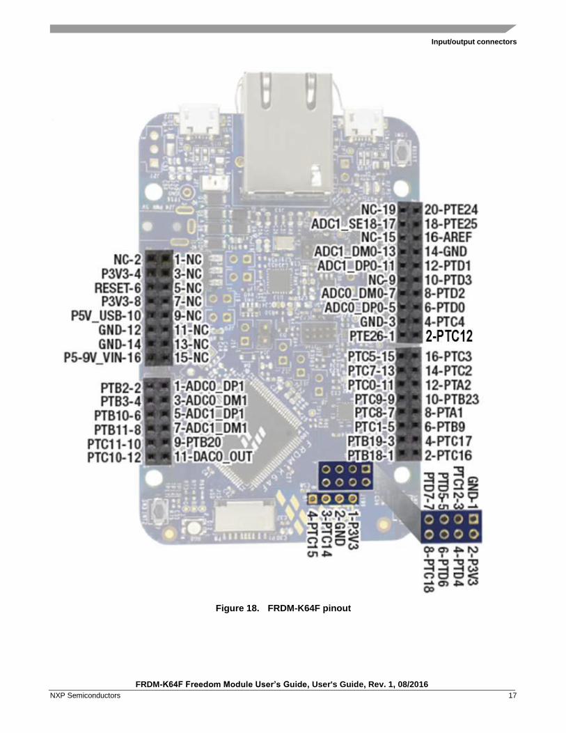
Input/output connectors
FRDM-K64F Freedom Module User’s Guide, User's Guide, Rev. 1, 08/2016
NXP Semiconductors 17
Figure 18. FRDM-K64F pinout
Revision History
FRDM-K64F Freedom Module User’s Guide, User's Guide, Rev. 1, 08/2016
18 NXP Semiconductors
17. Arduino Compatibility
The I/O headers on the FRDM-K64F board are arranged to enable compatibility with peripheral boards
(known as shields) that connect to Arduino and Arduino-compatible microcontroller boards. The outer
rows of pins (even numbered pins) on the headers, share the same mechanical spacing and placement
with the I/O headers on the Arduino Revision 3 (R3) standard.
18. References
The following references are available on nxp.com:
• FRDMK64FQSG, FRDM-K64F Quick Start Guide
• FRDM-K64F Pinouts
• FRDM-K64F-SCH, FRDM-K64F Schematic
• FRDM-K64F Design Package
19. Revision History Table 8. Revision history
Revision number Date Substantive changes
0 06/2015 Initial release
1 08/2016 • Update Table 6
• Add a not in Debug

Document Number: FRDMK64FUG Rev. 1
08/2016
How to Reach Us:
Home Page:
nxp.com
Web Support:
nxp.com/support
Information in this document is provided solely to enable system and software
implementers to use NXP products. There are no express or implied copyright licenses
granted hereunder to design or fabricate any integrated circuits based on the
information in this document. NXP reserves the right to make changes without further
notice to any products herein.
NXP makes no warranty, representation, or guarantee regarding the suitability of its
products for any particular purpose, nor does NXP assume any liability arising out of
the application or use of any product or circuit, and specifically disclaims any and all
liability, including without limitation consequential or incidental damages. “Typical”
parameters that may be provided in NXP data sheets and/or specifications can and do
vary in different applications, and actual performance may vary over time. All operating
parameters, including “typicals,” must be validated for each customer application by
customer’s technical experts. NXP does not convey any license under its patent rights
nor the rights of others. NXP sells products pursuant to standard terms and conditions
of sale, which can be found at the following address: nxp.com/SalesTermsandConditions.
NXP, the NXP logo, and Kinetis are trademarks of NXP Semiconductor, Inc., Reg. U.S.
Pat. & Tm. Off. Xtrinsic is trademark of NXP Semiconductor, Inc. All other product or
service names are the property of their respective owners. ARM and Cortex are
registered trademarks of ARM Limited (or its subsidiaries) in the EU and/or elsewhere.
mbed is a trademark of ARM Limited (or its subsidiaries) in the EU and/or elsewhere.
All rights reserved
© 2016 NXP B.V.