Embed Size (px)
Citation preview
www.advmat.dewww.MaterialsViews.com
CO
MM
UN
ICATIO
N
Tomoyuki Yokota , Kazunori Kuribara , Takeyoshi Tokuhara , Ute Zschieschang , Hagen Klauk , Kazuo Takimiya , Yuji Sadamitsu , Masahiro Hamada , Tsuyoshi Sekitani , and Takao Someya *
Flexible Low-Voltage Organic Transistors with High Thermal Stability at 250 ° C
Recently, organic thin-fi lm transistors (TFTs) have attracted considerable attention in next-generation electronic applica-tions such as fl exible displays, [ 1–3 ] large-area sensors, [ 4–7 ] and radio-frequency identifi cation tags. [ 8 , 9 ] Organic TFTs possess many advantages such as large area, low cost, and mechanical fl exibility. They can be fabricated on plastic fi lms using a solu-tion process such as a printing method. [ 10 , 11 ] Owing to recent efforts, the fi eld-effect mobilities of the best organic TFTs now exceed 10 cm 2 V − 1 s − 1 , [ 12 , 13 ] and the operation voltage can be as low as 1 V. [ 14 , 15 ]
The possibility for extension to new applications requires improvements in the stability of organic transistors. In par-ticular, thermal stability has been one of the major unresolved issues because organic semiconductors are decomposed and/or sublimed at signifi cantly lower temperatures than inor-ganic semiconductors. [ 16 ] Their thermal stability is known to be improved by appropriate encapsulation layers. Indeed, organic transistors with an encapsulation layer comprising parylene and metal thin fi lms retain their electronic functionality even after exposure to temperatures as high as 140 ° C, and these transistors are sterilizable. [ 17 ] By using a heat-resistant BTBT derivative, we found that the organic transistors were func-tional with a thermal load of up to 150 ° C. [ 18 ] In order to extend brand new applications of fl exible electronics, it is important to
© 2013 WILEY-VCH Verlag Gm
T. Yokota, K. Kuribara, Prof. T. SomeyaDepartment of Applied Physics The University of Tokyo 7-3-1 Hongo, Bunkyo-ku, Tokyo 113-8656, Japan E-mail: [email protected] T. Tokuhara, Prof. T. Sekitani, Prof. T. SomeyaDepartment of Electrical Engineering The University of Tokyo Tokyo, Japan Dr. U. Zschieschang, Dr. H. KlaukMax Planck Institute for Solid State Research Stuttgart, Germany Prof. K. TakimiyaDepartment of Applied Chemistry Graduate School of Engineering Institute for Advanced Materials Research Hiroshima University Higashi-Hiroshima, Japan Dr. Y. Sadamitsu, Dr. M. HamadaR&D Planning Division Research & Developmant Group Nippon Kayaku Co.,Ltd. Kita-ku, Tokyo, Japan
DOI: 10.1002/adma.201300941
Adv. Mater. 2013, 25, 3639–3644
improve the thermal stability of organic transistors with good electronic properties including high mobility and low operating voltage.
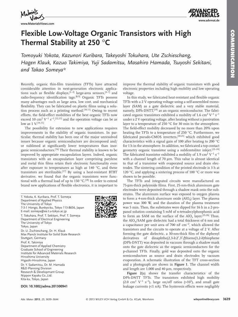
In this study, we fabricated heat-resistant and fl exible organic TFTs with a 2 V operating voltage using a self-assembled mono-layer (SAM) as a gate dielectric and a very stable material, namely, DPh-DNTT, [ 19 ] as an organic semiconductor. The fabri-cated organic transistors exhibited a mobility of 1.6 cm 2 V − 1 s − 1 under a 2 V operating voltage, after heating without a passivation layer to a temperature of 250 ° C for 30 min in the atmosphere. The fi eld-effect mobility decreased by no more than 20% upon heating the TFTs to a temperature of 250 ° C. Furthermore, we fabricated pseudo-CMOS inverters, [ 20 , 21 ] which exhibited good characteristics with a signal gain of 100 after heating to 200 ° C for 1 h in the atmosphere. In addition, we fabricated a top contact geometry organic transistor using a subfemtoliter inkjet. [ 22–24 ] The fabricated transistor exhibited a mobility of 1.9 cm 2 V − 1 s − 1 with a channel length of 70 μ m. This value is almost identical to that of a transistor with evaporated source and drain elec-trodes. The sintering condition of the printed electrode is 3 h at 120 ° C, and applying a sintering process of 100 ° C or more was shown to be possible.
The TFTs and integrated circuits were manufactured on 75- μ m-thick polyimide fi lms. First, 25-nm-thick aluminum gate electrodes were deposited through a shadow mask onto the sub-strates. The aluminum surface was exposed to oxygen plasma to form a 4-nm-thick aluminum oxide (AlO x ) layer. The plasma power was 300 W, and the duration of the plasma treatment was 5 min. Then, the substrates were dipped for 16 h in a 2-pro-panol solution containing 5 mM of n-tetradecylphosphonic acid to form an SAM on the surface of the AlO x layer. [ 25 , 26 ] Thus, the AlO x /SAM gate dielectric had a total thickness of 6 nm and a capacitance per unit area of 700 nF cm − 2 , which allowed the transistors and the circuits to operate at a voltage of 2 V. After forming the gate dielectric, a 30-nm-thick fi lm of the diphenyl derivatives of dinaphtho[2,3- b :2 ′ ,3 ′ - f ]thieno[3,2- b ]thiophene (DPh-DNTT) was deposited in vacuum through a shadow mask onto the gate dielectric as the organic semiconductors for the p-channel TFTs. Finally, gold was deposited onto the organic semiconductors as source and drain electrodes by vacuum evaporation. A schematic illustration of the TFT cross-section and a photograph are shown in Figure 1 . The channel width and length are 1,000 and 40 μ m, respectively.
Figure 2 (a) shows the transfer characteristics of the DPh-DNTT TFTs. The transistors exhibited high mobility (2.0 cm 2 V − 1 s − 1 ), large on/off ratios ( > 10 5 ), and small gate leakage currents ( < 1 nA). The hysteresis effects were negligibly
bH & Co. KGaA, Weinheim 3639wileyonlinelibrary.com

36
www.advmat.dewww.MaterialsViews.com
CO
MM
UN
ICATI
ON
Figure 1 . Structure and microscopy images of the organic transistors. (a) Schematic cross-section of the organic TFTs with patterned Al gates, ultrathin AlO x /SAM gate dielectric, vac-uum-deposited DPh-DNTT as a semiconductor, and Au source/drain contacts. The channel length and width are 40 μ m and 1,000 μ m, respectively. (b) Optical microscope image of the DPh-DNTT transistor. (c) Chemical structure of the organic semiconductor DPh-DNTT and n-tetradecylphosphonic acid (C14-SAM). (d) Transfer characteristics of the DPh-DNTT TFTs. (e) Output characteristics of the DPh-DNTT TFT.
small. The output characteristics of the DPh-DNTT TFT are shown in Figure 2 (b), which shows good saturation of the drain current.
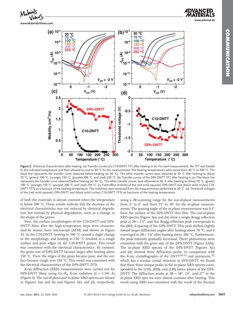
Next, we measured the thermal stability of the TFTs. All electrical measurements and the heating process were car-ried out in ambient air. We measured the electrical charac-teristics at 30 ° C after heating to various temperatures; the target heating temperature was varied from 40 ° C to 300 ° C in steps of 10 ° C. Figure 3 shows the transfer characteristics after heating. In this experiment, we measured the thermal sta-bility for two types of DNTT derivatives, namely, DPh-DNTT and 2,9-didecyldinaphtho[2,3- b :20,30- f ]thieno[3,2- b ]thiophene (C10-DNTT). [ 19 ] Figure 2 shows that the threshold voltage of
40 wileyonlinelibrary.com © 2013 WILEY-VCH Verlag GmbH & Co. KGaA, We
the DPh-DNTT TFTs shifted more toward the negative direction with an increase in the temperature. However, the change in mobility was very small [Figure 2 (a)]. On the other hand, the mobility of the C10-DNTT TFTs degraded gradually after heating above 70 ° C [Figure 2 (b)].
The mobilities and threshold voltages of both the DPh-DNTT and C10-DNTT TFTs are shown in Figure 2 (c) as functions of the temperature stress. The mobility of the C10-DNTT TFTs decreased by 45% when heated to 70 ° C. By contrast, the DPh-DNTT TFTs exhibited a high mobility of 1.6 cm 2 V − 1 s − 1 after heating to 250 ° C, and the change in mobility was as small as 23%. This experi-ment demonstrated that DPh-DNTT TFTs are signifi cantly more stable at elevated tempera-tures than the C10-DNTT TFTs. Furthermore, the thermal stability of 15 DPh-DNTT TFT devices is shown in Figure S1. The mobility changed by approximately 17% after heating to 240 ° C, and the threshold voltage gradu-ally shifted toward the negative direction with an increase in temperature. The shift in the threshold voltage observed in this experiment is consistent with that presented in the pre-vious report and can be ascribed mainly to a reduction in the number of charge trap sites originating from thermal stimulation. [ 17 , 26 , 27 ]
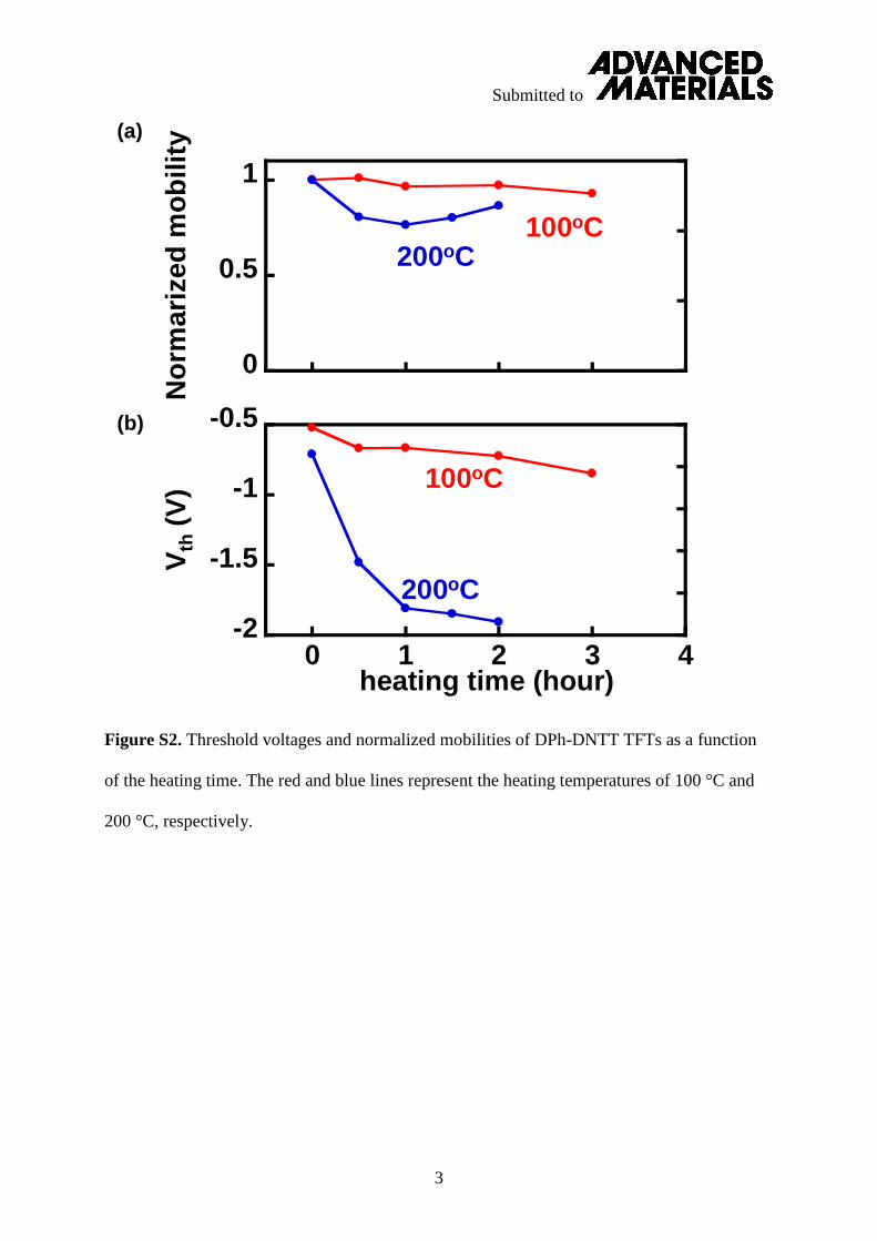
Furthermore, we evaluated the effects of the heating duration at 100 ° C and 200 ° C. Figure S2 shows the mobility and threshold voltage of the transistors after heating. In this fi gure, the red and the blue dots represent the characteristics of the transistor after heating at 100 ° C and 200 ° C, respectively. The mobility was changed by 3% and 14% after annealing for 2 hours at 100 ° C and 200 ° C, respectively. Additionally, the threshold voltage was shifted–0.2 V and –1.2 V after annealing for 2 hours at 100 ° C and 200 ° C, respectively.
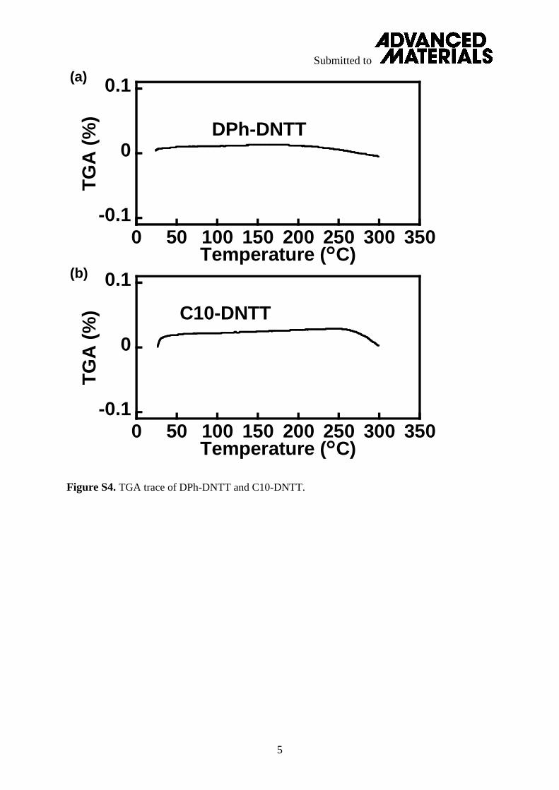
In order to evaluate the thermal stability of the molecules of organic semiconduc-tors, DPh-DNTT and C10-DNTT, we used
differential scanning calorimetry (DSC) (Shimadzu, DSC-60) and thermal gravimetric analysis (TGA) (Shimadzu, TGA-50). Figure S3 shows the DSC of the DPh-DNTT and C10-DNTT. When the DSC was run from 25 ° C to 300 ° C, DPh-DNTT did not show a peak, whereas two peaks were observed in C10-DNTT, as shown in the Figure S3. The endothermic peaks at 118 ° C and 227 ° C corresponded to the phase transition and the melting of the compound, respectively. The exothermic peak at 250 ° C corresponded to the material decomposition. These results are similar to those obtained for the oligothiophene group, where phenyl-substituted compounds exhibit better thermal stability than alkyl-substituted compounds. [ 28 , 29 ] Figure S4 shows the TGA for DPh-DNTT and C10-DNTT. The weight
inheim Adv. Mater. 2013, 25, 3639–3644
www.advmat.dewww.MaterialsViews.com
CO
MM
UN
ICATIO
N
Figure 2 . Electrical characteristics after heating. (a) Transfer curves of a C10-DNTT TFT after heating in air. For each measurement, the TFT was heated to the indicated temperature and then allowed to cool to 30 ° C for the measurement. The heating temperatures were varied from 40 ° C to 300 ° C. The black line represents the transfer curve obtained before heating (to 30 ° C). The other transfer curves were obtained at 30 ° C after heating to (blue) 70 ° C, (green) 100 ° C, (orange) 150 ° C, (purple) 200 ° C, and (red) 250 ° C. (b) Transfer curves of the DPh-DNTT TFT after heating in air. The black line represents the transfer curve obtained before heating (to 30 ° C). The other transfer curves were obtained at 30 ° C after heating to (blue) 70 ° C, (green) 100 ° C, (orange) 150 ° C, (purple) 200 ° C, and (red) 250 ° C. (c) Field-effect mobility of the (red solid squares) DPh-DNTT and (black solid circles) C10-DNTT TFTs as a function of the heating temperature. The mobilities were extracted from the measurements performed at 30 ° C. (d) Threshold voltages of the (red solid squares) DPh-DNTT and (black solid circles) C10-DNTT TFTs as functions of the heating temperature.
10-14
10-12
10-10
10-8
10-6
10-4
-2-10
-ID
S (
A)
VGS (V)
VDS = -2 V
30 oC70 oC100 oC150 oC200 oC250 oC
10-14
10-12
10-10
10-8
10-6
10-4
-2-10
-ID
S (
A)
VGS (V)
VDS = -2 V
30 oC70 oC100 oC150 oC200 oC250 oC
(a) (b)
0
0.5
1
1.5
2
2.5
0 50 100 150 200 250 300
Mo
bil
ity (
cm
2/V
s)
Temperature (° C)
DPh-DNTT
C10-DNTT
-2
-1.5
-1
-0.5
0
0 50 100 150 200 250 300
Th
resh
old
vo
ltag
e (
V)
Temperature (° C)
DPh-DNTT
C10-DNTT
(c) (d)
of both the materials is almost constant when the temperature is below 200 ° C. These results indicate that the decrease in the electrical characteristics was not induced by chemical degrada-tion but instead by physical degradation, such as a change in the shape of the grains.
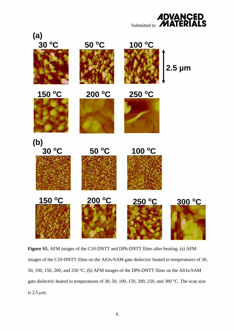
Next, the surface morphologies of the C10-DNTT and DPh-DNTT fi lms after the high-temperature steps were character-ized by atomic force microscopy (AFM) and shown in Figure S5. In the C10-DNTT, heating to 100 ° C caused a slight change in the morphology, and heating to 150 ° C resulted in a rough surface and poor edges on the C10-DNTT grains. This result was consistent with the electrical characteristics. By contrast, the grain size of DPh-DNTT became larger after heating above 150 ° C. Then, the edges of the grain became poor, and the sur-face became rough over 250 ° C. This result was consistent with the electrical characteristics of the DPh-DNTT TFTs.
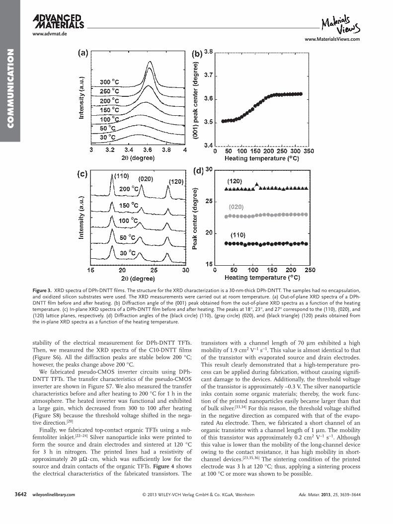
X-ray diffraction (XRD) measurements were carried out for DPh-DNTT fi lms using Cu–K α X-ray radiation ( λ = 1.541 Å) (Figure 3 ). The out-of-plane and in-plane XRD spectra are shown in Figures 3 (a) and (b) and Figures 3 (c) and (d), respectively,
© 2013 WILEY-VCH Verlag GAdv. Mater. 2013, 25, 3639–3644
using a 2 θ scanning range for the out-of-plane measurements from 3 ° to 4 ° and from 15 ° to 30 ° for the in-plane measure-ments. The grazing angle of the in-plane measurement was 0.2 ° from the surface of the DPh-DNTT thin fi lm. The out-of-plane XRD spectra [Figure 3 (a) and (b)] show a single Bragg refl ection peak at 2 θ = 3.5 ° , and this Bragg refl ection peak corresponds to the (001) d -spacing of the DPh-DNTT. This peak shifted slightly toward larger diffraction angles after heating above 70 ° C, and it converged to 2 θ = 3.6 ° after heating above 200 ° C. Furthermore, the peak intensity gradually increased. These phenomena were consistent with the grain size of the DPh-DNTT [Figure S2(b)]. The in-plane XRD spectra of the DPh-DNTT [Figures 3 (c) and (d)] showed three diffraction peaks. In comparison with the X-ray crystallography of the DNTT [ 30 , 31 ] and pentacene, [ 32 ] which has a similar crystal structure to DPh-DNTT, we found that these three unique peaks in the in-plane XRD spectra corre-sponded to the (110), (020), and (120) lattice planes of the DPh-DNTT. The diffraction peaks at 2 θ = 18 ° , 23 ° , and 27 ° in the in-plane XRD spec-tra were almost constant after heating. This result using XRD was consistent with the result of the thermal
3641wileyonlinelibrary.commbH & Co. KGaA, Weinheim
3642
www.advmat.dewww.MaterialsViews.com
CO
MM
UN
ICATI
ON
Figure 3 . XRD spectra of DPh-DNTT fi lms. The structure for the XRD characterization is a 30-nm-thick DPh-DNTT. The samples had no encapsulation, and oxidized silicon substrates were used. The XRD measurements were carried out at room temperature. (a) Out-of-plane XRD spectra of a DPh-DNTT fi lm before and after heating. (b) Diffraction angle of the (001) peak obtained from the out-of-plane XRD spectra as a function of the heating temperature. (c) In-plane XRD spectra of a DPh-DNTT fi lm before and after heating. The peaks at 18 ° , 23 ° , and 27 ° correspond to the (110), (020), and (120) lattice planes, respectively. (d) Diffraction angles of the (black circle) (110), (gray circle) (020), and (black triangle) (120) peaks obtained from the in-plane XRD spectra as a function of the heating temperature.
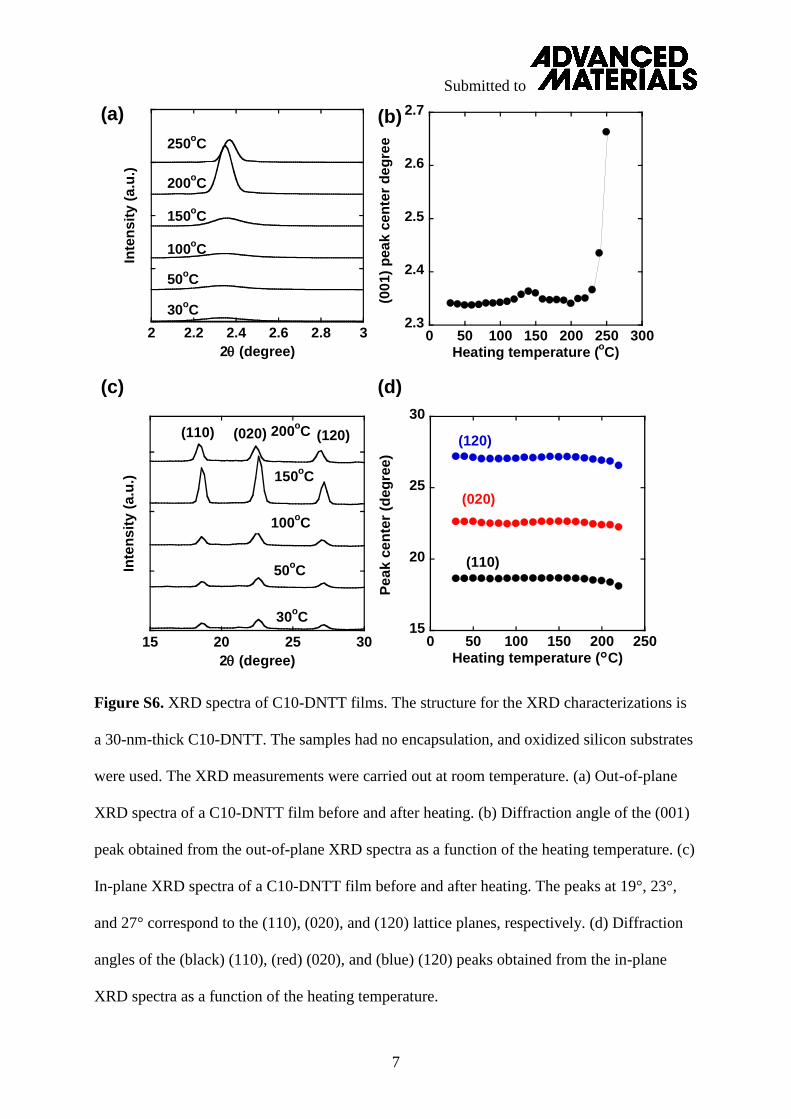
stability of the electrical measurement for DPh-DNTT TFTs. Then, we measured the XRD spectra of the C10-DNTT fi lms (Figure S6). All the diffraction peaks are stable below 200 ° C; however, the peaks change above 200 ° C.
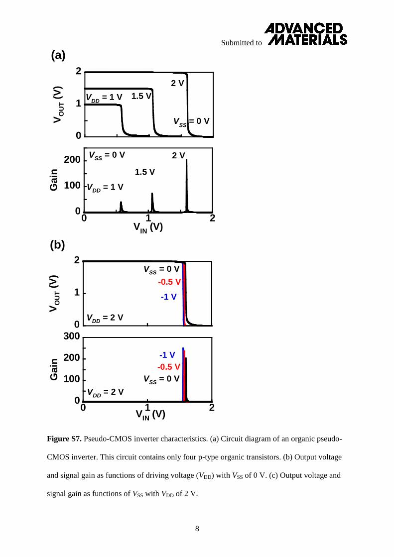
We fabricated pseudo-CMOS inverter circuits using DPh-DNTT TFTs. The transfer characteristics of the pseudo-CMOS inverter are shown in Figure S7. We also measured the transfer characteristics before and after heating to 200 ° C for 1 h in the atmosphere. The heated inverter was functional and exhibited a large gain, which decreased from 300 to 100 after heating (Figure S8) because the threshold voltage shifted in the nega-tive direction. [ 20 ]
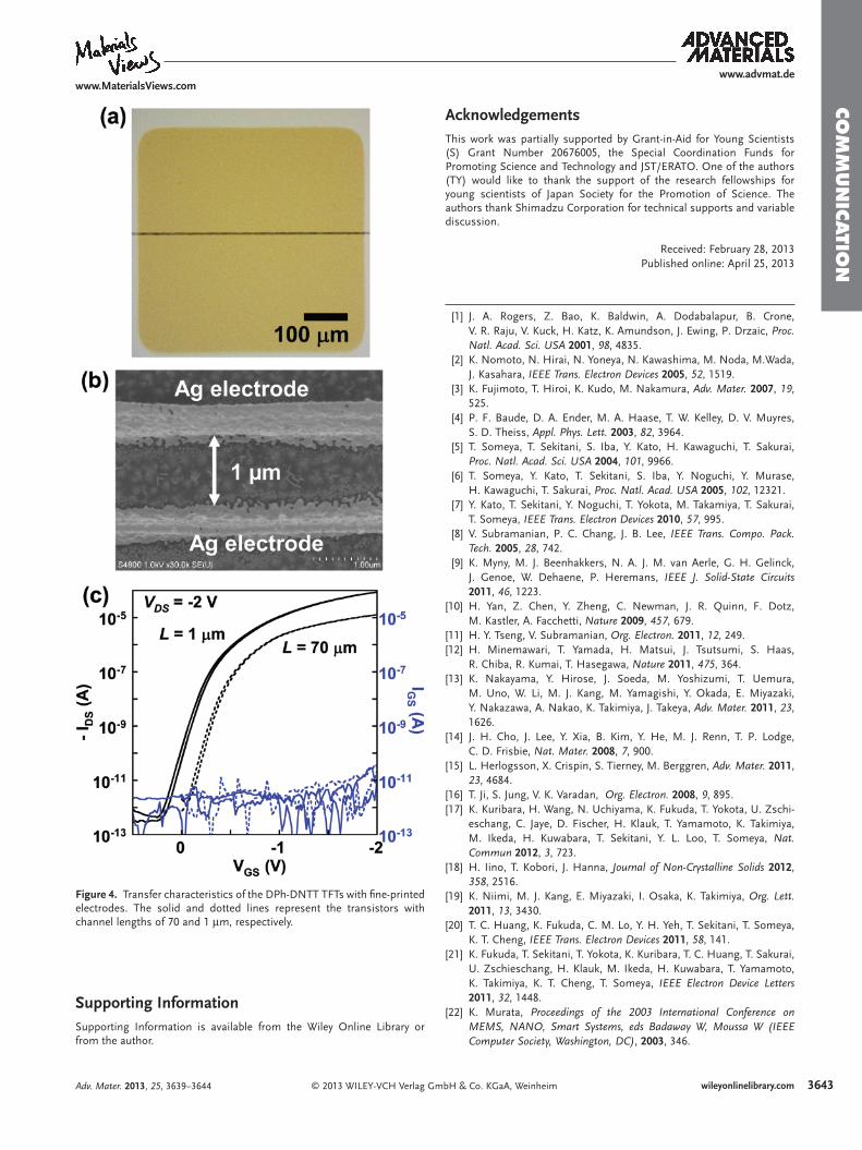
Finally, we fabricated top-contact organic TFTs using a sub-femtoliter inkjet. [ 22–24 ] Silver nanoparticle inks were printed to form the source and drain electrodes and sintered at 120 ° C for 3 h in nitrogen. The printed lines had a resistivity of approximately 20 μ Ω · cm, which was suffi ciently low for the source and drain contacts of the organic TFTs. Figure 4 shows the electrical characteristics of the fabricated transistors. The
wileyonlinelibrary.com © 2013 WILEY-VCH Verlag Gm
transistors with a channel length of 70 μ m exhibited a high mobility of 1.9 cm 2 V − 1 s − 1 . This value is almost identical to that of the transistor with evaporated source and drain electrodes. This result clearly demonstrated that a high-temperature pro-cess can be applied during fabrication, without causing signifi -cant damage to the devices. Additionally, the threshold voltage of the transistor is approximately –0.3 V. The silver nanoparticle inks contain some organic materials; thereby, the work func-tion of the printed nanoparticles easily became larger than that of bulk silver. [ 33 , 34 ] For this reason, the threshold voltage shifted in the negative direction as compared with that of the evapo-rated Au electrode. Then, we fabricated a short channel of an organic transistor with a channel length of 1 μ m. The mobility of this transistor was approximately 0.2 cm 2 V − 1 s − 1 . Although this value is lower than the mobility of the long-channel device owing to the contact resistance, it has high mobility in short-channel devices. [ 23 , 35 , 36 ] The sintering condition of the printed electrode was 3 h at 120 ° C; thus, applying a sintering process at 100 ° C or more was shown to be possible.
bH & Co. KGaA, Weinheim Adv. Mater. 2013, 25, 3639–3644
www.advmat.dewww.MaterialsViews.com
CO
MM
UN
ICATIO
N
Figure 4 . Transfer characteristics of the DPh-DNTT TFTs with fi ne-printed electrodes. The solid and dotted lines represent the transistors with channel lengths of 70 and 1 μ m, respectively.
Supporting Information Supporting Information is available from the Wiley Online Library or from the author.
© 2013 WILEY-VCH Verlag GmAdv. Mater. 2013, 25, 3639–3644
Acknowledgements This work was partially supported by Grant-in-Aid for Young Scientists (S) Grant Number 20676005, the Special Coordination Funds for Promoting Science and Technology and JST/ERATO. One of the authors (TY) would like to thank the support of the research fellowships for young scientists of Japan Society for the Promotion of Science. The authors thank Shimadzu Corporation for technical supports and variable discussion.
Received: February 28, 2013 Published online: April 25, 2013
[ 1 ] J. A. Rogers , Z. Bao , K. Baldwin , A. Dodabalapur , B. Crone , V. R. Raju , V. Kuck , H. Katz , K. Amundson , J. Ewing , P. Drzaic , Proc. Natl. Acad. Sci. USA 2001 , 98 , 4835 .
[ 2 ] K. Nomoto , N. Hirai , N. Yoneya , N. Kawashima , M. Noda , M.Wada , J. Kasahara , IEEE Trans. Electron Devices 2005 , 52 , 1519 .
[ 3 ] K. Fujimoto , T. Hiroi , K. Kudo , M. Nakamura , Adv. Mater. 2007 , 19 , 525 .
[ 4 ] P. F. Baude , D. A. Ender , M. A. Haase , T. W. Kelley , D. V. Muyres , S. D. Theiss , Appl. Phys. Lett. 2003 , 82 , 3964 .
[ 5 ] T. Someya , T. Sekitani , S. Iba , Y. Kato , H. Kawaguchi , T. Sakurai , Proc. Natl. Acad. Sci. USA 2004 , 101 , 9966 .
[ 6 ] T. Someya , Y. Kato , T. Sekitani , S. Iba , Y. Noguchi , Y. Murase , H. Kawaguchi , T. Sakurai , Proc. Natl. Acad. USA 2005 , 102 , 12321 .
[ 7 ] Y. Kato , T. Sekitani , Y. Noguchi , T. Yokota , M. Takamiya , T. Sakurai , T. Someya , IEEE Trans. Electron Devices 2010 , 57 , 995 .
[ 8 ] V. Subramanian , P. C. Chang , J. B. Lee , IEEE Trans. Compo. Pack. Tech. 2005 , 28 , 742 .
[ 9 ] K. Myny , M. J. Beenhakkers , N. A. J. M. van Aerle , G. H. Gelinck , J. Genoe , W. Dehaene , P. Heremans , IEEE J. Solid-State Circuits 2011 , 46 , 1223 .
[ 10 ] H. Yan , Z. Chen , Y. Zheng , C. Newman , J. R. Quinn , F. Dotz , M. Kastler , A. Facchetti , Nature 2009 , 457 , 679 .
[ 11 ] H. Y. Tseng , V. Subramanian , Org. Electron. 2011 , 12 , 249 . [ 12 ] H. Minemawari , T. Yamada , H. Matsui , J. Tsutsumi , S. Haas ,
R. Chiba , R. Kumai , T. Hasegawa , Nature 2011 , 475 , 364 . [ 13 ] K. Nakayama , Y. Hirose , J. Soeda , M. Yoshizumi , T. Uemura ,
M. Uno , W. Li , M. J. Kang , M. Yamagishi , Y. Okada , E. Miyazaki , Y. Nakazawa , A. Nakao , K. Takimiya , J. Takeya , Adv. Mater. 2011 , 23 , 1626 .
[ 14 ] J. H. Cho , J. Lee , Y. Xia , B. Kim , Y. He , M. J. Renn , T. P. Lodge , C. D. Frisbie , Nat. Mater. 2008 , 7 , 900 .
[ 15 ] L. Herlogsson , X. Crispin , S. Tierney , M. Berggren , Adv. Mater. 2011 , 23 , 4684 .
[ 16 ] T. Ji , S. Jung , V. K. Varadan , Org. Electron. 2008 , 9 , 895 . [ 17 ] K. Kuribara , H. Wang , N. Uchiyama , K. Fukuda , T. Yokota , U. Zschi-
eschang , C. Jaye , D. Fischer , H. Klauk , T. Yamamoto , K. Takimiya , M. Ikeda , H. Kuwabara , T. Sekitani , Y. L. Loo , T. Someya , Nat. Commun 2012 , 3 , 723 .
[ 18 ] H. Iino , T. Kobori , J. Hanna , Journal of Non-Crystalline Solids 2012 , 358 , 2516 .
[ 19 ] K. Niimi , M. J. Kang , E. Miyazaki , I. Osaka , K. Takimiya , Org. Lett. 2011 , 13 , 3430 .
[ 20 ] T. C. Huang , K. Fukuda , C. M. Lo , Y. H. Yeh , T. Sekitani , T. Someya , K. T. Cheng , IEEE Trans. Electron Devices 2011 , 58 , 141 .
[ 21 ] K. Fukuda , T. Sekitani , T. Yokota , K. Kuribara , T. C. Huang , T. Sakurai , U. Zschieschang , H. Klauk , M. Ikeda , H. Kuwabara , T. Yamamoto , K. Takimiya , K. T. Cheng , T. Someya , IEEE Electron Device Letters 2011 , 32 , 1448 .
[ 22 ] K. Murata , Proceedings of the 2003 International Conference on MEMS, NANO, Smart Systems, eds Badaway W, Moussa W (IEEE Computer Society, Washington, DC) , 2003 , 346 .
3643wileyonlinelibrary.combH & Co. KGaA, Weinheim
364
www.advmat.de
CO
MM
UN
ICATI
ON
[ 23 ] T. Sekitani , Y. Noguchi , U. Zschieschang , H. Klauk , T. Someya , Proc.Nat. Acad. Sci. 2008 , 105 , 4976 . [ 24 ] T. Yokota , T. Sekitani , Y. Kato , K. Kuribara , U. Zschieschang ,
H. Klauk , T. Yamamoto , K. Takimiya , H. Kuwabara , M. Ikeda , T. Someya , MRS Commun. 2011 , 1 , 3 .
[ 25 ] H. Klauk , U. Zschieschang , J. Pfl aum , M. Halik , Nature 2007 , 445 , 745 .
[ 26 ] K. Fukuda , T. Yokota , K. Kuribara , T. Sekitani , U. Zschieschang , H. Klauk , T. Someya , Appl. Phys. Lett. 2010 , 96 , 053302 .
[ 27 ] K. Fukuda , T. Sekitani , T. Someya , Appl. Phys. Lett. 2009 , 95 , 023302 . [ 28 ] A. Facchetti , J. Letizia , M. H. Yoon , M. Mushrush , H. E. Katz ,
T. J. Marks , Chem. Mater. 2004 , 16 , 4715 . [ 29 ] Y. Sun , Y. Ma , Y. Liu , Y. Lin , Z. Wang , Y. Wang , C. Di , K. Xiao ,
X. Chen , W. Qiu , B. Zhang , G. Yu , W. Hu , D. Zhu , Adv. Funct. Mater. 2006 , 16 , 426 .
4 wileyonlinelibrary.com © 2013 WILEY-VCH Verlag Gm
www.MaterialsViews.com
[ 30 ] T. Yamamoto , K. Takimiya , J. Am. Chem. Soc. 2007 , 129 , 2224 . [ 31 ] T. Yamamoto , S. Shinamura , E. Miyazaki , K. Takimiya , Bull. Chem.
Soc. Jpn. 2010 , 83 , 120 . [ 32 ] C. C. Mattheus , A. B. Dros , J. Baas , A. Meetsma , J. L. de Boer ,
T. T. M. Palstra , Acta Cryst. 2001 , C57 , 939 . [ 33 ] S. Narioka , H. Ishii , D. Yoshimura , M. Sei , Y. Ouchi , K. Seki ,
S. Hasegawa , T. Miyazaki , Y. Harima , K. Yamashita , Appl. Phys. Lett. 1995 , 67 , 1899 .
[ 34 ] D. Kim , S. Jeong , H. Shin , Y. Xia , J. Moon , Adv. Mater. 2008 , 20 , 3084 . [ 35 ] C. Auner , U. Palfi nger , H. Gold , J. Kraxner , A. Haase , T. Haber ,
M. Sezen , W. Grogger , G. Jakopic , J. R. Krenn , G. Leising , B. Stadlober , Org. Electron. 2009 , 10 , 1466 .
[ 36 ] F. Ante , D. Kälblein , T. Zaki , U. Zschieschang , K. Takimiya , M. Ikeda , T. Sekitani , T. Someya , J. N. Burghartz , K. Kern , H. Klauk , Small 2012 , 8 , 73 .
bH & Co. KGaA, Weinheim Adv. Mater. 2013, 25, 3639–3644
Submitted to
1
DOI: 10.1002/adma. 201300941
Flexible low-voltage organic transistors with high thermal stability at 250 °C
By Tomoyuki Yokota, Kazunori Kuribara, Takeyoshi Tokuhara, Ute Zschieschang, Hagen
Klauk, Kazuo Takimiya, Yuji Sadamitsu , Masahiro Hamada, Tsuyoshi Sekitani, and Takao
Someya*
[*] Prof. T. Someya, T. Yokota, K. Kuribara
Department of Applied Physics, The University of Tokyo
7-3-1 Hongo, Bunkyo-ku, Tokyo 113-8656, Japan
E-mail: [email protected]
T. Tokuhara, Prof. T. Sekitani, Prof. T. Someya
Department of Electrical Engineering, The University of Tokyo,
Tokyo, Japan
Dr. U. Zschieschang, Dr. H. Klauk
Max Planck Institute for Solid State Research,
Stuttgart, Germany
Prof. K. Takimiya
Department of Applied Chemistry,
Graduate School of Engineering,
Institute for Advanced Materials Research,
Hiroshima University,
Higashi-Hiroshima, Japan
Dr. Y. Sadamitsu , Dr. M. Hamada
R&D Planning Division
Research & Developmant Group
Nippon Kayaku Co.,Ltd., Kita-ku, Tokyo, Japan
Keywords: Thermal stability, Organic Field-Effect Transistors, Organic Electronics, Self-
Assembled Monolayer

Submitted to
2
Supporting information
Figure S1. Threshold voltages and normalized mobilities of 15 DPh-DNTT TFTs as a
function of the heating temperature. The red and blue solid circles show the mobility and
threshold voltage of the DPh-DNTT TFTs, respectively.
0
0.5
1
1.5
-2.5
-2
-1.5
-1
-0.5
0 50 100 150 200 250 300
No
rmali
ze
d m
ob
ilit
yV
TH (V
)
Temperature (°C)
Submitted to
3
Figure S2. Threshold voltages and normalized mobilities of DPh-DNTT TFTs as a function
of the heating time. The red and blue lines represent the heating temperatures of 100 °C and
200 °C, respectively.
0
0.5
1N
orm
ari
zed
mo
bilit
y
100oC200oC
-2
-1.5
-1
-0.5
0 1 2 3 4
Vth
(V
)
heating time (hour)
100oC
200oC
(a)
(b)

Submitted to
4
Figure S3. DSC trace of DPh-DNTT and C10-DNTT.
-5
-2.5
0
2.5
5
0 50 100 150 200 250 300 350
DS
C (
mW
)
Temperature (°C)
DPh-DNTT
-5
-2.5
0
2.5
5
0 50 100 150 200 250 300 350
DS
C (
mW
)
Temperature (°C)
C10-DNTT
(a)
(b)
Submitted to
5
Figure S4. TGA trace of DPh-DNTT and C10-DNTT.
-0.1
0
0.1
0 50 100 150 200 250 300 350
TG
A (
%)
Temperature (°C)
DPh-DNTT
-0.1
0
0.1
0 50 100 150 200 250 300 350
TG
A (
%)
Temperature (°C)
C10-DNTT
(a)
(b)
Submitted to
6
Figure S5. AFM images of the C10-DNTT and DPh-DNTT films after heating. (a) AFM
images of the C10-DNTT films on the AlOx/SAM gate dielectric heated to temperatures of 30,
50, 100, 150, 200, and 250 °C. (b) AFM images of the DPh-DNTT films on the AlOx/SAM
gate dielectric heated to temperatures of 30, 50, 100, 150, 200, 250, and 300 °C. The scan size
is 2.5 m.
(b)
30 oC 50 oC 100 oC
150 oC 200 oC 250 oC
30 oC 50 oC 100 oC
150 oC 200 oC 250 oC 300 oC
(a)
2.5 µm
Submitted to
7
Figure S6. XRD spectra of C10-DNTT films. The structure for the XRD characterizations is
a 30-nm-thick C10-DNTT. The samples had no encapsulation, and oxidized silicon substrates
were used. The XRD measurements were carried out at room temperature. (a) Out-of-plane
XRD spectra of a C10-DNTT film before and after heating. (b) Diffraction angle of the (001)
peak obtained from the out-of-plane XRD spectra as a function of the heating temperature. (c)
In-plane XRD spectra of a C10-DNTT film before and after heating. The peaks at 19°, 23°,
and 27° correspond to the (110), (020), and (120) lattice planes, respectively. (d) Diffraction
angles of the (black) (110), (red) (020), and (blue) (120) peaks obtained from the in-plane
XRD spectra as a function of the heating temperature.
2.3
2.4
2.5
2.6
2.7
0 50 100 150 200 250 300
(00
1)
pea
k c
en
ter
de
gre
e
Heating temperature (oC)
2 2.2 2.4 2.6 2.8 3
Inte
ns
ity
(a
.u.)
2 (degree)
30oC
50oC
100oC
150oC
200oC
250oC
15 20 25 30
Inte
ns
ity
(a
.u.)
2 (degree)
30oC
50oC
100oC
150oC
200oC(110) (020) (120)
15
20
25
30
0 50 100 150 200 250
Pe
ak
ce
nte
r (d
eg
ree)
Heating temperature (°C)
(110)
(020)
(120)
(a)
(c)
(b)
(d)
Submitted to
8
Figure S7. Pseudo-CMOS inverter characteristics. (a) Circuit diagram of an organic pseudo-
CMOS inverter. This circuit contains only four p-type organic transistors. (b) Output voltage
and signal gain as functions of driving voltage (VDD) with VSS of 0 V. (c) Output voltage and
signal gain as functions of VSS with VDD of 2 V.
0
1
2
VO
UT (
V)
VSS = 0 V
-1 V
VDD = 2 V
-0.5 V
0
100
200
0 1 2
Gain
VSS = 0 V 2 V
1.5 V
VDD = 1 V
VIN
(V)
0
100
200
300
0 1 2
Gain
VIN (V)
-1 V
VDD
= 2 V
-0.5 V
VSS = 0 V
0
1
2
VO
UT (
V)
VSS
= 0 V
VDD
= 1 V 1.5 V
2 V
(a)
(b)

Submitted to
9
Figure S8. Pseudo-CMOS inverter characteristics. The black and gray lines represent the
characteristics before and after heating to 200 °C for 1 h. (a) Output characteristics with a VDD
of 2 V and a VSS of –1 V before and after heating to 200 °C for 1 h. (c) Signal gain before and
after heating to 200 °C for 1 h.
0
100
200
300
0 1 2
Gain
VIN (V)
After heating
VDD = 2 V
VSS = -1 V
Before
0
1
2V
OU
T (
V)
VSS = -1 V
VDD = 2 V
After heatingBefore

![[Chapter III] Basic Knowledge of Discrete Semiconductor ......transistors (IGBTs) Power transistors (2SAxx,2SBxx,2SCxx,2SDxx, TTAxx,TTBxx,TTCxx,TTDxx) Types of Transistors Transistors](https://img.dokumen.tips/doc/110x75/5e766014341a1a707d5f4c34/chapter-iii-basic-knowledge-of-discrete-semiconductor-transistors-igbts.jpg)