Embed Size (px)
Citation preview

SPINOSA
IST-2001-33334
Spin polarized injection in nanostructures and devices
Final report Covering period 01.01.2002-12.31.2004
Report Version: 1
Report Preparation Date: 01.05.2005
Classification: Confidential
Contract Start Date: 1.1.2002 Duration: 12.31.2004
Project Co-ordinator: Wuerzburg (UWUERZ)
Partners: Nijmegen (KUN)
IMEC, Leuven (IMEC)
Bologna (ISM)
Oxford (UOXF.DK)
Twente (UT)
Warsaw (IP PAS)
Project funded by the European Community under the “Information Society Technologies” Programme (1998-2002)
SPINOSA


Table of contents
iSPINOSA
Table of contentsPart 1: Executive summary ........................................................................... 1Introduction ...............................................................................................................1Part 2: Work Progress Overview .................................................................. 5Introduction ...............................................................................................................5Deliverables ...............................................................................................................5Part 2/1: Work Progress Overview Year 1 ................................................... 7Introduction ...............................................................................................................7Tunnel barriers and manganites ................................................................................7LED with Tunnel barrier ...........................................................................................7Manganites ................................................................................................................7Preparational work ....................................................................................................7Theory........................................................................................................................8New partner ...............................................................................................................8Part 2/1a: WP1 Room temperature spin injection into semiconductors
(standard ferromagnets) ............................................................................ 9IMEC ............................................................................................................... 9Introduction ...............................................................................................................9Experiments and results ..........................................................................................10The LED structure ...................................................................................................10The oblique Hanle effect ......................................................................................... 11Results ..................................................................................................................... 11RT spin injection .....................................................................................................15Modelling ................................................................................................................15UWUERZ ...................................................................................................... 17Introduction .............................................................................................................17Optical experiments: Top emission versus side emission ......................................17Nanopatterning ........................................................................................................20Developing lithography ..........................................................................................20Magnetic nanostructures for magnetooptics ...........................................................21Tunnel contacts........................................................................................................22Fabrication ...............................................................................................................22Results .....................................................................................................................22KUN ............................................................................................................... 25Introduction .............................................................................................................25Pump-probe measurements .....................................................................................25Semiconductors .......................................................................................................25Dielectrics ................................................................................................................28Magneto-optical microscope ...................................................................................29
IST-2001-33334 SPINOSA 3rd year report
iiSPINOSA
Study of magnetization in nanostructures by magneto-optical diffraction andmicroscopy...........................................................................................................30
Pt/CoNi/Pt samples from Twente ............................................................................30Ni/Si samples from Wuerzburg ...............................................................................34Personnel and plans .................................................................................................35UT................................................................................................................... 37Introduction .............................................................................................................37Hot electron spin-filters ..........................................................................................37UOXF.DK ...................................................................................................... 39Introduction .............................................................................................................39Sample Fabrication..................................................................................................39Experimental Methods and Results ........................................................................40Discussion ...............................................................................................................41IPPAS ............................................................................................................. 47Introduction .............................................................................................................47SIMS and RBS measurements ................................................................................47Optical and SQUID characterization of (magnetic) semiconductors .....................49Epitaxial ferromagnetic metal films ........................................................................52Part 2/1b: WP 2 Manganite based contacts ............................................... 55UT................................................................................................................... 55Introduction .............................................................................................................55Experiments .............................................................................................................55CNR................................................................................................................ 57Introduction .............................................................................................................57Technology ..............................................................................................................57Experiments .............................................................................................................59Deconvolution of the manganite bands ..................................................................61UWUERZ ...................................................................................................... 65Collaboration ...........................................................................................................65Part 2/2: Work Progress Overview Year 2 ................................................. 67Iescription of work and results................................................................................67Part 2/2a: (WP1) Novel detection methods ................................................ 69Introduction .............................................................................................................69Dynamical nuclear polarization in compensation doped active layers ..................69Complementary experiments in standard geometry ...............................................73Measuring the magnetic moment ............................................................................75Detection of a magnetic moment induced by spin polarized currents using SQUID
magnetometry ......................................................................................................75The measurement setup ...........................................................................................76Ultrasensitive Magneto-Optical Detection of Electrically Injected Spins Into Bulk
Semiconductor .....................................................................................................79

Table of contents
iiiSPINOSA
Part 2/2b (WP1): Schottky barriers and hot electron injection .............. 81Introduction .............................................................................................................81Schottky tunnel barrier injectors with epitaxial MnSb contacts: magnetic
characteristics ......................................................................................................81Schottky tunnel barrier injectors with epitaxial MnSb contacts: electrical
characteristics ......................................................................................................84Dynamical nuclear polarization in MnSb-based Schottky tunnel spin LEDs ........86Structural characterization of half-Heusler compound NiMnSb by RBC technique
88Hot electron spin injectors ......................................................................................92Introduction and issues: ..........................................................................................931) Hole current ........................................................................................................942) Emitter structure .................................................................................................943) Bonding ...............................................................................................................94Results: ....................................................................................................................94Results 1) Hole current ...........................................................................................94Results 2) Emitter structure.....................................................................................95Fabrication and characterization of MIS diodes:....................................................95Integration of the MIS diode in the spin-valve transistor: .....................................96Fabrication issues for transistor with MIS diode: ..................................................98Results 3) Bonding. .................................................................................................99Discussion of the results and comparison with workplan: ...................................100Plan for the next year: ...........................................................................................100Part 2/2c: (WP1) Electrical measurements and spin injection into silicon
103Introduction ...........................................................................................................103Tunnel barriers on (Ga,Mn)As ..............................................................................103Sample Fabrication: ..............................................................................................104 a. Magnetization Measurements: .........................................................................105b. Electrical Measurements: ..................................................................................105c. Magnetoresistance Measurements: ...................................................................106d. A novel magnetoresistance effect......................................................................107Tunnel barriers on silicon .....................................................................................108Investigation of tunnel barriers using TEM..........................................................110Samples Investigated .............................................................................................113Electrical Characterization ....................................................................................115Spin injection into silicon (non local measurements) ..........................................118Spin Injection into Si (vertical measurements) .....................................................122Electrical characteristics in zero applied magnetic field ......................................122Two-terminal I-V characteristics...........................................................................122Electrical characteristics in an applied magnetic field .........................................124

IST-2001-33334 SPINOSA 3rd year report
ivSPINOSA
Two-terminal I-V characteristics...........................................................................124Three-terminal I-V characteristics ........................................................................128Micromagnetic measurements ..............................................................................129Part 2/3: Work Progress Overview Year 3 ............................................... 131Description of work and results ............................................................................131Part 2/3a (WP1): Novel detection methods .............................................. 133Introduction ...........................................................................................................133Time-Resolved Magneto-Optical Study of Epitaxial (Ga,Ma)As Films ..............133Optical Hot Electron and Spin Injection in InP: ...................................................134Ultrasensitive Magneto-Optical Detection of Spins Electrically Injected Into Bulk
Semiconductor ...................................................................................................137Giant Magnetic Linear Dichroism as a Key to the Electronic Structure of
Ferromagnetic (Ga,Mn)As ................................................................................138Magnetization switching in GaMnAs by femtosecond optical excitation ...........141Magneto-optical diffraction as a tool to study the magnetization of sub-micrometer
injecting contacts ...............................................................................................142Epitaxial Fe injectors on a Schottky tunnel barrier, and comparison between the
oblique Hanle and the Faraday geometries .......................................................144Faraday measurements ..........................................................................................144Dynamical nuclear polarization and nuclear magnetic resonance .......................145Part 2/3b (WP1): Injection through barriers and hot electron injection
147Introduction ...........................................................................................................147Results on optimized spin-LEDs ..........................................................................147Demonstration of injection of highly spin-polarized hot electrons into a
semiconductor at room temperature..................................................................147Results part 1: Hot-electron spin-injection ...........................................................148Operation of the MIS injector ...............................................................................148Bonding of complete structure with MIS emitter and AlGaAs LED ...................149a) The roughness of substrates ..............................................................................149b) Surface roughening due to Au deposition ........................................................149c) Thermal contact and thermal mismatch in cryogenic etching ..........................150Conclusions ...........................................................................................................150Results part 2: Towards spin–injection of hot holes. ............................................151Co nanoparticles ....................................................................................................153...............................................................................................................................153Part 2/3c: (WP1) Electrical measurements and spin injection into silicon
155Introduction ...........................................................................................................155Improvement of magnetic contact properties .......................................................155Using p-type silicon ..............................................................................................155

Table of contents
vSPINOSA
Optimization of the tunnel barriers at UT.............................................................156TEM studies of interfaces .....................................................................................158Theoretical modelling of barriers .........................................................................161Electrical considerations on the tunnel injector....................................................161Magnetic considerations on the tunnel injector ....................................................162Considerations on the semiconductor channel .....................................................162Electrical design of contacts for spin injection and detection in unipolar devices
163Tunneling anisotropic magnetoresistance.............................................................167Tuning the anisotropy of magnetic metals ............................................................169Part 2/3d (WP2): Manganite based contacts ........................................... 171Introduction ...........................................................................................................171Improving LSMO deposition on GaAs .................................................................172MOKE setup ..........................................................................................................175TEM investigation of the Si/SiOx/LSMO interface .............................................177Magnetic studies of epitaxial LSMO ....................................................................178Samples grown on GaAs substrates ......................................................................178Fabrication of nanomagnets for magnetometry ....................................................182Magnetic properties of Nano-patterned LSMO/GaAs. Sample Lsgaas28 ..........182Magnetic properties of nano-patterned LSMO grown on SrTiO3 ......................186Investigation of the LSMO/Si interface ................................................................188Investigation of LSMO on GaAs ..........................................................................189Electrical properties of the interface..............................................................................189Optical properties of the LED ...............................................................................190Part 2a: Discussion of deliverables ........................................................... 191Major achievements of SPINOSA ........................................................................193WP1 .......................................................................................................................193WP2 .......................................................................................................................193Part3: Project management and coordination ........................................ 195Collaborations .......................................................................................................195Visits ......................................................................................................................195Meetings ................................................................................................................195Publications ...........................................................................................................195

IST-2001-33334 SPINOSA 3rd year report
viSPINOSA

Part 1: Executive summary
1SPINOSA
Part 1: Executive summary
IntroductionIn the first year of SPINOSA spin injection via tunnel barriers into light emitting diodes
has been realized and the basic technologies for the other tasks have been installed. In thesecond year, the light emitting diodes were optimized and their physics studied in moredetail. At the same time more effort was put on the optimization of manganites and on spininjection into silicon using hot or diffusiove electrons. In parallel, new methods for spindetection were investigated and while optimizing the tunnel barriers on semiconductors anew magnetoresistance effect was identified which is meanwhile established as Tunnelinganisotropic magnetoresistance (TAMR).
The third year has been focused on one side again on spin injection using manganites andon spin injection into silicon. On the other side also the new achievenments from the first toyears were developed further.
This way the Curie temperature for LSMO could now be raised to room temperature forlayers on GaAs and on silicon. It could be shown that the optical properties of a light emittingdiode (which are quite senitive to the quality of a heterostructure) do not change during thedeposition of manganites. However, spin injection itself could not be realized yet, becauseelectrical contact between the LSMO and the semiconductors is difficult to achieve.Meanwhile first Schottky contacts with a reasonable current density could be established top-type GaAs, however, the time was to short to integrate them into a light emitting diode.As requested after the last review, more micromagnetic studies were done in order toinvestigate the influence of nanopatterning on the magnetic properties.
The oblique Hanle effect which was already established as a useful tool for spin detectionduring the first two years was studied further and compared with optical measurements inFaraday geometry. A sequence of experiments which were done at UWUERZ, at IMEC andagain at UWUERZ, in order to crosscheck for sample ageing has finally shown that theoblique Hanle effect is a reliable tool which (as performed at IMEC) yields a lowerpolarization than the one detected by Faraday geometry. All results obtained in the projectcan thus be seen as highly reliable. In addition, the influence of nuclear magnetic effects onspin injection and detection was investigated for various contact types.
The detection of spin accumulation by Kerr rotation performed at KUN was furtherimproved and can now be seen as a second tool for quantitative analysis, in samples whereLEDs are not available. Although SPINOSA is finishing now it will be applied to moresamples in oother material systems in future collaborations.
Although the research on spin injection into silicon has been continued, no spin injectioncould be achieved up to now. The fact that worldwide many more well respected groups areworking on the same problem with basically the same outcome indicates that more funda-mental problems can be present here. One major problem is certainly the indirect bandgapof silicon, which restricts all experiments to the purely electrical domain. In this area, however,

IST-2001-33334 SPINOSA Final report
2SPINOSA
a more fundamental theoretical understaning could be achieved in SPINOSA (IMEC andUWUERZ contribution) and also more knowledge on the quality of standard tunnel barrierson silicon was gained (UT and OXFORD) which lead to a drastical improvement of thetunnel barriers. All this knowledge will be used by the groups in future efforts on the sametopic even beyond SPINOSA.
As discussed in the 2nd year review, the hot electron spin injection has been continuedand an assessment of the results was done at month 30. At this point it became clear thatwhile the hot electron emitter based on silicon could be developed to a state which is almostunique in the world the combinmation with a III/V light emitting diode was at least notpossible without a major change in technology which was not to be done during six monthsuntil the end of the project. This activity was thus stalled and UT redirected part of themanpower to the assessment of the projects results in the report on sutable technologies.The contribution of UT to the technical part of this report shows however, that duringSPINOSA a lot of useful knowledge has been achieved.
The work on Co nanoparticles done in OXFORD has been completed and has resulted ina more basic understanding of the effect as a tunneling between magnetic nanoparticles. Aconclusion is given in the report. Time resolved measurements on optically injected spinpolarized hot electrons have been partly performed in an early stage of the project. an overviewis again given in this report, because together with the other results they now give a conclusivepicture of the difference in spin relaxation which can influence the performance of devicesbased on hot electrons.
Finally studies on (Ga,Mn)As, a material which was initially not part of SPINOSA haveyielded several important results. Optical studies have given iomportant information onspin relaxation times and a new tool for investigation was obtained with the linear dichroismwhich is strongly enhanced in (Ga,Mn)As and which can now be used for magnetic studies.In addition, ultra high speed switching could be demonstrated by fs laser pulses.
The TAMR effect which was identified at UWUERZ resulted in the filing of a patent.Further experiments described in the report show that a real on/off switch with a switchingratio of 150.000% is possible.
Overall one can say that spin injection via tunnel barriers which was one of the maindeliverables of the project was demonstrated by a SPINOSA partner for the first timeworldwide and a lot of important results and new methods have been obtained. Some maindeliverables of the project could not be achieved, however, it was clear from the beginningthat the research proposed was highly innovative and the outcome not certain at all. Thethorough investigation of the different topics has at least lead to a set of new tools and to atheoretical understanding which can be seen as a solid base for future investigation.
It should be emphasized that the negative results need not be seen as a ‘no show’, (nounsurmountable obstacles but only high walls have been identified) but merely as a signthat more sophisticated technologies or more time can be necessary. Especially for spininjection into silicon certainly a lot more theoretical work with tools like the ones now usedby IMEC is necessary as well as a technological approach which combines advanced materialsscience on the side of the metals and barriers with the full set of silicon technology which is

Part 1: Executive summary
3SPINOSA
available nowadays including ion implantation and maybe even silicon epitaxial growth ofthin layers.
Also results have been obtained which go beyond the deliverables and which can be seenas important achievements in the area of spin injection and transport.
The relevance of SPINOSA for the field can also be seen from the list of publicationswhich contains at the moment four Appl. Phys. Lett., six Phys. Rev. Lett., and one NA-TURE article with more to come.
Collaborations have constantly been going on over the year and it becomes visible in thereport that most of the results obtained were based on the work of at least two partners.
A detailed list of the collaborations will be given in the chapter on project managementand collaboration.

IST-2001-33334 SPINOSA Final report
4SPINOSA

Part 2: Work progress overview
5SPINOSA
Part 2: Work Progress Overview
IntroductionThe progress overview is divided into three main parts, each for one year of the project,
reflecting the yearly reports. In the first part the deliverables are listed. In the second (andlongest) part a detailed overview over the work and the results achieved during year 3 isgiven. The overview is given by topic. After the detailed description the deliverables areagain discussed and a list of what is considered as the major achievments is given.
DeliverablesDel. no.
Deliverable name WP no. Lead particip-ant
Estimated person-months
Del. type* Security** Delivery
(proj.
month)
D1 Tunnel barrier contact allowing for light emission from simple LED structure
1 UT 32 demonstration RE 6
D2 Evaluation of spurious polarization effects from the FM/TB/Semiconductor Light emitting heterostructure
1 UT 32 demonstration RE 12
D3 Manganite thin films with high magnetic order at RT on matching substrates (NdGaO3, SrTiO3)
2 CNR 40 demonstration RE 12
D4 1st year report UWUERZ report RE 12
D5 Demonstration of spin injection into sil®®®®icon
1 UT 30 demonstration RE 24
D6 Optically measurable spin-injection between 77K and room temperature with exclusion of artifacts.
1 UT 31 demonstration RE 24
D7 Demonstration of injection of highly spin-polarized hot electrons into a semiconductor at low temperature, low-field magnetic control of the polarization.
1 UT 40 demonstration RE 24
D8 Manganite thin films with high magnetic order at RT on III-V substrates
2 CNR 42 demonstration RE 24
D9 2nd year report UWUERZ report RE 24
D10 Demonstration of ultrafast optical spin-injection, and studies of fundamental speed limits of spin injection devices by time resolved measurements including hot electron relaxation times
1 UT 25 demonstration RE 30
D11 Incorporation of tunnel barrier contact in nanoscale device.
1 UT 32 device RE 30
D12 Optimized LED structure for optimum spin-injection efficiency
1 UT 39 device RE 36

IST-2001-33334 SPINOSA Final report
6SPINOSA
Del. no.
Deliverable name WP no. Lead particip-ant
Estimated person-months
Del. type* Security** Delivery
(proj.
month)
D13 Demonstration of injection of highly spin-polarized hot electrons into a semiconductor at room temperature
1 UT 30 demonstration RE 36
D14 Manganite thin films with high magnetic order at 200 K on silicon substrates
2 CNR 37 demonstration RE 36
D15 Demonstration of spin injection from manganite contact above 77K
2 CNR 38 demonstration RE 36
D16 GMR device with tunnel barrier contacts and gate at room temperature
3 IMEC 13 device RE 36
D17 Report on suitable technologies for improvement of magnetoelectronic devices
3 IMEC 12 report RE 36
D18 Dissemination & useplan 3 IMEC 5 documents P 36
D18 3rd year report UWUERZ report RE 36

IST-2001-33334 SPINOSA Year 1 Part2: Work progress overview
7SPINOSA
Part 2/1: Work Progress Overview Year 1
IntroductionThe first year of SPINOSA was dedicated to various tasks. According to the workplan
two of the partners (namely IMEC and CNR) were directly working on the realization of thefirst deliverables, while the other partners contributed to this by collaboration or didpreparational work for the detailed experiments that will be done over the next two years.
The following report will present the experiments and results from the first 12 monthperiod of the project. The presentation is devided by workpackages. In each workpackagethe results are presented for each partner seperately, however, a list of all interactions andcollaborations is also given.
Workpackage 3 has not been started yet and is not part of this report.
In the end of the report a list of all deliverables and milestones is given together with adiscussion of the success and the workplan for the next year.
Tunnel barriers and manganitesThe first deliverables of the project are related to spin injection into an LED structure
using a tunnel barrier and to the fabrication of high quality manganite films.
LED with Tunnel barrier
As can be seen in the detailed description of WP 1 the experiments using spin injectionthrough tunnel barriers were extremely successful, and the results are meeting milestonestimed for the end of the project. This early success allows the partners not only to concentrateon the optimization but also to attack new challenges in starting to go towards lateral transportusing tunnel barriers and metallic ferromagnets on semiconductors.
Manganites
Also for the fabrication of high quality manganite layers, the experiments were successfuland high spin polarization could be demonstrated. The next step will be growth of the materialson semiconductor substrates using direct contact or also by introducing a tunnel barrier.Besides the work of CNR, also UT has decided to use their facilities for the growth ofmanganites, so that now two sources for high quality manganite layers are available in theproject.
Preparational work
Besides the realization of the deliverables, technology and characterization for the nexttwo years of the project were prepared. In KUN all optical setups are now running for timeresolution and magnetic microscopy. The basics for hot electron spin injection are studiedusing the spin valve transistor in UT and UWUERZ has studied optical effects for the detectionof spin injection and developed ultra high resolution patterning techniques for the materials

IST-2001-33334 SPINOSA Final report
8SPINOSA
available. Also the technology for the fabrication of tunneling contacts has been installed inWürzburg. In Oxford first experiments using granular Co structures on Si have been done,in which a magnetoresistance effect could be seen.
Theory
Based on the extensive spin injection experiments, IMEC has also started to do theoreticalwork for the description of the band alignment at FM/I/SC tunneling contacts, that deliverimportant information for the optimization of these contacts in device structures. UT hascontinued to calculate the transmission and spin polarization of hot electrons passing throughmetallic barriers.
New partnerAt the end of 2002 the contract was signed by which IP PAS (Warsaw) joined the project.
Nevertheless, also before this time the Warsaw partners have started to collaborate with theexisting six partners. IP PAS has also joined all project meetings since July 2002.
In the next chapters the work of year 1 is presented in detail:

IST-2001-33334 SPINOSA Year 1 Part2: Work progress overview
9SPINOSA
Part 2/1a: WP1 Room temperature spininjection into semiconductors (standardferromagnets)
IMEC
IntroductionIMEC’s prime task within the project SPINOSA is the realisation of room temperature
spin injection in WP 1. In the description of work, different alternative injector structuresare defined for the spin-injection. As will be explained in more detail below, IMEC focussedin the first year on the FM / I / SC structure where the contact metal is a standard ferromagneticcontact metal and the insulator is an AlOx tunnel barrier. The device structure used as ademonstrator for the spin-injection is a GaAs/AlGaAs LED structure grown by MolecularBeam Epitaxy (MBE). The choice of this materials system was motivated by the highchance to achieve efficient spin injection at room temperature. Experiments are describedwhich clearly indicate that efficient spin-injection is demonstrated at room temperature inour structures.
The objectives related to IMEC’s work are:
- Fabricate semiconductor structures with tunneling contacts to metallic ferromagnets
- Fabricate semiconductor structures with barriers to ferromagnetic metals for theinjection of hot electrons
- Demonstration of spin-injection into light emitting diodes at elevated temperatures
The workpackage deliverables which have been realized during the first year are:
- D1 (M6) Tunnel barrier contact allowing for light emission from simple LED structures
- D2 (M12) Evaluation of spurious polarisation effects from the FM/TB/SemiconductorLight emitting heterostructure
- D6 (M24) Optically measurable spin-injection between 77K and room temperaturewith exclusion of artifacts
- D12 (M36) Optimised LED structure for optimum spin-injection efficiency
The first three deliverables are described in this report, the fourth has been partly realizedand more simulations and device optimisation is planned for the second year.
Milestones and expected results:
- M18: Optical proof for spin-polarised injection from a tunneling contact

IST-2001-33334 SPINOSA Final report
10SPINOSA
- M24: Spin-injection at 77K available
- M36: Spin-injection at 300K demonstrated
All of the above milestones have been achieved for the FM/I/SC geometry.
Experiments and results
The LED structure
The studied MIS spin-LED heterostructure is shown in Fig. B1.1. The semiconductorheterostructure serves as spin detector and comprises 200 nm p-Al0.30Ga0.70As (2x1018 cm-3),100nm GaAs (undoped) and 15 nm Al0.20Ga0.80As (undoped) top layer, grown by molecularbeam epitaxy on a (001) p-GaAs substrate. Immediately after growth, the sample wastransferred into the sputtering machine for fabrication of the spin injector, using the parametersstandardly used for magnetic tunnel junctions fabrication at IMEC. First, a thin Al layer wassputtered and oxidized in a controlled O2 atmosphere forming a thin AlOx tunnel barrier.After the oxidation process, a 2 nm Co90Fe10 / 8 nm Ni80Fe20 / 5 nm Cu magnetic stack wassputtered. All metals are dc-magnetron sputtered. The ferromagnetic film magnetization isin-plane, showing a square hysteresis loop in the easy magnetization direction with a coercivityof about 0.4 kA/m. Surface emitting LED heterostructures were fabricated with magneticcontact sizes of 40x120 mm2 using optical lithography, dry and wet processing steps. Thedevices were contacted using Au contacts to the backside of the substrate and to the perimeterof the ferromagnetic contact, leaving an optical window. Under forward bias conditions,
Fig. B1.1. Cross-sectional view of the sample structure for electrical spin injection from amagnetic tunnel barrier.
5nm Cu
2nm CoFe
p-GaAsSiO
2Au
200nm p-AlGaAs
1.8nm AlOX
15nm AlGaAs100nm GaAs
8nm NiFe,

IST-2001-33334 SPINOSA Year 1 Part2: Work progress overview
11SPINOSA
light emission corresponding to GaAs band gap transitions occurs, with a threshold of about1.6V at ~80 K as shown in Fig. B1.2 (Deliverable D1).
The oblique Hanle effect
In III-V semiconductors, the degree of injected spin polarization can be monitored bycircular polarization of the luminescence, however, this polarization characterizes only thecomponent of the electron spin normal to the surface. Since the ferromagnetic layer in ourspin-LED has an in-plane magnetization, no circular polarization is expected for the surfaceemitting LED, unless the spins are manipulated in the ferromagnetic metal or inside thesemiconductor. Magnetizing the ferromagnetic layer out-of-plane requires a very strongperpendicular magnetic field (>1.4 T). Our approach, called the ‘Oblique Hanle Effect’(OHE), is to manipulate the spins within the semiconductor by applying a moderate obliquemagnetic field (<0.6 T under 45° with the surface normal), which causes the spins to precessafter they have been injected in the semiconductor, see Fig. B1.3. Moreover, the OHEtechnique provides supplementary information about spin kinetics within the semiconductor.
Results
The typical evolution of the measured circular polarization of the emitted light as a functionof the oblique magnetic field applied under 45° is shown in Fig. B1.4 (circles). The measuredcurve is strongly non-linear with tendency to saturate above 0.3 T. This field is too small toinduce a saturation of out-of-plane magnetization in the ferromagnetic contact (a small out-of-plane tilt does occur and can be taken into account in the data analysis, see below). Also,the Zeeman splitting induced by the applied field is very small compared to the thermalenergy at 80 K and can not explain the magnitude of the effect. Moreover, neither out-of-plane tilting nor Zeeman splitting can explain the observed saturation of the effect.
Fig. B1.2. Spectrum of the spin-LED under electrical injection at 80 K, showing only GaAsbandgap emission. The insets show the optical output power vs. bias voltage, and the I-Vcharacteristic of the device.

IST-2001-33334 SPINOSA Final report
12SPINOSA
Since the emitted light passes through the semi transparant ferromagnetic film beforebeing analyzed, we have to take into account magnetic circular dichroism (MCD) related tothe out-of-plane component of the magnetization induced by the oblique magnetic field.This small effect was quantitatively measured in an all-optical experiment. Underphotoexcitation with linearly polarized light an unpolarized electron population is createdwithin the semiconductor heterostructure. Radiative recombination with holes producesunpolarized luminescence. The measured circular polarization (Fig. B1.4, triangles) ofphotoluminescence is small and has a (nearly) linear dependency on the oblique magneticfield (Deliverable D2).
(a)
M
si
h
(c)
M
BS
SZ(b)
Z
X
M
Bsi
Fig.B1.3. Schematic explanation of the OHE spin manipulation in the semiconductor: a)electrical spin injection from an in-plane magnetized ferromagnet; b) application of an externaloblique magnetic field causes the spin to precess, leading to non zero perpendicularcomponent SZ, and emission of circularly polarized light in the surface emitting spin LED; c)at the higher values of magnetic fields, when the spin makes several rotations beforerecombining with the emission of the light, the average electron spin momentum is saturatedalong applied magnetic field.
Fig. B1.4. Measured degree of circular polarization (circles) of the light at T~80 K underelectrical spin injection using the OHE technique, and the GaAs edge photoluminescence (PL)under optical linearly polarized laser excitation with hν=1.96 eV (triangles). The change ofthe sign of the circular polarization is caused by the switching of the magnetic contact at0.5mT by the in-plane component of the oblique magnetic field.

IST-2001-33334 SPINOSA Year 1 Part2: Work progress overview
13SPINOSA
Fig. B1.5 shows the experimental spin injection signal after subtraction of the MCDcontribution, representing the change of circular polarization of the emitted light caused byspin injection only. Fitting of the data to a basic Hanle theory (i.e., under the approximationthat the spins inside the ferromagnet remain in the plane), results in a value ∏Ts/τ = 9.2 % at80 K (Deliverable D6, Milestones for Month 18 and 24 met). Here ∏ is the actual spinpolarization of electrons after traversing the ferromagnetic metal / semiconductor interface,and Ts/τ is the ratio of spin lifetime Ts and electron lifetime due to electron-hole recombinationτ. The spin lifetime Ts includes both τ and the spin scattering time ts (Ts
-1 = τ-1 + τs-1), and the
ratio Ts/τ is always smaller than 1. As a result the fit result of 9.2% is a lower bound for theactually injected electron spin polarization ∏.
The effect of the out-of-plane tilting of the magnetization of the ferromagnetic film in theoblique applied field has been analyzed in detail. Fig. B1.6 shows the results of a magnetostaticcalculation, giving the angle ψ (tilt of the magnetization) as function of the magnitude andangle (ϕ) of the oblique field. The curve is universal when the field is scaled to the saturationmagnetization M of the film. The measured magnetization of our films is µ0M = 1.3 T, andwith applied fields < 0.6 T the out-of-plane tilt remains smaller that 12º. The tilt seems to benearly linear with the field in this range, which is in agreement with the experimentallyobserved behaviour of the MCD.
This tilting can be easily taken into account in the fitting of experimental polarizationdata, when the saturation magnetization of the FM film is known from the independentmeasurements. Our experience shows that neglecting this term causes an over-estimation ofthe injected spin polarization ∏ by a factor of 1.2 (Deliverable D2).
Fig. B1.5. Electrical spin injection signal (difference between injection and MCD curves onFig. B1.4), and a fit to the basic Hanle theory from which an electrically injected electron spinpolarization higher than 9% is concluded.

IST-2001-33334 SPINOSA Final report
14SPINOSA
Finally the results of an optimized device are shown where a thicker AlOx barrier wascreated by a two-step process (two iterations of Al deposition and subsequent oxidation).Fig. B1.7(a) shows the results at 80 K. The fitting of the data, taking into account all effectsdiscussed above, results in the value ∏ Ts/τ = 24 %, indicating a degree of spin injection ∏of at least 24% at 80 K. Considering the moderate spin polarization of the ferromagneticcontact (40% as deduced from TMR measurements on FM/I/FM tunnel junctions, thegeometry most similar to the spin injection LED), this indicates a very high spin injectionefficiency at 80 K.
Fig. B1.6. The tilting angle ψ of the ferromagnetic film as a function of the applied field B(normalized to the magnetization µ0M) for two different angles under which the oblique field isapplied.
a)
b)
Fig. B1.7. Net spin injection signal (i.e., after subtracting the MCD contribution) and fit tomodified Hanle expressions taking into account the tilting of the magnetization: (a) at 80 K,indicating a spin polarization Π Ts/τ = 24 %, (b) at room temperature, indicating a spinpolarization Π Ts/τ = 4.6 %

IST-2001-33334 SPINOSA Year 1 Part2: Work progress overview
15SPINOSA
RT spin injection
The room temperature results of the same device can be seen in Fig. B1.7(b). Althoughthe signal is smaller, it is still clearly larger than the MCD effect. Fitting results in a spininjection of Π Ts/τ = 4.6 %. An important part of the reduction in signal is due to spinscattering within the semiconductor. The lifetime quotient Ts/τ is not known at present,however it is possible to make an estimation based on the expected temperature dependenceof the lifetimes. Taking the most conservative estimate of the lifetime ratio at 80 K, Ts/τ (80K) = 1, we obtain a lower bound of Π (RT) > 11.6 % for the spin injection at room temperature(Deliverable D6, Milestone for Month 36 met). Again, with a measured spin polarization ofthe contact of 30% at room temperature, this represents a rather high spin injection efficiency.
ModellingIn addition to the results described in detail above, we have also started modelling work
aimed at optimising the LED design. The LED structure is quite complex by itself, witheffects such as Fermi level pinning at the semiconductor surface (either as a Schottky contactor at the interface to the tunnel barrier), various heterojunctions, a variety of n and p typedoping concentrations, and with both electrons (polarized) and holes (unpolarized) passingthrough it. Many of these may have an influence on the efficiency of injecting spins, and onthe subsequent transport and depolarization of the spins.
We started to use the semiconductor device simulation software MEDICI to optimize thedesign of the LED structure. This tool has the capability of calculating self-consistently thepotentials, carrier concentrations, and various current components of a device under bias,taking into account effects such as generation / recombination, deep traps, tunneling, …allowing us to study the desired as well as the parasitic effects occurring in the semiconductor.
without impact ionization with impact ionization
4
3
2
1
0
Qua
si F
erm
i lev
el (
eV)
0.300.200.100.00
depth (µm)
103
106
109
1012
1015
1018
Car
rier
conc
entr
atio
n (c
m-3
)
electrons
holes
QFp
QFn
4
3
2
1
0
Qua
si F
erm
i lev
el (
eV)
0.300.200.100.00
depth (µm)
103
106
109
1012
1015
1018
Car
rier
conc
entr
atio
n (c
m-3
)
electrons
holes
QFp
QFn
Fig. B1.8. Self-consistent electron and hole concentrations (dotted lines) and quasi Fermi levelsfor electrons (QFn) and holes (QFp) for a metal-semiconductor LED under bias. The left andright panels show the results without and with taking into account impact ionization, resp. Thelayer structure is represented schematically on top: metal / i-AlAs / i-AlGaAs / i-GaAs / p-AlGaAs.

IST-2001-33334 SPINOSA Final report
16SPINOSA
As an example, Fig. B1.8 shows results for a metal-AlGaAs LED with realistic Fermilevel pinning. This situation is encountered at the base - collector contact of any devicebased on spin-filtering of hot electrons (device structures 1, 2, 3, and 6 of the project proposal,section 9.3.1.1). At a GaAs surface, the Fermi level is typically pinned at 0.8 eV below theconduction band edge. Even higher barriers are obtained at AlGaAs surfaces in accordancewith the increasing bandgap. As a result it is impossible to inject thermal electrons from themetal into the semiconductor: without a launcher to inject hot electrons through the baselayer into the semiconductor, the only current expected to flow under forward bias is a holecurrent from the p-type substrate into the metal.
However, measurements on this type of contact showed clear luminescence withoutpolarization, indicating that electrons somehow find their way to the active LED layer. Asimulation including only basic injection and transport processes (left-hand panel) indeedshows a very low electron concentration in the active layer and no luminescence can beexpected. When the impact ionization model is switched on (right-hand panel) we obtain avery high electron and hole concentration in the active region, showing that the electronsresponsible for luminescence are not injected from the metal contact, but find their origin inimpact ionization by hot holes in the separation layer between metal and active region,where the electric fields can become large.
We also performed simulations of the spin LEDs discussed in detail above. The majordifference in these devices is the presence of the AlOx tunnel barrier. This can take up a largepotential difference and thus allows the Fermi level of to metal to be raised above theconduction band edge of the semiconductor. This is confirmed by the simulations whichshow also that impact ionization is not occurring under any of the bias conditions we used inthe spin injection experiments.

IST-2001-33334 SPINOSA Year 1 Part2: Work progress overview
17SPINOSA
UWUERZ
IntroductionIn UWUERZ the first year of SPINOSA was dedicated to the investigation of the detection
of spin injection by optical means and to the development of technology in close collaborationwith the partners. In October finally a Postdoc (Dr. Emad Girgis) started his work in Würz-burg. He is now setting up the technology for tunnel barriers so that device fabrication canbe done completely in Würzburg. The report includes results from opptical studies, highresolution patterning and tunnel contact fabrication.
Optical experiments: Top emission versus sideemission
Light emitting diodes fitted with spin polarized contacts have meanwhile been usedextensively for optical detection of spin injection. In most of the experiments the emitted thelight has been detected through the surface of the samples (Fig. B2.1). When ferromagneticlayers are used as spin aligners, this geometry is not convenient, as the magnetization of athin layer is typically in plane (See also contribution from IMEC). It is thus desireable tolook at light which is emitted at the side of the sample (side emission). However, althoughsome experiments up to now have reported small circular polarization from side emission,this cannot be explained by the quantum mechanical selection rules.
GaAs (i)
AlGaAs (n)
AlGaAs (p)
DMS (n)
B InGaAs (i)
GaAs (p)
GaAs (n)
GaMnAs (n)
B
Fig. B2.1: (a) Top and (b) side emission geometry for the detection of spin injection in a spinaligner LED. In the top emission the short light path and the selection rules are advantageous,however, the magnetization has to be out of plane and the light passes through the magneticlayer. In the side emission in plane magnetization can be used and the light does not passthrough the magnetic layer, however, the selection rules do not predict optical circularpolarization and the light path is very long.

IST-2001-33334 SPINOSA Final report
18SPINOSA
1,515 1,520 1,525 1,530 1,535 1,5400
500
1000
1500
B=0.5T, Side emission: σ + σ -
B=0.5T, Top emission: σ + σ -
T=1.6 K
Inte
nsity
(ar
b.un
its)
Energy (eV)
Fig.B2.2: EL spectra for the spin LED in top and side emission.In side emission the spectra forleft and right handed circular polarization are identical.
0 1 2 3 4 5 6 7
-0,1
0,0
0,1
0,2
0,3
0,4
0,5
0,6
0,7 T=1.6 K
CPD Side emission CPD PL CPD Top emission
CP
D
B (T)Fig. B2.3: Degree of optical circular polarization for top and side emission and for the PLsignal in top emission. The lack of polarization in the PL experiment shows that the circularpolarization originates from spin injection.
We have investigated a high efficiency spin-LED based on a II-VI spin-aligner in top andside emission. This way, we can be sure to have a spin polarized current and we are able toinvestigate whether this spin-polarization indeed yields an optical circular polarization.
In top emission, the electroluminescence showed a clear circular polarization of up to70% which, taking into account the spin flip time, corresponds to almost 100% of spininjection. No linear polarization could be observed and a PL control experiment showedonly negligible polarization (Fig. B2.2 & B2.3).

IST-2001-33334 SPINOSA Year 1 Part2: Work progress overview
19SPINOSA
0 1 2 3 4 5 6 7
-0,04-0,020,000,020,040,060,080,100,120,140,160,180,20
T=1.6 K LPD side emission LPD top emission
LPD
B (T)Fig. B2.4: Degree of linear plarization in top and side emission geometry. In top emission thelinear polarization is almost undetectable.
Light is blocked
Top view ofLED
1-5µm
Fig. B2.5: Micron-sized LED For the contact pad the light path in one direction is blocked.
In side emission, the situation is quite different. A sizeable linear polarization appears,however, no circular polarization can be detected. This indicates that at least for the type ofspin LED used in the experiment, side emission can give no evidence for spin injection,although high efficiency spin injection is present.
To identify the origin of the linear polarization, an additional experiment was performed.A micron sized light emitting diode was fabricated and again the side emission wasinvestigated (Fig. B2.5). This was done in order to exclude waveguiding effects that canoccur when light travels in the plane of the sample. Indeed for the micron sized LED nolinear polarization was observed.
IST-2001-33334 SPINOSA Final report
20SPINOSA
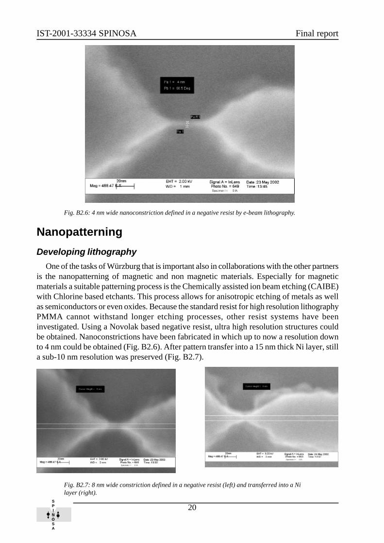
Fig. B2.6: 4 nm wide nanoconstriction defined in a negative resist by e-beam lithography.
Fig. B2.7: 8 nm wide constriction defined in a negative resist (left) and transferred into a Nilayer (right).
Nanopatterning
Developing lithography
One of the tasks of Würzburg that is important also in collaborations with the other partnersis the nanopatterning of magnetic and non magnetic materials. Especially for magneticmaterials a suitable patterning process is the Chemically assisted ion beam etching (CAIBE)with Chlorine based etchants. This process allows for anisotropic etching of metals as wellas semiconductors or even oxides. Because the standard resist for high resolution lithographyPMMA cannot withstand longer etching processes, other resist systems have beeninvestigated. Using a Novolak based negative resist, ultra high resolution structures couldbe obtained. Nanoconstrictions have been fabricated in which up to now a resolution downto 4 nm could be obtained (Fig. B2.6). After pattern transfer into a 15 nm thick Ni layer, stilla sub-10 nm resolution was preserved (Fig. B2.7).
IST-2001-33334 SPINOSA Year 1 Part2: Work progress overview
21SPINOSA
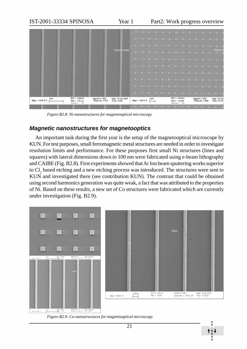
Magnetic nanostructures for magnetooptics
An important task during the first year is the setup of the magnetooptical microscope byKUN. For test purposes, small ferromagnetic metal structures are needed in order to investigateresolution limits and performance. For these purposes first small Ni structures (lines andsquares) with lateral dimensions down to 100 nm were fabricated using e-beam lithographyand CAIBE (Fig. B2.8). First experiments showed that Ar Ion beam sputtering works superiorto Cl2 based etching and a new etching process was introduced. The structures were sent toKUN and investigated there (see contribution KUN). The contrast that could be obtainedusing second harmonics generation was quite weak, a fact that was attributed to the propertiesof Ni. Based on these results, a new set of Co structures were fabricated which are currentlyunder investigation (Fig. B2.9).
Figure B2.8: Ni-nanostructures for magnetooptical microscopy
Figure B2.9: Co-nanostructures for magnetooptical microscopy
IST-2001-33334 SPINOSA Final report
22SPINOSA
Ni 50nm
Ni 30 nm
Au 100nm
Al 5nm
TI
SiSiO2
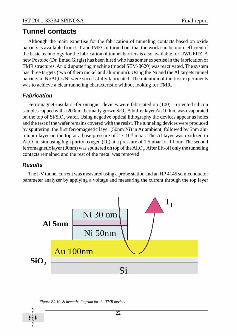
Figure B2.10. Schematic diagram for the TMR device.
Tunnel contactsAlthough the main expertise for the fabrication of tunneling contacts based on oxide
barriers is available from UT and IMEC it turned out that the work can be more efficient ifthe basic technology for the fabrication of tunnel barriers is also available for UWUERZ. Anew Postdoc (Dr. Emad Girgis) has been hired who has somer expertise in the fabrication ofTMR structures. An old sputtering machine (model SEM-8620) was reactivated. The systemhas three targets (two of them nickel and aluminum). Using the Ni and the Al targets tunnelbarriers in Ni/Al2O3/Ni were successfully fabricated. The intention of the first experimentswas to achieve a clear tunneling characteristic without looking for TMR.
Fabrication
Ferromagnet-insulator-ferromagnet devices were fabricated on (100) – oriented siliconsamples capped with a 200nm thermally grown SiO2. A buffer layer Au 100nm was evaporatedon the top of Si/SiO2 wafer. Using negative optical lithography the devices appear as holesand the rest of the wafer remains covered with the resist. The tunneling devices were producedby sputtering the first ferromagnetic layer (50nm Ni) in Ar ambient, followed by 5nm alu-minum layer on the top at a base pressure of 2 x 10⁻² mbar. The Al layer was oxidized toAl2O3 in situ using high purity oxygen (O2) at a pressure of 1.5mbar for 1 hour. The secondferromagnetic layer (30nm) was sputtered on top of the Al2O3. After lift-off only the tunnelingcontacts remained and the rest of the metal was removed.
Results
The I-V tunnel current was measured using a probe station and an HP 4145 semiconductorparameter analyzer by applying a voltage and measuring the current through the top layer

IST-2001-33334 SPINOSA Year 1 Part2: Work progress overview
23SPINOSA
Figure B2.11. The TMR devices (circular shape) on the top of buffer layer 100nm Au.
NiAu100µm2
-0,3 -0,2 -0,1 0,0 0,1 0,2 0,3-0,004
-0,003
-0,002
-0,001
0,000
0,001
0,002
0,003
0,004
Different Tunnel Junctions from Al2O3
Voltage (V)
96
97
98
99
100
101
102
103
104
-0,4 -0,2 0,0 0,2 0,4
-0,020
-0,015
-0,010
-0,005
0,000
0,005
0,010
0,015
0,020
20,8
21,0
21,2
21,4
21,6
21,8
22,0
-0,6 -0,4 -0,2 0,0 0,2 0,4 0,6
-0,045
-0,036
-0,027
-0,018
-0,009
0,000
0,009
0,018
0,027
0,036
0,045
Res
ista
nce
(Ω)
Res
ista
nce
(Ω)
Cur
rent
(A
)
Voltage (V)
12,2
12,3
12,4
12,5
12,6
12,7
12,8
12,9
13,0
13,1
-0,6 -0,4 -0,2 0,0 0,2 0,4 0,6-0,015
-0,010
-0,005
0,000
0,005
0,010
0,015
Cur
rent
(A)
46
47
48
49
50
51
52
53
54
Figure B2.12. The I-V curve and the resistance device for Ni/Al2O3/Ni.
(Ni) and the bottom layer (Au). Figure B2.10. shows the schematic diagram for the wholesystems, with the multilayer structure. The arrow shows the tunnel current direction.
Figure B2.11. shows an optical picture of the tunneling contacts (circular shape) withdifferent dimensions on the top of the Au layer. Figure B2.12. shows typical I-V (tunnel)traces and the device resistance of different Ni/Al2O3/Ni structures .
Before the preparation of tunneling contacts on semiconductor devices in order to get acloser look at the spin injection mechanism between TMR devices and the semiconductor,

IST-2001-33334 SPINOSA Final report
24SPINOSA
the group of UWUERZ will optimize the fabrication of TMR devices and the interfacesbetween the TMR devices and the semiconductor materials. This work will be done in closecollaboration with IMEC and UT, where this technology is available in high quality. Thenext steps in this direction are the preparation of TMR devices with different ferromagneticmaterials and the optimization of the barrier by preparing a very thin barrier (without pinholes)using different oxidation methods (UV assisted oxidation , natural, and thermal oxidation)and also optimization of the metal/insulator/semiconductor interfaces.

IST-2001-33334 SPINOSA Year 1 Part2: Work progress overview
25SPINOSA
KUN
IntroductionThe Nijmegen group was not directly involved in the deliverables set for year 1 of the
project. 1st year’s work was mostly dedicated to set up the measurement tools for thecharacterization of samples based on the technologies developed by other groups duringyear 1. During the remaining time of the project, time and spin resolved optical studies willbe carried out on spin injection samples fabricated by other partners.
The main goals for year 1 were:
- to set up a ”permanent” scheme for magneto-optical pump-probe measurements
- to acquire and set up a combined linear and nonlinear magneto-optical microscope
- to learn the measurements of spin dynamics in semiconductors
- to analyse the possibility of magneto-optical detection of the magnetic properties ofnanocontacts
The efforts taken to achieve these goals and the results obtained will be described in thefollowing.
Pump-probe measurements
Semiconductors
The technique to study the ultrafast carrier and spin dynamics at room temperature basedon the measurements of the photo-induced magneto-optical Kerr effect was developed andapplied earlier for bulk semiconductors (GaAs, heavily n-doped GaAs and CdTe) andsemiconductor heterostructures (AlGaAs/GaAs). Several contributions to the Kerr effectwere observed. It was found that the contributions are characterised by different kinds ofspectral behaviour that dominate in different time domains. The theoretical analysis of theresults was done and allowed to extract from the data the time of the energy relaxation ofelectrons in the conduction band, the time of exciton ionisation and time of spin relaxationin the studied semiconductors at room temperature.
The knowledge of the spin lifetime in semiconductors is an important parameter, which isnecessary for the design of the novel spintronics devices. Beyond the GHz frequency domain,the spin dynamics can only be studied by optical techniques such as polarizedphotoluminescence or magneto-optical effects. Both magneto-optical Faraday effect in thetransmission geometry and Kerr effect in the reflection geometry are well suited for studiesof the spin dynamics in a broad spectral – including wavelengths where no luminescencecan be measured - as well as thermal range.
The goal of the following study was the observation and understanding of picosecondand sub-picosecond dynamics of electron and hole spins in intrinsic and p-doped InP in thebroad temperature range from 20 K up to 300 K.

IST-2001-33334 SPINOSA Final report
26SPINOSA
The study was done using the time-resolved, pump and probe, photo-induced magneto-optical Kerr effect. For the experiments a pulsed Ti:sapphire laser was used with a pulseduration of approximately 100 fs and a repetition rate of 82 MHz. The measurements weredone in the spectral range from 1.47 eV to 1.57 eV nearby the transition between the split-off valence band and the conduction band (Eg=1.53 eV). The Kerr rotation and ellipticity
Figure B3.1. Time dependence of the MOKE rotation induced in InP sample measured withpump-probe technique. Three relaxation processes with decay times of 10 ps, 20 ps and 300 pscan be distinguished.
Figure B3.2. Spectral dependence of three different relaxation processes characterized byrelaxation times of 10 ps (a), 20 ps (b), and 300 ps (c). Both MOKE rotation and ellipticity areplotted.
0.0
-0.2
-0.4
-0.6
-0.8
-1.0
-1.2
-1.4
-20 0 20 40 60 80 100 120 140
Kerr
rota
tion
(mra
dcm
2G
W-1)
Time delay (ps)
hν=1.53 eVInP20 K
Three relaxation processes with decay times
Kerr
effe
ct(m
rad
cm2G
W-1)
1.46 1.48 1.50 1.52 1.54 1.56 1.58
-0.4
-0.2
0.0
0.2
0.4
0.6
0.8
1.0
ellipticity
Photon energy (eV)
Eg
Component with τ =10 ps
InP20 K
rotation
1.48 1.50 1.52 1.54 1.56
-1.2
-0.9
-0.6
-0.3
0.0
0.3
0.6
0.9
1.2
Eg
InP20 K
Component with τ =20 ps
Photon energy (eV)1.48 1.50 1.52 1.54 1.56
-1.6
-1.2
-0.8
-0.4
0.0
0.4
0.8
1.2
1.6
2.0
2.4
Eg
InP20 K
Component with τ >300 ps
Photon energy (eV)
a) b) c)

IST-2001-33334 SPINOSA Year 1 Part2: Work progress overview
27SPINOSA
experienced by the reflected delayed probe pulses were measured as a function of the timedelay between pump and probe pulses.
The typical temporal behaviour of the photoinduced Kerr rotation is shown in FigureB3.1. Three relaxing components with decay times of about 10 ps, 20 ps and more than 300ps can be distinguished in the magneto-optical signal. The spectral behaviour of thesecomponents was analysed. Based on the obtained spectra, theoretical predictions andsimulations, the component with a decay time of 10 ps (Fig. B3.2) has turned out not to berelevant for spin dependent phenomena but rather caused by phase space filling effects.
The component with decay time 20 ps and more than 300 ps (Figure B3.2) had similarspectral behaviour and were shown to be caused by the splitting of the spin sublevels. Theorigin of the component with decay time 20 ps has not been revealed yet. The longestrelaxation time is connected to the electron spin relaxation in the conduction band. Thetemperature behaviour of the spin relaxation time is shown in Figure B3.3 together with thefit according to the D’yakonov-Perel mechanism.
The results of this study will be presented at a conference on: ”Nonlinear Optics &Excitation Kinetics in Semiconductors: 7th Internat. Workshop (NOEKS 2003)”, held from24-28 February 2003 in Karlsruhe, Germany
Figure B3.3. Temperature dependence of the long-living excitation relaxation time.
100 200 30010
100
1000
Elec
tron
spin
rela
xatio
n(p
s)
Temperature (K)
T-3
InP
M. I. D'yakonov et al

IST-2001-33334 SPINOSA Final report
28SPINOSA
Dielectrics
With the help of the same technique the temporally and spectrally resolved study of thenonlinear optical properties of Mn3+ magnetic ions in rare earth manganites YMnO3, ErMnO3and ScMnO3 was done. It was found that nonlinear optical contributions to off-diagonalelements of the dielectric permittivity tensor decay faster than 50 fs, while the contributionto the diagonal elements are present during a much longer time – more than 70 ps afterexcitation. The spectral peculiarities of the observed phenomena were analysed andmechanisms of the relaxation processes based on the electron and phonon dynamics wereproposed for the fast and long relaxation processes, respectively.
The time-resolved study of the photo-induced phase transition from the antiferromagneticto the paramagnetic phase was done in FeBO3. It was shown that after excitation of theFeBO3 by 100 fs laser pulses the crystal looses its magnetic order within 700 ps, which is 20times faster than the typical spin-lattice relaxation time in FeBO3 obtained by measurementsof ferromagnetic resonance. Such kind of acceleration is due to a non-equilibrium phonondistribution caused by the optical excitation. These results are published in Physical ReviewLetters.
Figure B3.4 The short term transient Faraday rotation, (b) the intensity dependence of theultrafast Faraday rotation solid lines, and (c) the long term transient Faraday rotationmeasured for different bias temperatures. The antiferromagnetic order is destroyed at a timedelay of 500 ps and 200 ps for Tbias=346.5 K and Tbias=346.8 K, respectively. The solid linesare guides to the eye.
Fara
day
rota
tion
(mra
d)
Time delay (ps)
(a)
(b)
Time delay (ps)
Mea
sure
d M
O s
igna
l (m
V)
Fara
day
rota
tion
(mra
d)
Pump fluence (mJ cm )-2
step
(c)

IST-2001-33334 SPINOSA Year 1 Part2: Work progress overview
29SPINOSA
Magneto-optical microscopeInstallation and design of a combined linear and nonlinear high-resolution magneto-optical
microscope. This microscope is based on a commercial inverted microscope Leica IRM thatwas upgraded, both optically and magnetically, to allow an easy and fast observation ofmagnetic domains in both polar and longitudinal magnetic geometries.
Figure B3.5 Faraday effect at negative (solid circles) and at zero (open circles) time delay as afunction of the bias temperature. The difference between magnetooptical signal at -20 ps and500 ps is shown by diamonds and the dashed line is a calculation. The inset shows the transientcomponent of the magnon temperature as a function of the time delay.
Figure B3.6 The new magneto-optical microscope
αF(
0 ps
), α
F(-2
0 ps
) (m
rad)
αF(
-20
ps) -
(m
rad)
αF(
500
ps) ∆
T(t)
, KS
Bias temperature (K)
Time delay (ns)
2.4
2.0
1.6
1.2
0.8
0.4
0
12
2
350
1.50
0.75
0
0 1 2

IST-2001-33334 SPINOSA Final report
30SPINOSA
Figure B3.7 Written bits on the recordable CD
The far-field resolution of this microscope allows one to easily observe magnetic lineswith 300 nm period. In the following, the microscope will be adapted (i) to allow automaticscanning necessary for the MSHG imaging, and (ii) also to allow the use of a Solid Immers-ion Lens for further resolution enhancement.
To test the operation as well as the resolution of the microscope, we used a piece of arecordable CD (see Figure B3.7). Written bits were easily visualized.
Study of magnetization in nanostructures by magneto-optical diffraction and microscopy.
Pt/CoNi/Pt samples from Twente
The fact, that in most cases magnetic nanostructures are used in the form of periodicarrays, calls for the use of magneto-optical diffraction for their investigation. In addition tostandard linear optical diffraction (including the measurement of magneto-optical effects),

IST-2001-33334 SPINOSA Year 1 Part2: Work progress overview
31SPINOSA
also MSHG diffraction could be useful providing information over the surfaces, interfaces,and probably also the edges of such structures.
Figure B3.8 shows SEM images of two samples used for the initial tests. Pt/CoNi/Ptlayers (obtained from University of Twente) were lithographically patterned to a 5 mm period(sample 1) and to a 300 nm period (sample 2).
For the measurements, a pulsed laser beam from a Ti–sapphire laser (76 MHzX100 fspulses) with a wavelength of 760 or 810 nm was focussed onto the sample. The polarizationof the incoming fundamental laser beam could be chosen using a Babinet Soleil compensatorand a polarizer was used afterwards to ensure a high degree of light polarization. An analyzerwas set to choose the polarization of the outgoing SHG, that was detected after proper filteringwith a photomultiplier.For the MOKE hysteresis measurements, a Wollaston prism incombination with a differential 2-diode detection scheme was employed. The angle ofincidence was always 45o, while the detection arm could be rotated in order to measure the
Figure B3.8. SEM images of the periodically structured samples.
Figure B3.9. The experimental setup used for the diffraction measurements.
detector(s)
various inputpolarizations
Magnetic field:transversegeometry
800 nm, 100 fs

IST-2001-33334 SPINOSA Final report
32SPINOSA
magneto-optical signal as a function of the diffraction angle (Figure B3.9). The transversalmagneto-optical geometry was used for all experiments.
Figure B3.10 shows hysteresis loops measured in different diffraction orders for the samplewith d=5 mm. In this configuration (combination of angle of incidence, wavelength andstructure period) only the 1st order linear diffraction could be seen. On the other hand, several
Figure B3.10. MOKE hysteresis loops measured in different diffraction orders for sample 1.
Figure B3.11. MOKE and MSHG hysteresis loops measured with 405 nm and 810 nmwavelengths from sample 2.
-200 -100 0 100 200
-200 -100 0 100 200 -200 -100 0 100 200
Magnetic field (Oe)
1 orderst
0 orderth
-1 orderst
-2 ordernd
-3 orderrd
-600 -300 0 300 600
Magnetic field (Oe)
-600 -300 0 300 600
Magnetic field (Oe)
0 orderMOKE
th
0 orderMSHG
th
-1 orderMOKE(405 nm)
st
-1 orderMSHG(810 nm)
st

IST-2001-33334 SPINOSA Year 1 Part2: Work progress overview
33SPINOSA
diffracted orders were observed at negative angles. For the sample with period d=0.3 mm(see Figure B3.11) only the –1st order MSHG diffraction could be observed at the funda-mental wavelength of 810 nm. To measure the MOKE hysteresis loops in the same direction,a blue GaN laser with l=405 nm was used.
Figure B3.12 presents the dependence of the MSHG intensity for two opposite magneticdirections as a function of the detection angle. Obviously the MSHG signal is limited tonarrow diffraction peaks. The background is practically equal to the dark current of thephotomultiplier. This means the absence of any large-scale roughness that may cause strongdiffusive SHG.
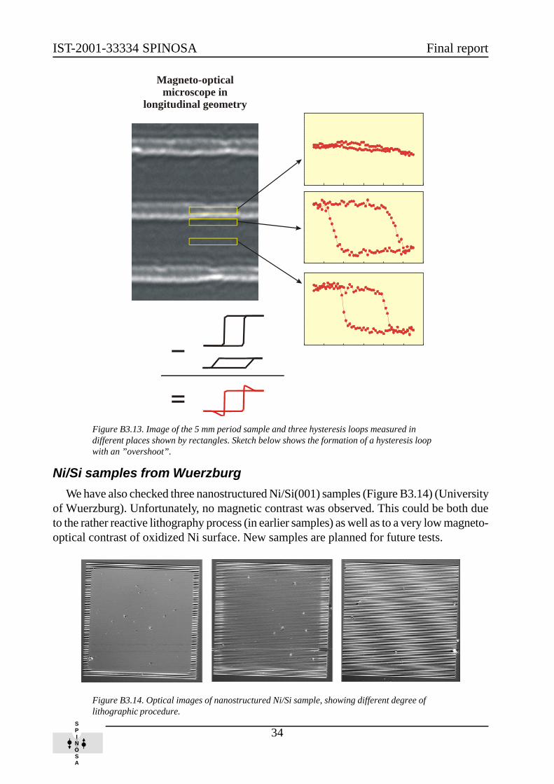
The shape of the first-order diffraction hysteresis loops differs from all others by showingan ”overshoot” at the magnetization reversal (see Fig. B3.10). Such an overshoot has alreadybeen observed before in linear MOKE and can tentatively be explained by an inhomogeneousreversal of the magnetization in the stripes. It is reasonable to suppose that, due to thelithography process, the edges of a stripe have a higher density of defects and therefore alarger coercive field Hc, due to the pinning. To confirm this assumption, we performedmagneto-optical microscopy experiments that allowed us to measure the magnetizationhysteresis loops selectively from different places on the sample (see Figure B3.13). Thedifference in coercive fields was thus unambiguously demonstrated.
Figure B3.12. Dependence of the MSHG intensity for two opposite magnetic direction as afunction of the detection angle.
+M −M
MSH
G in
tens
ity (c
ount
s/se
c)
1
10
100
1000
Diffraction angle (deg)0 5 10 15-5-10
IST-2001-33334 SPINOSA Final report
34SPINOSA
Figure B3.13. Image of the 5 mm period sample and three hysteresis loops measured indifferent places shown by rectangles. Sketch below shows the formation of a hysteresis loopwith an ”overshoot”.
Ni/Si samples from Wuerzburg
We have also checked three nanostructured Ni/Si(001) samples (Figure B3.14) (Universityof Wuerzburg). Unfortunately, no magnetic contrast was observed. This could be both dueto the rather reactive lithography process (in earlier samples) as well as to a very low magneto-optical contrast of oxidized Ni surface. New samples are planned for future tests.
Figure B3.14. Optical images of nanostructured Ni/Si sample, showing different degree oflithographic procedure.
Magneto-opticalmicroscope in
longitudinal geometry

IST-2001-33334 SPINOSA Year 1 Part2: Work progress overview
35SPINOSA
Personnel and plansWe have hired two postdocs (Dr. A.V. Kimel from the end of May and Dr. A.A Tsvetkov
from October 1st) to work on the SPINOSA project.
A new setup for ultra-sensitive measurements of magneto-optical Kerr effect insemiconductors is being built. Two semiconductor samples were obtained from Wuerzburgwith the aim to detect the spin polarization in semiconductor magneto-optically.
New samples are planned in order to continue the experimental work on the detection ofthe magnetization of nanocontacts. Various structure geometries are being discussed.
Several magnetite samples are obtained from Bologna, for magneto-opticalcharacterization, including microscopy.

IST-2001-33334 SPINOSA Final report
36SPINOSA

IST-2001-33334 SPINOSA Year 1 Part2: Work progress overview
37SPINOSA
UT
IntroductionAlready in year 1 UT was involved in WP 1 and WP 2. In Wp1 the work was mainly
dedicated to the preparation for deliverable D7(month 24):
Demonstration of injection of highly spin polarized hot electrons into a semiconductor at lowtemperature, low field control of the polarization.
This is described below.
Hot electron spin-filtersOne of the aims in WP 1 is to use hot-electron spin filtering in standard ferromagnetic
materials for spin-injection into semiconductors. In this approach we use a three-terminaldevice structure with a hot-electron emitter, a ferromagnetic base metal and a semiconductorcollector. The ferromagnetic base acts as a spin-filter for hot electrons. A first step towardachieving the goal is to determine the transmission of such a spin filter and to quantify theresulting spin polarization of the transmitted hot electrons. To do this, we have used transportstudies in the spin-valve transistor geometry, with traditional ferromagnetic materials such
Fig.B4.1. Hot-electron spin-filter properties of a Co or NiFe thin film, as calculated fromexperimentally determined scattering lengths for hot electrons at 0.9 eV. Top left panel:resulting spin-polarization at 100 K after the hot-electron beam has passed through the film.Bottom left panel: total transmitted fraction of hot electrons (at 100 K and 300 K). Right panel:spin-filter polarization versus temperature for a 6 nm NiFe film.

IST-2001-33334 SPINOSA Final report
38SPINOSA
as Co and NiFe. These are materials with low coercivity and high Curie temperature, whichin principle allow room temperature operation. Experiments have shown that such thin filmsacts as highly efficient spin-filter for hot electrons, with polarization rapidly approaching100% for films of only a few nanometer thick. Quantitative data on the spin-polarizationand overall transmission are shown in fig.B4.1. Note that these data are for a hot-electroncurrent that has been filtered by a thin ferromagnetic film, i.e. the parameters may stillchange when this current is subsequently injected into a semiconductor.
We find that for Co as well as for NiFe, a hot-electron spin-polarization above 90% isobtained for films of only 4 nm thick. The corresponding total transmission for NiFe isaround 0.1, which would facilitate a reasonable current density for injection into thesemiconductor. The transmission for Co is somewhat smaller, due to the shorter scatteringlength for majority spin hot electrons in Co as compared to NiFe. The data also show thatthere is a slight reduction in transmission as well as hot-electron spin-polarization withincreasing temperature, which is primarily due to excitation of spin waves. However, theeffect was found to be weak, and highly spin-polarized hot electrons are still obtained atroom temperature. Based on this data, we have selected NiFe as the most promising materialfor the achieving the deliverable D7 in month 24.
Together with partner IMEC, we have started designing test transistor structures thatcombine a hot-electron spin filter with a collector that contains a GaAs based LED fordetection of the injected spin-polarization. Two options for the hot electron emitter structureare considered, a Schottky contact or a tunneling contact. This requires deposition of diffe-rent kinds of materials as well as the possibility to create Aluminum oxide tunnel barriers.The necessary modifications to an existing UHV deposition system have been implementedand tested, and it is now fully operational for the project to fabricate the variety of structuresas mentioned under section 9.3.1.1 of the work package 1 description.

IST-2001-33334 SPINOSA Year 1 Part2: Work progress overview
39SPINOSA
UOXF.DK
IntroductionDuring the first 12 months of the EC project SPINOSA, the Oxford Group concentrated
on WP1.3 – the experimental investigation of tunnelling magnetoresistance (TMR) inferromagnetic nanoparticles with a silicon Schottky barrier. A publication is in preparationon this work and as a result of the initial measurements, a sample composed of Si/SiO2(3nm)/Co(6nm)/Al(20nm) was given to the Nijmegen group in order to investigate the magnetisationdynamics using MSHG. This report will give an overview of the sample fabrication, expe-rimental results, and the proposed physical model for these anomalous results.
Sample FabricationThe samples were fabricated as follows.
1) A silicon-on-insulator (SOI) wafer (205nm of device quality Si on top of 400nm ofsilicon dioxide) was covered with UV resist.
2) Several regions were defined using UV lithography.
3) These regions were then selectively doped. The five different wafers in the processhad four doping configurations: (n-type and p-type 1016 and 1018 atoms/cm3 respectively).
4) The UV resist was removed.
5) Co was deposited over the whole wafer using magnetron sputtering.
6) Co pads were defined by UV lithography and etching.
7) The remaining resist was removed and the samples were scribed and inspected underthe microscope.
Although the optical quality of the devices was good, initial electrical inspection indicatedthat there was a conducting surface layer on the samples. This parasitic conducting layer
Figure B5.1 - Schematic of the final Co-Si structure

IST-2001-33334 SPINOSA Final report
40SPINOSA
was a thin film of cobalt silicide which had formed during the deposition of cobalt onto thesilicon and which the cobalt etchant had not successfully removed. The existence of cobaltsilicide was confirmed by MULSAM microscopic surface analysis (using Auger and X-rayscan) at the University of York. This layer covered the entire wafer including the devices,making transport measurements difficult to interpret. The solution to this problem was toion-mill the samples using a 3 cm-diameter Kaufmann source for just long enough to removethe silicide without appreciably eating into the 200nm doped silicon beneath. Figure B5.1shows a schematic of the final structure.
Experimental Methods and ResultsThe differential resistance of the Co/Si/Co devices was measured by an AC four-point
method. A current of 0.4mA at 113Hz was applied and the voltage drop across the Co/Si/Costructure was followed by a lock-in amplifier. The samples were cooled in a continuous flowHe cryostat to an initial temperature of 4K. The resistance was measured as a function ofapplied magnetic field from 0 to 1.5T. The temperature was increased and the measurementsrepeated, at a range of temperatures until 25 K. A sample IV curve is shown in Figure B5.2and the magnetoresistance (MR) curves are shown in Figure B5.3. In addition, the resistancechange of the samples was measured when exposed to incident HeNe laser light (see FigureB5.4). The samples exhibited an anomalous photo-effect since the resistance actually increasedwith incident light intensity. This change in the resistance was 20% and remainedapproximately constant in the temperature regime considered.
Figure B5.2 - Current-voltage characteristics of Co/Si(1µm)/Co on Sample 40903 at 150-200 K.

IST-2001-33334 SPINOSA Year 1 Part2: Work progress overview
41SPINOSA
DiscussionSeveral unexplained results arose from the measurements on the lateral Co-Si structures
including 20% MR at temperatures less than 23K and the anomalous photo-effect. A modelbased on a two-dimensional granular lattice of small Co particles (see Figure B5.5) dispersedrandomly on the surface of insulating Si is used to explain these results. This 2D lattice issimilar to that observed by E. Gu et. al [E. Gu, S. Hope, M. Tselepi, and J.A.C. Bland, Phys.Rev. B 60(6) 4092 (1999)] during ultrathin film growth of Co on Cu(110). This finding waslater confirmed with scanning electron microscopy; Traces of granular material appear inthe gap region, but the average size and size distribution of the granules is difficult to quantify.
The first step in the model was to relate the observed change in the resistance of thesystem under the applied magnetic field with the change in the overall magnetisation. Since
Figure B5.3 – AC magnetoresistance curves of Co/Si(16µm)/Co on Sample 41105 from 4 to25K; The current of 0.4mA at 113Hz is parallel to the field.
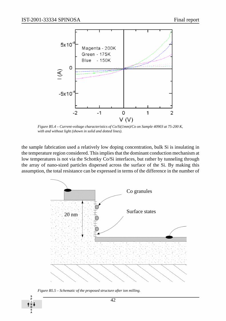
IST-2001-33334 SPINOSA Final report
42SPINOSA
Figure B5.4 – Current-voltage characteristics of Co/Si(1mm)/Co on Sample 40903 at 75-200 K,with and without light (shown in solid and dotted lines).
the sample fabrication used a relatively low doping concentration, bulk Si is insulating inthe temperature region considered. This implies that the dominant conduction mechanism atlow temperatures is not via the Schottky Co/Si interfaces, but rather by tunneling throughthe array of nano-sized particles dispersed across the surface of the Si. By making thisassumption, the total resistance can be expressed in terms of the difference in the number of
Figure B5.5 – Schematic of the proposed structure after ion milling.
20 nm
Co granules
Surface states