Embed Size (px)
Citation preview

FieldEffectTransistors
Lecture9

38
Types of FET
• Metal Oxide Semiconductor Field Effect Transistor – MOSFET – Enhancement mode – Depletion mode
• Junction FETs • p channel vs n channel

39
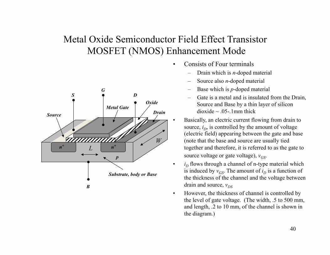
Metal Oxide Semiconductor Field Effect Transistor MOSFET (NMOS) Enhancement Mode
• Consists of Four terminals – Drain which is n-doped material – Source also n-doped material – Base which is p-doped material – Gate is a metal and is insulated from the Drain,
Source and Base by a thin layer of silicon dioxide ~ .05-.1mm thick
• Basically, an electric current flowing from drain to source, iD, is controlled by the amount of voltage (electric field) appearing between the gate and base (note that the base and source are usually tied together and therefore, it is referred to as the gate to source voltage or gate voltage), vGS.
• iD flows through a channel of n-type material which is induced by vGS. The amount of iD is a function of the thickness of the channel and the voltage between drain and source, vDS
• However, the thickness of channel is controlled by the level of gate voltage. (The width, .5 to 500 mm, and length, .2 to 10 mm, of the channel is shown in the diagram.)
p
n+ n+
S G
D
B
Substrate, body or Base
Drain
Oxide Metal Gate
Source
40
Metal Oxide Semiconductor Field Effect Transistor MOSFET (NMOS) Enhancement Mode
p
n+ n+
S G
D
B
Substrate, body or Base
Drain
Oxide Metal Gate
Source
• Consists of Four terminals – Drain which is n-doped material – Source also n-doped material – Base which is p-doped material – Gate is a metal and is insulated from the Drain,
Source and Base by a thin layer of silicon dioxide ~ .05-.1mm thick
• Basically, an electric current flowing from drain to source, iD, is controlled by the amount of voltage (electric field) appearing between the gate and base (note that the base and source are usually tied together and therefore, it is referred to as the gate to source voltage or gate voltage), vGS.
• iD flows through a channel of n-type material which is induced by vGS. The amount of iD is a function of the thickness of the channel and the voltage between drain and source, vDS
• However, the thickness of channel is controlled by the level of gate voltage. (The width, .5 to 500 mm, and length, .2 to 10 mm, of the channel is shown in the diagram.)
L W
41
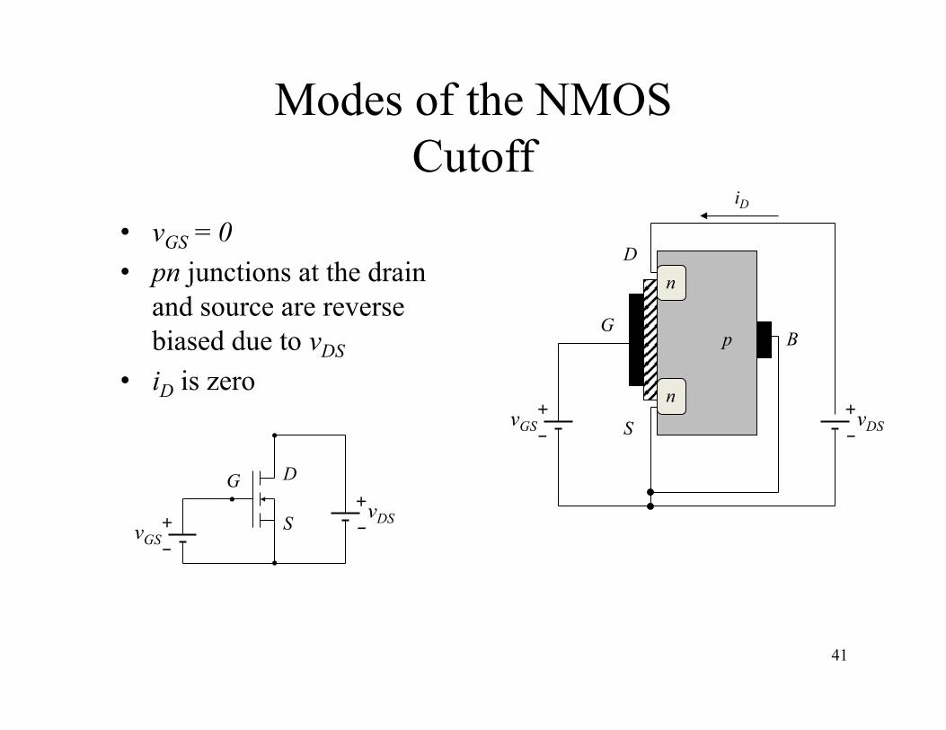
Modes of the NMOS Cutoff
• vGS = 0 • pn junctions at the drain
and source are reverse biased due to vDS
• iD is zero
n
n
p
S
B G
D
+
-vGS
+
-vDS
iD
+
-vGS
+
-vDS S
D G

42
Modes of the NMOS Triode Region
• vGS ≥ Vto a threshold voltage which causes electrons in the base to be attracted to and holes to be repelled from the region just below the gate
• This process causes a n-type channel to form below the gate
• As vDS is increased, iD starts to flow. For small values of vDS, iD is proportional to vDS
• In addition, iD is proportional to vGS- Vto, the excess gate voltage
• Therefore, the MOSFET can act as a voltage controlled resistor in the Triode Region (e.g., used in AGC circuits)
n
n
p
S
B G
D
+
-vGS
+
-vDS
iD
vDS
iD increasing vGS

43
Modes of the NMOS Triode Region
n
n
p
S
B G
D
+
-vGS
+
-vDS
iD
vDS
iD increasing vGS
• vGS ≥ Vto a threshold voltage which causes electrons in the base to be attracted to and holes to be repelled from the region just below the gate
• This process causes a n-type channel to form below the gate
• As vDS is increased, iD starts to flow. For small values of vDS, iD is proportional to vDS
• In addition, iD is proportional to vGS- Vto, the excess gate voltage
• Therefore, the MOSFET can act as a voltage controlled resistor in the Triode Region (e.g., used in AGC circuits)

44
Modes of the NMOS Triode Region (Continued)
• Since the drain is more positive than the source, the voltage difference between the channel and the gate varies along the channel from drain to source.
• As vDS is further increased, this channel voltage profile causes a tapering of the channel thickness. vGD ≠ vGS
• This tapering causes the resistance of the channel to increase (as vDS increases) and, thereby, reduces the rate of increase of iD.
• Furthermore, it can be shown that
• To summarize: vGS ≥ Vto and vDS< vGS-Vto
p
S
B G
D
+
-vGS
+
-vDS
iD
n
)2)(()2)((
])(2[ 2
oxn
DSDStoGSD
CLWKP
LWK
vvVvKiµ==
−−=
vDS
iD increasing vGS
n

45
Modes of the NMOS Saturation
• As vDS continues to increase, the voltage profile continues to taper. When the gate to channel voltage at the drain, vGD, approaches Vto , the thickness of the channel at the drain is (virtually) zero. (Note that although the channel thickness is virtually zero, current flow is not cutoff since it is needed to support the channel voltage profile.)
• This phenomenon limits the amount of drain current (i.e., iD is saturated) and causes iD to be independent of vDS
• Furthermore, it can be shown that
• Summarize: vGS ≥ Vto and vDS ≥ vGS- Vto
n
p
S
B G
D
+
-vGS
+
-vDS
iD
n
2)( toGSD VvKi −=
vDS
iD Saturation
Triode
46
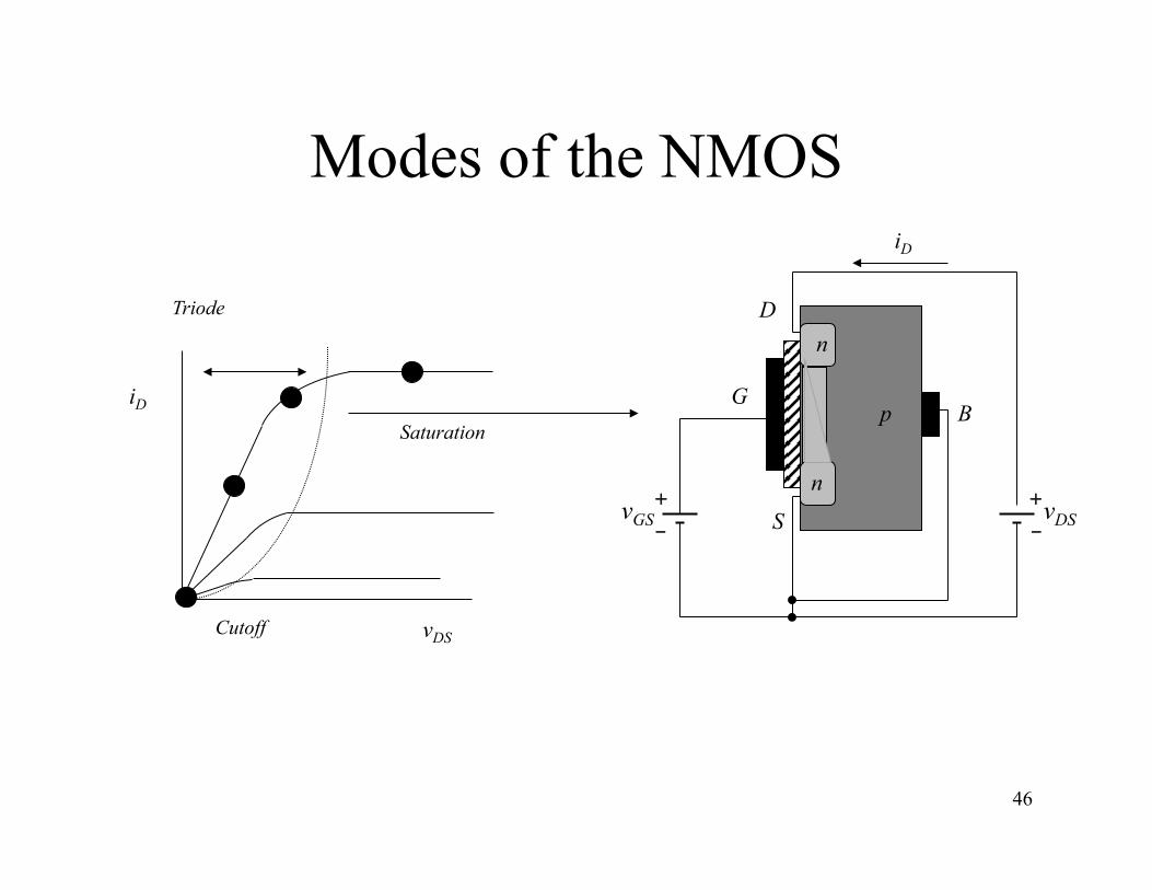
Modes of the NMOS
p
S
B G
D
+
-vGS
+
-vDS
iD
n
n
vDS
iD
Saturation
Triode
Cutoff

47
NMOS Characteristics
Note that for NMOS devices with short channel lengths, a tilt may exist due to the modulation of the channel length by the depletion region surrounding the drain.
0
5
10
15
20
0 2 4 6 8 10 12 14 16 18 20
vDS Volts
iD mA vGS = 5v
vGS = 4v
vGS = 3v
vGS = 2v Note that Vto = 1

0
5
10
15
20
0 2 4 6 8 10 12 14 16 18 20
iD mA
vDS Volts
vGS = 5v
vGS = 4v
vGS = 3v
vGS = 2v
48
Load Line of a NMOS Amplifier
sin(2000πt)
Gate Circuit( )
sin(2000 ) 4
Drain Circuit
20 1000
GS in
D DS
D DS
v v t VGGt
VDD i RD vi v
π= += +
= += +
4 11 16
Inverted and distorted
M1Mname
Vin+-
VGG
4V+ -
RD1k
VDD20V
+
-
0
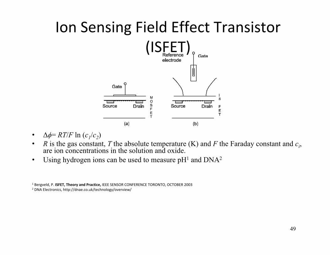
IonSensingFieldEffectTransistor(ISFET)
• Δϕ= RT/F ln (c1/c2) • R is the gas constant, T the absolute temperature (K) and F the Faraday constant and ci,
are ion concentrations in the solution and oxide. • Using hydrogen ions can be used to measure pH1 and DNA2
1Bergveld,P.ISFET,TheoryandPractice,IEEESENSORCONFERENCETORONTO,OCTOBER20032DNAElectronics,http://dnae.co.uk/technology/overview/
49

50
n-channel Junction FET
Gate
Drain
pp
Source
n
S
D
G

51
N-channel JFET Gate Bias
G
D
n
pp
S
0>vGS>Vto
Small bias results in larger depletion layer and smaller channel
G
D n
pp
S
+
-
vGS≤Vto
Larger bias > pinch-off voltage, Vto, creates overlapping depletion layer and no conductive path from drain to source
Cutoff Region
Zero Bias and depletion layer is thin and conduction channel exists from drain to source
G
D
n
pp
S
+
-

52
n-channel JFET Operation
G
D n
pp
S
+
-G
D n
pp
S
+
-
With vGS=0, we increase vDS and enter the Triode Region. As a result ID increases and is proportional to vDS. As vDS increases further, the depletion region between drain and gate grows (with a larger area nearer the drain) and adds more resistance in the channel by narrowing its width. Thus, the rate of drain current increase slows down with increasing vDS. As vDS reaches the pinch-off voltage, Vt0, the drain current, ID saturates (i.e., the FET is in the Saturation Region).
vDS
iD Saturation
Triode
vDS≤ |Vto| vDS> |Vto|
Triode Region Saturation Region
With vGS<0, the same phenomenon occurs as vDS is increased. However, the non-zero value of vGS increases the resistance in the channel due to a large depletion layer and therefore, values of ID are smaller both in the Triode and Saturation regions.
G
D
n
pp
S
+
-
vDS= 0
ID=0

53
n-channel JFET Operation
G
D
n
pp
S
+
-
vDS= 0
As vDS increase ID increases and JFET enters the Triode Region.
vDS
iD Saturation
Triode
Cutoff

54
n-channel JFET Operation
G
D
n
pp
S
+
-
vDS= 0
vDS
iD Saturation
Triode
Cutoff
Triode Region Because the channel is “wide”, ID is proportional to vDS.

55
n-channel JFET Operation
G
D n
pp
S
+
-
vDS≤ |Vto|
Triode Region While vDS increases, the depletion region also grows with a larger area at the drain. As a result, the channel resistance increases and increases in ID are reduced.
vDS
iD Saturation
Triode
Cutoff

56
n-channel JFET Operation
G
D n
pp
S
+
-
vDS> |Vto|
Saturation Region The depletion region increases as vDS increases. As a result, the depletion region is “pinched off” and ID does not increase any further (i.e., ID is saturated).
vDS
iD Saturation
Triode
Cutoff

57
n-channel JFET Operation
+
-
S
D
G +
-vGS -
+vDS +
-
iD
vDS
iD Saturation
Triode
Cutoff
58
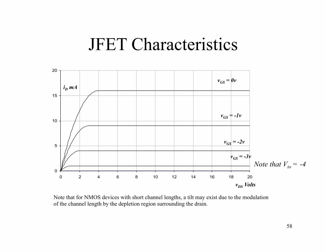
JFET Characteristics
Note that for NMOS devices with short channel lengths, a tilt may exist due to the modulation of the channel length by the depletion region surrounding the drain.
0
5
10
15
20
0 2 4 6 8 10 12 14 16 18 20
vDS Volts
iD mA vGS = 0v
vGS = -1v
vGS = -2v
vGS = -3v Note that Vto = -4

59
Regions of the JFET • Cutoff: vGS < Vto, iD =0 • Triode: vGS ≥ Vto, 0 ≤ vDS< vGS- Vto, iD=K[2(vGS-Vto)vDS-vDS
2]
• Saturation: vGS ≥ Vto and vDS ≥ vGS - Vto, iD=K(vGS-Vto)2 – Manufacturer’s parameter: Zero-Bias Saturation
Current which is the drain current at saturation when vGS = 0: IDSS= KVto
2
• Breakdown: this region is associated with high values of vDS when the junction between gate and drain breaks down and drain current increases very rapidly.
vDS
iD

60
Device Power Considerations • Static or Quiescent Power
– This is power consumed after the device has reached a logic 0 or logic 1.
– In general, when a device is in a high state, the device is not conducting (i.e., open) and the output is equal to the VOH (i.e., the supply voltage). In this case, no power is consumed.
– However, when a device is in a low state, the device is conducting (i.e., closed) and the output is equal to the VOL. In this case, there is (static) power being consumed.
– Therefore, when designed ICs we need to understand the requirements for the power supply and temperature characteristics of the devices.
• Dynamic Power Dissipation – Since the fan out load on a gate has a significant capacitive
component, a non-zero switching time will be experienced. During this period the device will dissipated power.
– The power dissipated for a device being switch at a frequency f is given below and is highly dependent on f.
AA
VSS
AA
VSS
C
VSS
periods switching theduring dissipatedpower theis
state low the toswitching wellreleased as wellas statehigh theachieve toneededenergy theis
reached ishigh when ecapacitanc on the charge theis
2
2
SS
SSSS
SS
fCVP
CVQVE
CVQ
=
==
=
VOH AA
VSS
VOL

61
Complementary MOS CMOS
• Taking NMOS (n-channel) and PMOS (p-channel) and using them in a complementary fashion (same characteristics) such that the static power is always zero (there will, of course, be dynamic power dissipated).
• Note that VGSP = vi-VDD and VGSN = vi
S
D G
S
D
G
VDD=5 V
+
vo __
+
vi __
PMOS
NMOS
Capacitance of the gates
PMOS ON when vi = 0 and vGSP = -VDD vo =VDD = VH But no static power
VDD=5 V
NMOS OFF when vi = vGSN=0
PMOS OFF when vi >0 =VDD=VH and vGSP ≈ 0
VDD=5 V
NMOS ON when vi = vGSN > 0 =VH = VDD vo = 0 But no static power

62
Graphical Analysis
• PointsCthroughD:vi=2.5andistheintersectionofvGSN=2.5andvGSP=-2.5wheretheNMOSandthePMOSarebothinsaturation.
iDN mA
0
50
100
150
200
250
0 1 2 3 4 5 vDSN V
vGSN= vi=3
vGSN= vi=2.5
vGSN= vi=2
vGSN= vi=1.5
vGSN< Vton
vi=2, vGSP= -3
vi=2.5, vGSP= -2.5
vi=3, vGSP= -2
vi=5, vGSP= 0 < Vtop A
B
C D
E
F
• ForCMOS,theloadlineoftheNMOSisthecharacteristiccurvesofthePMOS.
• Letviewtheoperationasvigoesfrom0to5V
• PointA:vi=0,theNMOSiscutoffsincevi=vGSN<Vton;thePMOSisconductingsincevGSP=vi-VDD=-VDD
• PointB:vi=2andistheintersectionofvGSN=2andvGSP=-3wheretheNMOSisinsaturationandthePMOSisinthetrioderegion.
• PointF:vi=5,theNMOSisconductingbutthePMOSiscutoffsincevGSP<Vtop=vi-VDD=0
• PointEvi=3andistheintersectionofvGSN=3andvGSP=-2wheretheNMOSisinthetrioderegionandthePMOSisinthesaturationregion.
-5 - 4 -3 -2 -1 0 PMOS

63
Transfer Characteristics
• These characteristics approach the ideal characteristics we discuss previously.
• For vi < Vton, vo = VDD
• For vi > VDD - |Vtop|, vo = 0 • The transfer characteristics fall
abruptly at vi=VDD/2 0
1
2
3
4
5
6
0 1 2 3 4 5 6vi
vo
F
A B
C
D E

64
CMOS Inverter Truth Table
S
D G
S
D
G
VDD=5 V
+
vo __
+
vi __
PMOS
NMOS
NMOS PMOSHigh 1 ON OFF Low 0Low 0 OFF ON High 1
vov i

65
CMOS NOR and NAND GATES VDD
NB
PA
NA
A
B
BAC +=
PB
NB
VDD
NA A
B
ABC =
PA PB
NOR Gate
NAND Gate
PBPAPsideNBNANside
•=+=
PBPAPsideNBNANside
+=•=
NA PA NB PB Nside Pside0 Low 0 Low OFF ON OFF ON OFF ON High 10 Low 1 High OFF ON ON OFF OFF ON High 11 High 0 Low ON OFF OFF ON OFF ON High 11 High 1 High ON OFF ON OFF ON OFF Low 0
voA B
NA PA NB PB Nside Pside0 Low 0 Low OFF ON OFF ON OFF ON High 10 Low 1 High OFF ON ON OFF ON OFF Low 01 High 0 Low ON OFF OFF ON ON OFF Low 01 High 1 High ON OFF ON OFF ON OFF Low 0
voA B
66
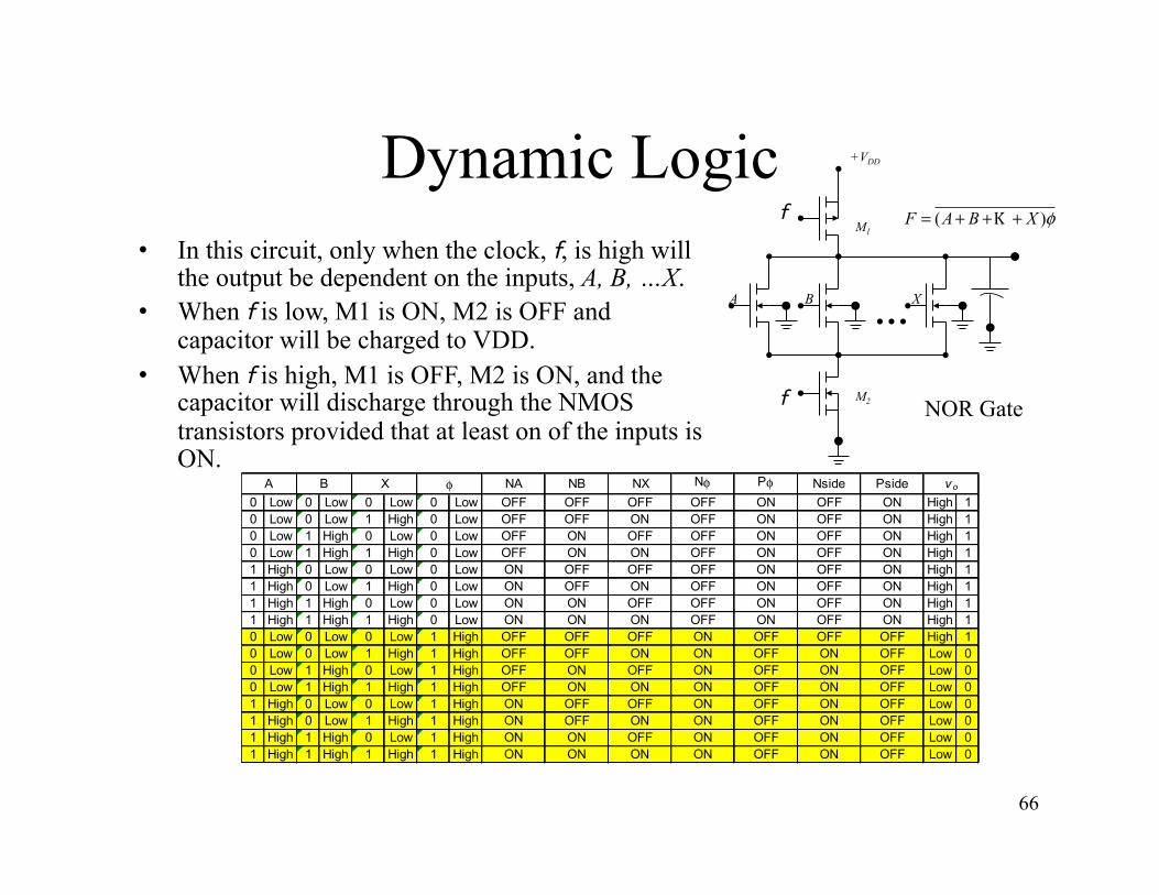
Dynamic Logic • In this circuit, only when the clock, f, is high will
the output be dependent on the inputs, A, B, …X. • When f is low, M1 is ON, M2 is OFF and
capacitor will be charged to VDD. • When f is high, M1 is OFF, M2 is ON, and the
capacitor will discharge through the NMOS transistors provided that at least on of the inputs is ON.
… X A B
M2
M1
NOR Gate
f
f
+VDD
( )F A B X φ= + + +K
NA NB NX Nφ Pφ Nside Pside0 Low 0 Low 0 Low 0 Low OFF OFF OFF OFF ON OFF ON High 10 Low 0 Low 1 High 0 Low OFF OFF ON OFF ON OFF ON High 10 Low 1 High 0 Low 0 Low OFF ON OFF OFF ON OFF ON High 10 Low 1 High 1 High 0 Low OFF ON ON OFF ON OFF ON High 11 High 0 Low 0 Low 0 Low ON OFF OFF OFF ON OFF ON High 11 High 0 Low 1 High 0 Low ON OFF ON OFF ON OFF ON High 11 High 1 High 0 Low 0 Low ON ON OFF OFF ON OFF ON High 11 High 1 High 1 High 0 Low ON ON ON OFF ON OFF ON High 10 Low 0 Low 0 Low 1 High OFF OFF OFF ON OFF OFF OFF High 10 Low 0 Low 1 High 1 High OFF OFF ON ON OFF ON OFF Low 00 Low 1 High 0 Low 1 High OFF ON OFF ON OFF ON OFF Low 00 Low 1 High 1 High 1 High OFF ON ON ON OFF ON OFF Low 01 High 0 Low 0 Low 1 High ON OFF OFF ON OFF ON OFF Low 01 High 0 Low 1 High 1 High ON OFF ON ON OFF ON OFF Low 01 High 1 High 0 Low 1 High ON ON OFF ON OFF ON OFF Low 01 High 1 High 1 High 1 High ON ON ON ON OFF ON OFF Low 0
voA B X φ

67
One More Example ( )F AB C DE φ= + +
D A
C
M1
f
M2 f
+VDD
B E
• Usingthisdesign,wecandesignotherlogicfunctions.
A B C D E P Nφ A B C D E M2 M1 NA NB NC NC NE (NA*NB+NC+ND*NE)M2 M11 0 0 0 0 0 ON OFF OFF OFF OFF OFF OFF OFF OFF ON 11 0 0 0 0 1 ON OFF OFF OFF OFF OFF ON OFF OFF ON 11 0 0 0 1 0 ON OFF OFF OFF OFF ON OFF OFF OFF ON 11 0 0 0 1 1 ON OFF OFF OFF OFF ON ON ON OFF OFF 01 0 0 1 0 0 ON OFF OFF OFF ON OFF OFF ON OFF OFF 01 0 0 1 0 1 ON OFF OFF OFF ON OFF ON ON OFF OFF 01 0 0 1 1 0 ON OFF OFF OFF ON ON OFF ON OFF OFF 01 0 0 1 1 1 ON OFF OFF OFF ON ON ON ON OFF OFF 01 0 1 0 0 0 ON OFF OFF ON OFF OFF OFF OFF OFF ON 11 0 1 0 0 1 ON OFF OFF ON OFF OFF ON OFF OFF ON 11 0 1 0 1 0 ON OFF OFF ON OFF ON OFF OFF OFF ON 11 0 1 0 1 1 ON OFF OFF ON OFF ON ON ON OFF OFF 01 0 1 1 0 0 ON OFF OFF ON ON OFF OFF ON OFF OFF 01 0 1 1 0 1 ON OFF OFF ON ON OFF ON ON OFF OFF 01 0 1 1 1 0 ON OFF OFF ON ON ON OFF ON OFF OFF 01 0 1 1 1 1 ON OFF OFF ON ON ON ON ON OFF OFF 01 1 0 0 0 0 ON OFF ON OFF OFF OFF OFF OFF OFF ON 11 1 0 0 0 1 ON OFF ON OFF OFF OFF ON OFF OFF ON 11 1 0 0 1 0 ON OFF ON OFF OFF ON OFF OFF OFF ON 11 1 0 0 1 1 ON OFF ON OFF OFF ON ON ON OFF OFF 01 1 0 1 0 0 ON OFF ON OFF ON OFF OFF ON OFF OFF 01 1 0 1 0 1 ON OFF ON OFF ON OFF ON ON OFF OFF 01 1 0 1 1 0 ON OFF ON OFF ON ON OFF ON OFF OFF 01 1 0 1 1 1 ON OFF ON OFF ON ON ON ON OFF OFF 01 1 1 0 0 0 ON OFF ON ON OFF OFF OFF ON OFF OFF 01 1 1 0 0 1 ON OFF ON ON OFF OFF ON ON OFF OFF 01 1 1 0 1 0 ON OFF ON ON OFF ON OFF ON OFF OFF 01 1 1 0 1 1 ON OFF ON ON OFF ON ON ON OFF OFF 01 1 1 1 0 0 ON OFF ON ON ON OFF OFF ON OFF OFF 01 1 1 1 0 1 ON OFF ON ON ON OFF ON ON OFF OFF 01 1 1 1 1 0 ON OFF ON ON ON ON OFF ON OFF OFF 01 1 1 1 1 1 ON OFF ON ON ON ON ON ON OFF OFF 0
F

68
Homework • NMOS Transistors
– Problems: 5.3, 5.4, 5.6
• Load-line Analysis – Problems: 5.14-17
• JFETs – Problems: 5.56, 5.57, 5.65
• CMOS – Problems: 6.48-6.50 6.69-6.70, 6.71-73