Embed Size (px)
Citation preview

PROCEEDINGS
of the
Inaugural Meeting
Florida Cluster for Advanced Smart Sensor Technologies (FCASST)
a joint USF Physics / UF MSE initiative
funded by the
Florida State University System Board of Governors
(New Florida 2010 Clustering Grant)
December 9, 2010
University of South Florida
Tampa, FL 33620

LIST OF ATTENDEES
Matthias M. Batzill, Assistant Professor, Department of Physics, USF
Elliot P. Douglas, Associate Professor, Materials Science and Engineering Department, UF
Donald T. Haynie, Associate Professor, Department of Physics, USF
Xiaomei Jiang, Assistant Professor, Department of Physics, USF
Jacob L. Jones, Assistant Professor, Materials Science and Engineering Department, UF
Sergey Lisenkov, Research Assistant Professor, Department of Physics, USF
Wm. Garrett Matthews, Associate Professor, Department of Physics, USF
Casey W. Miller, Assistant Professor, Department of Physics, USF
Pritish Mukherjee, Professor and Chair, Department of Physics, USF
George S. Nolas, Professor, Department of Physics, USF
Ivan I. Oleynik, Associate Professor, Department of Physics, USF
Simon R. Phillpot, Professor and Chair, Materials Science and Engineering Department, UF
Inna Ponomareva, Assistant Professor, Department of Physics, USF
Franky So, Professor, Materials Science and Engineering Department, UF
Hariharan Srikanth, Professor, Department of Physics, USF
Sarath Witanachchi, Professor, Department of Physics, USF
Lilia M. Woods, Professor, Department of Physics, USF
Jiangeng Xue, Associate Professor, Materials Science and Engineering Department, UF
Vasily Zhakhovsky, Research Associate Professor, Department of Physics, USF

Inaugural LaunchInaugural Launch(December 9, 2010)
Florida Cluster for Advanced Smart S T h l iSensor Technologies
(FCASST)a joint USF Physics /UF MSE initiative
funded by the Florida SUS BOG (New Florida 2010 Clustering Grant)
Pritish MukherjeePritish MukherjeeProfessor and Chair of Physics
University of South Florida, Tampa

New Florida 2010
The initiative:
http://www.flbog.org/new_florida/_docs/New_FloridaO i df_Overview.pdf
The awards announcement:
http://flbog.edu/pressroom/news.php?id=369

FCASSTFCASST
Mission:Mission:
Scientists and engineers from the Department ofPhysics at the University of South Florida (USF)Physics at the University of South Florida (USF)and the Department of Materials Science andEngineering (MSE) at the University of FloridaEngineering (MSE) at the University of Florida(UF) will establish an inter‐institutional clusterdirected at the discovery, development andy poptimization of smart sensors based on advancesin materials science and technology.

FCASSTFCASST
Key features:y f
• Nucleate inter‐institutional research collaborationsbetween a unique Applied Physics doctoral program atUSF and a highly‐ranked MSE program at UF
• Leverage existing expertise and infrastructure at UFand USF with complementary synergies spanning thep y y g p grange from fundamental science to engineeringapplications.

FCASSTAnticipated outcomes:Anticipated outcomes:• Establishing an interdisciplinary nationally prominent research effort in
sensor technology
• Generation of increased external funding
• Research spin‐offs and related economic development in Floridap p
• Enhanced graduate and undergraduate research opportunities in our SUS
• Enhanced ability to attract highly qualified graduate students, scientists, engineers and faculty to Florida
• Training of a technologically sophisticated workforce in an area of national• Training of a technologically sophisticated workforce in an area of national need
• Viability beyond State‐funding through external grants and recurring university support

Vision for FCASST• DEMAND: The science and technology of sensors is driven by increasing demand for faster,
cheaper, smaller, and more sensitive means to monitor the chemical, biological, and physicalld dworld around us.
• INTERDISCIPLINARY: The technology of sensors cuts across the disciplines of physics,chemistry, biology and engineering.
• GLOBAL IMPACT: Sensors have impact in many areas that include environmental cleanup,industrial process control, emissions monitoring, nonproliferation of weapons, screening forexplosives and contraband, home and workplace safety, medical diagnosis and care,
i l d d l l iaeronautical and space systems, and planetary exploration.
• FUNCTIONALITY: A “smart sensor” with built‐in intelligence in the form of a processorprovides added functionality beyond the primary function of sensing changes. This may
l d l f f d hinclude wireless transmission of information or producing a corrective response whensensors are integrated with MEMS.
• MATERIALS ARE THE KEY: The design, fabrication, and construction of smart structures whichare suitable for a diversity of sensing applications relies on a fundamental understanding ofhow materials ‐ the building blocks of sensors, respond to changes that are to be detected.
• WHY US? The proposed FCASST brings together existing expertise at USF and UF includingwell‐established materials design and development programs, and considerable strength inthe fabrication of device structures and prototyping to launch a coherent project towardsdeveloping the next generation of smart sensors.

FCASSTAreas for nucleating inter‐university research:
(i) Electronic structure and molecular dynamics simulations of potential sensor materials
(ii) Growth of quantum‐confined nanostructures, thin films, single(ii) Growth of quantum confined nanostructures, thin films, single crystals, composites, bulk materials and heterostructuresrelevant for sensors
(iii) Physical, chemical and biological characterization of sensor(iii) Physical, chemical and biological characterization of sensor materials
(iv) Novel concepts and device fabrication(v) Prototype development for translation of fundamental research(v) Prototype development for translation of fundamental research.

Specific Impact of FCASST
Near‐term (based on existing synergistic strengths at USF and UF):• Advanced complex oxide and magneto‐electric sensors for
biomedical and microelectronics applications • Common platform GaN/AlGaN transistor structures for gas sensing
and cancer markers detection devices• Gamma‐ray semiconductor detectors for National Security and
WMD detection applicationsWMD detection applications• Organic semiconductor‐based gas sensors• Functionalized carbon nanotubes and nanoparticles for gas and
chemical sensingchemical sensing.
Possible future efforts:• Novel materials fabrication and instrumentation development for• Novel materials fabrication and instrumentation development for
integrated multifunctional devices• Health monitoring of structures• Development of electromagnetic sensors for the detection ofDevelopment of electromagnetic sensors for the detection of
biological and chemical contamination in the marine environment

FCASST Managementg
Overall Administrative Cluster Direction‐FCASST will be jointly directed by Dr. Pritish Mukherjee, Chair, Department of Physics, USF, and Dr. Simon Phillpot, Chair, Department of Materials Science and Engineering, UF. p g g,
Technical Cluster DirectionTechnical Cluster Direction‐The technical direction of FCASST and inter‐universitycoordination will be maintained through a joint FCASSTSteering Committee comprising Drs Sarath WitanachchiSteering Committee comprising Drs. Sarath Witanachchi(USF), Steve Pearton (UF), Hariharan Srikanth (USF), Juan C.Nino (UF), George Nolas (USF), and Susan Sinnott (UF).

Potential Research Directors and Participating Laboratories
• The Nanophysics and Surface Science Laboratory (USF; Dr. Matthias Batzill)p y y ( ; )• Nanomedicine and Bionanotechnology Laboratory (USF; Dr. Donald Haynie)• Nanostructure Optoelectronics Laboratory (USF; Dr. Xiaomei Jiang)• The Bio‐Nano Research Group (USF; Dr. Garrett Matthews)
L b t f Ad d M t i l S i d T h l (USF D P iti h• Laboratory for Advanced Materials Science and Technology (USF; Drs. Pritish Mukherjee and Sarath Witanachchi)
• Spintronics Laboratory (USF; Dr. Casey Miller)• Novel Materials Laboratory (USF; Dr. George S. Nolas)• Materials Simulation Laboratory (USF; Dr. Ivan I. Oleynik)• Computational Soft‐matter Laboratory (USF; Dr. Sagar A. Pandit)• Computational Condensed‐matter Physics and Materials Science Program (USF; Dr.
Inna Ponomareva))• Functional Materials Laboratory (USF; Dr. Hariharan Srikanth)• Advanced Materials and Devices Theory Group (USF; Dr. Lilia M. Woods)• Florida Institute for Sustainable Energy Prototyping Laboratory (UF, Dr David P.
Norton)Norton)• Electromechanics Research Group (UF, Dr. Jacob L. Jones)• Major Analytical Instrumentation Center (UF, Dr. Luisa A. Dempere)• Florida Laboratory for Advanced Materials Engineering Simulation (UF, Dr. Simon
Phillpot Dr Susan B Sinnott)Phillpot, Dr. Susan B. Sinnott)• Nanoscale Research Facility (UF, Dr. Bill Appleton)• Organic Electronic Materials and Devices Laboratory (UF, Dr. Franky So)

Key Milestones
Ti t bl f d t d tiTimetable of dates and actions:
Dec. 2010‐Mar. 2011 Recruitment of Research Faculty (atUSF) d P d l R h (USF) and Postdoctoral Researchers (atUF) through nationally advertisedsearch processes; identification ofgraduate students at USF and UFgraduate students at USF and UF
Dec. 2010‐Dec. 2011 Monthly (virtual) and quarterly (in‐person) meetings of Cluster Directorsand FCASST Technical Steeringand FCASST Technical SteeringCommittee at USF and UF
Jan. 2011 – Dec. 2011 Initiation and implementation of jointresearch projectsresearch projects
Jan. 2011 – Dec. 2011 Initiation and implementation ofcluster seminars at USF and UF
Aug 2011 – Dec 2011 Meetings with potential industrialAug. 2011 Dec. 2011 Meetings with potential industrialpartners

Key MilestonesDeliverables:
January 2011 Formal establishment of FCASST between USF and UF and national announcement (including cluster website and advertised searches)and advertised searches)
March 2011 4 Research Faculty, postdocs and identified graduate students join FCASST
J 2011 D il d h i l l f ll hJanuary 2011 Detailed technical plans for all research programs initiated
January 2011 Initiation of joint USF/UF seminar seriesApril 2011 Detailed technical plans for all research programs
completedDec. 2011 Identification of industrial partnersDec. 2011 First annual report including evidence of research
progress to be assessed by publications, external grant funding, proposal submissions for external funding, t t di l d i t bli hipatent disclosures, and progress in establishing
industrial contact

Agenda for Inaugural MeetingFlorida Cluster for Advanced Smart Sensor Technologies (FCASST)
(a Florida SUS BOG‐funded joint USF Physics/UF MSE 2010 New Florida Cluster) Location: BSF 102 University of South Florida TampaLocation: BSF 102, University of South Florida, Tampa
Thursday, December 9, 2010
10:00 am – 10:30 am Opening remarks from FCASST co‐Directors (Pritish Mukherjee, USF and Simon Phillpot, UF)
Technical presentations 10:30 am – 12 noon and 1:30 pm – 3:00 pm10:30 am – 10:45 am “Functional magnetic materials”, Hariharan Srikanth, USF Physics10:30 am 10:45 am Functional magnetic materials , Hariharan Srikanth, USF Physics10:45 am – 11:00 am “Functionalization of HEMT surfaces for gas and biochemical
sensing”, Steve Pearton, UF MSE11:00 am – 11:15 am “New processing techniques in the research and development of
novel materials for energy‐related technologies”, George S. Nolas,novel materials for energy related technologies , George S. Nolas, USF Physics
11:15 am – 11:30 am “Infrastructure enhancement and stewardship”, Elliot Douglas, UF MSE
11:30 am – 11:45 am “Piezoelectric and magnetic nanostructures for smart sensors”11:30 am 11:45 am Piezoelectric and magnetic nanostructures for smart sensors , Sarath Witanachchi and Pritish Mukherjee, USF Physics
11:45 am – 12 noon “Organic semiconductors for optical and chemical sensing”, Jiangeng Xue, UF MSE
12 noon – 1:15 pm Discussions/Lunch at the Top of the Palms, USF

Agenda for Inaugural Meeting (contd.)Florida Cluster for Advanced Smart Sensor Technologies (FCASST)
(a Florida SUS BOG‐funded joint USF Physics/UF MSE 2010 New Florida Cluster)(a Florida SUS BOG‐funded joint USF Physics/UF MSE 2010 New Florida Cluster) Location: BSF 102, University of South Florida, Tampa
Thursday, December 9, 2010
1:30 pm – 1:45 pm “Ceramic materials for sensing and actuating”, Jacob Jones, UF MSE
1:45 pm – 2:00 pm “Predictive simulations of advanced sensor materials and their sensing response”, Ivan Oleynik, USF Physics
2:00 pm – 2:15 pm “Synthesis, processing and prototyping of electroceramic and semiconductor sensors”, Juan Nino, UF MSE
2:15 pm – 2:30 pm “Biopolymer‐based functional materials in medicine and biotechnology”, Donald T. Haynie, USF Physics
2:30 pm – 2:45 pm “Simulation of ionic transport and surface reactions for electrochemical systems”, Simon Phillpot and Susan Sinnott, UF MSE
2:45 pm – 3:00 pm “Toward short‐wavelength infrared sensors”, Franky So, UF MSE
3:00 pm – 3:15 pm Break3:15 pm – 3:45 pm Wrap‐up general discussion3:45 pm – 4:30 pm FCASST Technical Steering Committee meeting for future planning3:45 pm 4:30 pm FCASST Technical Steering Committee meeting for future planning
4:30 pm Adjournment

Functional Magnetic MaterialsFunctional Magnetic MaterialsFunctional Magnetic MaterialsFunctional Magnetic Materials
HariHari SrikanthSrikanth
Functional Materials LaboratoryDepartment of PhysicsUniversity of South Florida

Dr. Dr. ManhManh HuongHuong PhanPhanDr Dr HariHari SrikanthSrikanth ggDr. Dr. SusmitaSusmita PalPalDr. Dr. SrinathSrinath SanyadanamSanyadanam%%
Dr. Dr. PankajPankaj PoddarPoddar **% % Now a faculty member in HyderabadNow a faculty member in Hyderabad
AnuragAnurag ChaturvediChaturvediNicholas BinghamNicholas BinghamSayanSayan ChandraChandra
Dr. Dr. HariHari SrikanthSrikanthProfessorProfessor
Our group’s current focus areas….Our group’s current focus areas….
% % Now a faculty member in HyderabadNow a faculty member in Hyderabad* Now a Staff Scientist at NCL, India* Now a Staff Scientist at NCL, India
SayanSayan ChandraChandraKristen Kristen StojakStojakPaige Paige LampenLampenNicholas Nicholas LauritaLaurita (UG)(UG)
•• Magnetic NanostructuresMagnetic Nanostructures•• Complex oxidesComplex oxidesGi tGi t M t i dM t i d
g pg pDariaDaria KarpenkoKarpenko (UG)(UG)
MarienetteMarienette Morales (MS 2009Morales (MS 2009Natalie Frey (PhD 2008)Natalie Frey (PhD 2008)••Giant Giant MagnetoimpedanceMagnetoimpedance
• FerrofluidsFerrofluids•• MultiferroicsMultiferroics•• Interplay of magnetism andInterplay of magnetism and
Natalie Frey (PhD 2008)Natalie Frey (PhD 2008)RankoRanko HeindlHeindl (PhD 2006)(PhD 2006)Jeff Sanders (Ph D 2006)Jeff Sanders (Ph D 2006)Drew Rebar (MS 06)Drew Rebar (MS 06)Ch ilCh il Si b lSi b l (MS 06)(MS 06)•• Interplay of magnetism andInterplay of magnetism and
superconductivitysuperconductivityChamilaChamila SiyambalaSiyambala (MS 06)(MS 06)Jessica Wilson (MS 04)Jessica Wilson (MS 04)

Ordered nanostructures for EM applicationsOrdered nanostructures for EM applications
Intrinsic: μ, ε
Extrinsic:Microstructure, grain size, texture,defects
• Better control on a local scale10 μ___20 nm
• Tailored EM characteristics• Nanostructured materials
μ

Schemes for active material structures for tunable RF applicationsSchemes for active material structures for tunable RF applications
Magnetic NanoparticlesMagnetic NanoparticlesFerroelectric polymer
substrate
μεμ
=ZTunabilityTunability
MagneticMagneticDielectricDielectric MagneticMagneticDielectricDielectric
LOGO


GrapheneGraphene as a functional conducting substrateas a functional conducting substrate
5-10 layer graphene sheet synthesized by CVD technique1 using Ni substrate.
8 nm Fe3O4 NPs synthesized by chemical co-precipitation method2.
1- 10 layers of NPs were patterned by controlled LB technique on graphene sheet.
1. Qingkai Yu et.al. Appl. Phys. Lett. 93, 113103 (2008)Single layer graphene flake ~1µm length2. Sun S and Zeng H J. Am. Chem. Soc. 124 8204–5 (2002)
Single layer graphene flake 1µm length

Transverse susceptibility using a resonant RF TDO methodTransverse susceptibility using a resonant RF TDO method
•• UltrastableUltrastable Tunnel Diode Tunnel Diode OscillatorOscillator
•• LC Tank circuit selfLC Tank circuit self--resonant at ~ resonant at ~ 10 10 –– 25 MHz25 MHz
O PPMSO PPMS•• Operates in a PPMSOperates in a PPMS
•• Sensitivity 1Sensitivity 1--10Hz in 25 MHz10Hz in 25 MHz
•• Temperature range: 2K < T < 300KTemperature range: 2K < T < 300K
•• Variable DC field: 0 < H < 7TVariable DC field: 0 < H < 7T
••P. Poddar, G. T. Woods, S. Srinath and H. Srikanth, IEEE Trans. Nanotech. P. Poddar, G. T. Woods, S. Srinath and H. Srikanth, IEEE Trans. Nanotech. 44, 59 (2005), 59 (2005)••P. Poddar, J. L. Wilson, H. Srikanth, D. F. Farrell, S. A. Majetich, PRB P. Poddar, J. L. Wilson, H. Srikanth, D. F. Farrell, S. A. Majetich, PRB 6868, 214409 (2003), 214409 (2003)

Hkswitching-Hk
switching field
• Aharoni, 1957
ZP
dM=χ
h =H/HK
H 2K/M H
HDC
ZP dH
χ
⎟⎟⎠
⎞⎜⎜⎝
⎛=
z
xT dH
dMχ
Hk=2K/Ms Hrf
⎠⎝ z

Magnetoimpedance Effect (MIE)
System:Home built Helmholtz coilKepco bipolar power supplyF t i l t t
• MSE172, 146 (2010)• Phys. B 405, 2836 (2010)
Research:
Four-terminal contactField up to 120 OeFrequency 0.1-13MHz
(Co1-xFex)89Zr7B4 (x = 0, 0.025, 0.05, 0.075 and 0.1) nanocomposite ribbons
• JAP 2010 (in press)• JAP 2010 (in press)

Magnetocaloric effect (MCE)Magnetocaloric effect (MCE)Magnetic refrigerationMagnetic refrigeration
T T+ΔT
Type VIIIType I
Eu8Ga16Ge30 clathrates
New Record
ΔQΔQ
TT-ΔT
M ll R l ti
Bruck et al., Nature 415 (2002) 150
dHT
HTMHTS
H
M ∫ ⎟⎠⎞
⎜⎝⎛
∂∂
=Δ0
00
),(),( μ
Maxwell Relation
Novel composite materials for magnetic refrigeratorsT
H
M ∫ ⎠⎝ ∂0
00 )( μ
APL 93, 252505 (2008); JAP 107, 09A910 (2010)

Magnetism in complex oxides probed by MCEMagnetism in complex oxides probed by MCE
dHHTM
HTSH
∫ ⎟⎞
⎜⎛ ∂
=Δ0 ),(
)( μ
Maxwell Relation Probing phase coexistence and multiple transitions Probing phase coexistence and multiple transitions
dHT
HTSH
M ∫ ⎟⎠
⎜⎝ ∂
=Δ0
00 ),( μ
Fundamental research toolFundamental research tool
La5/8-yPryCa3/8MnO3
y = 0.275
u da e ta esea c toou da e ta esea c too
Pr0.5Sr0.5MnO3
Pr0.5Sr0.5MnO3
JAP 106, 023909 (2009)JAP 106, 023909 (2009) PRB PRB 81, 09441381, 094413 (2010)(2010)

Th F i l M i l G @ USF Th F i l M i l G @ USF The Functional Materials Group @ USF The Functional Materials Group @ USF ……
…thanks you for your attention

Functionalization of HEMT surfaces for Gas and Biochemical Sensing (Fan Ren, Chem Eng and Steve Pearton, MSE)
• Currently, the functionalization of gateless GaN/AlGaN high electron mobility transistors (HEMTs) is based on
• a catalytic metal (for gas sensing, eg. Pt and Pd catalytically dissociate H2)
• antibody-antigen pairs• enzymesyThe detection is based on charge transfer in all cases.

Hydrogen Sensing- NASA, cars, industrial processes
Ti/Al/Pt/AuTi/Au
Pt
AlGaN
GaN
Sapphire
AlGaN
Source
Gate Drain
Source

Robust Detection of Hydrogen Using Differential AlGaN/GaN Sensing DiodesAlGaN/GaN Sensing Diodes

Wireless Monitoring of Hydrogen Detection
http://ren.che.ufl.edu/app/default.aspx
D t t d C W k
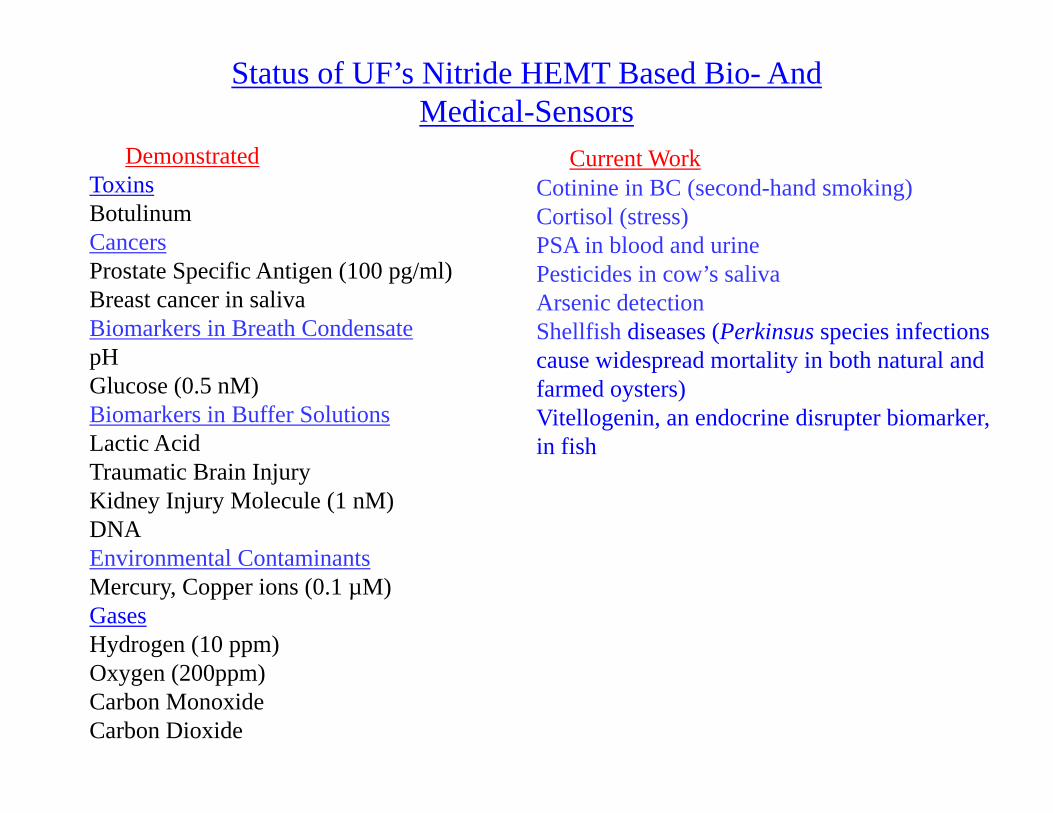
Status of UF’s Nitride HEMT Based Bio- And Medical-Sensors
DemonstratedToxinsBotulinumCancers
Current WorkCotinine in BC (second-hand smoking) Cortisol (stress)PSA in blood and urine
Prostate Specific Antigen (100 pg/ml)Breast cancer in salivaBiomarkers in Breath CondensatepH
PSA in blood and urinePesticides in cow’s salivaArsenic detectionShellfish diseases (Perkinsus species infections
id d t lit i b th t l dpH Glucose (0.5 nM)Biomarkers in Buffer SolutionsLactic Acid
cause widespread mortality in both natural and farmed oysters)Vitellogenin, an endocrine disrupter biomarker, in fish
Traumatic Brain InjuryKidney Injury Molecule (1 nM)DNA Environmental ContaminantsEnvironmental ContaminantsMercury, Copper ions (0.1 µM)GasesHydrogen (10 ppm)Oxygen (200ppm)Carbon Monoxide Carbon Dioxide

Botulinum Toxin Detection
4
5
6
ID
S (A
)
1
2
3
urre
nt
chan
ge
505
0.1 1 10 1000C
u
Botulinum toxin concentration (ng/ml)
580
495
500
505Botulinum Toxin
1 ng/ml
0.1 ng/mlPBS PBS
A) 575
580Recycled by PBS wash (pH=5)
PBS
20 / l1 ng/ml
0.1 ng/mlPBSA
)
490
495
100 ng/ml
10 ng/ml
1 ng/ml
I DS (
565
570
Botulinum toxin
20 ng/ml
10 ng/ml
5 ng/ml
I DS (A
0 200 400 600485
Time (sec)0 200 400 600 800
560
Time (sec)

Prostate Specific Antigen Detection

Fast Electrical Detection of Breast Cancer MarkerWorldwide, breast cancer is the ,second most common type of cancer and the fifth most common cause of cancer death (after lung cancer stomach(after lung cancer, stomach cancer, liver cancer, and colon cancer).The tests used for screening, diagnosis, and monitoring, including mammograms, ultrasound, MRI, CAT scans, PET scans usually at centralizedPET scans, usually at centralized locations –lacking in developing countries

Electrical Response of Breast Cancer Marker c-erbB-26
844
848 PBS
16.7 µg/mL2 µg/mL
0.25 µg/mL
A) 4
5
6
DS (µ
A)
836
840 I DS(
µA
1
2
3
Cha
nge
of I D
0 100 200 300 400
832
time (sec)0.1 1 10 100
0
1
c-erbB-2 antigen concentration (µg/ml)
Test samples Concentration Source c-erbB-2 10-200 units/ml Oncogene Research -
Prognostic breast markers
c erbB 2 10 200 units/ml Oncogene Research Human ErbB2/Fc 1129-ER (100 μg/mL) with Ab (C-ErbB2)
EGFR 0.5-3 fmol/ml Triton Diagnostic, Inc.p53 0.1-200 pmol/ml Oncogene ResearchCA-15-3 1-30 units/ml CIS Biointernal

Glucose Detection in Breath Condensate
20
15
no enzyme with enzyme
ds (
A)
5
10
Cha
nge
of I d
100 101 102 103 104 105
0
Concentration (nM)

Wireless pH and Biosensor
Sensor
Nordic2.4Ghz
TransceiverBatter
y 3.5”
0.
• Pen-sized portable, re-configurable wireless transceiver integrated with pH sensor has been designed
MSP430F2013PowerManagement
.6”pH sensor has been designed and fabricated
• The transmitter and receiver pair is designed to operate at 2 4GH ith f t2.4GHz with range of up to 20ft line-of-sight
• The wireless circuits only consume a power level around 1 W
AC Wall Transformer
Regulator Regulator
Battery Backup Control
Internet
Cell Phone
Microcontroller
Battery/Energy Harvest
Battery Backup Control
Sensor
Microcontroller
Reference
ZigBee
Transceiver
Wireless Network ServerInternet Server

ConclusionsAdvantages of Semiconductor Biosensors
• G N d i t h l i i ll il bl (bl / /UV LED d l )• GaN device technology is commercially available (blue/green/UV LEDs and lasers), materials chemically stable and can be operated at elevated temperature• Sensor signals are amplified through HEMT- excellent sensitivity• Sensor provides digital signal v.s. fluorescence measurement -p g gwireless capability- fast response
• Small size of each individual sensor; less than 100 µm2 - low cost and small sample size• Different sensors can be integrated on a single chip•Calibration sing differential pair sensors•Calibration using differential pair sensors•Easily transportable and can be integrated with wireless, encrypted data systemsDisadvantages•More testing of realistic samples, followed by field trials (initial work commenced with Florida Diabetic Summer camp-) http://www.floridadiabetescamp.org/•Some surface functional layers not stable for long periods-need a clinical environment•Robustness of sample collection needs to be ensured

New processing techniques in the research and p g qdevelopment of novel materials for energy-related
technologies
George S. NolasDepartment of Physics, University of South Floridap y , y
http://shell.cas.usf.edu/gnolas/

Heat Source
ThermoelectricsPhotovoltaics& Optoelectronics
Applications
P N
p
Heat Sink
LoadI
Li-ion Batteries
Magnetic RefrigerationHydrogen Storage

Multiple Synthetic Techniques
Sample
Tube Furnace
Vacuum Valveand Coupling
Quartz Tube
To Vacuum System
Th l
vacuumseal
Thermocouple
crucibleN2/Ar
S k Pl Si t i
AC
M Beekman M Baitinger H Borrmann W Schnelle K Meier
Spark Plasma Sintering
M. Beekman, M. Baitinger, H. Borrmann, W. Schnelle, K. Meier,G.S. Nolas, Y. Grin, J. Amer. Chem. Soc. 131, 9642 (2009)

Synthesizing Nanocrystals in Solution
Direct Precipitation
PbTe t l
Mixing of solutions
Micro Emulsion ~ 50-100 C
nanocrystals
SURFACTANT
Te ions in hot aqueous KOH solution Pb and Ag
ions in cold aqueous solutionSURFACTANT
PbTe, Bi2Te3and other
“ ”solution
Solvothermal
HEXANEWATERnanocrystals“ ”
Bi2Te3 nucleiEthylene glycol
solventSolvothermal
Boiling point of the solvent
Pressurized Chalcogenidenanocrystals
solvent
Bi2Te3 spherical nanocrystalsprotected by
ethylene glycol

Open-Framework Inorganic Materialsexample: Clathrates
T VIIIp
Type VIII
Type I
Polyhedral“Building Blocks”
Type II
Type I
• M. Beekman & G.S. Nolas, J. Mater. Chem. 18 842 (2008)18, 842 (2008)• G.S. Nolas et al in Semiconductors and Semimetals, Vol. 69, Academic
cP124Press, 2001

New Synthetic Techniques (patent pending)
Na24Si136Na24Si136
Na8Si46Na8Si46
“Novel Methods for Solid State Crystal Growth”, Patent Pending, Serial No. 12/859,534, submitted August 19, 2010

Physical Properties of Na24Si136
from heat capacity, Cp
from single-crystal XRD
32 4
from low-T transport
32 4/
2 20
exp( / )( ) 3 and ( ) 9
(exp( / ) 1) ( 1)D
xTEi EiEi Ei D D x
Ei D
T T x eC T N R C T N R dxT T e
Cp = Ce + CE1 + CE2 + CD where Ce = γT,
M. Beekman, W. Schnelle, H. Borrmann, M. Baitinger, Yu. Grin and G.S. Nolas, Phys. Rev. Letter 104, 018301 (2010) M. Beekman, R.P. Hermann, A. Mochel, F. Juranyi and G.S. Nolas, J. Phys.: Cond. Matter 22, 355401 (2010)S Stefanoski J Martin and G S Nolas J Phys : Cond Matter 22 485404 (2010)S. Stefanoski, J. Martin and G.S. Nolas, J. Phys.: Cond. Matter 22, 485404 (2010)S. Stefanoski, M. Beekman, W. Wong-Ng, P. Zavalij and G.S. Nolas, Chem. Mater., in press (2010)

Thermoelectric (TE) Materials and Applications
Active Cooling Heat Source
P N P N
Heat Rejection Heat Sink
ILoad
I
Refrigeration Power Generation
http://img.alibaba.com/photo/11217679/Peltier_Cooler.jpg
Applications ranging from‘Household’to ‘Space’Applications ranging from Household to Space
http://nextbigfuture.com/2007/10/thermoelectroni
http://sscooling.com/index.php?option=com content&taskhttp://embedded- 2007/10/thermoelectroni
c-potential-and-status.html
p?option=com_content&task=view&id=118&Itemid=251
pcomputing.com/tec-coupled-pump-laser
www.amerigon.com

New Directions in TE materials Research
More control of scatteringscatteringMore control of scatteringscattering
parameters,parameters, FermiFermi levellevel
position,position, carriercarrier densitydensity
parameters,parameters, FermiFermi levellevel
position,position, carriercarrier densitydensity
Electrical
T.M. Tritt and M.A. Subramanian, eL
T2
SZTFigure of
Merit
Thermopower Conductivity
Thermal Conductivity
T.M. Tritt and M.A. Subramanian, MRS Bulletin 2006, 31,188
Increase number of grain boundaries in bulk Phonon scattering Phonon scattering
eL
Enhanced S due to charge carrier filtering
Boundary scattering at the interfaces to reduce κL
Energy Filerting Energy Filerting

New Directions in TE Materials Research
Incorporate “nano-scale domains” in bulk matrixin bulk matrix
Approach
TOP-DOWN BOTTOM-UPTOP DOWN BOTTOM UP
AtomsBulk Nano N t t d
(1)
Nanostructured B lkNanograins
AtomsBulk Nano Nanostructured Bulk
(2) MeltConstituent BulkNanograinsConstituent
elements

Chemical Synthesis for TE Materials ResearchDirect PrecipitationDirect Precipitation
50 100°C
SPS
P-type PbTe nanocomposite
~ 50-100°C
Selective crystal size f 50 250
1-20% Ag doped P-type PbTe nanocrystals
from 50 nm - 250 nm
200 nm
2 ) 16
red p-type PbTe Nanocomposites , Bulk p-type PbTe
---- A.J. Crocker et al., Brit. J. Appl. Phys. 18, 563 (1967)
oeffi
cien
t ( V
/K)
300
400
1018 1019
Pow
er F
acto
r (W
/cm
K2
2
4
6
8
10
12
14
J. Martin, G. S. Nolas, W. Zhang, and L. Chen, Appl. Phys. Lett. 90, 222112 (2007)J. Martin, L. Wang, L. Chen, and G.S. Nolas, Phys. Rev. B 79, 115311 (2009)A. Popescu, L.M. Woods, J. Martin, and G.S. Nolas, Phys. Rev. B79 305302 (2009)1018 1019
See
beck
Co
100
200Carrier Concentration (cm-3)
1018 1019
PbTe nanocomposites
79, 305302 (2009)Carrier Concentration (cm-3)
1018 1019

SolvothermalChemical Synthesis for TE Materials Research
Nanocrystals of d ~ 18 3 nm>Boiling point of the solvent
Pressurized
Se doped N-type Bi2Te3
nanocrystals
Bi2Te3 nuclei
Ethylene glycol solvent
the solvent
SPS
2 3
Selective crystal i f
200
size from ~1 nm - 20 nm
V/K
)
120
140
160
180
200
A F Ioffe Semiconductor thermoelements and
n-type Bi 2Te3 Nanocomposites
ô Kim, et al, J. Alloys Comp. 399, 14 (2005)à Zhao, et al, J. Alloys Comp. 467, 91 (2009)
Bi2Te3 nanocomposites
|S| (
60
80
100
120 A. F. Ioffe, Semiconductor thermoelements and thermoelectric cooling, Infosearch Limited, 1957
Calculated S vs. n ‘Pisarenko Relation’
A. Datta, J. Paul, A. Kar, A. Patra, Z. Sun, L. Chen, J. Martin, and G. S. Nolas, Cryst. Growth Design 10 , 3983 (2010)
Carrier Concentration (cm-3)1e+19 1e+20

Infrastructure Enhancement and Stewardship

i fadvanced sensor technologies
infrastructure systems
hazard resistance
fundamental science
policy and planning decisions
lifetime and structural health
predictions decisionspredictions

Novel Electronics Environmental ExposureNovel Electronics Environmental Exposure
Materials Behavior
1 centimeter
Materials/Sensor Materials BehaviorInteractions
Policy
ModelingNew Sensors

Structural Health Monitoring
• Data collected in real time.• Current use:
- Research mode to compare b id b h i d ibridge behavior to design assumptions.
- Measure behavior with proof loadload.
- Weigh-in-motion.
Research OpportunitiesResearch Opportunities• New approaches to SHM that allow real-time analysis
of bridge health.

Sensor Technologies for SHM
• Typically strain gauges, accelerometers.
• Wiring accounts for 50% of i t ll ti t ddinstallation cost, adds considerable complexity.
• Wireless sensors need reliable power for 50+ yearsreliable power for 50+ years.
Research Opportunitiesf i ki• New types of sensors – corrosion, cracking, etc.
• Reliable power sources – low power sensors, long lifetime batteries, energy harvesting, etc., gy g,
• Wireless data transfer.

Non-Destructive Evaluation• Primarily ultrasonic ground-Primarily ultrasonic, ground-
penetrating radar.• Analysis can take months.• No ability to measure a y
structure and determine the current condition.
Research Opportunities• Techniques to use data to identify state of structure in q y
near real time (materials – sensor interactions.)• Limitations of techniques.• Development of new techniques• Development of new techniques.• Fusion of data from multiple sources.

Probabilistic Approach to SHMProbabilistic Approach to SHMNam Ho Kim
• Current methods of data analysis attempt exact calculations based on sensor data.
– Errors in sensor data, materials properties, and analytical modelsErrors in sensor data, materials properties, and analytical models make this difficult.
• Probabilistic approaches allow refinement of prediction as data is pcollected.
– Bayesian statistics to refine damage estimates in presence of errors and pnoise.
– Computational model to predict effect on prognosis.p g

Piezoelectric/Magnetic Nanostructures for Smart Sensors
and
S i d t Q t D t f N t G ti S l C llSemiconductor Quantum Dots for Next-Generation Solar Cells
Sarath Witanachchi & Pritish Mukherjee

Dual-Laser PLD with ICCD Imaging System
UV Detector0 8
1.0
ge
UV
Excimer Laser
Trig In
Sync Out
Oscilloscope
0.2
0.4
0.6
0.8
Norm
aliz
ed V
olta
g
IR
Vacuum Chamber
Substrate Heater CO2 Laser
Timing between the excimer (UV) andCO2 (IR) laser pulses for ablation
10.00ns
Digital Delay Generator
0.00 200 400 600 800 1000
Time (ns)
N
Rotating Target
IR Detector
CO2 (IR) laser pulses for ablation
Trig InICCD Sync
Control PC
Lens System
ICCDTypical:1-5 J/cm2 excimer laser1-3 J/cm2 CO2 laser1-10 Hz
248 nm wavelength KrF excimer laser, 10.6 μm CO2 laser, sub-microtorr vacuum system, PI-MAX:512 UNIGEN digital ICCD
t 400 Mh 2 GS/ ill b d
Schematic diagram of the dual-laser deposition system1 10 Hz2x3 mm laser spot size
camera system, 400 Mhz 2 GS/s oscilloscope, sub-nanoseconddigital delay generator

Single laser ablation
Dual-laser ablation with 50 ns delaywith 50 ns delay

Goal of the Project
Strain-mediated epitaxial horizontal hetero-structures of magnetic and ferroelectric phases
Hetero-epitaxy
(two phase system)
Homo-epitaxy
(single phase system)
PZT (100) Z O M (001)ZnO: V (001)
c-cut Al2O3 (001) MgO / SrTiO3 (100)
LSMO (100)
CFO (100)
ZnO (001)
ZnO: Mn (001)
ZnO: Mn-ZnO: V heterostructureCFO-PZT heterostructure

Epitaxial PZT Thin Films: Ferroelectric Properties
LSMO (100) (100 nm)
PZT (100) (500 nm)
MgO / SrTiO3 (100) substrate
LSMO (100) (100 nm)
LSMO/PZT/LSMO capacitor
100
120PZTDL- MgOPZT M O
100
120PZTDL- STOPZT STO
20
40
60
80PZTSL- MgO
(C
/cm
2 )
20
40
60
80PZTSL- STO
(C
/cm
2 )
-60
-40
-20
0
LSMO electrodes
PZT (500 nm)LSMO (100 nm)
Pola
rizat
ion
-60
-40
-20
0
LSMO electrodes
PZT (500 nm)LSMO (100 nm)
Pola
rizat
ion
-200 -160 -120 -80 -40 0 40 80 120 160 200-120
-100
-80 LSMO (100 nm)MgO(100) substrate
Electric Field (kV/cm)-200 -160 -120 -80 -40 0 40 80 120 160 200
-120
-100
-80 LSMO (100 nm)STO(100) substrate
Electric Field (kV/cm)
Uncertainty: < 1 %

Multiferroic Spin Valve Sensor for Bio‐detection
DNA coated magneticDNA‐coated magnetic nanoparticles
Free layer
Hard layer
Multiferroic spin valve
Tagging biomolecules with functionalized magnetic nanoparticles(Fe3O4) and their detection will lead to very high sensitivity in bio-detection in
The spin alignment in the free layer is affected by the attached magnetic nanoparticles. Since the magnetic and the electric polarization are coupled in very high sensitivity in bio detection in
comparison to functionalized micro-beads. In the proposed device the change in magnetoresistance (MR) of a multiferroic spin valve is used to detect
multiferroics, the application of a voltage across the ferroelectric film can change the spin valve from high to low resistive state. The applied voltage can be calibrated to multiferroic spin valve is used to detect
the magnetic nanoparticles. correspond to the number of magnetic nanoparticles attached to the device.

PZT Nano-pillar Structures as Sensors of Nano-forces and Nano-displacementsNano-displacements
Normal incidence Oblique incidence
flux
PZT nanotemplate
flux
Substrate
Steps involved in the fabrication of the PZT/RuO2 nanopillarstructure (a) formation of the PZT nanotemplate by using an
(b)(a) (c)
structure (a) formation of the PZT nanotemplate by using analumina nanotemplate, (b) oblique‐incidence deposition of PZT toform nanopillars, (c) coating nanopillars with other materials

PbSe Quantum Dot-Polymer Composite Structures for Next generation FlexibleStructures for Next-generation Flexible
Solar Cell Devices
Dissociation of e-h pair is facilitated by band bending at the QD-polymer interface – surfactants have to be removed

LAS deposition of PbSe QD films
2
1 3 542
Capped PbSe QDs in heptane
~1.5 m droplets with QDs in SF6 gas
Surfactant-free QD film formation
(1) Suspend capped PbSe QDs in a volatile solvent(2) Form an aerosol ~1.5 m diameter by a nebulizer(3) Inject the aerosol through a nozzle into a growth chamber with SF6 carrier gas(4) H t SF ith CW CO l i th l t d th f t t t(4) Heat SF6 gas with a CW CO2 laser causing the solvent and the surfactants to
evaporate(5) Deposit surfactant-free PbSe QDs on a substrate.

Self-assembled (capped) and LAS-deposited (surfactant-free) PbSe QDs( ) Q
Capped PbSe QD film by self-assembly
(a) (b(a) ()
Surfactant-free
2 nm 100 nm
Su c eePbSe QD film by LAS process

Evidence of quantum confinement by absorption spectroscopy
1 1
0.8
0.9
1
1.19.5 nm QD film by LAS 10.9 nm QDs in hexane .)
0 4
0.5
0.6
0.7
1S1D 1P
orpt
ion
(a.u
.
0.1
0.2
0.3
0.4
Abs
o
800 1200 1600 2000 2400
Wavelength (nm)

Enhanced current transport in pLAS-deposited films
400
200
300
400
nA)
Drop-casted filmLAS deposited film
25.20VII
-100
0
100C
urre
nt (n
-300
-200
-6 -4 -2 0 2 4 6
Voltage (V)

QD-based flexible solar cells
PEDOT Polymer
Optical Testing(Current density, multiple exciton generation)
GlassFTO
y
hν
TiO2 grown by a hydrothermal process

Conductivity of LAS deposited PbSe films
S)
Weak couplingh << kBT, T 100K
ln(G
/nST> 100K
Strong couplingh > k T 50
0 5 10 15 201000/T (K-1)
h > kBTT< 100K
Leads to increase in ConductanceConductance
- Tunneling rate

Organic Semiconductors for Organic Semiconductors for O ti l d Ch i l S iO ti l d Ch i l S iOptical and Chemical SensingOptical and Chemical Sensing
Jiangeng Xue
f SDepartment of Materials Science and EngineeringUniversity of Florida, Gainesville, FL, USA
([email protected], http://xue.mse.ufl.edu)(j @ , p )
FCASST, Dec. 9, 2010

Organic Organic ((OptoOpto)Electronic )Electronic MaterialsMaterials
N
N
NN
N NN Cu
nSmall molecules(Monomers)
Conjugated Polymers
N
y
Structural Complexity
Si il i f d t l h i l tiSimilar in fundamental physical propertiesHeld together by van der Waals force (much weaker than intra-
molecular covalent bonding)Different in processing techniquesDifferent in processing techniques
Small molecules: vacuum or vapor depositionPolymers: solution processes (e.g. spin coating, printing) Jiangeng Xue

Electronic Materials:Electronic Materials:O i I iO i I iOrganic vs. InorganicOrganic vs. Inorganic
Advantages of organicsCheapLow temperature processingC ibl i h fl ibl b
Low mobility
Advantages of organicsDisadvantages
Compatible with flexible substratesTunable material properties via
structure modification
yLow conductivityLow stability/reliabilityP tt i iStrong optical absorption Patterning issues
Organic semiconductors have potential application in inexpensive, large-area, flexible, and light-weight electronic
and optoelectronic devicesand optoelectronic devices.
Jiangeng Xue

Organic Electronic and Photonic DevicesOrganic Electronic and Photonic Devices• Organic photovoltaic cells for low‐cost solar energy
conversionO i li ht itti d i f li hti d di l• Organic light‐emitting devices for lighting and display applications
• Organic photodetectorsg p• Organic transistors (thin film transistors, bipolar transistors,
phototransistors)• Organic memories• Organic chemical sensors
O i b d RF ID t Solar
Data Input Data OutputOptical Power
• Organic‐based RF‐ID tags• ……
Solarcell
D t t OLEDCircuit and memory
Detector
Jiangeng Xue

OrganicOrganic‐‐based Optical Sensors (based Optical Sensors (PhotodetectorsPhotodetectors))
Ch
Large Area Flexible
Cheap
Security & Medical Imaging
Simultaneous Tomography Intelligent Vision
2
Jiangeng Xue

Multilayer Organic Multilayer Organic PhotodetectorsPhotodetectorsBCPCathode BCP
[CuPc/PTCBI]N
Cathode
ITO/[CuPc(30Å)/PTCBI(30Å)]8/BCP(150Å)/Al
Glass
Anode
40
60 Commercial ITO
0 nm
(%)
CuPc(donor)
20
40
Sputtered ITO
ext a
t =
620
Untreated
Cathode
Anode LUMO
0 -2 -4 -6 -8 -100
e
V (V)
Untreated Oxygen plasma treated UV ozone treated
BCPPTCBI
(acceptor) HOMO
VPD (V)
P. Peumans et al., Appl. Phys. Lett. 76, 3855 (2000).
Jiangeng Xue
, pp y , ( )J. Xue et al., J. Appl. Phys. 95, 1859 (2004).J. Xue et al., J. Appl. Phys. 95, 1869 (2004).

Multilayer Organic Multilayer Organic PhotodetectorsPhotodetectors –– Dark CurrentDark Current
10-2
10-1
Sputtered MTDATA
Commercialuntreated Sputtered
O l
CommercialO-plasma
treated
ITO/[CuPc(30Å)/PTCBI(30Å)]8/BCP(150Å)/Al
10-5
10-4
10-3
A/c
m2 )
10-1
V 10 V
Sputtereduntreated
MTDATA-coated
O-plasmatreated
10-8
10-7
10-6 Sputtered ITO Untreated O-plasma treated
Commercial ITO Untreated
J d (mA
10-4
10-3
10-2
m2 )
VPD = – 10 V
VPD = – 5 V
-10 -8 -6 -4 -2 0 2 410-9
10 O-plasma treated
VPD (V) 10-6
10-5
10
J d (m
A/c
VPD 5 V
V = 0 5 VCuPc
3.8 4.0 4.2 4.4 4.6 4.8 5.0 5.210-8
10-7VPD = – 0.5 V
Cathode
Anode LUMO
Jiangeng Xue
ITO work function, W (eV)BCPPTCBI
HOMO

Organic Position Sensitive DetectorsOrganic Position Sensitive DetectorsLight
Output I2
Output I1
Detector active region
Common electrode
12 IIx α15
0 V 0 7% Common electrode
5
10
tion,
x
(mm
) 0 V 0.7%-0.5 V 0.1%-1 V 0.1%1 5 V 0 8%
-5
0
d B
eam
Pos
it -1.5 V 0.8%-2 V 1.3%
F2σδ
-10
Mea
sure
d Fσ – r.m.s. deviation from regression
linear fit to dataF – full positional range of data
Jiangeng Xue
-15 -10 -5 0 5 10 15
-15
Actual Beam Position (mm)
p g
B. P. Rand et al., IEEE Photon. Technol. Lett. 2003.

Organic Photodiodes with High GainOrganic Photodiodes with High Gain
Bl ki 1 8 C60 CuPcBlocking layers
3.23 6
1.8 NTCDAC60 CuPc
BCP
CuPc x%ITOAl
BC
P4.03.6
5 2Φ ~ 4 5 eVΦ = 4.3 eV
C60 103
100W/cm2 broadband
C60 (1‐x%)
NTC
DA
6.2
5.2
6 4
Φ 4.5 eV C
101
102
m2 )
100W/cm broadband Dark
Responsivity ~ 200 A/W
Blend
8.0
6.4
10-2
10-1
100
J (m
A/c
m
10 n
m
50 n
m
8 nm
3 nm
-4 -3 -2 -1 0 1 210-3
10-2J
V (V)
Jiangeng XueW. T. Hammond and J. Xue, Appl. Phys. Lett. 97, 073302 (2010).
V (V)

Gain MechanismGain MechanismDark
1000
-4 0VDark
10
100
in (I
QE
)
4.0V -3.0V -2.5V -2.0V -1.5V
AlBCP
C60:CuPc (7:3)
0.1
1Gai -1.0V
-0.5V 0.0V
C60NTCDAITO
Illuminated
400 500 600 700 800
Wavelength (nm)
1.0Control device
Al0.6
0.8
QE
-4 V -3 V
2 V
Control device (no HBLs)
BCPC60:CuPc (7:3)
ITO0.0
0.2
0.4IQ -2 V -1 V 0 V
Jiangeng XueW. T. Hammond and J. Xue, Appl. Phys. Lett. 97, 073302 (2010).
400 500 600 700 800Wavelength

Organic Thin Film Transistor for Chemical SensingOrganic Thin Film Transistor for Chemical Sensing
Acetic acid
Gases or chemicals
Acetic acidOrganic semiconductor DrainSource
Liao et al. Sensors and Actuators B107 (2005) 849
Gate
• OTFT: easy to functionalize, low costs for large area substrates
Ethanol
g• Demonstrated H2O and pH sensing.
Cl- and SO4- sensing possible.
Jiangeng Xue

Vertical Molecular Nanostructures by Oblique Vertical Molecular Nanostructures by Oblique Angle DepositionAngle Deposition
Molecular Flux
αNanorodPCBM
CuPc(donor)
SubstrateWith rotational
substrateWith stationary
substrate
(acceptor)
ω
BCP
100 nm100 nmAl
BCP
PCBM
100 nm100 nm
ITO CuPcnanorods
Jiangeng Xue
100 nm
Y. Zheng et al., Organic Electronics (2009); IEEE J. Sel. Top. Quantum Electron. (2010); Polym. Rev. (2010).

ConclusionsConclusions• Organic semiconductors have interesting applications in
low-cost, large-area, light weight and flexible electronic d t l t i d iand optoelectronic devices.
• Multilayer organic photodiodes with gains up to a few hundred have been demonstrated with spectral coveragehundred have been demonstrated with spectral coverage across the entire visible spectrum.
• Organic semiconductors can also be used for chemical i h d i th thi fil t i tsensing when used in the thin-film transistor
configuration, and vertically aligned molecular nanorod array could be used to increase sensitivity of such y ychemical sensors.
Jiangeng Xue

Ceramic Materials for Sensing and Actuating – J. Jones
Ceramic Materials for Sensing andCeramic Materials for Sensing andCeramic Materials for Sensing and Ceramic Materials for Sensing and ActuatingActuating
with an undertone of with an undertone of in situ Xin situ X--ray and neutron diffractionray and neutron diffraction
Jacob L. JonesAssistant Professor
Department of Materials Science and EngineeringUniversity of Florida

Ceramic Materials for Sensing and Actuating – J. Jones
Jacob L. Jones Jenny Forrester P td t l
Goknur TutuncuP td t l
Anderson Prewitt Krishna Nittala Shruti SeshadriAssistant Professor Postdoctoral
AssociatePostdoctoral
AssociatePhD Candidate PhD Candidate PhD Candidate
Chris Fell Elena Aksel Isaac Krull Sungwook Mhin Tedi-Marie Usher Ben KowalskiPhD Candidate PhD Student PhD Student PhD Student PhD Student Senior Research
Humberto Foronda Lyndsey Denis Katherine Dunnigan Cassie LLano Michelle Nolan
Not yet pictured: Brian Lettman, Kevin Seymour, Michael Adams, Erik Hofstetter, and Jared Carter
University ScholarJunior
REM programSophomore
REM programSophomore
REM programSophomore
HHMI Scholar
u/g researchSophomore
HHMI Scholar

Ceramic Materials for Sensing and Actuating – J. Jones
Ceramic processing, e.g. solid state
Ceramics
Compositional investigations including lead-free and multiferroic
Ceramics
ElectromechanicsElectromechanics
Mechanics Diffraction
ElectromechanicsElectromechanics
Mechanics Diffraction
Crystal structureT t l i
Electromechanics, e.g. piezoelectricity Texture analysis
Time-dependent structure changes
piezoelectricity, ferroelectricity
Anisotropy Mechanical Behavior Microdiffraction
Synchrotron and neutron sources
Mechanical BehaviorDeformation & Fracture

Ceramic Materials for Sensing and Actuating – J. Jones
PiezoelectricsPiezoelectrics for Sensors and Actuatorsfor Sensors and Actuators
Actuating 0 04
0.00
0.04
0.08
rain
(%)
Material-800 -400 0 400 800
-0.08
-0.04St
Electric Field (V/mm)
Mechanical
Electronics
Mechanical displacement,
vibration, acoustics, etc.
Piezo-electric
Sensing Material
ElectrostaticsElectrostrictionPiezodiffusivityFlexoelectricity From DamjanovicFlexoelectricityFerroelectricityPiezoelectricity
From Damjanovic, Chapter 4 in The Science of Hysteresis (2005).
Images from various sources

Ceramic Materials for Sensing and Actuating – J. Jones
PiezoelectricsPiezoelectrics for Sensors and Actuatorsfor Sensors and Actuators
Sensors Actuators• Benefit of Piezoelectric Materials: • Benefit of Piezoelectric Materials:
ElectroactiveDielectric Acrylic
• High max operating
• Benefit of Piezoelectric Materials: • Benefit of Piezoelectric Materials:
Electroactive actuators
elastomers
N t l
yelastomerstemperatures
(<600-1000°C)
• Chemical
Magneticactuators
Natural muscle
Chemical resistance
• Reliability
Piezoelectric and magnetostrictive
actuators
actuators
After Ashley, “Artificial Muscles,” Scientific American (2003).

Ceramic Materials for Sensing and Actuating – J. Jones
PiezoelectricsPiezoelectrics for Sensors and Actuatorsfor Sensors and Actuators
Servo displacement transducers
Pulse driven actuators
Resonance transducer devices
• Interferometer dilatometer
• Deformable mirrors
• Swing CCD image sensors
• Swing pyroelectric
• Ultrasonic rotary motors• US linear motors• Automatic focusing
• Precision linear motion guide system
• Cutting error correction mechanism
• Servo valves
sensor• Linear walking machines• Micro angle adjusting
device• Dot matrix printer head
mechanism• Ultrasonic surgery knife• Piezoelectric fans• Piezoelectric pumps• Liquid atomizersServo valves
• VCR head tracking actuators
• Vibration suppression systemN i ll ti
Dot matrix printer head• Ink-jet printer heads• Piezoelectric relays• Gasoline injectors• Diesel injector system
D f bl t t l
Liquid atomizers• Piezoelectric
transformers• Surface acoustic wave
(SAW) device• Noise cancellation• Atomic force
microscope
• Deformable structural materials
After Wersing, “Applications of Piezoelectric Materials: an Introductory Review,” in Setter (2003).

Ceramic Materials for Sensing and Actuating – J. Jones
Crystallography of OxidesCrystallography of Oxides• Fast-acquisition laboratory X-ray source at the University of Florida
– Curved position-sensitive detector covering 120° in 2θ • Australian Nuclear Science and TechnologyAustralian Nuclear Science and Technology
Organisation (ANSTO)– Monochromatic neutrons– HiFAR Reactor, TASS
Lab source at UF
OPAL reactor at ANSTO
– OPAL Reactor, WOMBAT• 2009-2012 program allotment
• European Synchrotron Radiation Facility (ESRF)Radiation Facility (ESRF)
– Beamline ID-15: microdiffraction, time-resolved diffraction• Advanced Photon Source (APS)
MicrodiffractionSNS at ORNL
APS in Argonne
– Microdiffraction– Time-resolved diffraction– Mail-in program for structural refinement
• Oak Ridge National Laboratory –• Oak Ridge National Laboratory –HFIR and SNS
– WAND (high intensity), NRSF2 (stress), HB-2A (powder)

Ceramic Materials for Sensing and Actuating – J. Jones
Structure of Novel LeadStructure of Novel Lead--Free Free Pi iPi i S M t i lS M t i l
• Synthesis, high-resolution structural measurement, and refinement of
PiezoceramicPiezoceramic Sensor MaterialsSensor Materials
(1-x)Na0.5Bi0.5TiO3-xBaTiO3 (BNT-xBT) piezoelectric ceramics.• Crystallographic refinement of the NBT indicates a monoclinic Cc space
group, not widely-assumed R3c. • Implies complex ferroelectric/ferroelastic domain structure in BNT-based
piezoceramics. May explain nanodomains and relaxor-like behavior.• Also suggests “monoclinic” not a sufficient condition for high d33.gg g 33
High-resolution X-ray measurements at the Advanced Photon Source, Argonne National Laboratory

Ceramic Materials for Sensing and Actuating – J. Jones
Phase transitions inPhase transitions inPhase transitions in Phase transitions in xxNaNa0.50.5KK0.50.5NbONbO33--(1(1--xx)LiNbO)LiNbO33
Cubic(100)
Tetragonal(100)/ g(010)
(100)/(010)/
Orthorhombic(010)/(001)

Ceramic Materials for Sensing and Actuating – J. Jones
Phase transitions inPhase transitions inPhase transitions in Phase transitions in xxNaNa0.50.5KK0.50.5NbONbO33--(1(1--xx)LiNbO)LiNbO33
0.7Na0.5K0.5NbO3-0.3LiNbO30.3Na0.5K0.5NbO3-0.7LiNbO3

Ceramic Materials for Sensing and Actuating – J. Jones
CAREER: TimeCAREER: Time--resolved structureresolved structure--property property l ti hi i i l t i il ti hi i i l t i irelationships in piezoelectric ceramicsrelationships in piezoelectric ceramics
• 2008-2013S t 2+ d t d 2+ d d t t d t
800 (a)• Supports 2+ graduate and 2+ undergraduate students.• Material properties (e.g., piezoelectric and dielectric coefficients) are
often measured in response to dynamic loading conditions.400
600
d 33(p
m/V
)
From lattice strain
( )
• Objectives: develop and apply time-resolved diffraction techniques to study crystallography under dynamic electric fields.
200 From 90d-w motion
200 400 600 8000
Electric Field Amplitude (V/mm)
irre ersibleirre ersible
nerg
y
irreversible
nerg
y
irreversible
Piezoelectric/ferroelectric ceramic
Domain Wall position
En
reversible
Domain Wall position
En
reversible

Ceramic Materials for Sensing and Actuating – J. JonesEnabling SelfEnabling Self--Powered Ferroelectric Powered Ferroelectric NanoNano--Sensors: Sensors:
Fundamental Science of Interfacial Effects Fundamental Science of Interfacial Effects Under Extreme ConditionsUnder Extreme Conditions
• 2009-2012• Seeks to understand interface
effects in thin films during extreme conditions
• Supported through National Institute for Nano-Engineering (NINE) at Sandia. G. L. Brennecka, B. A. Tuttle, Journal
of Materials Research 2007, 22, 2868.
• Significant collaboration with Sandia National Laboratory and industrial partners
• Supports 2 graduate students & undergraduate REM students

Ceramic Materials for Sensing and Actuating – J. JonesEnabling SelfEnabling Self--Powered Ferroelectric Powered Ferroelectric NanoNano--Sensors: Sensors:
Fundamental Science of Interfacial Effects Fundamental Science of Interfacial Effects
Pb Map Zr Map Ti Map
Under Extreme ConditionsUnder Extreme ConditionsTEM BF
Quantified Compositional Profile
Pt
Quantified Compositional Profile
HAADF
Pt
200 nm Pt

Ceramic Materials for Sensing and Actuating – J. Jones
Defect chemistry enhances Defect chemistry enhances ti i lti i l kitkit
• Acceptor-doping in Na0.5Bi0.5TiO3(BNT)-based ceramics show unexpected behavior of thermal stability
properties in novel properties in novel perovskitesperovskites
behavior of thermal stability.• Piezoelectric coefficient
d33 as a function of temperature shows
Enhanced thermal stability140
temperature shows increased thermal stability for small (<1%) Fe2O3doping concentration. 100
120Undoped 0.5 mol% Fe2O3
1.0 mol% Fe2O3
1.5 mol% Fe2O3
2 0 mol% Fe Odoping concentration. • Because of negligible
lowering of initial (room temperature) d33,
60
80
2.0 mol% Fe2O3
d 33 (p
m/V
)
(room temperature) d33, this material has a high piezoelectric coefficient at elevated temperatures.
20
40
d
p0 50 100 150 200 250 300 350
0
Temperature (degrees C)

Ceramic Materials for Sensing and Actuating – J. Jones
Solid State Processing of Novel LeadSolid State Processing of Novel Lead--Free Free Pi iPi i M t i l f SM t i l f S
Na2CO3 + Bi2O3 + 4TiO2 → 4 Na0.5Bi0.5TiO3 + CO2
PiezoceramicPiezoceramic Materials for SensorsMaterials for Sensors
Bi4Ti3O12 or Bi12TiO20; reaction between Bi2O3 & TiO2 particles

Ceramic Materials for Sensing and Actuating – J. JonesIn Situ Crystallographic Studies of In Situ Crystallographic Studies of
Battery Materials During Battery Materials During y gy gElectrochemical CyclingElectrochemical Cycling
• Seeks to develop and apply in it X t h i t
Top: Electrochemical charge and discharge profile of Li[Li0.2Ni0.2Mn0.6]O2.situ X-ray techniques to
characterize material processes during charging and discharging of Changes in positionand discharging of batteries.
Changes in position of diffraction lines
indicate changes in the structure during
electrochemical cycling.cycling.
Bottom: the (018) stays in the same position while the (110) changes position. This anisotropy is related to the charge-
discharge mechanism of the crystal.

Predic'vemodelingofadvancedsensormaterialsandsensor
response
IvanI.OleynikMaterialsSimula4onLaboratory
PhysicsDepartment,USF


Theore4calandcomputa4onalstudiesofatomic,electronic,andchemicalproper4esofmaterialsincluding:
• Behaviorofmaterialsatextremecondi4ons:shockwavephysics,energe4cmaterials,andultrafastlaser‐maIerinterac4ons;
• Chargeandheattransportinsinglemolecules
• Graphenenanoelectronicsandnanomechanics
• Developmentofnovelmodelingmethods/techniques:interatomicpoten4als,moleculardynamics,electrontransport,densityfunc4onaltheorywithvanderWaalsinterac4ons
• Sensormaterialsandsensorresponse
• FundingfromNSF,ONR,ARO,DARPA
ResearchatMSL

Newdirec'on:modelingofsensormaterialsandsensorresponse
• Metal/semiconductornanopar4cle/polymer(oxide)nanocompositesforsensorapplica4ons
• Non‐destruc4veexplosivedetec4onusingfemtosecondlaserabla4on
• Grapheneasnovelsensingmaterial

MODELINGOFSENSINGRESPONSE
Collabora4veNSFproject:“SynthesisandModelingOfNovelNanopar4cle‐PolymerCompositeFilmsForSensorApplica4ons”,Pis:O.Illegbusi(UCF)andI.I.Oleynik;started:Oct1,2010
• Novelsensormaterial:nanocomposite:metal(semiconductor)nanopar4clesinpolymer(oxide)matrix
• ExcellentchemicalsensingresponsetoH2,CO,NOx
• Goaloftheproject:toestablishthestructure‐propertyrela4onship:linkbetweenthekeymaterialsparameters(chemicalcomposi4on,andmicrostructure)andresul4ngDCconductometricsensingresponse‐changesuponaddi4onofthesensorchemicalspeciestosystem.

M(SC)nanocompositesensormaterials
• metallic(Pd)andsemiconductor(SnO2/La2O3)withhighpar4culateconcentra4on(upto20vol%);polymermatricesofpoly‐p‐xylylene,poly‐chloro‐p‐xylylene,andpoly(p‐phenylenevinylene)
• Low‐temperaturecryochemicalandsol‐gelsynthesismethods
• Controlofnanoclustersizeandinter‐clusterspacing

Sensorresponse:experiment• DCconductometricsensor
• H2contentinair:Pd‐PPX

M(SC)/polymernanocomposites:Theory/modelingofsensoreffect
• Majormechanismofconductance–tunnelingbetweennanoclustersthroughinsula4ngmatrix:
• Sensoreffect–changeintunnelingbarrieruponanalyteadsorp4onatNCsurface:metal–workfunc4on,semiconductor–dopingtochangethecarrierconcentra4on,e.g.hole–toelectron
€
W ∝ exp −2 2mE /( )d

Eg=2eV
E=6eVE=4eV
SensingbySnO2/La2O3‐polymernanocomposite
€
I ∝ exp −2 2mE /( )l
, E :6 eV→ 4 eV
Dopingbyanalyte

Modelingofsensorresponse‐1:Elementaltunnelingbetweennanoclusters:
• First‐principlescalcula4onsofmetal/semiconductor‐polymerinterfaces
€
i ΔV12,d,α,ρ1F ,ρ2F ,T( )∝ ΔV12 /kBT( ) exp −2αd( )ρ1Fρ2FeΔV12 = ε1F −ε2F
d

Modelingofsensorresponse‐2:• Inputfromexperiment‐miscrostructure:nanopar4clesize
distribu4onandtheclusterdensitydistribu4on(inter‐clusterspacing)
• Miller‐Abrahammodel:sta4s4caltheoryofintegralresistanceofthenetworkofelementalresistors
conductanceofthenetworkatappliedbias
Kirchhoff’slaw
Solvesystemoflinearequa4onsitera4velyunderconstrains
Totalresistanceofthesystem:
€
ΔV
€
ΔV€
ViV ji, j∑ /Rij = 0
€
αR
€
αL
€
VαL = 0; VαR = ΔV
€
R = ΔV iαiαi
∑

Nondestruc'veremotessensingofexplosives
targetmetal
substrate
sensor
Lead: Vasily Zhakhovsky
femtosecond laser ablation as an unique method to deliver large molecules to remote surface/sensor

Nondestruc'vetransferofmoleculesfromtargettosensorisrequired.1
Current approach for detection of materials – LIBS (Laser-Induced Breakdown Spectroscopy) – gives only information on atomic composition of destructed molecules in ionized plasma
Our approach – use ultrashort (femtosecond) laser pulses in a regime which leads to ablation of whole molecules

Nondestruc'vetransferofmoleculesfromtargettosensorisrequired.2
Ultrashort (~100 fs, ~2 mJ) laser beam heats up a metal substrate in depth about 100 nm and creates a high-pressure wave which ejects adsorbed molecules.
Because laser energy mostly deposited in metal the molecules are not heated and can preserve chemical integrity during very short time their residence on metal surface (~ 1ps)
metal
P(x)~T(x)
Shortlaserpulse
~100 nm

Ablation of energetic material - triacetone triperoxide (TATP) molecules - from Nickel surface heated by 100 fs laser pulse
MD simulation of ablation regimes of TATP from Ni by ReaxFF. 1
Tmetal
850°C
Regime of under-heating (< 900°C): TATP ablation is not fast enough, and TATP molecules have time to react with Ni surface

MD simulation of ablation regimes of TATP from Ni by ReaxFF. 2
Optimal regime (900 – 1700°C): clean ablation of TATP
Tmetal
1460°C
Ablation of energetic material - triacetone triperoxide (TATP) molecules - from Nickel surface heated by 100 fs laser pulse

MD simulation of ablation regimes of TATP from Ni by ReaxFF. 3
Regime of over-heating (> 1700°C): metal expansion is too fast, and TATP molecules detonate upon impact compression
Tmetal
1770°C
Ablation of energetic material - triacetone triperoxide (TATP) molecules - from Nickel surface heated by 100 fs laser pulse

Graphene‐basedchemicalsensors:experimentandtheory
M. Batzill & I.I. Oleynik

Graphene‐basedchemicalsensors• Defectsingraphene–jointexperimental‐theoryprojectfundedbyONR:MaIhiasBatzillandIvanOleynik
• Grapheneisveryinteres4ngsensingmaterialduetolargesurfacearea,reportedresultsonsensingaremixed;chemicalfunc4onaliza4onislimitedduetoinertnatureofgraphenesurfaces
• Goal–developgraphene‐basedsensingmaterialsbasedondefectengineeringtoenhancecovalentadsorp4onproper4es

Extendeddefectingrapheneas1‐Dwire–predictedbytheoryandobservedinexperiment
• GraphenegrowthonNisubstrate:Experiment (M. Batzill) Theory (I.I. Oleynik)

Metallicwireembeddedingraphene–electronicproper'es
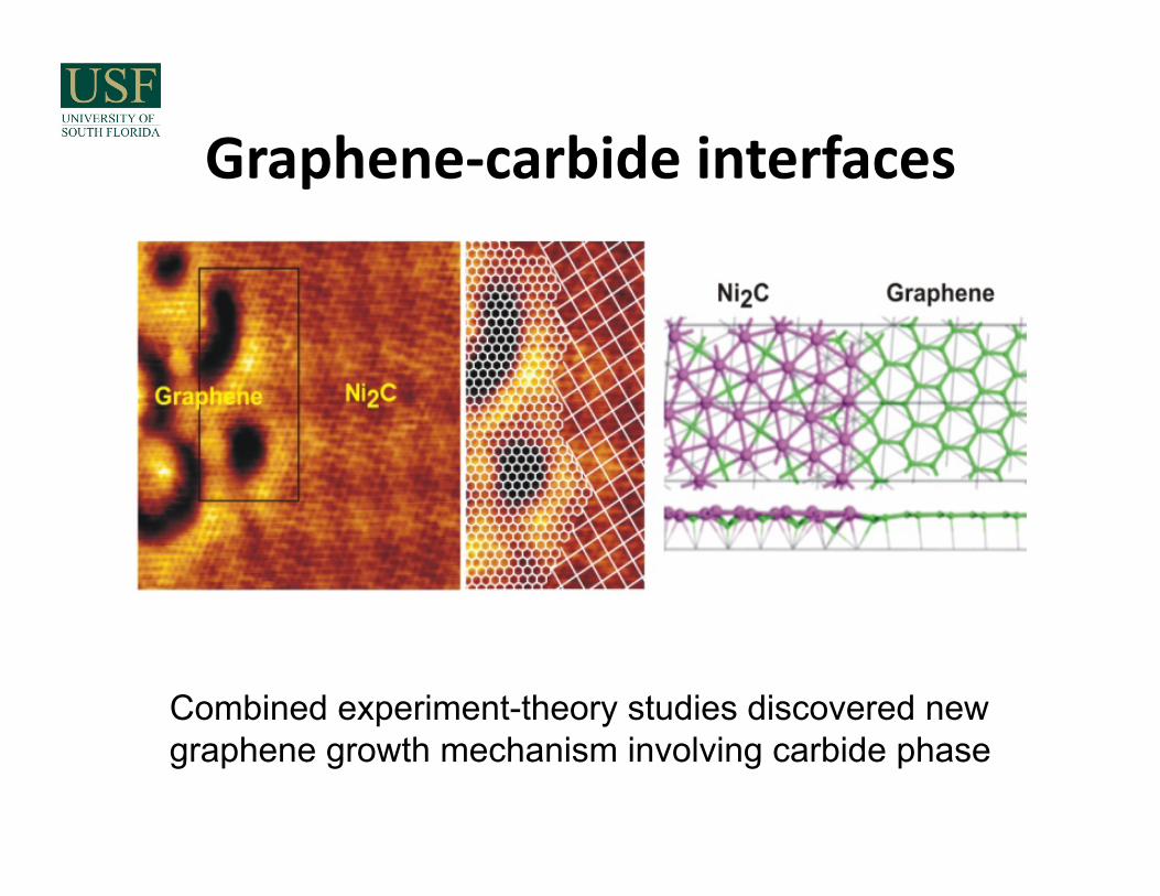
Graphene‐carbideinterfaces
Combined experiment-theory studies discovered new graphene growth mechanism involving carbide phase

Modelingofgraphenegrowthforsensingapplica'ons
• Growthmodel:kine4cMonte‐Carlo:topredictdefectstructuresasafunc4onofgrowthcondi4onsandeffectofsubstrate(Ni,Cu,NiCualloys)
• Needatomic‐scalemechanisms(MD)andreac4onrates(DFT)
• PreviousexperienceinmesoscaleKMCmodeling(seeexample–KMC/DFTmodelingofCVDdiamond)

Example:KMCmodelofdiamondgrowth
Method Variable time step kinetic Monte Carlo
Events are chosen based on their absolute rates
Reaction rates are determined from experiment/calculations
Growth rate on computer 1 mkm/h – same as in lab
But: critical input is needed from atomistic simulations regarding growth mechanisms and reaction rates

Diamond growth mechanism on (100) surface: quantum mechanical calculations of surface
chemistry ΔH, kcal/mol
# Gas phase
DFT (solid state)
1234
-6.6 -81.0 -8.0 -23.4
-8.7 -74.5 -18.8 -7.0
Hydrogen abstraction Methyle adsorption
2nd hydrogen abstraction Rate limiting step
Dimer opening

Reaction pathway of dimer insertion (β-scission)
Potential energy surface (PES)
R13
R23
3 1 2
R13
R23
Ea=13 kcal/mol
ΔH=-7 kcal/mol
Transition state
DFT predicts heat of dimer insertion reaction three times smaler than that obtained from cluster/MM calculations
Reactant
Product

Diamond growth on (100) surface: etching of CH2 adsorbate by atomic hydrogen
Inverse of dimer insertion H abstraction of CH2 moiety
Per site rate of etching:
From DFT calculations: ΔSI=6.4 cal/mol/K, ΔHI=+7.0 kcal/mol, GI=-0.7 kcal/mol
DFT predicts absolute rate of etching (per site): Retch=2*104 sec-1
4 orders of magnitude faster than that from gas-phase reaction set
Solution of puzzle for growth on (100) surface

KMC results with DFT reaction kinetics
Surface morphology of (100) film grown at 1200 K
Growth rates of (100), (110) and (111) films
Relative growth rates on (100), (110), (111) surface brought into agreement with experiment
KMC simulates smoth morphology on (100) surface in agreement with STM experiments

Conclusions
• Powerfulcombina4onofmaterialssimula4ontechniquesincludingdensityfunc4onaltheory,classicalmoleculardynamicsandmesoscalemodelingcombinedwiththeoryofcharge,spinandheattransportallowstoaIackabroadrangeofproblemsinmaterialsscience
• Exis4ngeffortinmodelingsensormaterialsandtheirsensorresponse
• Opentonewtheory‐experimentcollabora4onswithinFCASST

Materials Science & Engineering
Nino Research Group
Materials Development for EnergyMaterials Development for Energy--Related Applications andRelated Applications andInvestigation of StructureInvestigation of Structure--Property Relationships in Active CeramicsProperty Relationships in Active Ceramics
Dr. Juan Claudio NinoUF Research Foundation Professor
gg p y pp y p
Materials Science and Engineering, University of Florida 172 Rhines Hall, (352) 846-3787, [email protected]
Juan C. Nino – FCASST Sensors Kick-off Meeting – USF, Tampa, FL - December 2010

Materials Science & Engineering
Who we are…
Juan C. Nino – FCASST Sensors Kick-off Meeting – USF, Tampa, FL - December 2010 2

Materials Science & Engineering
Research Interests
PerformancePerformance
• Investigation of fundamental structure-property-processing-performance relationships in energy-related material systems and active ceramics
PerformancePerformance
?? ?
Synthesis &
Properties
Synthesis &
Properties
?
??Processing
Structure & Composition
Processing
Structure & Composition?
?
Id tifi d l ti hi ti l d i d d l t f d
CompositionComposition
Juan C. Nino – FCASST Sensors Kick-off Meeting – USF, Tampa, FL - December 2010
• Identified relationships rational design and development of new and improved materials with tailored properties for specific applications.
3

Materials Science & Engineering
Research StrategyS th i d P i P t P di ti d O ti i ti
0.00
0.25
0 50
0.75
1.00
Mol %
(Bi3/2
Zn1/2
)(Zn1/2
Nb3/2
)O7
Bi3/2
Zn1/2
Nb3/2
O13/2
(*) Bi
2Zn
2/3Nb
4/3O
7
BiNbO4
ZnNb2O
6
Mol %
1/2 Bi2O30.00
0.25
0 50
0.75
1.00
Mol %
(Bi3/2
Zn1/2
)(Zn1/2
Nb3/2
)O7
Bi3/2
Zn1/2
Nb3/2
O13/2
(*) Bi
2Zn
2/3Nb
4/3O
7
BiNbO4
ZnNb2O
6
Mol %
1/2 Bi2O3
0.4
0.6
0.8 BZN monoclinic
30 exp300
Ref
lect
ivity
0.08
0.10
0.12
0.14
Experimental Data J function fit
Synthesis and Processing Property Prediction and OptimizationAtomic/Ionic Response
PerformancePerformance
0.00 0.25 0.50 0.75 1.00
0.50
0.75
1.00 0.00
0.25
0.50
Mol %ZnO 1/2 Nb2O5
0.00 0.25 0.50 0.75 1.00
0.50
0.75
1.00 0.00
0.25
0.50
Mol %ZnO 1/2 Nb2O5
0 200 400 600 800 10000.0
0.2
Frequency (cm-1)
300 exp 300 fit 30 fit
0 50 100 150 200 250 3000.00
0.02
0.04
0.06
L0
tan
Temperature (K)
PerformancePerformance
?? ?
Material System Under Investigation
PhysicalUnderstandingof Phenomena
c
Synthesis &
Properties
Synthesis &
Properties
?
??
34
36 0.075
vity )
Under Investigation
Prototype Fabrication andCrystallographic Analysis
a
b
Processing
Structure & Composition
Processing
Structure & Composition?
?
24
26
28
30
32
34
0.015
0.030
0.045
0.060
Rel
ativ
e D
iele
ctric
Per
mitt
iv
Die
lect
ric L
oss
(tan
IncreasingFrequency
Prototype Fabrication and Performance Evaluation
CompositionComposition
100 150 200 250 300 350 400 450 50022 0.000
Temperature (K)
Juan C. Nino – FCASST Sensors Kick-off Meeting – USF, Tampa, FL - December 2010
Property CharacterizationMicrostructural Analysis
4

Materials Science & Engineering
Research CapabilitiesMaterials Synthesis
& ProcessingProperty
CharacterizationPerformance
I i C d ti itSolid-State ProcessingSolvothermalSol-gel synthesisCo-precipitation
Ionic ConductivityElectronic ConductivityGas Permeation Dielectric Permittivity(10 H 9 GH 10 1200 K)
Structure & C iti
p pElectrospinningDirect FoamingHeat Treatment (furnaces)• Microwave
(10 Hz – 9 GHz, 10 - 1200 K)Impedance SpectroscopyFerroelectric HysteresisPiezoelectric CoefficientsM ti P bilitComposition• Single Crystal
• Controlled Atmosphere• Quenching• Up to 1800°C
Magnetic PermeabilityBioactivity/Biomineralization
Juan C. Nino – FCASST Sensors Kick-off Meeting – USF, Tampa, FL - December 2010 5

Materials Science & Engineering
Research Capabilities
FEG-SEM
JEOL JSM-6335FJEOL TEM 2010FPhilips MRD X'Pert System
Crystallographic and microstructural characterization is performed at the Major Analytical Instrumentation
C ( C) C fCenter (MAIC) and Particle ERC at University of FloridaOver 40 characterization techniques including XRD, SEM, TEM, AFM, SPM, FIB XPS EDS WDS Auger FT-IR Raman Profilometry Ellipsometry
Juan C. Nino – FCASST Sensors Kick-off Meeting – USF, Tampa, FL - December 2010
FIB, XPS, EDS, WDS, Auger, FT IR, Raman, Profilometry, Ellipsometry, Nanoindentation, Light scattering (particle size), Mercury porosimetry, etc.
6

Materials Science & Engineering
Prototype Development & Demonstration
Research Capabilities - FISEPrototype Development & Demonstration Laboratory
Prototype capabilities for energyPrototype capabilities for energy conversion and energy efficiency device technologiesDirect Write Rapid Prototypingp yp g
Direct-write machine capable of dispensing ceramic/metallic inks and pastes, polymers, and biomaterials
S P i tScreen Printerlow-volume production using a fully automatic screen-printer
T C tTape CasterFabricates substrates for multilayer solid-state ionic devices, electronics
f fDedicated synthesis area and furnaces for pre- and post-processing.
Juan C. Nino – FCASST Sensors Kick-off Meeting – USF, Tampa, FL - December 2010 7

Materials Science & Engineering
Research StrategyS th i d P i P t P di ti d O ti i ti
0.00
0.25
0 50
0.75
1.00
Mol %
(Bi3/2
Zn1/2
)(Zn1/2
Nb3/2
)O7
Bi3/2
Zn1/2
Nb3/2
O13/2
(*) Bi
2Zn
2/3Nb
4/3O
7
BiNbO4
ZnNb2O
6
Mol %
1/2 Bi2O30.00
0.25
0 50
0.75
1.00
Mol %
(Bi3/2
Zn1/2
)(Zn1/2
Nb3/2
)O7
Bi3/2
Zn1/2
Nb3/2
O13/2
(*) Bi
2Zn
2/3Nb
4/3O
7
BiNbO4
ZnNb2O
6
Mol %
1/2 Bi2O3
0.4
0.6
0.8 BZN monoclinic
30 exp300
Ref
lect
ivity
0.08
0.10
0.12
0.14
Experimental Data J function fit
Synthesis and Processing Property Prediction and OptimizationAtomic/Ionic Response
0.00 0.25 0.50 0.75 1.00
0.50
0.75
1.00 0.00
0.25
0.50
Mol %ZnO 1/2 Nb2O5
0.00 0.25 0.50 0.75 1.00
0.50
0.75
1.00 0.00
0.25
0.50
Mol %ZnO 1/2 Nb2O5
0 200 400 600 800 10000.0
0.2
Frequency (cm-1)
300 exp 300 fit 30 fit
0 50 100 150 200 250 3000.00
0.02
0.04
0.06
L0
tan
Temperature (K)
Material System Under Investigation
PhysicalUnderstandingof Phenomena
c
34
36 0.075
vity )
Under Investigation
Prototype Fabrication andCrystallographic Analysis
a
b
24
26
28
30
32
34
0.015
0.030
0.045
0.060
Rel
ativ
e D
iele
ctric
Per
mitt
iv
Die
lect
ric L
oss
(tan
IncreasingFrequency
Prototype Fabrication and Performance Evaluation
100 150 200 250 300 350 400 450 50022 0.000
Temperature (K)
Juan C. Nino – FCASST Sensors Kick-off Meeting – USF, Tampa, FL - December 2010
Property CharacterizationMicrostructural Analysis
8

Materials Science & Engineering
Materials of InterestEl t i C i P l Bi i C itElectronic Ceramics – Polymers – Bioceramics – Composites
Research Topics
Electronics Fuel Cells Nuclear EnergyBioceramics Sensors
Dielectrics
Electronics Fuel Cells Nuclear EnergyBioceramics Sensors
Nuclear FuelsF l R iDielectrics
FerroelectricsThin Films
Piezoelectrics SOFC ElectrolytesPEM Membranes
Fuel Reprocessing
Thermoelectrics
Biocompatible fibersBioceramic Foams
Gamma Ray DetectorsPi i P l C it
PEM Membranes
Juan C. Nino – FCASST Sensors Kick-off Meeting – USF, Tampa, FL - December 2010 9
Bioceramic FoamsHyperthermia Cancer Treatment
Piezoceramic-Polymer CompositesSemiconductor Nanofibers

Materials Science & Engineering
Sensor-Related Activities
1. BiI3 Single Crystal Growth and Prototyping f G R D t tof Gamma-Ray Detectors
2. Piezoceramic-Epoxy Composites for Acoustic SensorsAcoustic Sensors
3. Semiconductor Nanofiber Synthesis via ElectrospinningElectrospinning
Juan C. Nino – FCASST Sensors Kick-off Meeting – USF, Tampa, FL - December 2010 10

Materials Science & Engineering
Gamma-Ray DetectorsBiI Crystals for High Energy Resolution Gamma Ray
Molecular pump
BiI3 Crystals for High Energy Resolution Gamma-Ray Spectroscopy (Funded by NNSA)
Mechanical pump
Vacuum systemVacuum system
Juan C. Nino – FCASST Sensors Kick-off Meeting – USF, Tampa, FL - December 2010
FurnaceBiI311

Materials Science & Engineering
Gamma Ray Detectors
10 oC/cm, 0.5 mm/h 10 oC/cm, 1 mm/h 15 oC/cm, 0.5 mm/h
40kLargest BiI single crystals ever
20k
25k
30k
35k
0012
009
006
ensi
ty (a
mu)
003
Largest BiI3 single crystals ever reported (18 x 13 x 5 mm3) have been successfully grown by modified vertical Bridgman method.
10 20 30 40 50 600
5k
10k
15k
0
Inte
BiI3 powder (10 mg/ml) BiI3 crystal (10 mg/ml)
Analyte Measured conc. (mg/l) Std. dev. Real conc.
(ppm) Measured
conc. (mg/l) Std. dev. Real conc. (ppm)
2 (degree)
113
Cu 3.167 0.2402 316.7 0.227 0.0264 22.7
Ag 0.015 0.0033 1.5 0.014 0.0003 1.4
Pb 0.511 0.0428 51.1 0.082 0.0018 8.2
Ni 0.008 0.0031 0.8 0.015 0.0056 1.5
Juan C. Nino – FCASST Sensors Kick-off Meeting – USF, Tampa, FL - December 2010
10 20 30 40 50 60Na 0.340 0.0916 34 0.55 0.1281 55
Si 1.230 0.1701 123 0.272 0.0412 27.2
12

Materials Science & Engineering
Gamma Ray Detectors
Sensor prototypes have been manufactured
• Au sputtered electrodes show the highest i ti it 2 109 (Ω )resistivity ~ 2 x 10⁹ (Ω·cm)
• Detectors fabricated with gold electrodes produced an observable 241Am alpha p pspectrum at room temperature.
2x10⁻⁶
Au)
0
1x10⁻⁶
u Pd Pt
ensi
ty (A
/cm
2 )
-2x10⁻⁶
-1x10⁻⁶
Cur
rent
De
Juan C. Nino – FCASST Sensors Kick-off Meeting – USF, Tampa, FL - December 2010 13
-400 -200 0 200 4002x10
Electric Field (V/cm)

Materials Science & Engineering
Sensor-Related Activities
1. BiI3 Single Crystal Growth and Prototyping f G R D t tof Gamma-Ray Detectors
2. Piezoceramic-Epoxy Composites for Acoustic SensorsAcoustic Sensors
3. Semiconductor Nanofiber Synthesis via ElectrospinningElectrospinning
Juan C. Nino – FCASST Sensors Kick-off Meeting – USF, Tampa, FL - December 2010 14

Materials Science & Engineering
Piezoceramic-Epoxy Composites
We are utilizing an in-situ polymerization process that results in a dense strutresults in a dense strut mesostructure and controllable ceramic microstructure.
The ceramic foams have been infiltrated with an epoxy to form p ya 3-3 piezoelectric composite with acoustic impedance matching suitable for
Juan C. Nino – FCASST Sensors Kick-off Meeting – USF, Tampa, FL - December 2010 15
matching suitable for sonar/sensing applications.

Materials Science & Engineering
Sensor-Related Activities
1. BiI3 Single Crystal Growth and Prototyping f G R D t tof Gamma-Ray Detectors
2. Piezoceramic-Epoxy Composites for Acoustic SensorsAcoustic Sensors
3. Semiconductor Nanofiber Synthesis via ElectrospinningElectrospinning
Juan C. Nino – FCASST Sensors Kick-off Meeting – USF, Tampa, FL - December 2010 16

Materials Science & Engineering
Nanofiber Synthesis
Electrospinning of insulating and semiconducting nanofibersSyringe Pump
BaTiO3Syringe
PrecursorSolutionNeedle
HV PowerSupply
3
MovableJack
E-spunFiber
We are investigating the nucleation and growth process
Electrospinning is an extremely versatile method that enables the
50 nm50 nm
growth process through controlled annealing to obtain single crystalline
synthesis and collection of continuous nanofibers of
polymers, ceramics and their
Juan C. Nino – FCASST Sensors Kick-off Meeting – USF, Tampa, FL - December 2010
single crystalline nanofiberscomposites.
JACS, 89 [2] 395–407 (2006)
17

Materials Science & Engineering
Nino Research Group
Materials Development for EnergyMaterials Development for Energy--Related Applications andRelated Applications andInvestigation of StructureInvestigation of Structure--Property Relationships in Active CeramicsProperty Relationships in Active Ceramics
Dr. Juan Claudio NinoUF Research Foundation Professor
gg p y pp y p
Materials Science and Engineering, University of Florida 172 Rhines Hall, (352) 846-3787, [email protected]
Juan C. Nino – FCASST Sensors Kick-off Meeting – USF, Tampa, FL - December 2010

Biopolymer-basedfunctional materialsin medicine and biotechnology
Don Haynie
First FCASST meetingTampa9 December 2010

New Florida Outcomes for 2015
Increased annual patent awards Medical breakthroughs that improve the
longevity and quality of life Increased annual new business start-ups
BioLaminex

What we do Basic/applied, peptides, medicine,
biotechnology, nanoscale
Peptide-based electrospun fibers Structure and function of a tumor
suppressor Peptide-based multilayer films Synthetic vaccines Coatings for implant devices Coatings for in vitro cell culture

Biosensors
Sensitive bio-active element Transducer Electronics

Multilayer films
Coulomb’s law2nd law of thermodynamics
F = kq1q2/r2
∆S ≥ q/T
Polymer self-assembly driven by:
Positivepeptide
Buffer/water
Negativepeptide
Buffer/water
Positivepeptide
Buffer/water
Negativepeptide
Buffer/water
++
++++
++
+++
++
++
++
++++
++
+++
++
++
−−
−
−
− −−
−
−
− −−
−
−
−
Planar support
Spherical support

Characterization
15 20 25 30 35 400
20
40
60
80
4 6 8 10 12 14 16 18 2002468
10121416182022
Thi
ckne
ss, n
m
Adsorption step
pH 7.4 pH 7.8 pH 8.9
Thi
ckne
ss, n
m
Adsorption step
Thic
knes
s, nm
Adsorption step
Adsorption step
Abs
orpt
ion
at 2
77 n
mβ sheet
Hei
ght (
nm)

Synthetic vaccines
Nanoparticles designed to interact with immune system
Continue in design loop until formulation Passes various in vitro tests (e.g.
biocompatibility) Confers immunity on test organisms
Applications: vaccines
ENTER EXIT
CELL ARTIFICIAL TECHNOLOGIES, INC. Commercializing Polypeptide NanoEngineering for Medicine and Industry

Example
Reducingenvironment
Oxidizingenvironment
Acidicenvironment
Crosslinks No crosslinks
Outside cell Inside cell Inside lysosome
Functionalize particle surface with peptides for specific targeting and specific effects on the immune system

Coatings for implant devices
Nanofilms designed to interact with tissues
Continue in design loop until formulation Passes various in vitro tests Confers increase in implant utility in vivo
Applications: glucose sensor implant

Coatings for in vitro cell culture
Nanofilms designed to interact with cells Continue in design loop until formulation Confers desired level of control over cell
behavior
Toxicity testing, drug discovery, biocompatibility, cell screening BioLaminex

Past and present funding sources
NIH NSF DOE AFOSR Medical Research Council Nuffield Foundation Royal Society Others

Expertise
Biophysics Selected methods of
micro/nanofabrication Biomaterials design, characterization and
development Biological macromolecule structure,
function and thermostability

Simulation of Ionic Transport and S f R ti fSurface Reactions for
Electrochemical Systemsy
Simon Phillpot and Susan SinnottD t t f M t i l S i d E i iDepartment of Materials Science and Engineering
University of FloridaDecember 9 2010ece be 9 0 0

Anatomy of an SOFC
http://www.doitpoms.ac.uk/tlplib/fuel-cells/high_temp_sofc.php?printable=1
SEM micrographs of the cross section of: (a) fractured cell; (b) part of anode; (c) double-layer cathode
d (d) th t i f YSZand (d) the top view of YSZ electrolyte ).
Y.J. Leng et al. / International Journal of Hydrogen Energy 29 (2004) 1025 – 1033

-Bi2O3H Inaba et al Solid State Ionics 83 1 (1996)H. Inaba et al. Solid State Ionics, 83 1 (1996)
•Fluorite phase is unstable at 500°C
Bi O
VOp•Dopants are added to stabilize at the cost of ionic conductivity

Stabilization of Bi2O3 using Dopants
Sammes et al. J. Eur. Ceram. Soc. 19, 1801 (1999)Wachsman et al. Ionics 7, 1 (2001)

Cation Polarizability is ImportantO l O P l i bl O l Bi P l i blOnly O Polarizable Only Bi Polarizable
What shuts down the diffusion in Bi2O3?diffusion in Bi2O3?

Why is Polarizability Important
Examine Oxygen Diffusion
Bi Bi
Examine Oxygen Diffusion
What is the structure of the
hsystem when diffusion shuts down?

Oxygen adsorption at cathode
O2O2 + 4e- 2O2-
Bulk and grainBulk and grain boundary diffusion
Surface diffusion
Three-phase boundary
Electrolyte
Three phase boundary
La1-xSrxCoyFe1-yO3- (LSCF) LaFeO3 http://www.americanelements.com/lscf.html

Surface Stability: Thermodynamic Calculations
3LaFeO bulk La Fe OE 3 2OE
x y 2
0 0f , M O OH ,S
(T , P )La or Fe
vapor
2o (T , P )La or Fe
Surface slab
:from DFT:from Exp
Range of μLa or μFefor stable bulk LaFeO3
A 0
:from Exp.Etot of La, Fe, La2O3, FeO, Fe2O3, and Fe3O4

Surface Phase DiagramV) P(O )
Stable region for bulk LFOE O
2) (e
V
: Stable region for bulk LaFeO3
T
1010
800K
1000K
P(O2)
for bulk LFO
μ O-1
/2
T
1101
0.21
1000K
μO
(=
10-10
P(O2)
μ (=μ E )(eV)
10-2010-30
10-4010-5010-60
μLa (=μLa-ELa)(eV) T (K)

CO2 Reduction: Role of SurfacesZnO(10 10) Cu term Cu term –ZnO(10‐10) Cu term –
Cu2O(100)Cu2O(111)
Using DFT to examine reaction mechanisms for CO2 reduction to methanol and l t id th ( th )relevant side paths (e.g. methane) Surfaces are initially chosen based on experimental results Examining both a vacuum and electrochemical environment
Pathways for activation for C-O bond in CO2CO2(g) CO2 (a)CO2(a) CO(a) + O(a)CO (a) + H(a) OCOH(a) OC(a) + OH(a) (hydrogen assisted C O activation)CO2(a) + H(a) OCOH(a) OC(a) + OH(a) (hydrogen assisted C-O activation)
How are the reaction steps changed based on the surface? Can we promote/suppress certain reaction steps by the choice of surface structure?

Adaptive KMC: Processp
Find all saddle points usingthe dimer transition searchingthe dimer transition searching
method
)exp(Tk
Evr A
j
Determine the rate for each transition
)p(TkB
j
Kf : rate for successful escapev : average frequencyv : average frequencyEA : activation energy

Adaptive KMC Test Application: Diffusion of an Al adatom on the Al (111) surfacean Al adatom on the Al (111) surface
State A Saddle State BE = 0 eV E = 0 23 eV E = 0 eV
Initial structureEA= 0 eV Ea= 0.23 eV EB= 0 eV
PBC
Al atom
y
z
x y6 layered Al (111) surface

Parameterizing Hydrocarbon-Cu-ZrO2-TiO2PotentialPotential
• Cu-Cu2O-TiO2 COMB potential complete and the results are being p gwritten up
• Adding hydrocarbons to the COMBAdding hydrocarbons to the COMB potential is in progress

Infrared Sensors : Toward SWIR Infrared Sensors : Toward SWIR WavelengthsWavelengthsgg
Franky SoDepartment of Materials Science andDepartment of Materials Science and
Engineering
University of Florida

Research areas
• Organic light emitting diodesOrganic light emitting diodes• Polymer solar cells
I f d• Infrared sensors• Quantum dot devices• Device physics

Using Nanocrystals for IR detection
5
PbSe and PbS
2
3
4
orpt
ion
(a.u
.)
600 800 1000 1200 1400 1600 18000
1Abs
o
W l th ( )Wavelength (nm)
CdSe

Limitations of Colloidal Nanocrystals
• Limitations– Long capping groups– Surface dangling bonds
NC– Stability
• What can be done?
NC
What can be done?

Solving the Problem: modify the process
(oleic acid)Synthesis
Washing
(octylamine)
TolueneChlorobenzeneChloroform
Washing
Spincoating
Multiple cycles(Benzenedithiol) Multiple cycles
(Ethanedithiol)
Ligand Exchange

Ethanedithiol BenzenedithiolUntreated
Better Film Morphologyci
dO
leic
ac
R= 5.02nm R= 1.90nmR= 1.50nm
amin
eO
ctyl
a
R= 1.62nm R= 1.55nmR= 1.51nm

Photodetector IV Characteristics
Why is there not rectification?
CB CB
shallow traps
cathodeC C
Dithiol
anode VB VB
Devices with high density of mid gap
mid-gap traps
Devices with high density of mid-gapstates may be experiencing charge tunnelingChemistry of Materials 22, 3496 (2010)

Temperature Dependence
Dithiol treated Not treated with dithiols
Chemistry of Materials 22, 3496 (2010)

Double heterostructure to reduce dark current
Adv. Funct. Mater. 2010

Designing the device structure
C60
Poly-TPD
TFB

Dark Current Reduction
Dark Currents
Adv. Funct. Mater. 2010

DetectivityDetectivity:
2/12/1 )2(
/
)2(*
d
lightph
d qJ
LJ
qJ
RD
Noise equivalent power:
NEP */)( 2/1 DfA)()( dd qq
Adv. Funct. Mater. 2010

Nanophysics and Surface Science LaboratoryMatthias Batzill, Dept. Physics, USF, p y ,
Oxide Surfaces Graphene
Surface Structure- Property
RelationshipPhoto Catalysis Atomic-scale
Defect structuresBasic Science of
graphene formationRelat onsh p
Funding: Funding:
CAREER: Nanoscale surface properties of functional metal oxides
Graphene defects and their engineering for nanoelectronics applicationsf m
Photocatalysis of modified transitionmetal oxide surfaces
nanoelectronics applications
Collaborative Research: Experimental and theoretical study on the structure and catalytic activity of metal cluster/metal oxide interfaces

What are our experimental capabilities? Atomic scale surface analysis Chemical surface analysistom c scale surface analys s
UHV Chamber equipped with:Scanning tunneling
hem cal surface analys sUHV Chamber equipped with:Temperature programmed desorption tunneling
microscope (STM)Low energy electron diffraction ( EE )
(TPD)Low energy electron diffraction (LEED)Auger electron
Ultrahigh vacuum (UHV) surface analytical and
l ti
(LEED)
Ch i l d l t i
Auger electron spectroscopy (AES)
sample preparationmethods
Chemical and electronic structure by photoemission
UHV Chamber equipped with:X-ray h i i
Thin film growth of oxidesby pulsed laser deposition
UHV Chamber equipped with:Reflection high photoemission
spectroscopy (XPS) UV-photoemission spectroscopy
Reflection high energy electron diffraction (RHEED) and in-situ sample spectroscopy
(UPS) transfer to photoemission chamber

How can our research contribute to sensors? •Surface/interface properties are critical for chemical sensing Surface/interface properties are critical for chemical sensing.
•Our Lab is ideally situated between applied sensors and computational studies to investigate fundamental properties of molecule surface i iinteractions.
• We can use our material preparation and characterization methods to develop atomic scale modified surfaces to tune molecular adsorption.develop atomic scale modified surfaces to tune molecular adsorption.
On the next few slides we are presenting recent studies in the Nanophysics and Surface Science Lab that can be easily leveraged for chemical sensing applications.

1. Dependence of molecular adsorption on crystal structure, e.g. acetic acid adsorption on rutile TiO2 (110) vs. TiO2(011)-2x1.
TiO2(110) TiO2(011)-2x1
=>Acetic acid adsorbs homogenously in an ordered overlayer, with a small barrier for adsorption
=>Acetic acid adsorbs heterogenously in clusters with a kinetic barrier for adsorption.
adsorption
=> Strong surface dependence for adsorption will enable tuning of gas responses on well-defined surfaces

2. Role of surface structure on electronic properties.
Comparison of the atomic structure of TiO2(011)-2x1 and (110) surfaces. The reconstruction of the (011) surfaces places the Ti-cations in a distorted square pyramidal co-ordination environment This (011) surfaces places the Ti cations in a distorted square pyramidal co ordination environment. This causes a varied crystal-field compared to the regular octahedral structure of TiO2. Consequently, excess electrons on these sites exhibit a different binding energy as is measured by UPS shown on the right.
R d M Read More: J. Tao, M. Batzill “Role of Surface Structure on the Charge Trapping in TiO2 Photocatalysts” J. Phys. Chem. Lett. 1, 3200-3206 (2010).

3. Use of novel sample preparation methods for tuning molecule-surface interactions, e.g. grazing incidence low energy ion sputtering to create adsorption sites (under coordinated step edge sites).p ( p g )
Use of grazing incidence low energy ion beams for creating stepped surfaces by
Atomic scale structure of meta-stable step edge orientation. Comparison between experiment (c) and computational (d) STM
g pp ypreferential step edge erosion. experiment (c) and computational (d) STM
image=> Method for nanopatterning oxide surfaces with active sites for gas adsorption and detectionRead More:T Luttrell M Batzill "Nanoripple formation on TiO2(110) by low-energy grazing incidence ion T. Luttrell, M.Batzill Nanoripple formation on TiO2(110) by low energy grazing incidence ion sputtering" Physical Review B 82, 035408 (2010).
T. Luttrell, W.K. Li, X. Gong, M. Batzill "New Directions for Atomic Steps: Step Alignment by Grazing Incident Ion Beams on TiO2(110)",, Physical Review Letters 102, 166103 (2009).

4. Direct investigations of surface modifications due to the interaction with the gas phase, e.g. ZnO with H2S => formation of monolayer ZnS.
(a) Photoemission studies of variation of valence band with increasing exposure increasing exposure to H2S.
(b) Work function, band bending, and valence band maximum h f i
STM images of monolayer ZnSformation by exposure of ZnO to H2S
change as a function of surface sulfur concentration.
formation by exposure of ZnO to H2S
Read More:"Surface Functionalization of ZnO Photocatalysts with Monolayer ZnS" J Lahiri and M Batzill J
=> Surface science studies can elucidate all important surface changes during gas sensing reactions.
Surface Functionalization of ZnO Photocatalysts with Monolayer ZnS J. Lahiri and M. Batzill J. Phys. Chem. C 112, 4304 (2008).
“Soft x-ray photoemission of clean and sulfur-covered polar ZnO surfaces: A view of the stabilization of polar oxide surfaces" J. Lahiri, S. Senanayake, and M. Batzill, Phys. Rev. B 78, 155414 (2008).

5. Atomic scale defects in graphene as active sites for molecular adsorption.
Atomic scale domain boundaries in graphene can be designed using a metal substrate as template. These one dimensional defects have exciting properties that may also affect gas adsorption and subsequently the conduction through these atomic wires. This can be used for ‘futuristic’ single
Read More:"Graphene destruction by metal carbide formation: An approach for patterning metal-supported
h "J L hi i d M B t ill A li d Ph i L tt 97 023102 (2010)
subsequently the conduction through these atomic wires. This can be used for futuristic single molecule detection.
graphene"J. Lahiri and M. Batzill Applied Physics Letters 97, 023102 (2010).
"An extended defect in graphene as a metallic wire” J. Lahiri, Y. Lin , P. Bozkurt , I. Oleynik and M. Batzill Nature Nanotechnology 5, 326 - 329 (2010).

Trace Gas Sensing Enhanced by Cavity Quantum Electrodynamics
Andreas Muller, USF physics

Cavity Quantum Electrodynamics
Cavity QED: the electromagnetic field in the cavity is quantized and the density of states available for emission isquantized, and the density of states available for emission is modified. Consequently, light emission by a test gas can be increased by orders of magnitude compared to free space.
Advantages of micro cavity:g y• High vacuum field (small mode volume)• High laser intensity (small• High laser intensity (small beam waist)• High stability• Small footprint

Micromirror Technology
CO2 laser ablation:Produces ultra smooth surfaces for high reflectivity coatings R> 99.99%
A. Muller et al., Optics Lett. 35, 2293 (2010).

Gas Sensing
Raman scattering IR fluorescenceMethod:
Theo Enhance
Requirements: Spectral bandwidth of transitions < 10 GHz:
Theo. Enhance. over free space
Challenges: Fab micromirrors atCreate double
~106‐107
Challenges: Fab. micromirrors at ~4.5 m & laser+Det
Create double resonance condition
Goal: detection of atmospheric gases (CO2, …), chemical warfare agents (Mustard‐gas, Phosgene,
l i d ) i ppb ppmexplosive compounds, …) in ppb‐ppm range

Nanostructure Optoelectronics LabNanostructure Optoelectronics LabDr. Xiaomei Jiang
Research FocusBasic studies of material properties, device physics and device engineering Fabrication and characterization of nanostructure photonic and electronic devices (solar cells, light emitting diodes and thin film transistors)
Research ProjectsDevelopment of Semitransparent Flexible Power Foil for Smart Window Technology, sponsored by New Energy Solar Corporation and Florida High Tech Corridor FundsNanocomposite of Infrared Quantum Dots and Conducting Polymers: Possible Multiple Exciton Dissociation, sponsored by ACS PRF grant Microstructure organic solar arrays for MEMS devices, sponsored by USF in the direction of Functional Multiscale Materials by Design (FMMD)
Organic Solar ModuleOrganic Solar Module
Plastic Solar CellPlastic Solar Cell
Excitons and charges in quantum dots solar cell

1. Semitransparent Flexible Power Semitransparent Flexible Power Foil for Smart Window TechnologyFoil for Smart Window Technology
In this project, we aim at the production of a prototype 1ft by 1 ft solar window, either in form of direct coating onto window glass, or as a stand-alone flexible ‘power foil’ which can be easily installed on existing windows. The objective is to modify the current complicated and costly processing techniques such as vacuum deposition, area-limited spin-coating process, and photolithography, environments. The technical approaches while maintaining the device performance in field application include creation of transparent contacts, development of a scalable solution processable technology for large scale manufacturing, and optimization of device performance.

See though SolarWindowTMSee though SolarWindowTM

SolarWindowTM on a model houseSolarWindowTM on a model house

2. Hybrid Quantum Dots Solar Cells2. Hybrid Quantum Dots Solar Cells
We propose to study possible multiple exciton dissociation in the nanocomposite of conducting polymer/infrared quantum dots. We are going to further optimize band alignments between polymer and quantum dots by using various polymers of reduced bandgaps with different sizes of infrared quantum dots; to improve quantum dots transport properties by controlling surface states via post synthesis ligand-exchange and thermal annealing.
The anticipated outcome of this project will cast insight in understanding the new physics governing multiple carrier process, which is of great importance for basic research in the area of solar energy utilization.

Quantum Dots Solar Cells
Hybrid solar cells based on nanocomposite of PbS QDs/RRP3HT
S
S
S
S
RRP3HT

Possible Indication of Multiple Carrier Extraction
P3HT
PbSe NCe
h
P3HT
PbSe NC
2e2h
0.5 1.0 1.5 2.0 2.5 3.0 3.50
2
4
6
8
10
12
14
0.5 1.0 1.5 2.0 2.5 3.0 3.5 4.0 4.50.0
0.1
0.2
0.3
0.4
(a)
IQE
(%)
Energy (eV)
P3HTwith PbSe QD
5nm7nm8nm
Ab
sorp
tio
n(a
.u.)
Energy (eV)
(b)
(c)
Fig.1. (a) Internal quantum efficiency (IQE) of three P3HT/PbSe photovoltaic devices with different sizes of PbSe QDs. The straight line was to guide the eyes for the rapid increase of IQE at higher photon energy. The inset shows absorption spectra of hybrid composite films (symbols). The black line presents the absorption of neat P3HT. (b) Single electron transfer upon absorption of infrared photon; (c) conjecture of two holes transferred to P3HT from QD upon absorption of > 3 Eg photon.

3. Microstructure organic solar arrays for MEMS devices
In this project, we design an organic microarray as reference power supply for an ultra-high-Q and ultra-high-frequency (UHF) extensional-mode resonant mass sensors with distinctive binding sites for targeted species, microfabricated with functional multiscale materials, as a portable platform for biological/chemical molecular assays (Fig. 2). The proposed research nicely leverages the existing research strength of the two colleges and will spur new vigor for a myriad of new application in the future. The proposed project is expected to lead to significant economic development and industrial interaction.

Research DirectionsResearch Directions
Generation III solar cells aim at both high efficiency and low cost, I propose two main approaches toward fulfillment of cost-effective solar cells:1). Organic multi-junction (tandem) photovoltaic devices
I propose to implement the large-scale solution processable technology developed in my lab to tandem organic photovoltaic devices. This research aims on solving the following challenges:(a) Spectra mismatch between material absorption and solar spectrum(b) Exciton diffusion ‘bottleneck’(c) Carrier loss due to recombination from front and back cells (d) Large contact resistance
1. Generation III cost-effective photovoltaic technology

2). Organic/inorganic hybrid solar cells
To study photoinduced charge transfer (PCT) process separately from the free carrier transport (FCT) is an important first step to guide the interface engineering for high efficiency hybrid quantum dots solar cell, yet the current research effort is missing this important first step. We propose a systematic study about PCT in NCs composites with different interfacial environments, and a sequential investigation of FCT within these composites. The goal of the proposed research is to deepen our understanding, and suggest design optimization of nanocrystal/polymer composites, including ideas for new polymers that match these material systems for potential high efficiency solution processable photovoltaic devices.

2. Fundamental research on optoelectronic properties of new materials
1) to study optical properties of materials mainly by Continuous Wave Photoinduced Absorption (cw-PA) (also being called pump & probe or photomodulation spectroscopy (Fig.3)).
Monochrometer
Lock-inamplifier
Probe light (200nm to 5 m)
Pump laser(488 nm)
DetectorSample
Cryostat (10K)
computer
Focus lens
pump h g,op
probe
•create long-lived excitations with modulated laser-pump• record changes in the probe absorption spectrumusing phase-sensitive technique (Lock-in amplifier)
Measure: d=-T/T nedne: density of photoexcitationsoptical cross-sectiond: sample thickness
Also capable of measuring:•lifetime of photoexcitation•Activation energy of gap state•Recombination kinetics of photoexcitations

2) The study of transport properties of semiconductors is by Transient and steady transport spectroscopy (Fig. 4). The main techniques are Time of Flight (TOF) and Carrier Extraction by linearly Increased Voltage (CELIV), which are complimentary in nature.
Glass/ITO/Active film/AL
Digital oscilloscope
TOF
CELIV
Pulse laserExtract holes
Pulse laserExtract electronst
t
Major functions of TOF and CELIV: •Measure carrier mobility and Identify carrier transport type (i.e., dispersive or non-dispersive) •Determine the type of loss mechanisms, i.e., is it the diffusion controlled bimolecular recombination (Langevin recombination), or monomolecular recombination

Selected Publications
• Fundamental study
• Applications
1. J. Lewis, S. Wu and X. Jiang, Unconventional gap state of trapped exciton in PbS quantum dots, Nanotechnology 21, 455402 (2010).
2. X. Jiang, R. Österbacka, and Z. V. Vardeny (2008). Optical and Transport Studies of Poly (3-hexylthiophene); Nanomorphology Dependence, Encyclopedia of Nanoscience and Nanotechnology (second edition), American Scientific Publishers, publication in process. (2010)
3. J. Zhang and X. Jiang, Confinement-dependent below-gap state in PbS Quantum Dots Films probed by cw Photoinduced Absorption, Journal of Phys. Chem. B letters 112, 9557–9560(2008).
4. J. Zhang, X. Jiang, Steady State Photoinduced Absorption of PbS Quantum Dots Film, Appl. Phys. Lett. 92, 14118 (2008).
1. J. Lewis, J. Zhang and X. Jiang, Over 30% transparency inverted organic solar array by spray, in print (2010).
2. J. Lewis, J. Zhang and X. Jiang, Fabrication of organic solar array for applications in microelectromechanical systems, Journal of Renewable and Sustainable Energy 1, Vol. 1 (2009).
3. X. Jiang, R.D. Schaller, S.B. Lee, J.M. Pietryga, V.I. Klimov and A.A. Zakhidov (2007). PbSe Nanocrystal/Conducting Polymer Solar Cells with 2 Microns Infrared Response, Journal of Material Research 22, No. 8, 2204-2210.
4. G. Dedigamuwa, J. Lewis, J. Zhang, X. Jiang, P. Mukherjee and S. Witanachchi, A laser-assisted spray process for the growth of surfactant-free PbSe quantum dot films, Appl Phys Lett 95, 122107, (2009).

Organic deposition system(integrated vacuum chamber, thin film coating glove box systems)
Lab Facilities

•Current-voltage (I-V) curve (power conversion efficiency)•Spectral sensitivity (external quantum efficiency)
Solar cell characterization

cw pump & probe spectroscopy (UV, visible &Infrared)

Transient transport spectroscopy set up

The GroupThe Group
Jason, Ph.D candidate
Evan, Ph.D student Patrick,
undergraduate student
Dr. Thapa, postdoc