Embed Size (px)
Citation preview

ELcon Consulting & Engineering
Brunnhaldenstrasse 8 3510 Konolfingen Switzerland
Telefon Fax E-Mail Shop
+41 (0) 31 792 04 61 +41 (0) 31 792 04 62 [email protected] http://shop.elcon.ch
EL-34 FLL-VFO Stabilizer
for transceivers without PLL or DDS frequency conditioning
e.g. Yaesu FT-101, Heathkit SB-104 etc.
Building and functional description
Version 2.0b, only from firmware V2.0b-20200725
20. September 2020

EL-34_V2.0c_en.docx September 20, 2020, © Elcon, Switzerland Page2 / 28
Table of contents
1 Introductory remarks ....................................................................................................................... 3
2 How it works .................................................................................................................................... 3
2.1 The Frequency Locked Loop (FLL) ........................................................................................ 3
3 Assembly of the module .................................................................................................................. 6
3.1 Parts list .................................................................................................................................. 7
3.2 Mounting the circuit board ...................................................................................................... 9
4 Function test of the board ............................................................................................................... 9
4.1 Power up test ....................................................................................................................... 10
4.2 RF test .................................................................................................................................. 10
5 Installations ................................................................................................................................... 12
5.1 Connector Assembly ............................................................................................................ 12
5.2 RF Signal from Transceiver VFO ......................................................................................... 13
5.3 VFO tuning circuit ................................................................................................................. 13
5.4 Using the CLARIFIER circuit ................................................................................................ 15
5.4.1 Clarifier Resistor Rx and VRef ............................................................................................ 15
5.5 Assembling the module into the transceiver ........................................................................ 17
6 Operation ...................................................................................................................................... 18
6.1 Delay after tuning ................................................................................................................. 18
6.2 Status display ....................................................................................................................... 18
7 Programming via USB to Serial Adapter ...................................................................................... 19
7.1 Connection to FLL VFO Stabilizer ........................................................................................ 19
7.2 Entering commands ............................................................................................................. 21
7.3 Commands ........................................................................................................................... 22
7.3.1 H Help .............................................................................................................................. 22
7.3.2 SAVE SAVE ..................................................................................................................... 22
7.3.3 ULD ULDELAY "n" ........................................................................................................... 22
7.3.4 ULF ULFREQ "n" ............................................................................................................. 23
7.3.5 VE VERSION ................................................................................................................... 23
7.3.6 VR VREF"n" ..................................................................................................................... 23
7.3.7 VREFC VREFCOR ON/OFF ............................................................................................ 25
8 Appendix ....................................................................................................................................... 26
8.1 Specifications ....................................................................................................................... 26
8.2 Ruler ..................................................................................................................................... 26
8.3 Repair / Warranty ................................................................................................................. 26
8.4 Disclaimer of liability ............................................................................................................. 27
8.5 Schematic ............................................................................................................................. 28
8.6 Circuit board assembly ......................................................................................................... 28
Important! Hints or tips for the correct function of the EL-34.
Watch it! Absolutely observe.

EL-34_V2.0c_en.docx September 20, 2020, © Elcon, Switzerland Page3 / 28
1 Introductory remarks
Many radio amateurs still use older radios which do not have a modern frequency synthe-sizer. Today's digital operating modes, however, require a frequency stability that only mod-ern transceivers can provide.
Usually a free-oscillating oscillator (VFO, Variable Frequency Oscillator) is the reason for the large frequency drift. The reason can be the insufficient voltage stabilization for the VFO, but mostly the fluctuating temperature is the reason for the drift of several 100 Hz.
The EL-34 module has been developed for all radios with free-running VFO and can be built into various transceivers.
2 How it works
The slow running away of the frequency is called frequency drift. With the help of tempera-ture-controlled crystal oscillators (TCXO) or by installing a crystal in thermostats (oven-con-trolled crystal oscillator, OCXO) it is possible to build extraordinarily long-term stable oscilla-tors.
Unfortunately, the performance of many VFOs of older devices does not match the perfor-mance of modern DDS oscillators in today's commercial amateur radios. We cannot rede-velop the entire transceiver, but want to make the frequency stability of the VFO crystal stable with a relatively simple additional circuit.
The development of a frequency-stable VFO is difficult, because even an output power of more than 1mW generates so much heat in the transistors that it supports the frequency drift in the long run.
The reasons for the frequency drift are different. The temperature has a particularly strong ef-fect on the capacitance diode, which is used for the "Clarifier" function, and thus on the stabil-ity factor of the entire oscillator. A temperature change changes the diode capacitance as well as the bias voltage of these diodes. The junction temperature changes, resulting in drift.
As you will see, this capacitance diode is not only bad, but with our VFO stabilization it changes into a useful component.
2.1 The Frequency Locked Loop (FLL)
A Frequency Locked Loop (FLL) is an electronic control system that generates a signal set to the frequency of an input or reference signal. This circuit compares the frequency of a con-trolled oscillator with the reference and automatically increases or decreases the frequency of the oscillator until its frequency (but not necessarily its phase) matches that of the reference.
Such circuits are used as frequency doublers, for FM demodulation and for stabilizing RC os-cillators.
With this circuit technology we want to stabilize our strongly drifting VFO.

EL-34_V2.0c_en.docx September 20, 2020, © Elcon, Switzerland Page4 / 28
The block diagram of the FLL is shown in Figure 1.
Figure 1
The circuit has a negative feedback loop that acts on the VFO. For frequency correction, the capacitance diode built into the VFO (primary for CLARIFIER) is also used.
The input signal of the FLL is the VFO frequency. The prescaler only serves to generate a symmetrical square wave signal that can be processed with a modern microcontroller. This frequency signal is compared with the identical but
delayt delayed signal. The comparator gen-
erates a correction signal which then controls the frequency of the VFO via a low-pass filter. Since the signals are averaged over complete cycles, the output of the FLL is phase-inde-pendent.
The FLL engages with everyone lockup point VFO stepf n f . This has the advantage that the
FLL immediately stabilizes the VFO after the VFO tuning knob is no longer turned.
Figure 2
If e.g. and 0.2delayt s amount 2N , then the FLL step size will 10stepf Hz be. Mathematically
derived, the lockup point can be calculated as follows:
step
delay
Nf
t
A derivation is left to the reader as an exercise.
The snap-in step frequency is independent of the FLL input frequency and therefore constant over the entire VFO range.
The FLL is very fast compared to a PLL circuit (Phase Locked Loop), because not the phase but the frequency is corrected.
VFO
CLARIFIER
Tuning diode
5-5.5MHzPrescaler
N
Delay-Linetdelay
ComparatorLow-pass
Filter
Frequency Locked Loop (FLL)
0f 0 stepf f0 3 stepf f0 2 stepf f
0 stepf f
Tuni
ng-V
olta
ge
EL-34_V2.0c_en.docx September 20, 2020, © Elcon, Switzerland Page5 / 28
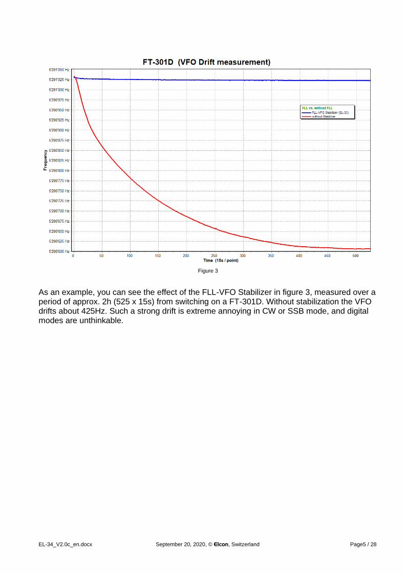
Figure 3
As an example, you can see the effect of the FLL-VFO Stabilizer in figure 3, measured over a period of approx. 2h (525 x 15s) from switching on a FT-301D. Without stabilization the VFO drifts about 425Hz. Such a strong drift is extreme annoying in CW or SSB mode, and digital modes are unthinkable.

EL-34_V2.0c_en.docx September 20, 2020, © Elcon, Switzerland Page6 / 28
3 Assembly of the module
For the assembly you need the following tools and additional material:
♦ Pin soldering iron 50 to 80W
♦ tin solder Ø 0.5mm with flux core
♦ small needle-nose pliers
♦ fine side cutter
It is advisable to study and print this documentation carefully because it is a safe reference when you assemble the module and allows you to control every step taken.
Make sure that the workstation is free of static charges so that the microcontroller already sol-dered in and programmed is not damaged. It is helpful to wear an antistatic bracelet. The il-lustrations of the individual components on page 7 should help you to identify the various ele-ments by shape and color.
Soldering is one of the most important tasks when setting up this device. Even with a carefully assembled kit, a bad solder joint can make it impossible for the device to func-tion and spoil all the fun.
It is easy to create a good solder joint if the following rules are followed:
1. Use a temperature-controlled pin soldering iron with approx. 50 to 80 Watt. A 1 to 2mm wide chisel or pyramid point is best.
2. Set the temperature to a maximum of 320°C for lead-free tin and 360°C for leaded tin. Too high temperatures damage the circuit board.
3. The soldering tip must always be clean and well tinned. Wipe the tip often on stainless steel wool (you can buy it in every supermarket in the cleaning department), never on a wet sponge, because then the soldering iron tip cools down unnecessarily and the heat is missing afterwards on the soldering point.
4. Do not use aggressive solder pastes, but high-quality solder wire with a flux core.
5. Hold the tip of the soldering iron only once, but long enough (approx. 2 to 5s) at the place to be soldered so that the solder can flow well. During this time, apply very little solder between the solder joint and the solder tip.
6. Never touch the circuit boards with your fingers on the solder surfaces, otherwise a good solder joint is no longer possible. Should this happen anyway, clean the circuit board with a lint-free cloth moistened with household petrol.
When soldering, always make sure that you do not inadvertently touch already assem-bled elements with the soldering iron and melt them.
The resistors in the component list also include the respective color coding (see also Table 1). If you are not sure how to handle color coding, it is better to measure the resistance value with an ohmmeter before soldering.

EL-34_V2.0c_en.docx September 20, 2020, © Elcon, Switzerland Page7 / 28
Color coding of resistors with 4 rings
Color Resistance value in Ω tolerance
1st ring (1st digit)
2nd ring (2nd digit)
3rd ring (multiplier)
4th ring
none - - - ±20%
silver - - 10-2 = 0.01 ±10%
gold - - 10-1 = 0.1 ±5%
black - 0 100 = 1 -
brown 1 1 101 = 10 ±1%
red 2 2 102 = 100 ±2%
orange 3 3 103 = 1’000 -
yellow 4 4 104 = 10’000 -
green 5 5 105 = 100’000 ±0.5%
blue 6 6 106 = 1’000’000 ±0.25%
violet 7 7 107 = 10'000’000 ±0.1%
grey 8 8 108 = 100'000’000 -
white 9 9 109 = 1'000'000’000 -
Table 1
Observe the mounting direction for all polarized components (diodes, electrolytic ca-pacitors, etc.).
3.1 Parts list
EL-34 Board
Number Component No. Description of the
1 R2 100Ω 1/8 W (brown-black-black) [Component 1]
2 R4, 11 470Ω 1/8 W (yellow-violet-brown) [Component 1]
3 R1, 3, 6 1kΩ 1/8 W (red-black-red) [Component 1
1 R7 10kΩ 1/8 W (brown-black-orange) [Component 1]
4 R5, 9, 10, 12 100kΩ 1/8 W (brown-black-yellow) [Component 1
1 R8 1MΩ 1/8 W (brown-black-green) [Component 1]
2 C3, 4 15pF Ceramic marked with 150 [Component 3]
1 C5 1nF Ceramic marked with 102 [Component 5]
7 C1, 2, 6, 8, 10, 13, 14 0.1uF Ceramic marked with 104 [Component 2]
2 C11, 12 10uF/16V electrolytic capacitor [Component 4], observe polarity
2 C7, 9
100uF/10V electrolytic capacitor [Component 6], observe polarity.
Attention: Do not touch the terminals with your fingers as these are special "low leakage" capacitors.
2 J1, 2 JST Male connector B5B-XH-Aund B6B-XH-A [Component 14]
1 JP1 1x5 Male connector [Component 11]
2 Q1, 2 NPN Transistor 2N3904 or BC546B [Component 10]
1 U1 Microcontroller PIC16F1704 I/P [Component 8] programmed
1 U2 5V LDO Voltage Regulator MCP1702-5002E/TO-ND [Component 9]
1 Y1 8MHz Crystal HC-49U [Component 7]
1 Board EL-34 [Component 17]
2 JST Connector housing XHP-5 und XHP-6 [Component 13]

EL-34_V2.0c_en.docx September 20, 2020, © Elcon, Switzerland Page8 / 28
11 JST Socket contact SXH-001T-P0.6 [Component 12]
1 Varactor diode BB910 [Component 15]
1 100kΩ 1/8 W (brown-black-yellow) [Component 1]
1 15pF Ceramic marked with 150 [Component 3]
1 22pF Ceramic marked with 220 [Component 3]
1 0.1uF Ceramic marked with 104 [Component 2]
1 LED green / red LTL1BEKVJNN [Component 16]
Table 2
Component 1
Component 2
Component 3
Component 4
Component 5
Component 6
Component 7
Component 8
Component 9
Component 10
Component 11
Component 12
Component 13
Component 14
Component 15
Component 16
Component 17
Component 18
Component 19
Component 20
Table 3
EL-34_V2.0c_en.docx September 20, 2020, © Elcon, Switzerland Page9 / 28
3.2 Mounting the circuit board
The assembly diagrams of the small circuit board can be found in chapter 8.6 (see Figure 24). Assemble the following components using the parts list (Table 2):
R1 to R12, resistors
Y1, Crystal 8MHz →The crystal is soldered in with a small distance to the board.
Cut a paper or plastic strip 4mm x 30mm (thickness approx. 0.2mm) and place it on the component side between the two crystal connectors. After soldering, remove the strip again.
Q1, 2, 2N3904 or BC546B NPN Transistor →Observe installation direction!
U1, IC PIC16F1704 Microcontroller (is programmed) →Observe installation direction!
U2, IC MCP1702 LDO Voltage regulator → Observe installation direction!
C1 to C6, C8, C10, C13, C14 Capacitors
C7, C9, C11, C12 Electrolytic capacitors → pay attention to the polarity! (white line = minus, see chapter 8.6, Figure 24)
J1, J2 male Socket connector 1x5 pin and 1x6 pin
The Socket connector must lie flat on the PCB and be vertical.
JP1, 5 Pin header
Check all solder joints very carefully!
Use a magnifying glass if necessary, because even the smallest, unwanted solder bridges can have fatal effects. Especially with the transistors Q1 and Q2 and the voltage regulator U2 the greatest at-tention is given.
4 Function test of the board
If all elements are fitted, a first electrical test can be performed.
Note: Keep your workspace clean so that the pcb is not laying on cut pieces of wires which can lead to short circuits.
For the following tests you need the status LED.
For the functional test of the FLL VFO Stabilizer you need the following measuring instru-ments:
♦ Digital voltmeter for the range DC 0 to 20V (resolution ≤10mV)
♦ Power supply unit, adjustable between1.5V to 15V DC, current approx. 30mA
♦ RF-signal generator in the frequency range 3 to 20MHz, where the output signal can be adjusted to about approx. 200 to 500mV.
Connect the two-color LED to the circuit via pin header J1 (pin 5 is anode LED red, pin 3 is anode LED green and pin 4 is cathode LED red/green). For LED connections see Figure 4.

EL-34_V2.0c_en.docx September 20, 2020, © Elcon, Switzerland Page10 / 28
Figure 4
4.1 Power up test
Plug in a 12V-power supply to the connector J1 (pin 1 is +pole, pin 2 is -pole).
If you have a power supply with current limitation, set it to a maximum current of about 30mA.
Switch on the supply voltage. The status LED lights up briefly in the order red, orange and green. Afterwards, the red LED flashes because there is no signal at the HF input of the module.
The power-up test is now complete. The power supply unit can be switched off.
4.2 RF test
Connect the board via pin header J1 (pin 1 is +pole, pin 2 is -pole) to a DC power supply.
If you have a power supply with current limitation, set it to a maximum current of about 30mA.
Connect the RF input of the stabilizer to the signal generator via pin header J2 (pin 6 is RF, pin 5 is ground).
Set the signal generator to a frequency of approx. 5MHz at a level of about 200mV.
Switch on the 12V power supply. The status LEDs light up briefly in the order red, orange and green.
Afterwards the red LED lights up for 2s, then the status LED changes to green because a frequency-stable signal is present at the HF input of the module.
Anode LED red
Anode LED green
Flattening
Common cathode
EL-34_V2.0c_en.docx September 20, 2020, © Elcon, Switzerland Page11 / 28
Change the frequency on the signal generator (min. ±200Hz) and observe the status LED. When the frequency is changed, the status LED lights up red for 2s and then changes back to green.
The RF test is now complete. The power supply unit can be switched off.
If all above tests were successful, the FLL VFO Stabilizer Module EL-34 is ready for instal-lation into the transceiver.

EL-34_V2.0c_en.docx September 20, 2020, © Elcon, Switzerland Page12 / 28
5 Installations
5.1 Connector Assembly
All connector housings and contacts are supplied for easy connection of power supply and signals. Use only high quality, colored stranded wire. The colors of the wires should be cho-sen to match the function, e.g. red +7-20V supply, blue or black for ground (Gnd) and other colors for the signals Control Voltage Out (VAR) and Clarifier In CLAR etc.
The connectors consist of two components; the connector housing and the contacts. To con-nect a wire, strip the wire for about 2 mm, twist and tin it. Insert the tinned end of the wire into the contact so that the wire is inside the inner and the insulation is inside the outer pair of tabs.
Figure 5
Using small pointed pliers, gently press the outer tabs around the wire insulation to hold the wire in place. Repeat this with the inner tabs to hold the wire in place. Solder the wire to the inner tabs, taking care not to allow solder to flow into the contact.
Now insert the contact into the connector housing, with the small locking tab on the front of the housing. Push the contact inwards until the locking tab snaps into place. If you need to remove a contact, press carefully on the locking tab with a small screwdriver or the end of a pair of pointed pliers. The contact is released and can be pulled out of the housing.
Figure 6
Pin 1
Pin 5

EL-34_V2.0c_en.docx September 20, 2020, © Elcon, Switzerland Page13 / 28
5.2 RF Signal from Transceiver VFO
The RF input signal for the FLL VFO Stabilizer must be taken from the output of the VFO buffer stage to avoid loading the VFO. There should be a RF signal of 200mV p-p or more. Use a small coaxial cable, e.g. RG316 or RG178, as short as possible.
Figure 7
5.3 VFO tuning circuit
The control voltage output (VAR) is used to drive a varactor diode in the VFO tuning circuit. All necessary components, varactor diode, resistor and capacitors are included in the kit to build up the tuning circuit.
With the two ceramic capacitors, 22pF and 15pF, the 4 values for xC , 37pF (parallel), 22pF,
15pF or 9pF (serial), can be created. These values are suitable for many transceivers. It may be necessary to reduce this value significantly, especially at high VFO frequencies or when the capacitor is connected directly to the VFO tuning circuit. In these cases, the frequency control range can become excessively large, causing the circuit to malfunction.
It is also possible to produce capacitors with low capacitance values from one piece of coax-ial cable yourself.
Here are some capacity values:
Cable type Capacity pF/cm Capacity pF/inch
RG316 0.95 2.41
RG 178 0.93 2-36
RG 174 1.01 2.57
Pin 6
Pin 5

EL-34_V2.0c_en.docx September 20, 2020, © Elcon, Switzerland Page14 / 28
For best results, it is recommended to select the value of the coupling capacitor xC so
that a change in the control voltage by 2V, from 1.5 V to 3.5 V, causes a frequency change of about 6 to 8 kHz. Test the varactor diode frequency range without EL-34 by apply-ing a variable voltage (+ at connector VAR).
It may also be possible to find a connection point in the VFO circuit where xC gives a satis-
factory tuning range. This could be an existing tap on the inductor or via the lower feedback capacitor in the case of a Colpitts oscillator.
Figure 8
The tuning circuit is shown in Figure 8. The connections of the components xC and varD on the
VFO side must be as short as possible. Make sure that the voltage at the connection point in
the VFO is not higher than 100 V DC, otherwise a coupling capacitor xC with a higher voltage
rating must be used. The RF signal level must not be higher than 5V p-p.
With a tube VFO, the signal level is so high that the oscillator signal is rectified in the tuning diode. To avoid this, it is recommended to use two capacitance diodes as shown in Figure 9.
Figure 9

EL-34_V2.0c_en.docx September 20, 2020, © Elcon, Switzerland Page15 / 28
5.4 Using the CLARIFIER circuit
If the transceiver is already equipped with CLARIFIER (RIT), this circuit can be used for the EL-34. The universal FLL VFO stabilization is prepared for the use of a CLARIFIER circuit1. The VFO stabilization superimposes its control voltage on the CLARIFIER voltage. However, this negates the voltage, which results in a reversal of the direction of rotation of the "CLARIFIER" potentiometer. This shortcoming can be corrected relatively easily with a modifi-cation (reversal of the direction of rotation of the CLARIFIER potentiometer).
Note: The center voltage of the CLARIFIER should be 2.5V±0.4V.
If this is not the case with your device, the following modification may be helpful.
5.4.1 Clarifier Resistor Rx and VRef
If the voltage at the clarifier potentiometer at center position differs from 2.5V±0.4V, or the voltage variation ∆-Vclar from 1.75V, the following adjustments to the circuit or parameters are necessary:
• Inserting a resistor Rx to restrict the voltage variation ∆-Vclar (see Table 4).
Figure 10
• Adjusting the reference voltage VRef to compensate the clarifier offset voltage (see Chapter 7.3.6).
1 The offset voltage can be adjusted see chapter 7.3.6. This function has not yet been tested for all transceivers.

EL-34_V2.0c_en.docx September 20, 2020, © Elcon, Switzerland Page16 / 28
Table 4 lists some devices with the corresponding values for Rx and VRef. The resistance val-ues for Rx can be replaced by values of the E12 resistor series.
Table 4
Figure 11
Clarifier FT-301D FR-101 FT-101EE FT-101ZD FT-102 FT-902DM TS-120 TS-520S TS-830S
Vclar max. 3.38V 5.27V 5.18V 5.11V 5.97V 5.11V 8.91V 9.00V 9.00V
Vclar center 2.51V 3.64V 3.66V 3.57V 4.57V 3.57V 7.10V 5.46V 6.69V
Vclar min. 1.64V 2.30V 2.13V 2.03V 3.45V 2.03V 5.76V 3.94V 5.18V
∆-Vclar (max-min) 1.74V 2.97V 3.05V 3.08V 2.52V 3.08V 3.15V 5.06V 3.82V
EL-34 FT-301D FR-101 FT-101EE FT-101ZD FT-102 FT-902DM TS-120 TS-520S TS-830S
Rx (RCLAR ) 0kΩ 71kΩ 75kΩ 77kΩ 45kΩ 77kΩ 81kΩ 191kΩ 120kΩ
VREF Voltage 2.50V 2.8V 2.8V 2.7V 3.0V 2.7V 3.5V 2.9V 3.3V
EL-34_V2.0c_en.docx September 20, 2020, © Elcon, Switzerland Page17 / 28
Figure 12
5.5 Assembling the module into the transceiver
Install the module as close as possible to the VFO. All signal wires should be as short as possible to minimize interference.
The board can be mounted to the transceiver chassis with four M3 or self-tapping screws and spacers. The dimensions of the board are 53mm x 60mm and hole spacing 28mm x 53mm, see Figure 13.
Figure 13
The power supply of the module must be from a regulated DC voltage of 7V to max. 30V.

EL-34_V2.0c_en.docx September 20, 2020, © Elcon, Switzerland Page18 / 28
Plug the prepared connectors into the pin headers J1 or J2
For the following steps, shorten the stranded wires and the coaxial cable to the appro-priate lengths.
Connect the power supply (red / blue) to a regulated DC voltage of the transceiver.
Connect the coaxial cable to the buffered VFO RF output.
Connect the tuning line VAR to the tuning circuit in the VFO, or to the clarifier tuning circuit if this meets the conditions for the EL-34.
6 Operation
For the operation of the FLL-VFO Stabilizer Module EL-34 no special settings are required. You can use the transceiver as usual. The big advantage is that the VFO is crystal stable and the drift is compensated.
6.1 Delay after tuning
During VFO tuning, frequency correction is suspended and the control voltage VAR is kept at the current value. The status LED lights red during this process, indicating that the unit is un-locked.
As soon as tuning stops, the FLL VFO Stabilizer is waiting a delay of 2s before reactivating frequency correction. This gives you enough time for slow manual tuning without the stabiliza-tion trying to correct a drift.
The delay time can be programmed to your needs → Chapter 7.3.3
6.2 Status display
With a dual LED (red / green) the status of the FLL VFO Stabilizer Module can be indicated. The status indication is not mandatory for the operation of the EL-34 module and can be omit-ted.

EL-34_V2.0c_en.docx September 20, 2020, © Elcon, Switzerland Page19 / 28
The status LED has the following meaning:
Section LED display Status
Power up lights red, orange and green FLL VFO stabilizer is initialized
Stabilisation lights constantly red
Frequency change, stabilization stopped Unlock frequency tolerance incorrectly set
glows constantly green VFO frequency is stabilized
RF signal flashes red RF signal missing or RF level is too low.
7 Programming via USB to Serial Adapter
7.1 Connection to FLL VFO Stabilizer
The EL-34 FLL VFO stabilizer has a serial interface (5.0V TTL, no RS-232 levels). With a "USB to Serial adapter" (e.g. TTL-232R-5V0 or TTL-232R-5V0-PCB from FTDI) the EL-34 module can be connected to a PC or laptop.
The connection is made via the programming connector of JP1, the 5-pin male connector (see Figure 14).
Figure 14
The power is supplied via transceiver, so that no further power supply is necessary.
CONFIG
TXD
RXD
0V / GND
USB to TTL Seriell-Adapter

EL-34_V2.0c_en.docx September 20, 2020, © Elcon, Switzerland Page20 / 28
Proceed as follows:
1. Plug the "USB-to-TTL" adapter into the PC. Power is supplied via transceiver. The 5V voltage of the adapter must not be connected to the EL-34.
2. On the PC a connection with the EL-34 FLL VFO stabilizer is opened with any terminal program (e.g. PuTTY) (Baud rate: 9600, Flow control: none, Terminal Options: Implicit CR in every LF). Check with the device manager which virtual COM port number the adapter has received.
Figure 15
3. Connect the CONFIG line at EL-34 (Pin 1, JP1) via a 10kΩ resistor to GND (0V).
4. Turn on the transceiver. The LED will light up red and green simultaneously in pro-gramming mode. Programming is possible only if the EL-34 is active! The following message is displayed on the terminal (press the Enter key if necessary).
Figure 16
5. Press the Enter key and you will receive a confirmation. This ensures that communica-tion with the module is functioning correctly. A command overview is obtained by entering "h" or "H" after the prompt "cmd:"
EL-34_V2.0c_en.docx September 20, 2020, © Elcon, Switzerland Page21 / 28
Figure 17
7.2 Entering commands
English words or abbreviations are used to change parameter values and give instructions to the EL-34. Upper and lower case is not relevant for all terminal inputs.
The following commands are possible for input:
FReq
Help
SAVE
ULDelay
ULFreq
VErsion
VREFCor
VRef
Some commands do not require the complete command word to be entered.
For example, for frequency measurement, at least "FR" must be entered, but "FRE" or "FREQ" are also valid entries.
Figure 18
EL-34_V2.0c_en.docx September 20, 2020, © Elcon, Switzerland Page22 / 28
In the help output, the commands are displayed in such a way that capital letters represent the minimum required entries for the respective command.
If the input is incorrect or cannot be interpreted, ?What? is returned.
Figure 19
Some commands use parameters that are entered after the command, separated by at least one space.
Command entries without parameters output the current parameter value.
Figure 20
Only change the parameters if you know exactly what they do. Incorrectly set parame-ters could put the FLL VFO Stabilizer out of service.
7.3 Commands
7.3.1 H Help
Enter the command "H" in command mode to read the online help file in abbreviated form.
7.3.2 SAVE SAVE
Saves the changed parameters. The next time the transceiver is switched on, the parameters are loaded into RAM.
7.3.3 ULD ULDELAY "n"
Default: 2 (2s)

EL-34_V2.0c_en.docx September 20, 2020, © Elcon, Switzerland Page23 / 28
Parameter: "n" 1 bis 10
"Unlock Delay" defines the delay time, which is waited after an Unlock, before the FLL VFO Stabilizer changes back into Lock Mode.
7.3.4 ULF ULFREQ "n"
Default: 40 (40Hz)
Parameter: "n" 20 bis 100
The "Unlock Frequency" defines the unlock frequency tolerance. If the measured frequency shift of the VFO is larger than the frequency tolerance, the unit switches to Unlock status (Lock to Unlock, LED red). A too small value (20Hz) can lead to sporadic unlock cycles.
7.3.5 VE VERSION
With the command "VE" the firmware version is displayed. For example
Figure 21
7.3.6 VR VREF"n"
Default: 25 (2.5V)
Parameter: "n" 10 bis 40
If VREFCOR is OFF (see chapter 7.3.7), the VREF command can be used to set the voltage at the output on J2 pin 4 "Control Voltage Out" (VAR) in 0.1V steps from 1 to 4V.
Together with the frequency measurement "FREQ" the varactor diode frequency range can be measured, this in contrast to chapter 5.3 also with built-in FLL VFO stabilizer.
Example:

EL-34_V2.0c_en.docx September 20, 2020, © Elcon, Switzerland Page24 / 28
Figure 22
• IMPORTANT: Check that VREFCOR is OFF.
• Frequency measurement FREQ → 5500120Hz
• Set the voltage at the varactor diode to 1.5V.
• Frequency measurement FREQ 5493220Hz → - 6.9kHz
• Set the voltage at the varactor diode to 3.5V.
• Frequency measurement FREQ 5503560Hz → + 3.44kHz
This was used to determine the varactor diode frequency variation in a voltage range from 1.5V to 3.5V at 10.34kHz. The tuning circuit is therefore suitable for use with the FLL VFO Stabilizer.
The following section is only relevant for equipment with a clarifier function and if the Clarifier tuning voltage is routed via EL-34.
If VREFCOR is ON (see chapter 7.3.7), the offset voltage at the input "Clarifier In" (CLAR) can be compensated with the command VREF.
WARNING: Incorrectly set values can affect the function of the FLL-VFO stabilizer or even make it impossible.
The center voltage at the tuning circuit in the VFO should be around 2.5V±0.4V. The voltage is measured with a multimeter at J2 pin 4 (Control Voltage Out).
If the transceiver's Clarifier (CLAR) circuitry is delivering a voltage outside of this range, the drift of the VFO frequency may not be compensated by the FLL VFO stabilization.
The voltage is measured with a multimeter at J2 pin 2 Clarifier In (CLAR).
Proceed as follows:

EL-34_V2.0c_en.docx September 20, 2020, © Elcon, Switzerland Page25 / 28
1. Turn off the clarifier on the transceiver. Switch the transceiver on.
2. Measure the voltage with a multimeter at J2 pin 2, if the voltage is in the range of 2.5V±0.4V you can skip this chapter, if not continue at point 3.
3. Connect the multimeter to J2 pin 4 (Control Voltage Out) so that you can check the voltage easily while you are entering data via the terminal.
4. Enter the command VREFCOR ON via terminal. This switches the EL-34 into the off-set voltage correction mode. The inputs with VREF "n" have a direct effect on the in-ternal reference voltage of the FLL VFO stabilization.
5. Use the VREF command (without parameters) to check the currently set value (the de-fault value is 25) and make a note of it just in case.
6. If you measure a voltage lower than 2.5V at J2 pin 4 Control Voltage Out (VAR), the current value must be increased, otherwise vice versa.
Change the value only in steps of 1.
7. Enter the new value with the command VREF "n" and check the changes on the multi-
meter. If the voltage is still not within the range of 2.5V±0.4V, repeat point 7 until you are satisfied with the result.
8. Save the adjusted value with SAVE.
9. Turn the transceiver off and on again and check the voltage value at J2 pin 4 (Control Voltage Out). If the voltage is still outside 2.5 ±0.4V, repeat steps 4 to 9.
7.3.7 VREFC VREFCOR ON/OFF
Parameter:
Default: OFF
OFF With the command VREFCOR OFF the voltage at the output at J2 pin 4 "Control Voltage Out" (VAR) can be set directly with VREF "n". This function is intended for testing the varactor diode frequency range. With the command SAVE a changed "n" value is not saved.
ON With the command VREFCOR ON the stabilization-internal reference voltage can be changed with VREF "n". This function can be used to correct offset volt-ages in clarifier circuits.

EL-34_V2.0c_en.docx September 20, 2020, © Elcon, Switzerland Page26 / 28
8 Appendix
8.1 Specifications
Frequency: 1 to 30MHz Input level: > 100mV
Power supply: 7 to 13V / 20mA
Dimensions: 60(L) × 35(W) × 15(H) mm
All specifications are subject to change without notice or obligation.
Translated into English Roland Elmiger, HB9GAA, and Katharina Sanz Elmiger. The reference for the content of this document is in German.
There is no guarantee for the accuracy of the translation.
8.2 Ruler
8.3 Repair / Warranty
We have no influence on the correct and proper assembly and can only guarantee the com-pleteness and flawless condition of the components. We guarantee that the components will function in accordance with their characteristic values when not installed and that the tech-nical data of the module will be adhered to when professionally processed in accordance with the installation instructions and commissioned or connected and operated as prescribed. We do not warrant or assume any liability for damages or consequential damages in connection with this product. We reserve the right to repair, rectify, deliver spare parts or refund the pur-chase price. Further claims are excluded.
The following criteria will not be repaired or are not covered by warranty:
- if acidic solder, solder grease or acidic flux etc. was used for soldering.
- if the kit has been improperly soldered, glued and assembled.
- during modifications and repair attempts on the module.
- in case of unauthorized modification of the module or the circuit.
- in case of improper removal of components not provided for in the design, improper free wiring, etc.
- Use of other components not originally part of the kit.
- in the event of incorrect assembly and wiring, as well as the resulting consequential damage.
- damage caused by non-observance of the operating instructions or the schematic and assembly diagram.
- if the module is connected to an incorrect voltage or type of current or if the polarity is incorrect.
- in the event of faulty operation or damage due to negligent handling or misuse.
- defects caused by bridged fuses or the use of incorrect fuses.

EL-34_V2.0c_en.docx September 20, 2020, © Elcon, Switzerland Page27 / 28
In all cases the transport costs of the kit shall be borne by you.
8.4 Disclaimer of liability
Any actions based on the information contained in this document are taken at the user's own responsibility. Any liability is excluded, both for direct and indirect damages and consequen-tial damages that may arise in connection with the use of the information contained in this document.

EL-34_V2.0c_en.docx September 20, 2020, © Elcon, Switzerland Page28 / 28
8.5 Schematic
Figure 23
8.6 Circuit board assembly
Figure 24