Embed Size (px)
Citation preview
NASA Technical Memorandum 107389
./ ,d,'_ ....-
f " k_"
Fault Analysis of Space Station DC Power
Systems-Using Neural Network AdaptiveWavelets to Detect Faults
James A. Momoh and Yanchun Wang
Howard UniversityWashington, DC
James L. Dolce
Lewis Research Center
Cleveland, Ohio
Prepared for the
Space Technology and Applications International Forum
cosponsored by NASA, DSWA, U.S. DOE, and USAF
Albuquerque, New Mexico, January 26-30, 1997
National Aeronautics and
Space Administration
https://ntrs.nasa.gov/search.jsp?R=19970012903 2018-09-27T09:42:20+00:00Z

_,i_i_i__,_ ii_,!_iii_ _ _, ,_iiiii _,_........!_,_ _

<
...../
iiii_ "i
ii i:__ iiii/i
FAULT ANALYSIS OF SPACE STATION DC POWER SYSTEMS- USING
NEURAL NETWORK ADAPTIVE WAVELETS TO DETECT FAULTS
James A. Momoh and Yanchun Wang
_nter for Energy Sy_ms and Control
r ent of Eno=mgHoward U_e_
Was_ngton, De 20059
(202) 8_-53_
James L. Dolce
System _fis and En_neering BranchN_A _s _h Center
Clevel_d, OH 44135
(216) 433-_52
Abstract'
paper describes the application of _ ne_ork adage wavel_ for fault _gnos_ of space station power system.The method combines _1_ transform _ neural netwo_ _ mco__g _ugh_r _el_ into _ghts. Therefore,wavelet tranfform and n_ n_o_ _g procedure become one stage, w_ch avoids the complex comlmtation of wavelet
parameters and makes the_ __ st_ghfforward. The sim_ation results show that the proposed method is veryefficient for the identification of fa_t locations.
INTRODUCTION
Wavelet wanfform (wr) shows promise for both signal (or image) representation and c_cafion. It has been successfullyused in many areas such as optical comtmtation, seismics, acoustics, and mechanical vl_ons (Szu 1992, Rioul 1991, andChui 1992). The representation and classification both can be viewed as fea_ e_on prt__ in which the goal is tofind a set of daughter wavelets that either best represent the signal or _ __ signal classes in the _tingfeature space. For these at_lications, wavelet analysis overcomes the limitations of Fourier method by employing analysisfunctions that are I_ _ in_ and frequency and allows the conveniem _n_on and classification of duration
signals. Recently, several patm,s have been presented for power system transient signal analysis (Ra'berio 1994, Santoso 1995,Wilki__ n 1996, Pillay 1996, and Momoh 1996). These works focused on the representation of transient signal. Anoptimization procedure is needed for the calculations of wavelet transform coefficients (_ bO. This procedure may be timeconsuming_ On the other hand, the best set of wavelets for representation will not necessarily be the same as the _ set forclassification. As a new tool, wavelets have not been applied to the classification problem of _er system.
More recently, Artificial Neural Network (ANN) techniques have been used to solve fault diagnosis problem in powersystem. The use of weuml network based scheme for fault detection and classification is only in its first stage (Chowdhury1996, and Momoh 1996). In these works, a _-processing of fault signals by Fast Fourier Transform (VV-I')is used. It is a
two stage _. The first stage is feature e_on, the second stage is the traAning of ANN. The disadvantage of thisscheme are: (1) The procedure may M time co--g, and (2)FFT technique can ,be al_od with success to steady statephenomena but short-time events require different mathematical tools to aid the analysis.
In this paper, we discuss how wavelet transform coefficients can be adatxively comimted in the training stage of ANN. Eachdaughter wavelet is represented by a weight from input layer to first hidden layer. The neurons of the first hidden layer differfrom :the neuron of other hidden layers. The inspiration functions of neurons in first hidden layer are linear functions, so thatthe first hidden layer intrtxtuced for wavelet transform can be compressed to the second layer. The wavelet transformcoefficients are automatically computed in the tmhfing stage of neural network. This neural network adaptive wavelet scheme
is applied to the fault diagnosis of space station power system.
The space station power system will provide electrical power to the future space station by com'erting the solar energycollected from the sun into electrical energy. An AC/DC system architecXure is recommended for this special power system.

Figure 1 shows the system structure. The system includes a generator, AC network, an AC/DC converter, DC network,DDCUs and loads. AC system is a generation system which transfers solar energy to electrical energy, while DC system is a
distribution system which provides electrical power to all kinds of loads. The generation and distribution systems are
connected by an AC/DC converter. Since the time constant of the distribution system is very short, the transient process of the
distribution system is very short. Wavelet is, therefore, an efficient choice. The fault diagnosis is carried out for distribution
system by the proposed neural network adaptive wavelets. The output current of DDCU is recorded for fault diagnosis.
The simulation results show that the proposed method is very efficient for _e identificati_ of the distribution system faults
at different locations' The misclassifica0on band for most faults is about 10% -15% of line leng_ from the sending end bus.
72
HG_ 1" Space SmOon Power System
NEU_L _TWO_ ADAPAT_ WALLET MODEL
Different m_els _e us_ for _e representation and cl_ification of signals. A short discussion on representation model and
cl_sffi_tion model is _ follows.
Repr_entatio n Model
A signal s(t) can be approximated by daughters of a mother wavelet h(t) according to
._(t) = _.w, h( t-b_,_ ,,:) (1)t-i a,
where the {wk}, {bk}and {a_} are weight coefficients, shi_, and dilation for each _ughter wavelet. GcncrNly, an
op_i_fion procedure is used for _e __la0ons of _e_ p_ameters, which may _ _e_s_ing ....In order to s_ed up
• e proced_e, _e approx_afi_ of _uafion (1) can be expressed as _e nepal network of Fight 2, which conchs wavelet
nonlinearities (f, = h (t-b_ )) in the artificial neurons in hidden layer rather than the standard sigmoi_ nonlinearities. Theae
network parameters {wk}, {b_} and {a_} can be optimized by minimizing an energy Nncfion. _is optimization procedure is
the _e as _e procedure for _e tr_ing of _. Therefore, the two optimization procedures can be combined together, i.e.,
the op_izafion pr_,exlure for _velet _ansform is integrated into the op_izafion proced_e of _N trNning. The least -
mean - squares energy function is employed for signal represen_fion._,'lg
Z[s(_) Zw_ h( t-b'.... )] (2):_[s(_) _(t)l _ _,.,

iii:i:
:i_17 : _)
FIG_ 2. Representation Neural Network
T,
Wl
fl I
FIGURE 3. Classification Neural Network
s(l) s(2) sfr)
Class|flcatlon Modd
The extraction of signal features is the vector inner products of a set of wavele_ _ _e input signal. These features can
then be input to a classifier. The combined classifier and wavelet feature detector is given by
t-b__r, )1 (3)v. = a (u.) = aE£..,w, ,.,:_s. (t) h(--_-
1.0This classifier can be depicted _ the neural
where v, is the output for the n'h training vector s_(t) and a(z)= l.O+e-' "
network of Figure 3, which uses wavelet weights rather than the wavelet nonlinerities of as in Hgure 3. _e lower part of
Figure 3 produces inner products of the signal which has form of ,.,_"s, (t)-h (_) and wavelets with the first wavelet on the
left and the nk_ wavelet on the right.
t- b,.) represents the wavelet transform coefficient, while the classificationFigure 3 shows two layers of weights, f,j = h(a
J
parameters {wk}, {a_jand {b_} can be optimized by minimizing the error between the calculated and desired outputs.

/i i _ •
1 N
e = (4)where da is the desired classifier output for s,,(t). It can be set such that d, = 1 for one class and zero for the other. The
classification neural network cml be simply represented by Figure 4 (a). The inputs of the ANN are the classified signal values
at time intervals (t= 1, 2 ..... T). A network with more output elements is shown in Figure 4 (b). The input signals of ANN are
fl_e same as the single case. The desired classifier outputs (d_, d2 ..... d,) are set such that
d, = 1, if case i istrued, = O, if case i is not true
S(2)
SO3
s(2) _ v2
sfr) _v,
(a)
FIGURE 4. Simplified Classification Neural Network
(b)
tWETHODOLOG Y
From the models developed above, it can be seen that only one stage is used for ANN training and extraction of signalfeatures. The feature extraction is integrated in the training process. The algorithm is the same as the standard AN2q" training
algorithm. In our study, the back propagation algorithm (EI-Sharkawi 1996) is used.
According to the back propagation algorithm, the network's weights {w 0} are adjusted to minimize the error between desired
output and the calculated output. _e gradient descent algori_ adapts the weights according to the gradient error, i.e.,
oe. 0v, =_ o__g.eAw,= aw, ow,
Specifically, the error signal is defined as
0E
8, =OV,
Equation (5) can be rewritten as
Where bt is an adorability factor and g > 0.
(6)
The algorithm for the training of the adaptive wavelets and ANN is shown in Figure 5. The algorithm consists of the
following steps.
(1) InitiMization;
(2) Input classified signal S(1), S(2) ..... S(t), and the desired classifier outputs d_ (i=l, 2 .... n);
, (3) Calculate the outputs based on the current weights;
(4) Calculate the error between calculated output and desired output;
(5) Error check; If convergence is indicated, go to step (6). if not, calculate gradient error and modify weights, go to step (3);
(6) Output weights and form ANN for fault diagnosis;
When the ANN is trained, the on line faulted signal can be inputted into the A_, the output of ANN is the fault diagnosis
result.

ii_iiii_Input S(l), S(2) .... S(_,
and di (i=!,2 ........n)d
I CN_late output
L vio=l,2,.,.,_)!
• _ -
Calculate c_r
l_ _ Max_i'Vi]
I Wij=Wij+AWij ]4-_ C__eAWij ]
Output Wij _-_ ..
Form _ forfadt _agno_s
FIG_ 4. Flow Chart of _ Adaptive Wavelet Fault Diagnosis
THE APPLICATION _ FA_T ANALYSIS
Test system tra__ data and testM_ da_, , : _ -i!:!:i!i!!i<!!
The space station power system architecture is shown in Figure 1. _e system data is given in Table 1. System fault locationsare classified into eleven patterns, which _e listN in Table 2. F_ each fault is located along the line, specifically 25%,50%, 75%, 100% from the sending bus to receiving bus. A ton n__r of_ cases were generated for the training of neuralnetwo_. Another 44 faulted cases located at the 10-%, 30%, 6_, and 80% of line length are generated for the test of ANN.
TABLE l. Space Power System Data
I
I[Ou_ut. C_eult"-- --.3(_q) Ro,=O.001(fZ)
I_-d_a__ •............ ....__
,o=,®.o, .................... .._,,_:=._,..),,.._............... ...........................................i R_-_._I, L,---O._2, _7,_.0376, L_,,=0.00136, R_,,=0.0376, L_,,=0.00136-.......
] R,,s,_._16, LT,s,_,000051, RT,s2=0.00378, LT,s2=0._34, RT,s,=0.00278, Lo,s,=0.000034, RT,u=0.00178, LT,S,=0.(X)(_34
R72ss_,'_ 11,6,L ,?sS_:_51, R72s6=0'00278, _2.s,=0:_34, R72sT=0:_378, _:s7 =0'_34' R72ss=0"00416, Lo2s,=0.000034
System fault analys_
The fault is assumed to be on a line to ground, and the fault resistance is set to be 0.1 f_. The fault duration is 5ms. The timesimulation program is used to simulate the system faulted current at _e output terminal of DDCU° The DDCU model can be
found in (NASA, Lewis Research Center, 1993). Load is modeled as a constant impedance, whereas the line as R-L series
circuit model. For each fault, the different locations along the line are simulated to form the training data of ANN.
Fault No. Fault along Fault No.
TABLE 2. Fault L_ation Classification,
Fault along Fault No.
1:#1
F#2'
F#3
line from bus
4 to bus 6
5ne from bus
6 to bus 71
line from bus
6 to bus 72
F# 4
F# 5
F# 6
line from bus
71 to bus 81
line from bus
71 to bus 82
Line from bus
71 to bus 83.......
F# 7
F#8
Fault along
Line from bus
7 l'to bus 84, ,
line from bus
72 to bus 85
line from bus
72 to bus 86i i i i
Fault No.
F# 10
F# 11
Fault along
line from bus
72 to bus 87
line from bus
72 to bus 88
Wavelet - _N Fault Dlaenos_
Weight- based architecture shown in Figure 6 is used for fault diagnosis. The _e _ topology with different weightarchitectures is used to classify different fault pattern. For N patterns of faults, N different architect_es are used. _ch
architecture has one output with two desired values of 1 and 0. The weights of architecture (Arch) i (i= 1, 2 ..... N) is tr_ned
in the way that the output of the architecture is close to 1 for F# i and zero for other fault patterns. When the faulted signal of
F# i is inputted to the fault diagnosis ANN, only the output at architecture i is close to 1, the outputs at other architectures are
close to zero. Therefore, the fault diagnosis is conducted by checking the outputs of the architect_e.
1: pattern 1 fault
i 0: no pattern I fault
1"pattern 2 faultFaulted
C__ _ O:no pattem 2 fault
1: pattern i fault
__'_0:_: no pattern i fault
_..# 1" pattern N fault0: no pat/era N fault
FIGURE 6. Wavelet - ANN Fault Diagnosis Architect_e
Three patterns of faults ( F# 1, F# 2, and F# 4)are used to explain _ fault diagnosis scheme. Hgure 7 shows _e fault_
currents at DDCU output terminal for faults #1, #3, and _. The fault is a _ort-_e event, the faulted cments are oscillatory
and have _plitudes that quickly decay to steady values. The feature meets _e c_ditions of _velet Pansform t_hnique. Thefaulted currents at different locations are different. These faulted currents are used for _e training of _. Figure 8 shows
the weights for the different faulted currents _d _e outputs of the corr_nding architectures. It _ _n _n _at the
weights and the outputs of architectures for different faults are quite different which makes it possible for fault diagnosis.Since the different fault has different wavelet transform factors, when these transform factors are integrated in the training of
architecture weights, _e different architecture weights _11 be got for different fault pattern. Different weights will produce
different outputs, _e fault diagnosis can be _ied out by chec_ng _e outputs of a.rchitect_es. For a given fault pattern,
only one output has value close to 1. For example, when faulted current of F# 1 is inputted in the fault diagnosis _, the
output of architecture 1 is close to 1 (1.I09088), while the outputs of architectures 2 and 4 are close to zero ( -0.070575 and
0.06069). Table 3 shows the output values of Wavelet - ANN diagnosis for faulted currents of F# 1, F#2, F#3, and F _.

H _
•_i_/•
il:_:!
FIGURE 7. Fault current s at output terminal of D_U (Faults # 1, # 2,# 4)
Table 4 displays fl_e system fault diagnosis results. Since the system has eleven fault patterns, eleven architectures with
different weights are used for system fault diagnosis. In this table, True (T) means that the output of ANN according to thefault pattern is close to 1 m)d the fault diagnosis result is correct, while, FMlure _ m_s that the output of ANN accordingto the fault pattern is far from 1, and the fault diagnosis is wrong. It can be seen that the neural network can identify the faultsbedrid _e 10% leng_ of _e most lines. _en the fault occurs near to _e sending end bus, since the resistance of thissection of line is very smMl, fl_e faulted cment is very close to _e fauRed _rrent at sending end bus. _erefore, d_e neuralnetwork cannot identify the fault correctly. _is regi_ is a dead _d of _e diagnosis. Mso, it can be seen that, for line 6-71and line 6-72, the fault classifications are not as accurate as the other cases, since the two lines have same parameters, the
faulted currents are very close when the fault occurs near the sending bus (bus 6).
TABLE 3. _e Ou_ut VMues of Fault Diagnosis A_s
F# 1
F# 2
F# 3
F#4
1.109088
0.005727
0.027072
0.002880
V2
-0.070575
0.960932
0.815518
-0.11091
V3
0.:07486
0.04939
0.01037
0.11548
L0i06(_9
0,09996
0,03019
1.15519
Fault Panera
F# 1-F# 2
F#3
1::#4
1:#5
F# 6
F#7F#8F# 9
F# 1!
TABLE 4. System Fault Diagnosis Results
T T T T
F F T T
F F T T
F r r "r,,
F T T T
F T T T
F T T T,, !i
F T T T
F T T T .
T T T
' T i: T T
* T: Fault diagaosis _ _ect, F: Fault diagnosis is wrong
F
F
_iiiI_
.=,o
15
10
-5
-10
Weight Number (n)
250
2OO
150
100.cm 5oQ
-50
-100
-150
Weights of Architecture 1
Weight Number {n)
(a) Fault # 1
Weights of Architect_e 2
(b) Fault #2
lo
"_ -10
@_-20
-3O
-4O
Weight Number (n)
Weights of Architecture 4
(c) Fault #4
FIGURE 8. Architecture Weights and Outputs for Different Fault Patterns
12
1
08
O.6
:_ 0.40
02
-0.2
0.6B-:3 0.40
o2
o
,.............,.,..................:.:.:.:.:.:.:.:.-,:;.:.':::::'::::-:................,....:._.....:.._
iiiiiiiiii!i!iii!...... -o oo,
. .
,..:.:...:-:.:.:.1,.:.-..:.:.:.:.z
Arch 1I _ t
Arch 2 Arch 4
Outputs of Architectures 1, 2, 4
Arch I
....
............ -+:.
} ::::::'::::::"::
Arch 2 Arch 4
Outputs of Architectures 1, 2, 4
12
1
0.8
016
0.4
o
-0.2 Arch 1 Arch 2
[2 ............ i
:::--::::::::_:< .:..:,.%_:+:_::::::;:::_:::::i..,,.,.........::::: ::.':..'::.::.-::::...,...........:,
::::::::.':.-:,.:::::i:!:i:i:!:?.:'!:i:
,..:.........;_
..........
Arch 4
Outputs of Architectures 1, 2, 4
CONCLUSION
In this paper, we have discussed how wavelet transform coe_cients can be adaptively computed in the training stage ofANN. This neural network adaptive wavelet scheme is applied to the fault diagnosis of space station power system. The
architecture weights are trained adaptively for different fault patterns. The test results show that about 85-90% of the line faultcan be identified by the proposed neural network efficiently. In the proposed scheme, the fault feature extraction stage inintegrated into the training stage of ANN, which is much helpful for the on-line application. For on-line application, faulted
signals are directly inputted to ANN for _e umning instead of a complex processing of all faulted signals.

i:!! _ :
:! _ii!"
Reference
[1] Szu, H. H. et al, (1992) "Neural Network Adaptive Wavelets for Signal Representation and Classification," Optical
Engineering, Sept. 1992, Vol. 31 No. (9): 1907 - 1916,
[2] Rioul, O., Vetterli, M. (1991) "Wavelets and Signal Processing," IEEE SP Magazine, Oct. 1991
[3] Chui, C. K., et al, "Wavelets: A tutorial in Theory and Applications," Academic Press, Inc., 1992
[4] Riberio, P. F. (1994) "Wavelet Transform: An Adv_ced Tool for Analyzing Non-stationary Harmonic Distortions inPower Systems," in Proceedings of IEEE International Conference on Harmonics in Power Systems, Bologna, Italy,
September 1994[5] Santoso, S. et al, (1996) "Power Quality Assessment Via Wavelet Transform Analysis", IEEE Summer Meeting, 95 SM371'5 PWRD, Po_land, Oregon, July 1995
[6] Wilkinson, W. A. et al, (1996) "Discrete Wavelet Analysis of Power System Transients", IEEE Winter Meeting' 96 WM
296-5 P_S, Baltimore, M_l_d, Jan. 1996
[7] Pillay, P. et al, (I996) "Application of Wavelets to Model Short-Term Power System Disturbances", _EE Winter
Meeting, 96 WM 284-0 PWRS, B_timore, M_land, Jan. I996
[8] Momoh, Jam_ A. et _, (1996)"Application of Wavelet Theory to Power Distribution S_tems for Fault Detection", in
Proceedings oflSAP'96, Orlando, _orida, Feb. 1996
[9] Chowdhury, B. H. Wang, Kunyu (1996) "Fault Classification Using Kohonen Feature Mapping", in Proceedings of
ISAP'96, Orlando, _orida, Feb. 1996
[I0] Momoh, James A. et al, (1996) "An Implementation of a Hybrid Intelligent Tool for Distribution System Default
Diagnosis", IEE_ES Transmission and Distribution Conference and Exposition, Los Angles, September 1996
[I 1] EI-Sh__, M. A ....Niebur, Dagmar (1996)"A Tutorial Course on Artificial Neural Networks _ Applications toPower ....... .......................................Sys_ms __ WmterM_ung, B__ore, M_l_d, Jan. 1996[12] NASA Le_s Rese_ch Center, (1993)"_ EMTP Function_ M_el of _e EPS Test B_- EM_ User's Guide &
M_elmg Re_t", Electrical Systems Division, System Development _d Verification Branch, NASA _s Res_cla Center,
July 29, 1993

REPORT DOCUMENTATION PAGEForm Approved
OMB No. 0 704-0188
Publicreportingburdenfor this collectionof informationis estimated to average 1 hourper r.espons..e,includingthe tirne for revi..ewin_.in.structions,searchingexistingdata sources,gatheringand maintainingthe data needed, and completing and reviewingthe collection oi mTormazlon. _eno comments regatomg mls ouroenestimate or any other aspect of thiscollectionof information,includingsuggestions for reducingthis burden, to WashingtonHeadquartersServices,Directorate lot InformationOperations and Reports,1215 JeffersonDavis Highway, Suite 1204, Arlington,VA 22202-4302, and to the Office of Managementand Budget,Paperwork ReductionProject(0704-0188), Washington,DC 20503.
1. AGENCY USE ONLY (Leave blank) 2. REPORT DATE 3. REPORT TYPE AND DALES COVERED
February 1997 Technical Memorandum
4. TITLE AND SUBTITLE
Fault Analysis of Space Station DC Power Systems-Using Neural Network
Adaptive Wavelets to Detect Faults
6. A_R(S)
James A. Momoh, Yanchun Wang, and James L. Dolce
7. PERFORMING ORGANIZATION NAME(S) AND ADDRESS(ES)
National Aeronautics and Space Administration
_wis Re_h Center
Cleveland, Ohio 44135-3191
9. SPONSORING/MONITORING AGENCY NAME(S) AND ADDRESS(ES)
National Aeronautics and Space Administration
Washington, DC 20546-0001
5. FUNDING NUMBERS
WU-547-20--(_
:8. PERFOR_NG ORGANIZATION___ _MBER ...........
E-10585
10. SPONSORIN_NITORINGAGENCY RE_RT NUMBER
NASA TM- 107389
11. SUPPLEMENTARY NOTES
Prepared for _e Space Technology and AppUcafions International Forum cosPonsored by NASA, DSWA, U.S. DOE, and
USAF, Mbuquerque, New Mexico, Jan_ 26-30, 1997. James A. Momoh and Yanchun Wang, Howard University,Center for Energy Systems and Control, _panment of Electrical Engineering, Washington, _ _59 (work fundedunder NASA Grant NAG3-1426); James L. Dolce, NASA Lewis Research Center. Responsible person, James L. Dolce,
organization code 5450, (216) 433-8052.12a. DISTRIBUTION/AVAILABILITY STATEMENT 12b. DISTRIBUTION CODE
Unclassified - Unlimited
Subject Categories 20, 33, 44, and 63
This publication is available from the NASA Center for AeroSpace Information, (301) 621--0390.
13. ABSTRACT (Maximum 200 words)
This paper describes the application of neural network adaptive wavelets for fault diagnosis of space station power system.The method combines wavelet transform with neural network by incorporating daughter wavelets into weights. There-
fore, the wavelet transform and neural network training procedure become one stage, which avoids the complex computa-
tion of wavelet parameters and makes the procedure more straightforward. The simulation results show that the proposed
method is very efficient for the identification of fault locations.
14. SUBJECT TERMS
Fault analysis; Space station; Neural networks
17. SECURITY CLASSIFICATIONOF REPORT
Unclassified
18. SECURITY CLASSIFICATION
OF THIS PAGE
Unclassified
19. SECURITY CLASSIFICATIONOF ABSTRACT
Unclassified
15. NUMBER OF PAGES
11
16. PRICE CODE
A0320. LIMITATION OF ABSTRACT
NSN 7540-01-280-5500 Standard Form 298 (Rev. 2-89)
Prescribed by ANSi Std. Z39-18296-102

• _i _
_ _i_i_i_,i,_i_ ii ....i_!_i_i_!ii_i,_iil,,i_i_,_

National Aeronautics and
Space Administration
Lewis Research Center
21000 Brookpark Rd.Cleveland, OH 44135-3191
Official Business
Penalty for Private Use $300
POSTMASTER' if Undeliverable- Do Not Return
i ! .... i _ _ i_ __ __ ' i: _ • • , _ _ _ i __ _ •

Research Center for the Early Universe
The University of Tokyo
RESCEU No.35/96
Astro-E hard X-ray detector
T.Kamae*, H.Ezawa, Y.Fukazawa*, M.Hirayama*, E.Idesawa, N.Iyomoto, H.Kaneda,
G.Kawaguti, M.Kokubun, H.Kubo, A.Kubota, K.Matsushita, K.Matsuzaki, K. Makishima*,
T.Mizuno, K.Nakazawa, S.Osone, H. Obayashi, Y.Saito, T.Tamura, M.Tanaka, M.Tashiro*,
Department of Physics, University of Tokyo
(*) also Research Center for the Early Universe, Univ. of Tokyo
Hongo 7-3- t, Bunkyo-ku, Tokyo 113, Japan
J.Kataoka, T. Murakami, N.Ota, H.Ozawa, M.Sugizaki, K.Takizawa, T.Takahashi, K.Yamaoka
Institute of Space and Astronautical Science
Yoshinodai, Sagamihara, Kanagawa 229, Japan
A. Yoshida
Institute of Physical and Chemical Research (RIKEN)2-1 Hirosawa, Wako, Saitama 351-01, Japan
H. Ikeda and K. Tsukada
National Lab. for High Energy Physics (KEK)
Ohomachi, Tsukuba-city, Ibaraki 305, Japan
M. Nomachi
Research Center for Nuclear Physics, Osaka University
Mihogaoka, Ibaraki-shi, Osaka 567, Japan
Presented in a SPIE t996 Internationai Symposiumon
"Gamma-Ray and Cosmic Ray Detectors, Techniques and Mission"
To appear in SPIE proceeding
Research Center for the Early Universe (RESCEU)
Faculty of Science, The University of Tokyo, Bunkyo-ku, Tokyo 113, JapanFAX: +81-3-5684-5291


Astro-E hard X-ray detector
T.Kamae*, H.Ezawa, Y.Fukazawa*, M.Hirayama*, E.Idesawa, N.lyomoto, H.Kaneda,
G.Kawaguti, M.Kokubun, H.Kubo, A.Kubota, K.Matsushita, K.Matsuzaki, K. Makishima*,
T.Mizuno, K.Nakazawa, S.Osone, H. Obayashi, Y.Saito, T.Tamura, M.Tanaka, M.Tashiro*,
Department of Physics, University of Tokyo
(*) also Research Center for the Early Universe, Univ. of TokyoHongo 7-3-1, Bunkyo-ku, Tokyo 113, Japan
J.Kataoka, T. Murakami, N.Ota, H.Ozawa, M.Sugizaki, K.Takizawa, T.Takahashi, K.Yamaoka
Institute of Space and Astronautical ScienceYoshinodai, Sagarnihara, Kanagawa 229, Japan
A. Yoshida
Institute of Physical and Chemical Research (RIKEN)
2-1 Hirosawa, Wako, Saitama 351-01, Yapan
H. Ikeda and K. Tsukada
National Lab. for High Energy Physics (KEK)
Ohomachi, Tsukuba.city, 7baraki 305, Japan
M. Nomachi
Research Center for Nuclear Physics, Osaka University
Mihogaoka, Ibaraki-shi, Osaka 567, Japan
ABSTRACT
Astro-E is the X-ray satellite to be launched in year 2000 by Inst. of Space & Astronautical Science.
This report deals with the design and expected performance of the Hard X-ray Detector (HXD), one of
the 3 experiments aboard Astro-E. The HXD is a combination of GSO/BGO welI-type phoswich counters
and silicon PIN diodes: the two combined wi11 cover a wide energy band of 10-700 keV. The detector is
characterized by its low background of _ i0-S/s/cm2/keV and its sensitivity higher than any past missions
between a few 10 keV and several 100 keV. Combined with the other 2 experiments, a micro-cMorimeter
array (XRS) and 4 CCD arrays (XIS), both with X-ray mirrors, the mission witI cover the soft and hard
X-ray range at a highest sensitivity.
Keywords: X-ray astronomy, hard X-ray detector, phoswich counter, silicon PIN diode, Astro-E

ASTRO-E PROJECT
The fifth Japanese X-ray astronomy satellite, ASTRO-E, following Hakucho, Tenma, Ginga, and ASCA,
is scheduled for launch in year 2000 by the new launcher M-V-4 of Institute of Space and Astronautical
Science from ISAS Kagoshima Space Center. 1 This satellite wilt carry three experiments: the Hard X-ray
Detector (HXD) covering the energy band from 10 keV to 700 keV; a micro-calorimeter array with an X-ray
mirror (X-ray Spectrometer - XRS); 4 CCDs with 4 X-ray mirrors (X-ray Imaging Spectrometer- XIS).
The latter two experiments cover the soft X-ray band with the highest energy resolution 2 (micro-calorimeter:
AN 12eV), or with good energy resolution 3 (CCDs: AE _ 150eV at 5.9keV), both with imaging capability.
AI13 experiments combined, Astro-E wilI become a spectrometer facility covering the energy band from 0.4
keV to 700 keV with good to moderate spatial resolution (XRS/XRT and XIS/XRT: _ 1 arcmin., HXD:
20 arcmin.).
The total weight and power available for the 3 experiments witl be about 800kg and 200W, respectively.
The M-V rocket will put the satellite into a near-circular orbit of radius 550kin with an inclination of 31
deg. The 3 scientific instruments, the X-Ray Spectrometer (XRS) with an XRT (focal length ~3.5m), the 4
X-ray Imaging Spectrometers (XIS) with an XRT each (focM length .-_4.5m), and the HXD, have adopted
several new and inovative technologies. The micro-calorimeter array made of 36 HgTe elements wi!i be the
first such instrument to fly in a satellite and will have the ultimate energy resolution (.-_12eV) in the soft
X-ray band. 2 The XRTs will be made of reptica foils and wilt allow 1 arcmin, spatial resolution despite their
light weight. 4 The X-ray CCDs will have deeper depletion region (.-_ 80 tim) and their energy resolution
(fwhm) wit1 reach the theoretical limit for the CCD: below 55eV at Oxygen K-line and 145 eV at 5.9 keV. a
The large (_ 20mmx20mm) 2ram-thick silicon PIN diodes used in the HXD will be the first of this kind and
will give us an energy resolution about 3keV (fwhm) in the hard X-ray band (_ 10 to 70 keV). The well-type
phoswich counter itself is a new concept and will use a newly developed fast and high light-yieId inorganic
scintillators GSO(Ce) in its detection part. 5 6 z These instruments will be prepared by ISAS, Univ. of
Tokyo, Osaka Univ., Kyoto Univ., Nagoya Univ., Tokyo Metropolitan Univ., RINEN, NASA/GSFC, Univ.
of Wisconsin, and MIT.
The time schedule of the project is as follows: the R/D works have nearly been completed in Japanese
FY 1995, the Engineering Mode1 (EM) of cruciM items with its associated electronic circuitry have been
produced and tested in the spring of 1996. Based on these tests and R/D works, the design witl be frozen
in the fall of 1996 and production of the Flight Model (FM) will begin early 1997. The FM wiI1 then be
completed in mid-1998 followed by the final assembly and tests. The launch date is set at present late in
Japanese FY 1999 or in the winter of calender year 2000°
ASTRO-E HARD X-RAY DETECTOR
The Astro-E HXD s 9 has been jointly developed by scientists at Department of Physics, University of
Tokyo, Institute of Space and Astronautical Sciences (ISAS), Institute of Physical and Chemical Research
(RIKEN), National Laboratory for High Energy Physics (KEK), and others. It is basically an upgraded
version of the well-type phoswich counters successfully flown on balloons. 1° 11 12 la i4 15 Silicon PIN diodes
are the important addition introduced to lower the energy coverage as well as to improve the energy resolution
in the lower energy band. The design and characteristics of the HXD as of June 1996 are described here
together with its expected performances.
The HXD detector assembly is schematically shown in Fig. i. The total weight of this assembly witt be
about 200 kg including the electronic part not shown in the figure. The HXD consists of 16 (=4x4) modular
units and has an overall photon collecting area of about 330 cm 2. Each unit is buitt around a phoswich
counter made of a fast inorganic scintillator, GSO (Gd2SiOs:Ce 0.5% too!) 5 6 7 and the BGO active shield
as shown in Fig. 2. Cosmic hard X-rays are detected as clean-hits if their full energy is deposited in the
fast scintillator GSO. The active collimation part of the BGO shield forms four deep-welIs (320ram deep,
_25mm x 25mm in area), limiting the field of view to _ 4.3 ° x 4.3 °. The GSO crystals (four per unit, each
measuring in area 24 minx24 mm and in thickness 5 ram) are glued at the bottom surface of the wells. The

- Passive Fine Colnimator
E0
O0
O0
i_i_iiiiiiiilii
_i_i!i!i!ii_iii
i!i_ii!i!i!!
;i:;i:i:i
.......
< 34 cm "
BGO(Active Shield)
P_NDiode
GSO
"_ 34 cm
Photomui_ip!ier+ pre-AmpHfier
I CROSS-SECTION iTOPt VIEW ]
Figure 1" The HXD detector assembly" Cross-section (left) and the top view (right). The housing and most
of the electronic part are not shown here.
!!0
O0
entire assembly is viewed by a 2-inch phototube from the exterior surface of the shielding part.
The silicon PIN diodes, each with an active area of 20 minx20 minx2 mm, are assembled in a unit of
two layers and placed in the deep BGO well just above the detection part (Fig. 2). Two PIN diodes are
placed per well, making a totaI of eight per unit. The HXD contains 128 Si diodes in M1, achieving a photon
collecting area of about 23O cm _.
Each group of 4 detector units will be equipped with an independent high voltage supply for the photo-
tube, and a common DC power supply for 8 PIN diodes. Fig. 3 shows the effective areas of the phoswich
scintillators and the silicon PIN diodes, in the respective energy ranges of 40- 700 keV and 10- 70 keV.
The 4x 4 matrix of phoswich counters are surrounded by 20 units of thick BGO anti-counters for additional
shielding. Furthuremore, a fine collimator made of phosphor bronze sheet (50_m thick), is placed inside
the BGO welIs to match the HXD field of view to that of the soft X-ray telescopes (17 x 17 arcmin_).
This collimeter is expected to reduce the the cosmic diffuse X-ray background that may otherwise become
a dominant background source for the PIN diodes. In the soft _/-ray band, background is reduced by
mutual anti-coincidence among neighboring units. We expect the detector background to be below 10 -s
c/s/cm2/keV for the Si PIN diodes and .-_ 10 -s c/s/cm2/keV for the scintillators.
The estimated sensitivity wiI1 be set by the background due to the radioactivity induced within the
counters while in the orbit. It will be substantially better if the detector is flown in a lower orbit (eg. that of
CGRO), where activation is much Iess. than the ultimate iimit the welt-type phoswich counter can attain.
Lowering the background and knowing its origins are cruciaI in the following respect: We plan to avoid the

Fine collimator
J
BGO
GSO
PIN diodeassembly
BGO -_
Plastic ring
Figure 2: Cross-section of one
HXD detector unit.
500
%,o 200
ID:._ 100o
[=1
5O
16 Well-type Phoswich Counters
Scinti 2.4 x 2.4 om 9-
:_ :aao cmzSi 2.0 x 2.0 x 0.4 orn s
i
2o , ,,,i ,,,i5 i0 100
230 cmz
20 50 200 500 1000
Energy (keV)
Figure 3: Effective area of the HXD: The geometrical area of the
GSO scintiliators (5 mm thick) is 36a cm 2 and that of the silicon
PIN diodes (4 mm thick) is 256 cm 2. With the fine collimator,
the two effective areas are reduced by about 10 % to become
330 cm 2 and 230 cm 2, respectively.
-%
.lagl,
10-3
10-4
10--7
10-8I0 o
........ |
GSO: 330cm z x 0.5cm
kk_ Inca PIN: x 4ram_ _ 0 C m _
HZAO A-Z AE/E = 0.5
,,,,\\
Ill , IllllllSo_ce oo_on " \_ Astro--E HXD 3
\ \\ 1_OxZ0 _min s "\ x\ ,,
.... 10xI0 _u'e_ s "\ x\ 1i ,i " \ i
I01 102 103 104
Energy [keV]
<
o_o
10 -2 _ ........ i ........ g ........ _ ........
GSO: 330em z x 0.5cm; PIN : 230cm p x 4ram
AE = 3keV(!O-30keV) and 9Z(at 662keY)
i0_ 3 BG=IxI0 -_ + :diffuse ,10ks _
No continuum emission assumed I
I
OSSE 500ks I00ks
10 -4 Integral XIgA_
':F I oooks
10--5 _ er
0._
tllltlltIIIItgtl!ltlAstro-E I_. SpecLrometer
XiS/XRS - 1000ks
10-7 ...... I ......... _ ......... _ .......10 0 101 10 2 10. 3 104
Energy [keV]
Figure 4: Sensitivities (3a) to the continuum (left) and line (right)emissions of Astro-E HXD and selected
missions.

ON-OFFsubtractionby estimatingthe backgroundaccurately(_ a few%)frommonitorcountsaswasdonein theGingaLACobservations.I6
In Fig. 4,theexpected3_sensitivitiesto the continuumandto tile lineemissionof Astro-EHXDarecomparedwith thoseof thepastandplannedsatellitemissions.Thesensitivityof Astro-EHXDfor pointsourceswill besubstantiallyhigherthananyotherpastmissionsin theenergybandbetween10keVtoseveral100keV.Wethereforeexpectto detectandstudymanynewcosmichardX-raypointsources.TheAstro-EHXD,on theotherhand,will haveonlya modestsensitivityto diffusegamma-rayemissionssuchasthe511keVlinedistributedovertheGalacticridge.
2.1 Well-Type Phoswich Array
Thephoswichcounterconsistsof twokindsof scintillatorswhosescintillationdecaytimesaredistincttydifferent.Thefasterscintillatoris placedin thefront asthedetectionpart andthesloweronein thebackasthe shieldingpart. Thephototubesignalsgeneratedpurelyby the fasterscintillatorareselectedbyusinganappropiatepulse-shapediscriminator(PSD).SignaIswith anappreciablecontributionfromtheslowerscintillator,eg. thoseof hardX-raysscatteredbytile shieldingpart andthoseof chargedparticlespenetratedthroughtheshieldingpart, aree_cientIyrejected(seeSec.4.3).Thisphoswichtechniquehasbeenusedfor manyyearsin cosmic7-raydetection.Theuniquenessof the"well-type"phoswichcountersis that thewell-shapedshieldingpart actsalsoasanactivecollimatorandthat eachcounterfiltersout,quicklyandeffectively,unwantedhardX-raysdownif evenonlya smallenergy(50- 100keV)is depositedin thecollimatorandshieldingpart.1°i2 Thedetectionpart (thefastscintillator)beingburieddeepin theactiveanti-coincidencewellalsoreducesefficientlybackgrounddueto nuclearactivity. Thedetailsonthedevelopmentof thewell-typephoswichcounteraregivenelsewhere.I° i1 12la
Choiceof thetwoscintillationmaterialsbecomesimportantin reducingthebackgroui_dandimprovingenergyresolution.Forits largeeffectiveatomicnumberandtongscintillationdecaytime,BGOemergiedasthechoicefor theshieldingpart. Throughatestona prototypewet!,wenotedthat BGOcommerciallyavailableat that timewascontaminatedbyaradioactiveisotope2°7Bi.17_812A priorreportexistedfindingthat theamountofcontaminationlargetydependsonwheretheBi orecomesfrom2is TheBGOscintillatorsnowcommerciallyavailablehavesubstantialiyreduced2°7Bicontamination.,t9
Radioactivecontamination(naturalandinduced)in thedetectionpart contributesto thebackgroundmoredirectlyandshouldbeabsolutelyminimized°Radioactivecontaminationhasbeenmeasuredfor twohigh-light-yieldscintillationmaterialswith fastdecaytimes,GSO(Ce)s s andYAP(Ce)2°2_(seeTable1),andtheir activationcharacteristicshavebeenstudiedbyirradiatingthemwithprotonsof kineticenergiestypicalto thesatelliteorbit (_100MeV).1°12222aThestudyhasshownthat thenumberoflong-lifeliney-raysin theenergyrangeof HXD is comparablefor 2cmthickYAPand5mm GSOfor a fixeddoseofproton.Notethat theradiationlengthisquitedifferentforthetwocrystals(seeTable1). Wefoundrecentlythat scintillationlightyieIddecreasesastemperaturedropsbelow0°Cfor YAPbut increasesfor GSOasshownin Fig.5.7 WeaIsofoundthat a slowlydecayingscintillationcomponentbecomesdominantbelow0°CforYAP.zWeplanto settheoperatingtemperatureataround-15 _ -20°C sothattheleakagecurrentof thePIN diodesbereduced:henceGSO(Ce)becameourfinalchoice.
Wehavealreadyreceivedabout40GSOscintillatorsfromHitachiChemical:theirlightyieldarearound30%of atypicaiNaI(T1)andgiveaboutzkE(fwhm)__6.8- 7.5%at 662keVwhendirectlycoupledto thePMT.WhenviewedthroughtheBGOwet1,theresolutiondeterioratestypicaltyto ___9.5%at 662keVatroomtemperature.Sincethelightyieldisexpectedto increasebyabout_ 15%in theoperatingtemperature(-20°C) asseenin Fig.5,weexpecttheresolutionto bearound2xE(fwhra) _ 8.8% or _ 7%/V/E[MeV].
2.1.1 Fine collimator
The two other experiments in the Astro E mission focuss on fine spectroscopy with imaging capability
and have a narrow field of view (FOV) of around !7 x t7 arcmin 2. The FOV of HXD is determined by

1000 I .... I .... J .... I ' ' ' ' i ' '
r-.._
,,,,w_J
.,_._
800
600
400
XX
YAP
GSO
o ° oo _oO__ × ×××× _o ××o_o
X
YS0
[] o6_n o° n o° _ j[] oo
- --44
,, , I .... I .... I .... i .... I, -
-20 -10 0 i0 20
Temperature [deg.C]
Figure 5: Temperature dependence of light yield for GSO, YSO and YAP when measured with a shaping
amplifier with 500 ns time constant.
Table i" Characteristics of NaI, BGO, GSO and YAP
NaI(T£) BGO GSO(Ce) YAP(Ce)
Chemical composition NaI (T*) Bi4Ge3012 Gd2SiO5 (Ce) YA1Oa (Ce)
Eft. atomic number 50 74 59 35
Density (g/cm a) 3.7 7.1 6.7 5.5
Rad. length (cm) 2.6 1.2 1.4 2.6
Index of refraction 1.85 2.15 1.9 1.94
At around 26 ° C
Decay time (ns) ,-_230 _300 ,_6d _30
Light yield (relative) 100
Peak emission (nm) 4!0
,-_12 --_28 --_35
480 430 347
At around -20°C" data on GSO and YAP are preliminary.
Decay time (ns)
Light yield (relative)
Peak emission (nm)
_500 _600 -,_80 ,-_30 and > 500
,-,-,75 _.,15 ,-_30 _20
"-'I 0 20 50 100 200 500
Energy (keV)
Figure 6: Limit to the sensitivity set by
the diffuse background (B.G.L.)and source
confusion (C. L.), with the 8 x 8 fine colli-
mator (FOV=0.5) and without (FOV=4).
iX3
O
0
i .... i I | i
- 60 keV
* 80 keV
o 100 keV
A 150 keV
0 200 keV
- 300 keV
keV
, , l
1 2 3 4 5
Xray angle of incidence (degree)
Figure 7: Transmission function of the fine collimator.

O
O9N
.,..4
O
v
(D
¢D
O
120
100 --
80 --
' I I J
Gore-Tex (0.5 ram)
Gore--Tex (0.25 rnln)
.......... " " r : rs_
l
l
i
t
./
so .... t .... I .... l200 400 600 800
Wave length (nm)
Figure 8" Reflectivity of reflective sheets as
a function of wavelength.
oe 1500 --
cO
lOOO -
(D
.,_
0
O9
500 --
1 I .... U I ' ' j , , , i_
"___ro-E HXD (Bao)o
BA_SE (NaI) ° o o o o__
Q©°o°
°°o+°oo+_ "
1 , _ ! ..... I J ,__0.2 0.5 t.o 2.0 5.o 10.o
Energy [MeV]
Figure 9: Effective area of one of the 4 anit-counter
planes used as the "z-ray burst detector (BGO 2.6 era)
compared with that of BATSE one unit.
the depth of the BGO well and the cell size of the fine colimator, both of which are in principle adjustable.
In practice, however, the mechanical stability and availability of the BGO crystat set a limit at around the
present value of 32 era. The transverse dimension of the detection part is required to be substantially Iarger
than the depth, setting the FOV at around 4.3 deg. At the low background rate of the weI1-type phoswich
counter, the sensitivity will then be limited by the source confusion and diffuse background for the 4.3 deg
FOV up to about 100 keV (see Fig. 6). 24 The passive fine collimator has been designed to reduce the source
confusion and diffuse background. 24
The collimator is made of phosphorus blonze sheets spot-welded to form 30 cm long 8 x 8 cells. The
thickness of the phosphorus blonze sheets is 50#m which gives a narrow FOV below 100 keV but secures an
order of magnitude wider FOV for the 511 keV Iine (see Fig. 7).
The challenge we now face is accuracy of the cell-to-cell alignment as weli as the mutual alignment of the
4 collimators in a detector unit. Possible nuclear activation of phosphorus blonze in orbit also concerns us
and will be studied by irradiating the material with 100 MeV protons.
2.1.2 UV-tansparent epoxy and reflector
The shielding part (the welt and the bottom in Fig. 2) is made of seven BGO plates and a BGO block: they
are glued together by epoxy resin transparent in A _ 350- 600 nm, EpoTek 301--2 by Epoxy Technology
Inc.2S 26 The detection part, GSO, is glued by silicon compound KE103 by Shin'Etsu Chemicat 27 that
can absorb the difference in the expansion coefficients of BGO and GSO (,-_ 10 -s in one axis). It is also
transparent in the wavelength range. 2s
The scintillator assembly is then wrapped by a light reflector sheet that has a high reflectance in the
wave band and chemically stable. Our test has shown that the white GorTex sheet 2s has the best reflectance
as shown in Fig. 8.
2.2 Anti-Counters
The anti-counters serve primarily to guard the 16 well-type phoswich counters from nuclear particle
bombardment and to reduce the background in the phoswich counters (see Fig. 1). They are made of BGO
and have wedge shapes as shown in the figure. Combination of these 20 anti-counters and the shielding parts
shields atl GSO scintillators with at least _5 cm of BCO all around. This reduced the cosmic proton flux

ontheGSOsbyanorderof maginitude.23Theanti-countersalsoserveto reduceComptonscatteredeventsaswellasnuctearactivationbackgroundevents.
Thetotalareacoveredby thesethickBGOanti counters(2.6cmin average)is quiteimpressive:eachfacehasageometricalareaof _1200cm2. andaneffectiveareaat 1MeVof _600cm2asshownin Fig.9.Weplanto useall 4 facesto monitor7-rayburstsandtransientphenomena.By comparingthecountsinthe4faces,wewill beableto determinethedirectionto _ 5°.
Becauseofthescintillatorshapes,wedonotexpectagoodenergyresolutionin thismonitor.Theenergyrangecoverage,on theotherhand,willbe quitewideasshownin Fig. 9. Thescintillatorused(BGO)isrelativelyfastandallowsusto recordtransientphenomenain finetimebins(1/64ms)aswilI bediscussedin See.4.1.Webelievethiswill bequiteimportantwhenlocating7-rayburstsbythearrivaltimesregisteredby3 ormoresatellites,onebeingAstro-E.
2.3 Silicon PIN Diode
Inthewell-typephoswichcounter,twolayersof2mmthickPiNdiodessit in frontoftheGSOscintillators.SofterX-rayswill bephoto-asborbedin thetwolayersofPIN diodes,whileharderphotonspassthroughthetwodiodelayersandreachtheGSOcrystal(seeFig. 3).
The PIN diodes are introduced to filI the possible gap in the energy coverage between the phoswich
counters (_ 50 keV) and the CCDs (_ 10 keV). The BGO wells provide the PIN detectors with a very
low background environment and the diodes, in return, act as anti-coincidence shields for the scintillators
against low-energy charged particles. The background Ievel is expected to be substantially lower than
10-S/sec/cm2/keV for the PIN diodes.
There are several technically critical issues in developing thick PIN diodes. One needs ultra high purity
(_ ultra high resistivity) silicon wafers that give little volume leakage current, a 29 30 Even with such wafers,
extreme care must be taken in the diode fabrication process not to increase edge leakage current nor to lower
the breakdown voltage, al a2 Sample diodes with thickness of 1-1.5 mm have been produced by Hamamatsu,
Micron, and Seiko Instruments Inc. al 32 We plan to develope 2 mm thick diodes and stack two of them to
obtain 4 mm effective thickness. To reduce the leakage current to a reasonable level (< a few hA), we plan
to operate HXD at around -20°C.
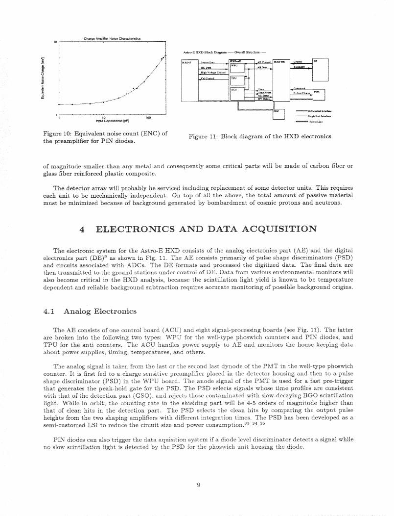
2.4 Low Noise Charge Amplifier
Improving tile energy resolution is the most demanding issue in developing our silicon PIN diode. The
energy resolution can be improved by optimizing the design of the preamplifier and the shaper amplifier, in
reality, however, the totM input capacitance (Ci_) which is the sum of the junction capacitances of two PIN
diodes (_ 2 x 20 pF) and the capacitance of the cables connecting the diodes to the preamplifiers (_ 30 pF)
will determine the resolution. 8 29 a0 We currently set our goal at an energy resolution of/XE(fwhra) '_ 3
keV at -20°C and are developing a low-power low-noise amp!ifier system optimized to this large input
capacitance. The current design gives the equivalent noise figure shown in Fig. 10.
3 HOUSING OF THE DETECTOR ARRAY
The mechanical vibration and shock is expected to be much higher for the M--V rocket of ISAS than for
rackets powered by liquid fuel and the housing for the detector array requires great care. The dissipation
of the heat generated by the AE parts placed in the housing (_ 15 W) poses additional constraint to the
design. Since the BGO crystal is quite brittle,some support mechanism must be installed to damp external
vibrations and to minimize the internal stress of BGO. The thermal expansion coefficientof BGO is an order
Charge Amplifier Noise Characteristics
Figure 10: Equivalent noise count (ENC) of
the preamplifier for PIN diodes.Figure 11" Block diagram of the HXD electronics
of magnitude smaller than any metal and consequently some critical parts will be made of carbon fiber or
glass fiber reinforced plastic composite.
The detector array will probably be serviced including replacement of some detector units. This requires
each unit to be mechanically independent. On top of all the above, the total amount of passive material
must be minimized because of background generated by bombardment of cosmic protons and neutrons.
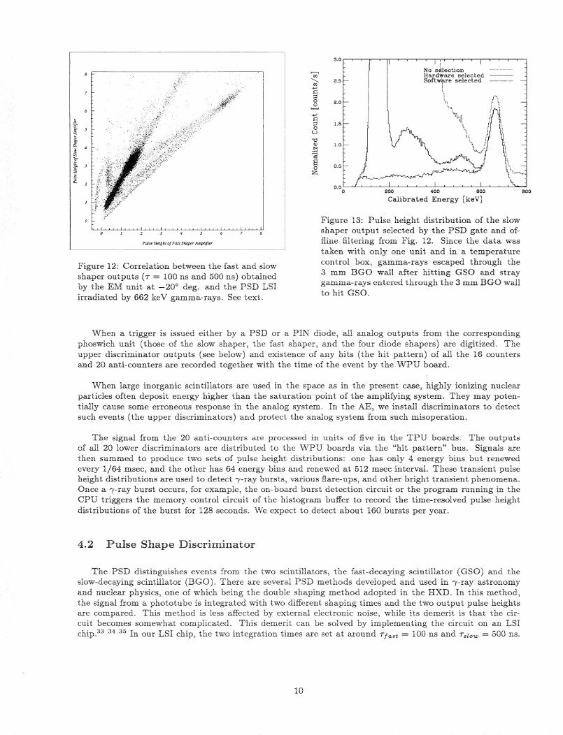
4 ELECTRONICS AND DATA ACQUISITION
The electronic system for the Astro-E HXD consists of the analog electronics part (AE) and the digital
electronics part (DE) 9 as shown in Fig. 11. The AE consists primarily of pulse shape discriminators (PSD)
and circuits associated with ADCs. The DE formats and processed the digitized data. The final data are
then transmitted to the ground stations under control of DE. Data from various environmental monitors will
also become critical in the HXD analysis, because the scintillation light yield is known to be temperature
dependent and reliable background subtraction requires accurate monitoring of possible background origins.
4.1 Analog Electronics
The AE consists of one control board (ACU) and eight signal-processing boards (see Fig. 1!)o The latter
are broken into the following two types: "WPU for the we!I-type phoswich counters and PIN diodes, and
TPU for the anti counters. The ACU handles power supply to AE and monitors the house keeping data
about power supplies, timing, temperatures, and others.
The analog signal is taken from the !ast or the second lastdynode of the PMT in the wei!-type phoswich
counter. It is firstfed to a charge sensitive preamplifier placed in the detector housing and then to a pulse
shape discriminator (PSD) in the WPU board. The anode signal of the PMT is used for a fast pre-trigger
that generates the peak-hold gate !%r the PSD. The PSD selects signals whose time profiles are consistent
with that of the detectioi_ part (GSO), and rejects those contaminated with slow-decaying BGO scintillation
light. While in orbit, the counting rate in the shielding part will be 4-5 orders of magnitude higher than
that of clean hits in the detection part. The PSD selects the clean hits by comparing the output pulse
heights from the two shaping amplifiers with different integration times. The PSD has been developed as a
semi-customed LSI to reduce the circuit size and power consumption, aa 34 as
PIN diodes can also trigger the data aquisition system if a diode level discriminator detects a signal while
no slow scinti!Iation light is detected by the PSD for the phoswich unit housing the diode.
Pulse Height of Fast Shaper Amplifier
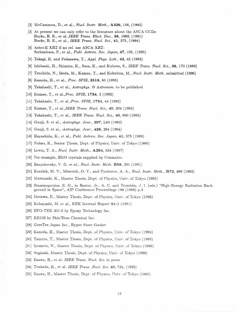
Figure 12: Correlation between the fast and siowshaper outputs (_- = 100 ns and 500 ns) obtainedby the EM unit at --20° deg. and the PSD LSIirradiated by 662 keV gamma-rays. See text°
r--n
[#1
OO
O
L)
CDt'q
O
z
3.0
1.5
1.0
0.5
0.0
0
i ........ li.... i ....No s_lection
:_- Hardware selected
i_ SoftwNre selected
.%
_i. ['! _
!
2oo 4oo 600 aoo
Calibrated Energy [keV]
Figure 13: Pulse height distribution of the slowshaper output selected by the PSD gate and of-fline filtering from Fig. 12. Since the data was
taken with only one unit and in a temperaturecontrol box, gamma-rays escaped through the3 mm BGO wall after hitting GSO and straygamma-rays entered through the 3 mm BGO waltto hit GSOo
When a trigger is issued either by a PSD or a PIN diode, all analog outputs from the correspondingphoswich unit (those of the slow shaper, the fast shaper, and the four diode shapers) are digitized. The
upper discriminator outputs (see below) and existence of any hits (the hit pattern) of all the 16 countersand 20 anti-counters are recorded together with the time of the event by the WPU board.
When large inorganic scintillators are used in the space as in the present case, highly ionizing nuclearparticles often deposit energy higher than the saturation point of the amplifying system. They may poten-
tially cause some erroneous response in the analog system. In the AE, we install discriminators to detectsuch events (the upper discriminators) and protect the anadog system from such misoperation.
The signal from the 20 anti-counters are processed in units of five in the TPU boards. The outputs
of all 20 lower discriminators are distributed to the WPU boards via the "hit pattern" bus. Signals are
then summed to produce two sets of pulse height distributions: one has only 4 energy bins but renewedevery 1/64 msec, and the other has 64 energy bins and renewed at 512 msec interval. These transient pulseheight distributions are used to detect _/-ray bursts, various flare-ups, and other bright transient phenomena.Once a "y-ray burst occurs, for example, the on-board burst detection circuit or the program running in theCPU triggers the memory control circuit of the histogram buffer to record the time-resolved pulse height
distributions of the burst for 128 seconds. We expect to detect about i60 bursts per year.
4.2 Pulse Shape Discriminator
The PSD distinguishes events from the two scintillators, the fast-decaying scintillator (GSO)and the
siow-decaying scintillator (BGO). There are severaI PSD methods developed and used in _/-ray astronomy
and nuclear physics, one of which being the double shaping method adopted in the HXD. In this method,the signal from a phototube is integrated with two different shaping times and the two output pulse heightsare compared. This method is less affected by external electronic noise, while its demerit is that the cir-cuit becomes somewhat complicated. This demerit can be solved by implementing the circuit on an LSI
chip 3a 34 as In our LSI chip, the two integration times are set at around Tf_ = 100 ns and %Zo_ = 500 ns.
10

The outputs of the two shapers have different pulse heights for BGO signals, while they are almost equal
for pure GSO signals. The pulse-shape discimination LSI has been developed using a semi-customed LSI
technology.aa a4 as Shown in Figs. 12 and 13 is the result of a test done by using the LSI circuit with the
phoswich unit of the Engineering Model: the irradiated gamma-rays are from 137Cs (662 keV). In Fig. 12,
the linear duster extending at an angle around 30 deg. to the ordinate, is due to hits on the BGO shielding
part while the one extending to right is due to clean hits on the GSO detection part. Compton scattered
gamma-rays form two linear dusters bridging between the blob corresponding to the clean hits on GSO and
either one of the two blobs corresponding to the bottom BGO and the coltimator BGO. One can see that
pure GSO events can be seperated from BGO events and Compton scatterd events. Fig. 13 shows how the
background is reduced by selection of the GSO cluster in Fig. 12 by the PSD chip and subsequent off-line
analysis. Since we have put only one unit in a temperature- controlled box, Compton-scattered gamma-rays
escaped or entered through the 3 mm BGO wall as apparent in Fig. 13. In the reaI detector, these v-rays
will be captured by neighboring units and rejected when the hit pattern is interrogated.
4.3 Digital Electronics
The DE controls acquisition of the data, coordinates among them, detects and reacts on requests for
services, and provides the primary interface with the satelIite data processor for command and telemetry
(see Fig. 11). These tasks are executed by a system consisting of one Intel S0386 running at 8 MHz. To
obtain a high data-acquisition rate, each AE board is capable of sending data by the DMA transfer mode
to the DE. Here the data for 64 events are blocked so that the interrupt rate to CPU remains low. 9
The CPU also performs some software event selections by examining the hit pattern around the unit in
which the trigger is initiated: this further reduces Compton scattered events and particie interaction events.
The CPU acquire cMibration data and data used to estimate background.
5 CALIBRATION AND MONITORING
On board calibration wilt be needed in the energy measurement by the PIN diodes and phoswich detectors.
For the diodes, we are examining possiblity of using t( X-rays from the phosphorus btonze of the fine
collimator. For GSO, the c_-rays emitted by a natural isotope lS2Gd, appearing at around E_ _ 385 keV
with a counting rate around _ 10-4/s/cm2/keV, will be used. 1° 11 i2 la 14
Critical items to be monitored include various counting rates that will be needed in estimating the
activation background. The temperature of the scintillators and phototubes are also to be monitored because
of their temperature dependence shown in Fig. 5.
6 EXPECTED BACKGROUNDS
Possible in-orbit backgrounds have been estimated for the present counter design: GSO of 2.4 x 2.4 x 0.5
cm a shielded by BGO of _ 5 cm thickness all around. 22 s The proton flux has been assumed to be that of the
model given in the reference 2a at the solar minimum., although the scheduled flight time corresponds roughly
to the solar maximum when the background is expected to be about half. 23 The results are summarized in
Tabie 2: one can see that the internal and cosmic-ray induced radioactivities wit1 be the dominant source
of background beiow 300 keV. We therefore anticipate that the sensitivity of HXD will be limited by these
induced radioactivities.
Among the listed background origins, prompt backgrounds produced by charged particles on BGO can
easily be rejected. Gamma-rays generated in passive material around the detector array have some chance
to leak through a few centimeter of BGO, if their energy is above _ 300 keV. We have to minimize passive
material close to the HXD detectors, eg. the HXD housing and the fine collimator. Gamma-rays generated
11

Table2: Expectedbackgroundrates
In-orbitactivationLeak-thru-/-rays
Off-aperture CXB
Radioactive impurities
: _ (0.5 .-_ 1) x 10 -s /sec/cm2/keV at 100 keV
: _ I x 10 .6 /sec/cm2/keV at 300 keV
2 x I0 -s /sec/cm2/keV at 400 keV
2 x 10 .4 /sec/cm2/keV at 500 keV
: _ 7 x 10 .6 /sec/cm2/keV at 50 keV
I x 10 .6 /sec/cm2/keV at 100 keV
: 5 _ I x 10 .6 /sec/cm2/keV below 300 keV
by nuclear interactions in the tip of the XRT complex have some chance to enter the FOV determined by
the BGO well.
What may become a dominant background and yet is difficult to estimate is faking of clean-hit GSO
events by pile-up of BGO hits or by Cherenkov photons in the P MT face windows. Background due to
radioactivity and amount of radioactivity that may be produced have been and still are actively studied by
bombarding the materials around the HXD detector with protons and by running the simulation programs. 22
Through these efforts and adequate on board monitoring, we expect to be able to predict the background
for actual observations to an accuracy better than _ 5%. We note that such predictions worked to about
1% 1eve1 in the Ginga-LAC. 16
7 CONCLUSIONS
The design and expected performance of the Hard X-ray Detector (HXD), one of the 3 experiments
aboard Astro-E have been presented. Most of its critical elements have been prototyped, tested, and verified
their validity. One item that still requires continuing R/D works is the 2 mm thick silicon PIN diodes. The
total weight and the total power consumption are to be reduced further. We expect the above issues to be
solved within this calendar year.
8 ACKNOWLEDGEMENTS
We wish to thank Dr. 1.1. Ishibashi of Hitachi Chemicai Co. Ltd. for collaboration in improving the
quality of GSO, Mr. T. Itoh of Bikowski Japan Coo Ltd. for assembty of the BGO wells, Messers I<. Taguchi,
M. Horii, M° Hamaya, S° Shinoda, and R. Shoumura of Meisei Electronics for detector and eiectronics
assembly, Messers To Hanazawa, t<. Shimizu, and Y. Sano of Fujitsu VLSI Ltd. for the anaIog LSI design
and production, Messers S. IKubo, Kiminori Sato, 1<eiji Sato, I. Odagi, and Y. Tanaka of Fujitsu Ltd. for the
DE part of electronics, and Dr. T. Sumiyoshi of KEK for measuring the reflectivity of the reflector sheets.
We acknowledge contributions by Ms. N. Yamasaki, Messers N. Tsuchida, T. Ohtsuka, and 14. Nagata to
the earlier phase of the R/D works on Astro-E HXD.
The present work was supported by Grant-in-Aid for Scientific Research No. 05242101 and Grant-in-Aid
for COE Research No. 07CE2002 by the Ministry of Education, Culture, and Science, Japan.
REFERENCES
[1] Inoue, H., Proc. of the 11th Colloquium on UV and X-Ray Spectroscopy of Astrophysical and Laboratory
Plasmas, Universal Academy Press (Tokyo, i995)
12
[4]
[5]
[6]
[7]
[8]
[9]
[io]
[11]
[12]
[14]
[151
[16]
[18]
[2o]
[2!I
[22]
[24]
[25]
[26]
[271
[zs]
[29]
[30]
[3zi
[32]
[33]
[a4]
[35]
McCammon, D., et al., Nucl. Instr. Meth., A326, 156, (1993)
At present we can only refer to the literature about the ASCA CCDs:
Burke, B. E., et al.,IEEE Trans. Elect. Dev., 38, 1069, (1991)
Burke, B. E., eta|., IEEE Trans. Nucl. Sci., 41,375, (1994)
Astro-E XRT if no ref. use ASCA XRT:
Serlemitsos, P., et al., PubL Astron. Soc. Japan, 47, 105, (1995)
Takagi, K. and Fukazawa, T., Appl. Phys. Lett., 42, 43 (1983)
Ishibashi, H., Shimizu, K., Susa, K., and Kubota, S., IEEE Trans. Nucl. Sci., 36, 170 (1989)
Tsuchida, N., Ikeda, M., Kamae, T., and Kokubun, M., Nucl. Instr. Meth. submitted (1996)
Kaneda, H., et aI., Proc. SPIE, 2518, 85 (1995)
Takahashi, T., et al., Astrophys. _ Astronom. to be published
Kamae, T., et al.,Proc. SPIE, 1734, 2 (1992)
Takahashi, T., et al.,Proc. SPIE, 1734, 44 (1992)
Kamae, T., et aI.,IEEE Trans. NucI. Sci., 40, 204 (1993)
Takahashi, T., et al., IEEE Trans. Nucl. Sci., 40, 890 (1993)
Gunji, S. et al., Astrophys. Jour., 397, L83 (1992)
Gunji, S. et at., Astrophys. Jour., 428, 284 (i994)
Hayashida, K., et al., PubL Astron. Soc. Japan, 41, 373 (1989)
Nakao, K., Senior Thesis, Dept. of Physics, Univ. of Tokyo (i990)
Lewis, T. A., NucL Instr. Meth., A264, 534 (1987)
For example, BGO crystals supplied by Crismatec.
Baryshevsky, V. G. et al., NucL Instr. Meth. B58, 291 (1991)
Korzhik, M. V., Miesvich, O. Vo, and Fyodorov, A. A., NucL Instr. Meth., B72,499 (1992)
IViatsuzaki, K., Master Thesis, Dept. of Physics, Univ. of Tokyo (1995)
Stassinopouios, E. G., in Rester, Jr., A. C. and Trombka, J. I. (eds.) "High-Energy Radiation Back-
ground in Space", AIP Conference Proceedings I86 (1989) p.3
Idesawa, E., Master Thesis, Dept. of Physics, Univ. of Tokyo (i996)
Kobayashi, M. et ai., KEN: Internal Report 91-1 (1991)
EPO-TEK 301-2 by Epoxy Technology Inc.
KE103 by Shin'Etsu Chemical Inc.
GoreTex Japan Inc., Hyper Sheet Gasket
Kaneda, H., Master Thesis, Dept. of Physics, Univ. of Tokyo (!994)
Tamura, T., Master Thesis, Dept. of Physics, Univ. of Tokyo (1995)
Iyomoto, N., Master Thesis, Dept. of Physics, Univ. of Tokyo (t996)
Sugizaki, Master Thesis, Dept. of Physics, Univ. of Tokyo (1996)
Ezawa, H., et al. IEEE Trans. Nucl. Sci. in press
Tsukada, K., et al. IEEE Trans. NucL Sci. 40, 724, (1993)
Ezawa, H., Master Thesis, Dept. of Physics, Univ. of Tokyo (1995)
13