Embed Size (px)
Citation preview

Fabrication process of Al small Josephson junctions for quantum bits
Mutsuo Hidaka and *Masaaki Maezawa
International Superconductivity Technology Center *National Institute of Advanced Industrial Science and Technology
December 14, 2011 General meeting of FIRST Quantum Information Processing Project
Collaborators ISTEC: T. Satoh, S. Nagasawa, K. Hinode and Y. Kitagawa AIST: R. Noguchi, M. Yamagishi, T. Horikawa and H. Akinaga
NTT: T. Maruyama

Rough image of integrated Al Q-bit
Cross section structure of JJ (Josephson junction)
Al (Base electrode & Lower wiring)
AlOx (Tunnel barrier) Al (Counter electrode)
Al (Upper wiring)
SiO2
Au/Ti pad
Pd resister
Al co-planer signal line ( Upper-wiring layer)
Q-bit 1~100/chip
~1 µm
~100 nm
JJ 50 nm □~100 nm□
Readout SQUID
Control line
Nb (Resonator) Wafer size: 4 inch
EBL region
First step: fabrication of Al small (∼50 nm) Josephson junctions

Challenges
• Deposition of smooth and grain size controlled Al.
• Patterning of small JJs( ∼50 nm).
• Etching Al small JJs by Chlorine RIE.
• Contact formation between JJs and the counter electrode.
• Etc.
Contact Formation by using CMP = Exposure of Counter Electrode of JJ
BAS JJ
SiO2 AlOx
CMP Polishing
Conventional Contact through Via-hole
BAS JJ
SiO2 AlOx

JJ thermal-SiO2
Si
Contact Formation Process sequence trilayer deposition (dc magnetron sputtering) etching SiO2 deposition (bias sputtering) CMP COU deposition (dc magnetron sputtering) etching
JJ thermal-SiO2
Si
JJ thermal-SiO2
Si
SiO2
JJ thermal-SiO2
Si
SiO2
SiO2

01/late CAD data + Al/AlOx/Al films sent to SCR JJ: EB lithography + etching + cleaning 02/25 wafers sent to ISTEC 02/28-03/03 BAS: EB lithography + dev. 03/07 BAS etching + cleaning 03/07 SiO2 deposition 03/08 CMP 03/08 COU: Al deposition 03/09 alignment window: EB lithography + dev. + etching 03/11 cleaning 03/30 wafer sent to Maruyama-san NTT May COU: EB lithography + dev. + etching + cleaning dicing Characterization: I-V, SEM, (TEM)
Al JJ Process Ver. 1
Earthquake

Damage by the earthquake • Unplanned stop of machines • Mechanical damage to buildings/machines - some need repairing • Limited electricity supply - no air-conditioning in cleanrooms • Leakage in waste-water pipelines in Tsukuba Central area

Al JJ Process Ver. 1 CAD Pattern
5 mm 2.
5 m
m
JJ-1 chip JJ size (from left to right) 0.1 μm x 2 0.3 μm x 2 0.6 μm x 2 1.0 μm x 2 3.0 μm x2 0.2 μm x1 0.4 μm x1 0.8 μm x1 2.0 μm x1
JJ-2 chip JJ size (μm) 0.8 0.3 0.8 0.3 0.8 0.3 0.8 0.3 JJ distance (μm) 2.0 2.0 1.5 1.5 1.0 1.0 0.5 0.5 COU gap (μm) 1.0 1.0 1.0 1.0 0.8 0.8 0.3 0.3
JJ-1 JJ-2
JJ-1 JJ-2 BAS
BAS hole for End-point-Detection

Endpoint Detection Trouble Pattern Size Dependence of CMP
Si
BAS
thermal-SiO2
SiO2
Si
Al
thermal-SiO2
SiO2
Measurement Measurement
Pattern in Process Ver. 1
BAS Pattern: too large Endpoint Detection Trouble
Under-polished or Over-polished CMP
height difference due to pattern-size-dependence of CMP

Si
Al
Thermal-SiO2
SiO2 Al
Al-JJ Cross-sectional SEM (SCR: Yamagishi)
Al Residue: insufficient ion milling ? EB resist development trouble ?
Al SiO2 Al Thermal-SiO2
Si SiO2: too thin CMP: over-polished ?
Optical Micrograph (NTT)

Optical Micrograph after Dicing Characterization (NTT)
JJ-BG 室温測定値 JJ径 A1 C1 C2 C3 E1 E2 E3
※測定系の抵抗値:4Ω程度 1 2.0 3.89 8.18 7.73 5.88 25.19 9.12 3.91
2 0.8 3.88 8.57 8.56 6.16 16.64 4.26 3.913 0.4 3.89 8.53 9.04 6.56 25.58 6.35 3.914 0.2 4.29 10.17 8.73 5.37 26.60 4.05 3.915 3.0 3.91 9.91 6.83 6.16 30.12 3.77 3.916 3.0 4.22 9.06 8.52 6.80 16.00 17.64 4.187 1.0 4.20 6.88 7.16 6.41 30.12 5.86 3.918 1.0 5.19 9.77 6.35 6.22 20.62 4.31 3.929 0.6 5.15 5.07 6.09 5.85 28.49 4.03 7.65
10 0.6 5.07 9.94 6.23 6.72 29.76 3.91 13.0711 0.3 5.00 10.73 7.13 5.99 39.68 5.09 3.9212 0.3 4.98 10.60 6.83 5.28 16.67 3.91 3.9213 0.1 6.10 10.78 7.08 7.14 41.67 9.47 3.9214 0.1 5.93 9.91 7.31 6.47 36.10 3.91 7.24
14 13 12 11 10 9 8 7 6 5 4 3 2 1
BG
2-probe Measurement at R.T.
4-probe Measurement at T = 14 mK E1 chip
40
20
0
-20
-40
Cur
rent
(µA
)
5000-500Voltage (µV)
E1-11
jj=0.3umφ
40
20
0
-20
-40
Curre
nt (µ
A)
400020000-2000-4000Voltage (µV)
E1-12
jj=0.3umφ
-40
-20
0
20
40
Curre
nt (µ
A)
2001000-100-200Voltage (µV)
E1-13
jj=0.1umφ
40
20
0
-20
-40
Curre
nt (µ
A)
400020000-2000-4000Voltage (µV)
E1-14
jj=0.1umφ

Next Process Ver. 2
Process Sequence No.1 No.2 1) Trilayer Deposition (ISTEC) 2) JJ Etching (SCR) 3) JJ Protection (JP) Layer 4) BAS Etching (SCR) 5) SiO2 Deposition (SCR or ISTEC) 6) CMP (ISTEC) 7) BC contact Etching (NPF/ISTEC) 8) COU deposition (ISTEC) 9) COU Etching (NPF/ISTEC) 3) JJ Protection Layer : PCVD SiO2 or Anordization 5) SiO2 Deposition : PCVD SiO2 or Bias-sputter SiO2
thermal-SiO2 Si
SiO2 JJ Al BAS
COU BC
We need ・Design: Small BAS Pattern to ensure end-point detection of CMP
・Ion Milling Optimization ・Readjustment of fabrication machines
JP

AIST facilities: status quo • Clean rooms restarted at
the end of July
• No long-term electricity cut-off
• No more electricity-saving requirement
• Restoration of most facilities and machines
• Condition changes for some machines re-adjustment
6
Roadmap towards Restoration’11/05 ’11/08 ’11/11 ’12/02
Bldg.2-8
machinerepair
Bldg. 4-4&2-2
machinerepair
normaloperation
normaloperation
normaloperation
NPF machinerepair
normaloperation
moving to somewhere
electricitycut off
electricitycut off?
normaloperation
SCR machinerepair
normaloperation
electricitycut off?
normaloperation
additionalwaste drain
waste p-line repair

Al/AlOx/Al JJ process ver. 2 layer material thickness method
I0 SiO2 300 nm therm-oxid.
M1 Al 200 nm sputtering
BR AlOx ~1 nm therm-oxid.
M2 Al 100 nm sputtering
I1 (a) SiO2 (b) AlOx
50 nm 10 nm
PECVD anodization
I2 SiO2 500 nm (a)PECVD (b)sputtering
M3 Al 150 nm sputtering • Feedback from ver. 1 bottom-electrode design, wiring layer etch • Other improvements protection layer, PECVD SiO2, resist slimming • Parallel processing of 2 variants (ver. 2-a/2-b)
bottom-electrode Al (M1)
SiO2 (I0)
wiring Al (M3)
upper-electrode Al (M2)
insulation SiO2(I2)
tunnel-barrierAlOx (BR)
protection(I1)
Substrate Si

Ver. 2: improvements (1) • Narrow bottom electrode design uniform planarization
• Wiring layer (M3) etch: - optimum ion-milling condition - additional wet etch after ion-milling
Al resist
Ar+
Ver. 2: improvements (2) • Additional protection layer
• Plasma enhanced CVD (PECVD) SiO2 (Ver. 2-a) - better coverage, lower defect-density - low growth temperature < 250C (cf. ~350C for standard semiconductor process)
PECVD SiO2 (ver. 2-a) anodized AlOx (ver. 2-b)
wet cleaning corrosion

Ver. 2: improvements (3) • Resist slimming technique high-aspect pillar-shape resist tumbling during development/cleaning EB resist slimming by dry O2 ashing
Al
Al
AlOx
resist O2 plasma
resist
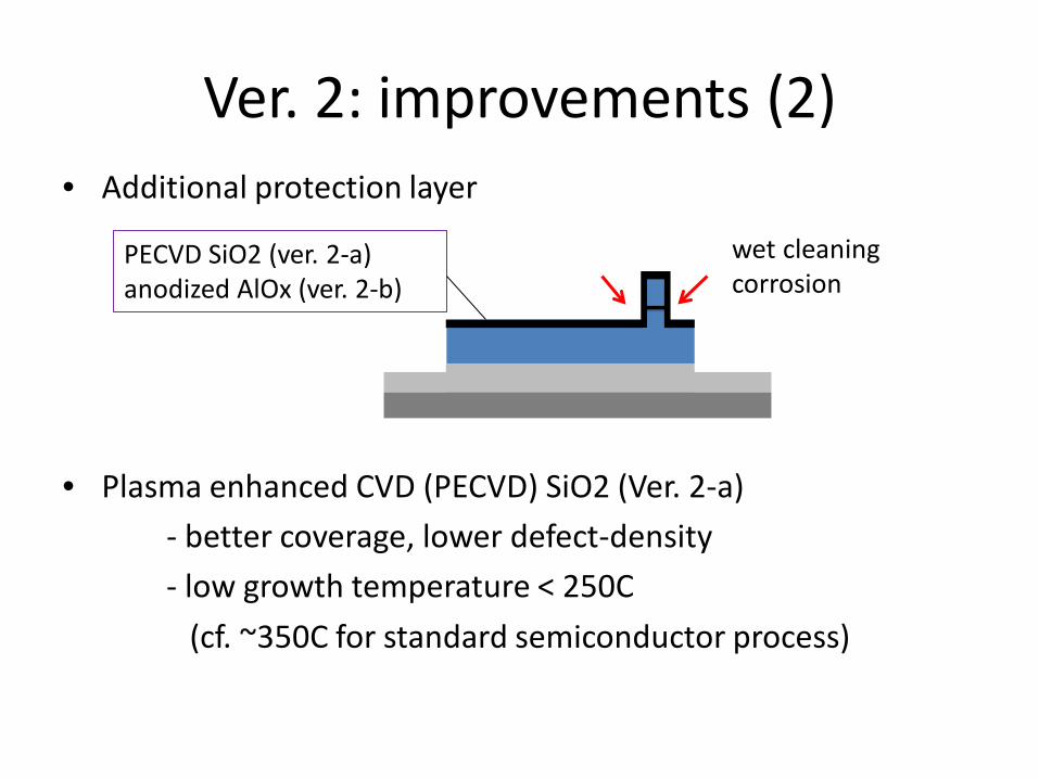
Ver. 2: process flow Ver. 2-a process facility
(1) Al/AlOx/Al deposition
SCR
(2) u-electrode patterning
(3) protection layer deposition PECVD SiO2
(4) b-electrode patterning
(5) insulation layer deposition PECVD SiO2
(6) planarization Bldg. 4-4
(7) via-hole patterning NPF Bldg. 2-8 (8) wiring deposition
(9) wiring patterning NPF Bldg. 4-4
Ver. 2-b process facility
(1) Al/AlOx/Al deposition SCR
(2) u-electrode patterning
(3) protection layer deposition anodized AlOx Bldg. 4-4
(4) b-electrode patterning NPF Bldg. 4-4
(5) insulation layer deposition sputtered SiO2 Bldg. 4-4 (6) planarization
(7) via-hole patterning NPF Bldg. 2-8 (8) wiring deposition
(9) wiring patterning NPF Bldg. 4-4
bottom-electrode Al (M1)
SiO2 (I0)
wiring Al (M3)
upper-electrode Al (M2)
insulation SiO2(I2)
tunnel-barrierAlOx (BR)
protection(I1)

Mask design

Preliminary result
Design 200nm 150nm 120nm 100nm
after EBL/dev
after slimming (ashing)
after RIE
189nm 132nm 91nm 56nm
171nm 114nm 71nm 41nm
168nm 109nm 64nm 33nm
Al patterning with resist slimming
0
50
100
150
200
250
0 50 100 150 200 250
actu
al s
ize
(nm
)
designed size (nm)
EB/DevSlimmingRIE
Successful fabrication of Al pillar with d < 50 nm

Short-term plan 2011 2012 06 08 10 11 12 01 02 03 04 05 06
facility restoration
ver. 1: testing & analysis
process definition
test mask design
process ver. 2
PECVD SiO2 optimization
fabrication ver. 2-a
fabrication ver. 2-b
testing
1st test qbit
process def.
device design

Summary
• Integration technology for supercond. qbits
• Earthquake during process ver. 1
• Unsuccessful results of ver. 1
• Process improvements in ver. 2