Embed Size (px)
Citation preview

General rights Copyright and moral rights for the publications made accessible in the public portal are retained by the authors and/or other copyright owners and it is a condition of accessing publications that users recognise and abide by the legal requirements associated with these rights.
• Users may download and print one copy of any publication from the public portal for the purpose of private study or research. • You may not further distribute the material or use it for any profit-making activity or commercial gain • You may freely distribute the URL identifying the publication in the public portal
If you believe that this document breaches copyright please contact us providing details, and we will remove access to the work immediately and investigate your claim.
Downloaded from orbit.dtu.dk on: Jul 17, 2018
Fabrication of 3D Air-core MEMS Inductors for High Frequency Power ElectronicApplications
Lê Thanh, Hoà; Mizushima, Io; Nour, Yasser; Tang, Peter Torben; Knott, Arnold; Ouyang, Ziwei; Jensen,Flemming; Han, AnpanPublished in:Microsystems & Nanoengineering
Link to article, DOI:10.1038/micronano.2017.82
Publication date:2018
Document VersionPublisher's PDF, also known as Version of record
Link back to DTU Orbit
Citation (APA):Lê Thanh, H., Mizushima, I., Nour, Y., Tang, P. T., Knott, A., Ouyang, Z., ... Han, A. (2018). Fabrication of 3DAir-core MEMS Inductors for High Frequency Power Electronic Applications. Microsystems & Nanoengineering,3, [17082]. DOI: 10.1038/micronano.2017.82

OPEN
ARTICLE
Fabrication of 3D air-core MEMS inductors for very-high-frequency power conversionsHoa Thanh Le1,2, Io Mizushima3, Yasser Nour2, Peter Torben Tang3, Arnold Knott2, Ziwei Ouyang2, Flemming Jensen1 and Anpan Han1
We report a fabrication technology for 3D air-core inductors for small footprint and very-high-frequency power conversions. Ourprocess is scalable and highly generic for fabricating inductors with a wide range of geometries and core shapes. We demonstratespiral, solenoid, and toroidal inductors, a toroidal transformer and inductor with advanced geometries that cannot be produced bywire winding technology. The inductors are embedded in a silicon substrate and consist of through-silicon vias and suspendedwindings. The inductors fabricated with 20 and 25 turns and 280-350 μm heights on 4-16 mm2 footprints have an inductance from34.2 to 44.6 nH and a quality factor from 10 to 13 at frequencies ranging from 30 to 72 MHz. The air-core inductors show threefoldlower parasitic capacitance and up to a 140% higher-quality factor and a 230% higher-operation frequency than silicon-coreinductors. A 33 MHz boost converter mounted with an air-core toroidal inductor achieves an efficiency of 68.2%, which is betterthan converters mounted with a Si-core inductor (64.1%). Our inductors show good thermal cycling stability, and they aremechanically stable after vibration and 2-m-drop tests.
Keywords: MEMS inductor; PwrSoC; TSVs; very high frequency; 3D
Microsystems & Nanoengineering (2017) 3, 17082; doi:10.1038/micronano.2017.82; Published online: 29 January 2018
INTRODUCTIONInductors and transformers are the fundamental building blocks ofelectronics, and they are found in every electronic device. Micro-inductors and transformers (now referred to as inductors) are usedin, for example, radio frequency microelectromechanical systems(RF MEMS)1–4, microactuators5,6, and biosensors7. Micro-inductorsfor power electronics is an emerging application in whichinductors are used as energy storage elements for switchedmode power supplies (SMPS). Miniaturization of SMPS has becomethe main focus for developing future generation power supplies,that is, power supply in package (PwrSiP) and power supply onchip (PwrSoC)8–10. The PwrSoC vision is to integrate all powerelectronics components on one chip. Higher integration lowersthe cost and increases both efficiency and power density.Therefore, one of the most important inductor requirements forPwrSoC technology is the CMOS compatibility for on-chipintegration. Other requirements are compact physical dimensions,a high-current capacity, and a high-quality factor for highefficiency10. Switching at very high frequencies (VHF, 30–300 MHz) is one route toward PwrSiP and PwrSoC11,12. In theVHF range, inductors with an air core or non-magnetic core arepreferred, as suitable magnetic materials working at thesefrequencies are limited and the core implementation is verychallenging13. For example, at 50 MHz, NiZn and CoNiZn have lowmagnetic saturation fluxes and cause detrimental core heating inhigh-flux power electronics applications14. In addition, VHFconverters require inductance values of 10 s of nH, which is inthe inductance range of air-core inductors, thereby lendingthemselves to a promising solution15.
The reported MEMS inductor fabrication technologies can beclassified into two main categories: on-substrate inductors andsubstrate-embedded inductors. To fabricate on-substrate planarinductors, surface micromachining technology has been widelyused, particularly for low-aspect-ratio inductors. These methodsare based on sacrificial layers16, molding17, or a combination ofthe two18. One method to fabricate on-substrate high-aspect-ratio3D inductors is to use UV-LIGA lithography with SU-8 negativeresist. The resist structures serve as electroplating molds andsacrificial layer19–21 or supporting pillars22,23 for the electrodeposi-tion of conducting metals. The second category is embeddedinductors, in which the inductors are embedded inside the Sisubstrate and utilize the unused substrate volume. Consequently,the inductor height above the substrate surface can be lowered,which is an advantage for integrated circuit implementation14.Si-embedded inductors are also an attractive solution for theadvanced packaging of ultra-compact power supplies with thepassive interposer24. There are prior-art studies of etched Sicavities for embedded inductors (wet-etched25 and dry-etched26)or through-silicon vias (TSV)24,26–28. Yu et al.26 reported aSi-embedded inductor using a fabrication process using 3Dshadow masks and multiple lithographical exposures with SU-8.The interconnections are not through wafer. By contrast, TSVinductors27 have the advantage of integrated circuit (IC) integra-tion, that is, co-packaged or stacked systems in a package29,30.MEMS TSVs are known to be a promising technology forminiaturized RF MEMS and advanced system packaging andintegration31,32. With the necessity of high-aspect-ratio TSVs forcompact 3D inductors, fabrication technology for Si-embeddedinductors is still a challenge.
1National Center for Micro- and Nanofabrication, Danchip, Technical University of Denmark, 2800 Kongens Lyngby, Denmark; 2Department of Electrical Engineering, TechnicalUniversity of Denmark, 2800 Kongens Lyngby, Denmark and 3IPU, Nils Koppels Allé, 2800 Kongens Lyngby, DenmarkCorrespondence: Anpan Han ([email protected])Received: 6 March 2017; revised: 22 August 2017; accepted: 14 September 2017
Microsystems & Nanoengineering (2017) 3, 17082; doi:10.1038/micronano.2017.82
www.nature.com/micronano

The near-ideal design of an air-core MEMS inductor involvesfree-standing windings where the remaining silicon is far from thewindings because the silicon negatively affects the operationfrequency and energy conversion efficiency due to parasiticcapacitance (Cp) and eddy-current losses that ultimately causesundesired heating. The parasitic capacitances between the Cuwindings and the Si substrate deteriorates the quality factor anddecreases the operation frequency26,33. In addition, there is also aneddy-current loss in the Si core34.In this paper, we implement a fabrication process of
Si-embedded 3D air-core inductors for VHF power conversionapplications. The inductors are embedded in the silicon substrate,and the suspended Cu windings are secured by Si fixtures(Figure 1). Our process has three main advantages. First, theprocess is CMOS-compatible with a maximum processingtemperature lower than 200 °C. This allows MEMS processing ofCMOS electronics wafers without harming the CMOS electronics.Second, the process is highly generic and enables the fabricationof a large diversity of inductor geometries. We demonstrate thediversity by fabricating spiral, solenoid, toroid, transformer, andthe ‘DTU’ inductor, which cannot be fabricated using wire-windingtechnology. The toroid geometry is especially well matched forPwrSoC applications because the magnetic field is confined in the
windings to reduce EMI and minimize the cross-talk effects onother proximity electronic components35. Third, the TSV-basedinductor technology enables the fabrication of a passiveinterposer with embedded 3D inductors for PwrSiP.The paper is presented as follows: The materials and fabrication
method are described with a process overview emphasizing thecritical steps. Then, the fabrication and characterization results arepresented. The inductors were tested with a small-signalmeasurement, reliability tests with thermal and mechanicalshocks, and large-signal testing in VHF converters. The last sectionconcludes the paper.
MATERIALS AND METHODSFabrication process overviewThe fabrication process includes three main stages, 12 steps and 4UV lithography masks (Figure 2). A 3D animation of the process isin Supplementary Video S1. We used 100-mm diameter, double-side polished, [100] crystal orientation, Si wafers. Stage 1 focuseson deep reactive ion etching (DRIE) TSV etching and begins withdepositing 50-nm-thick aluminum oxide (Al2O3) on both wafersides by atomic layer deposition (ALD). On the wafer front side, anAl2O3 hard mask is patterned by buffered hydrofluoric acid (BHF)
Toroidal windingsSolenoid windings
A′a b
ASi supportSi support
I in
I in
GGS
SGG
Iout
Iout
Figure 1 3D illustrations of the air-core toroidal inductor (a), and solenoid inductor (b). The input current (Iin) and output current (Iout) areindicated by the arrows. Ground-signal-ground (GSG) pads were designed for RF measurements. For the fabrication process of the crosssection A′-A, see Figure 2.
Stage 1: creating vias Stage 2: copper filling Stage 3: Si-core etching
1 6 11
12
13
14
15
7
8
9
10
2
2
4
5
Deposition of Al2O3 (Flat) Deposition of Al2O3 (deep-trench)Deposition Al2O3 and SiO2
Electroplating (top conductor)
Bottom-up electroplating
Electroplating (bottom conductor)
Copper wet etching
Photoresist (PR) Seed layers (Ti/Au)
Electroplated copper (Cu)Silicon dioxide (SiO2)
PR spin-coating + patterning PR spray-coating + patterning
Al2O3 and SiO2 etching (BHF)
Si-core etching (DRIE)
Inductor releasing (BHF)
Si fixture
Al2O3 etching (BHF)
Al2O3 removal (BHF)
Silicon (Si)
Aluminum oxide (Al2O3)
Through-silicon etching(DRIE) + PR stripping
3 μm 7 μm
Figure 2 Cross-sectional illustration of the fabrication process flow (section A-A′ in Figure 1a). BHF, buffered hydrofluoric acid; DRIE, deepreactive ion etching.
3D air-core inductors for VHF power conversionHT Le et al
2
Microsystems & Nanoengineering doi:10.1038/micronano.2017.82

etch using a photoresist mask (AZ MiR 701). Next, TSVs are createdby DRIE. The aspect ratio is from 9 to 12. The core shape is alsodefined in this step by the fixture trenches, which are between3 μm and 7 μm wide. Finally, the remaining resist and Al2O3 areremoved with an oxygen plasma and BHF. Stage 1 is finalized byan RCA cleaning step, which is an important preparation forstage 2.Stage 2 focuses on creating Cu TSVs and windings. First, Al2O3 is
deposited because it is crucial to cover and protect the deepfixture trenches (AR430) during the Si core removal (stage 3).Because of the high etching selectivity of Si over Al2O3 in an SF6plasma (100 000:1)36 only 50 nm of Al2O3 thin film is sufficient toprotect the Si support and fixtures (Figure 1b) while removing theSi core. Step 6 also includes the deposition of 1.5 μm SiO2 byplasma-enhanced chemical deposition. It partly seals the 3-μm-wide fixture trenches to avoid defects on the top windings.Subsequently, three electroplating steps are performed to form Cuwindings. We first plate a 30-μm-thick top layer and seal of theTSVs (step 7), followed by a bottom-up plating step to fill the TSVs(step 8); finally, a 30-μm-thick bottom layer (step 9) is plated. Forthe electroplating seed layer, we use an electron beam evaporated10 nm Cr and 100 nm Au thin-film stack. The inductor windingsare patterned by Cu wet etching using a resist mask, thusobtaining the Si-core inductor (step 10).In stage 3, the Si core is selectively removed by inductively
coupled plasma (ICP) etching. During the ICP etch, Cu is protectedby a 50-nm-thick Al2O3 layer from the plasma environment as anadditional precaution (step 11). A spray-coated photoresistuniformly covers the 30-μm-tall Cu windings and, more impor-tantly, seals the fixture trench (step 12). The spray-coating recipewas carefully developed. Photolithography is then performed onthe wafer front side, followed by BHF etching of Al2O3 and SiO2 toexpose the silicon (step 13) for isotropic silicon ICP etching (step14). The Al2O3 layers on the fixture trenches and at the waferbackside act as an ICP etch stop, allowing complete removal of theSi core. The windings are anchored by several Si fixtures andsuspended on the Al2O3/SiO2 membrane. The final air-coreinductor is obtained by removing the oxides in BHF.
Critical processes and process parametersIn this section, we describe the critical equipment, materials, andprocess parameters optimized for our process flow. We focus onthe ALD of Al2O3 (steps 1, 6, and 11), DRIE for TSV etching (step 4),Cu electroplating for TSVs and inductor windings (steps 7–9),photoresist spray coating for BHF etching of Al2O3 and SiO2 (step12), and isotropic ICP etching of the Si core (step 14).For steps 1, 6, and 11, a thermal ALD instrument (Picosun R200,
Espoo, Finland) deposits Al2O3, which serves as both the DRIE etchmask and the stopping barrier. Here a 50-nm-thick Al2O3 film isALD-deposited at 200 °C using alternating exposures of trimethy-laluminium (TMA) (Strem Chemical, MA, USA) and H2O. The reactorpressure was below 2 kPa during deposition. We developed tworecipes for flat surface (step 1) and deep trenches (AR= 32) (steps6 and 11), respectively. For flat wafers, one ALD reaction cycleconsists of one pulse and purge step for each precursor. Togetherwith the carrier gas (N2), the precursor gasses are pulse injectedinto the reactor, and the reactor is subsequently purged with thecarrier gas. The pulse time is 0.1 s, and the purge time for TMA andH2O are 3 and 4 s, respectively. For deep trenches, the secondrecipe has two pulse and purge steps for each precursor. For bothprecursors, the first pulse is 0.1 s followed by 0.5 s of purging,whereas the second pulse is 0.1 s followed by 20 s of purging37.The carrier gas flow is 150 sccm and 200 sccm for the TMA andH2O precursor, respectively. The deposition rates of both recipesare 1 Å per cycle. The thin-film thickness is measured usingspectroscopic ellipsometry (M-2000V, HAWoollam, Inc., Lincoln,Nebraska, USA).
For step 4, a DRIE tool (Pegasus, SPTS, UK) etches TSVs and thefixture trenches. The etch mask stack includes 2-μm-thick MiR 701photoresist (Microchem, Inc., USA) and a 50-nm-thick Al2O3 layer.The Al2O3 layer on the wafer back side acts as a stopping layerwhen etching through the Si wafer. For etching silicon TSVs andfixtures, we developed a two-segment recipe including a fastetching segment (segment A) and a notching-compensationetching segment (segment B) for the final part of the TSV. For bothsegments, coil powers are 2800 W and 2000 W in the etch andpassivation steps, respectively. The process temperature is 20 °Cfor segment A and 10 °C for segment B. Segment A is used to etch95% of Si in the wafer thickness, whereas the remainder is etchedwith segment B. The plasma chamber is pre-conditioned by10 min of an oxygen plasma before DRIE of silicon. Segment A isoptimized for high-speed etching with an etch rate of11 μmmin−1 with a 5% etch load. This recipe is based on theBosch process with three alternating steps, including sidewallpassivation (4 s, 200 sccm C4F8, 25 mTorr), boost (1.5 s, 350 sccmSF6, 25 mTorr, platen power 140 W), and Si etch (5 s, 550 sccm SF6,150 mTorr). Segment B uses a low-frequency platen generator(380 KHz) to minimize notching38 at the Al2O3 stop layer. The twomain steps are Si etching (3 s, 400 sccm SF6 and 40 sccm O2) andpassivation (2 s, 250 sccm C4F8).For steps 7–9, electroplating is used to deposit Cu as the
conductor material. It is done in a custom-designed chemical bathand setup39. Briefly, the electroplating bath consists of twotitanium bars holding a Cu anode and a cathode, which isconnected to the sample. The electrolyte contains 140 g L−1
CuSO4, 140 g L−1 H2SO4, and 66 mg L−1 NaCl. Air bubbling is usedfor electrolyte agitation. Electroplating is performed at roomtemperature. Two processes are developed for, respectively,plating a 30-μm-thick Cu layer on a planar surface (steps 7 and9) and bottom-up filling into TSVs (step 8). Dedicated waferholders for each processes have been designed. One key featureof the holder for the first process is the stainless steel ‘currentthief’ for excellent plating-thickness uniformity across a 100-mmwafer (o5% peak to peak). The holder for the second process hasa stainless steel plate connected to a pin to achieve electriccontact from the bottom of the wafer and a plastic cover to fix thewafer and avoid plating at the edge. First, for the planar platingstep, it is important to seal the TSVs to provide an electrical pathfor TSV filling. A pulsed current with an average current density of2.57 A dm−2 is tested to be effective in closing the TSVs. Second,for TSV filling, a direct DC current at a density of 0.3 A dm−2 isused. A degassing step is required for both TSV closing and fillingto achieve void-free Cu-filled TSVs. For degassing, the Si wafer isimmersed in water and kept in vacuum (desiccator) for 10 minbefore abrupt venting. Trapped air bubbles expand in a vacuumand escape from cavities. This step is repeated several times untilno bubbles appear, after which the wafer is mounted on theplating holder. Despite degassing, the plating process is notuniform, and some TSVs would be filled and over-plated beforeothers. This problem is solved by removing over-plated Cu with a‘shaving’ process using a stainless-steel blade. Because silicondioxide and alumina are much harder than stainless steel, theshaving process does not scratch the sample mirror finish, which isrequired for subsequent processes. The filling process is thencontinued for the unfilled TSVs. This shaving-filling procedure isrepeated several times until all TSVs are uniformly filled. More than98% of TSVs are filled successfully with this process. Top andbottom Cu layers are then etched with a photoresist mask (AZ4562, Microchem, Inc.) using a commercial wet etchant (APS 100,Transene, MA, USA). The etch rate is ~ 0.5 μmmin−1 at roomtemperature.For step 12, a spray-coating instrument (ExactaCoat, Sono Tek
Co.) is used for uniform resist-layer coating of the 30-μm-tall Cuwindings and, more importantly, for sealing the fixture trenches.The spray-coated resist is then used (step 12) as a mask for etching
3D air-core inductors for VHF power conversionHT Le et al
3
Microsystems & Nanoengineeringdoi:10.1038/micronano.2017.82

Al2O3 and SiO2 using BHF (step 13). The photoresist, AZ4562, isdiluted in methyl ethyl ketone and propylene glycol monomethylether acetate with an optimized mixing ratio of 10:2:1. A two-stepspray coating recipe is developed to simultaneously cover the Cuwindings and seal the fixture trenches, which are 3 and 7 μmwide. The resist is sprayed twice with a 1-min waiting time at 28 °Cand the following parameters: The spray nozzle is 30 mm abovethe substrate, moving along a meandering path at a speed of10 mm s−1. The resist dispense rate is 2500 μl min−1. The distancebetween two spraying lines is 5 mm. The substrate temperatureis kept at 28 °C. To avoid air bubbles in the resist, the resistsolvents trapped in the trenches are slowly evaporated by storingthe samples for 5 h at room temperature. Then, the resist ispre-exposure baked in a convection oven at 90 °C for 30 min.The resist thickness on flat areas is 6 μm. Multiple exposures(4 exposures, 10 s waiting time between exposures, and a totaldosage of 420 mJ cm−2) are necessary to avoid resist overheating.The sample is then developed for 300 s using AZ 351B(Microchem, Inc.) diluted in deionized water with a volume ratioof 1:5. Hard-baking is done in a convection oven at 150 °C for30 min.For step 14, an ICP silicon-etching tool (STS MESC Multiplex ICP,
SPTS, Newport, UK) removes the silicon core and realizes the finalair-core inductors. We developed a fluorine-based isotropic ICPrecipe utilizing the undercut effect to etch Si in the toroidal core.The etch gasses are 230 sccm SF6 and 23 sccm O2. The coil poweris 2800 W, and a minimal platen power of 3 W is applied formaximal isotropic etching. The etch rate of the Si core is10 μmmin− 1. The spray-coated resist and a 50-nm-thick Al2O3
stack serve as the etch mask. The wafer backside is coated by 50-nm-thick Al2O3 and two layers of the spray-coated resist. TheAl2O3 layer stops the etching and prevents leaking of helium forbackside substrate cooling.
RESULTS AND DISCUSSIONFabrication resultsWe successfully fabricated 3D air-core inductors. Scanningelectron microscopy (SEM) micrographs show toroidal inductors,solenoids, spirals, and a 1:1 transformer (Figure 3). In addition, wecan also create inductors with arbitrary shapes; this is demon-strated by the ‘DTU’ inductor. The process achieved a yield of64–95% (Supplementary Figure S4).In this study, we fabricated 15 different toroidal inductor
designs with footprints from 4 mm2 to 16 mm2, an outer radius(Ro) from 0.5 mm to 2 mm, and an inner radius (Ri) from 0.5 to1 mm. The number of turns varies from 15 to 35 turns. Inductorswith 30-μm-diameter TSVs were realized on 280-μm-thick and350-μm-thick Si substrates. Thicker substrates can also be usedwith our process. We created inductors on a 500-μm-thicksubstrate with 50-μm TSVs. The inductors were designed withseveral TSVs in the outer ring to enhance volume coverage andminimize resistance. In addition, the identical diameter of TSVsachieves a uniform through-wafer etching and Cu TSV filling. Asdescribed before, the Si core has been removed to realize thedesired air-core and suspended windings structure. The releaseprocess includes BHF dipping, deionized water rinsing, and gentlenitrogen gas drying. After the release, we did not observe anydeformation of the windings. The inductors are suspended on theSi support and secured by symmetrically placed Si fixtures. Ourinductors are made of only Si and Cu; no polymers (for example,PDMS or SU-8) are used. We expect the inductors to have goodthermal stability, and low stresses are anticipated due to the lowerthermal expansion coefficient (CTE) mismatch between Cu andSi (ΔCTE Cu-Si = 14.1 ppm per °C), compared with Cu and SU-8(ΔCTE Cu-SU-8 = 35.3 ppm per °C). The inductor windings are freehanging and only secured in the Si fixtures. Only at the fixtures,there may be higher stress due to the direct Si-Cu contact. To
500 μm
a b
c
ed
500 μm
500 μm
500 μm
500 μm
500 μm
I in
Iout
GS
G
G
GS
Primary coil
Secondary coil
Figure 3 SEM micrographs of the fabricated 3D air-core MEMS inductors, (a) toroidal inductors with 16 mm2 (1.5 mm outer radius, 0.75 mminner radius, and 25 turns) and 4 mm2 footprint (inset). Presented by the lines and arrows, the current flows from the top wire bonding pad,through the TSV interconnects, then passes through the windings and exits at the lower pad. The measurement pads are designed in aground-signal-ground configuration at both terminals for wafer-level probing. Four 800 μm by 800 μm pads at the corners are for flip-chipbonding. (b) 1:1 toroidal transformer. The primary coil has larger conductors than that of the secondary coil. (c) Solenoid inductor, (d) spiralinductor, (e) ‘DTU’ inductor. SEM, scanning electron microscopy; MEMS, microelectromechanical systems; TSV, through-silicon vias.
3D air-core inductors for VHF power conversionHT Le et al
4
Microsystems & Nanoengineering doi:10.1038/micronano.2017.82
enable post processing of CMOS wafers, we kept all processtemperatures below 200 °C.In the following, the fabrication results of each step are
presented and discussed. Design considerations and technologychallenges are described.
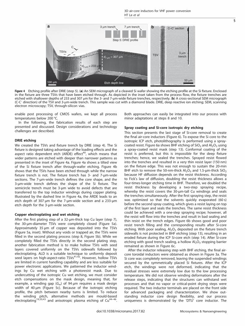
DRIE etchingWe created the TSVs and fixture trench by DRIE (step 4). The Sifixture is designed taking advantage of the loading effects and theaspect ratio dependent etch (ARDE) effect40, which means thatwider patterns are etched with deeper than narrower patterns aspresented in the inset of Figure 4a. Figure 4a shows a tilted viewof the Si fixture trench after through-wafer etching. Figure 4bshows that the TSVs have been etched through while the narrowfixture trench is not. The fixture trench has 3- and 7-μm-widesections. The 7-μm-wide trench defines the core shape, and the3-μm-wide trench defines the shape of the Si fixture. Thesemicircle trench must be 3-μm wide to avoid defects that aretransferred to the top inductor windings during copper plating.Illustrated by the dashed line in Figure 4a, the ARDE leads to anetch depth of 307 μm for the 7-μm-wide section and a 233-μmetch depth for the 3-μm-wide section.
Copper electroplating and wet etchingAfter the first plating step of a 32-μm-thick top Cu layer (step 7),the 30-μm-diameter TSVs were completely closed (Figure 5a).Approximately 35 μm of copper was deposited into the TSVs(Figure 5a, inset). Without any voids or trapped air, the TSVs werefilled in the second plating process (step 8, Figure 5b). While wecompletely filled the TSVs directly in the second plating step,another fabrication method is to make hollow TSVs with seedlayers covered uniformly on the TSVs sidewalls followed byelectroplating. ALD is a suitable technique to uniformly depositseed layers on high-aspect-ratio TSVs41,42. However, hollow TSVsare limited in current handling capability and are less suitable forpower electronic applications. We patterned the inductor wind-ings by Cu wet etching with a photoresist mask. Due toundercutting of the isotropic Cu wet etching, we must consideretch compensations on the mask design, meaning that, forexample, a winding gap (Gw) of 94 μm requires a mask designwidth of 40 μm (Figure 5c). Because of the isotropic etchingprofile, the pitch between nearby turns is limited. To reducethe winding pitch, alternative methods are mould-basedelectroplating19,20,43 and anisotropic plasma etching of Cu44–46.
Both approaches can easily be integrated into our process withminor adaptations at steps 8 and 10.
Spray coating and Si-core isotropic dry etchingThis section presents the last stage of Si-core removal to createthe final air-core inductors (Figure 6). To expose the Si core to theisotropic ICP etch, photolithography is performed using a spray-coated resist. Figure 6a shows BHF etching of SiO2 and Al2O3 usinga spray-coated resist mask (step 13). Conformal coating of theresist is preferred, but this is impossible for the deep fixturetrenches; hence, we sealed the trenches. Sprayed resist flowedinto the trenches and resulted in a very thin resist layer (150 nm)on the fixture edge. This was not enough to sustain the 20-minBHF etch to remove the 50-nm-thick Al2O3 and 1.5-μm-thick SiO2
because HF diffusion depends on the resist thickness. Accordingto Fick’s law of diffusion, doubling the resist thickness allows afour-times-longer etching time in BHF. Therefore, we doubled theresist thickness by developing a two-step spraying recipe,whereby the resist covers the 30-μm-tall Cu windings and sealsthe trenches simultaneously. After the first spraying step, the resistwas optimized so that the solvents quickly evaporated (60 s)before the second spray coating, which gives a resist laying on topof the first layer and seals the trenches. The same resist thicknesscould be achieved with a one-step spraying recipe; however, allthe resist will flow into the trenches and result in bad sealing andthin resist on the trench edges. Figure 6b shows good and poorresist trench filling and the corresponding results after Si-coreetching. With poor sealing, Al2O3 deposited on the fixture trenchsidewalls is not protected in BHF etching (step 13), resulting in aneroded fixture during the ICP Si-core etch (step 14). After Si-coreetching with good trench sealing, a hollow Al2O3 stopping barrierremained as shown in Figure 6c.After the inductor releasing step with BHF etching, the final air-
core toroidal inductors were obtained as shown in Figure 3a. TheSi core was completely removed, leaving the suspended windingssecured by the symmetrically placed Si fixtures. After the ICPetch, the windings were not deformed, indicating that theresidual stresses were extremely low due to the low processingtemperature. We did not observe winding deformations after therelease steps, indicating that the structures can withstand wetprocesses and that no vapor or critical-point drying steps wererequired. The two inductor terminals are placed on the front sidefor advanced packaging and characterization. We show out-standing inductor core design flexibility, and our processuniqueness is demonstrated by the ‘DTU’ core inductor. The
3 μm trench
3 μmtrench
C–C′ section
50 μm
7 μm trench
Step 5: DRIE profile
TSVTSVs
C
a b
C′
100 μm Etch depth line
d3 μm = 233 μm
d7 μm = 307 μm
Figure 4 Etching profile after DRIE (step 5). (a) An SEM micrograph of a cleaved Si wafer showing the etching profile at the Si fixture. Enclosedin the fixture are three TSVs that have been etched through. As depicted in the inset taken from the process flow, the fixture trenches areetched with shallower depths of 233 and 307 μm for the 3- and 7-μm-wide fixture trenches, respectively. (b) A cross-sectional SEM micrograph(C-C′ direction) of the TSV and 3-μm-wide trench. This sample was cut with a diamond blade. DRIE, deep reactive ion etching; SEM, scanningelectron microscopy; TSV, through-silicon vias.
3D air-core inductors for VHF power conversionHT Le et al
5
Microsystems & Nanoengineeringdoi:10.1038/micronano.2017.82

other approach to remove the Si core is potassium hydroxide(KOH) Si wet etching, but the core geometries are heavilyrestricted, that is, square rectangular cores are possible. TheKOH is, however, a cheaper batch process.
Small signal measurementOur MEMS inductors were electrically characterized in the frequencyrange from 1 to 110 MHz using a precision impedance analyzer(Agilent 4294A, Agilent Technologies Inc., Santa Clara, CA, USA). Themeasurements were done for four toroidal inductor designs: (i) 280-μm-tall and 25-turn air-core inductors, (ii) 280-μm-tall and 20-turnair-core inductors, (iii) 350-μm-tall and 20-turn air-core inductors,and (iv) 280-μm-tall and 20-turn Si-core inductors. The inductorshave a 0.75-mm inner radius, a 1.5-mm outer radius, and a TSV
diameter of 30 μm. For each design, we measured three inductors,and for Figure 7, 12 inductors in total were measured. More detailson the inductor design, modeling, and measurement will bepresented in our upcoming paper.Figure 7a shows the measurement results for three inductors of
design (i). The measured inductance and resistance values are20% larger than simplified analytical calculations of ideal toroidinductors. At the peak quality factor (Q) frequency (41.2 MHz),the inductance is 34.3 nH± 0.12 nH, and Q is 12.9 ± 0.17. Theresistance is 180 ± 7 mΩ at 1 MHz. The inductors were from thesame wafer. For all measurement points, the average peak-to-peakvariations are 0.56% (inductance), 2.67% (quality factor), and2.56% (resistance), respectively. We have also compared theinductors from two different process runs. Ten toroidal inductorswith 280 μm thick and 20 turns were measured. The standard
3 μm trencha b c
7 μm trench
TSVs
20 μm
100 μm 30 μm 100 μm
40 μm
Gw=94 μm
Figure 5 Cu electroplating and wet-etching results. (a) A top-view SEM micrograph after the first plating of the 30-μm-thick Cu layer (step 7).All TSVs and the fixture trench are closed, which provides the electrical path for bottom-up TSV filling. The transparent red line illustrates thefixture trenches that have been closed. Copper is filled 35 μm into the TSVs, as shown in the subfigure. (b) A void-free Cu-filled TSV after 13.5 hof plating at 0.5 A dm− 2 (step 8). (c) Wet-etched toroidal Cu windings (step 9). The red lines are isotropic wet-etch compensations on thephotolithography mask design. The winding pitch (Gw) is increased from the designed 40 to 94.3 μm due to the lateral undercut. SEM,scanning electron microscopy; TSV, through-silicon vias.
Spray resist
a b c
d
500 μm
SiGood filling Al2O3-coated
fixture trench
Al2O3
Bad filling
Eroded
B
B′
B–B′Resist
Si
Backside
87 μm
200 μm
200 μm
500 μm
149 μm
500 μm
Figure 6 (a) Optical top-view micrograph of the patterned spray-coated resist at the Si fixture (step 12). Good and bad fixture trench resistsealing are shown in the top and bottom insets. (b) Si-core etching results corresponding to good and bad sealing. (c) A hollow Al2O3stopping barrier on the fixture trench (cross section is depicted in the inset) and an Al2O3/SiO2 membrane at the bottom remained afterisotropic ICP Si etching. (d) A well-defined Si fixture was on the final inductor after the BHF releasing step, and the fixture backside is shown inthe inset. BHF, buffered hydrofluoric acid; ICP, inductively coupled plasma.
3D air-core inductors for VHF power conversionHT Le et al
6
Microsystems & Nanoengineering doi:10.1038/micronano.2017.82
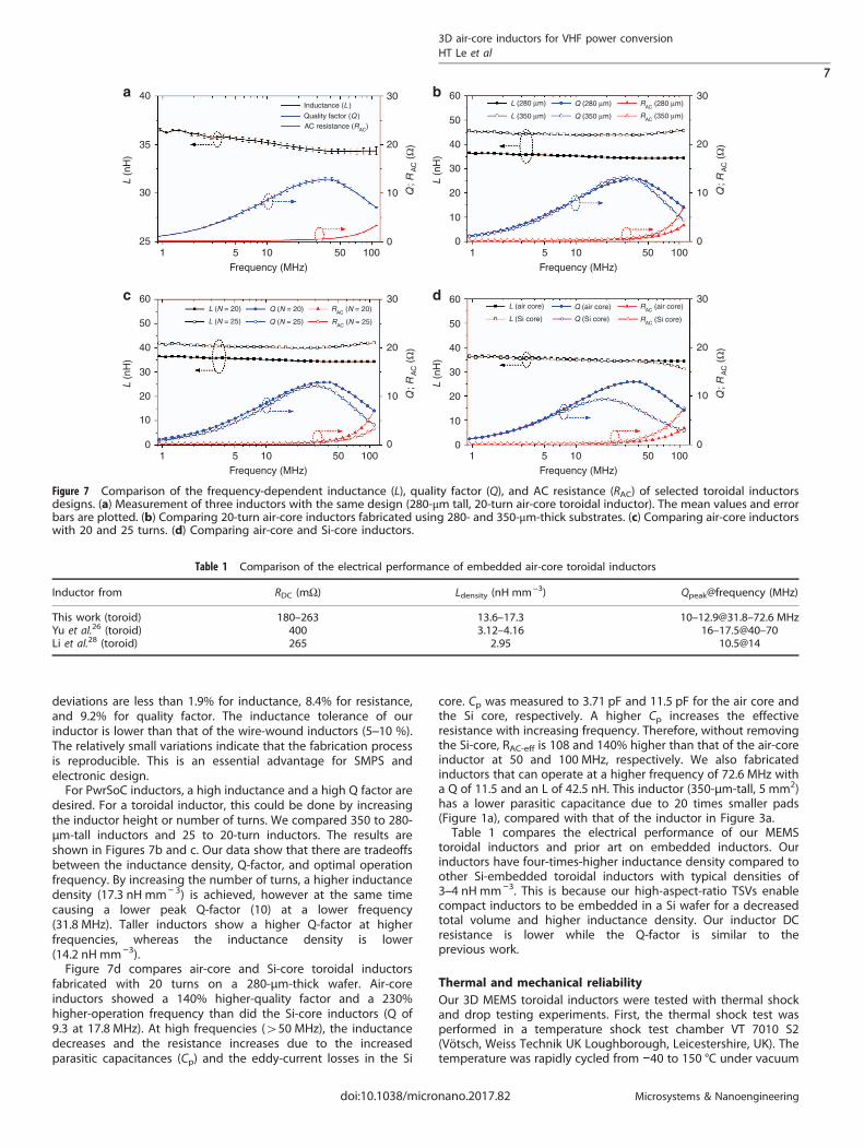
deviations are less than 1.9% for inductance, 8.4% for resistance,and 9.2% for quality factor. The inductance tolerance of ourinductor is lower than that of the wire-wound inductors (5–10 %).The relatively small variations indicate that the fabrication processis reproducible. This is an essential advantage for SMPS andelectronic design.For PwrSoC inductors, a high inductance and a high Q factor are
desired. For a toroidal inductor, this could be done by increasingthe inductor height or number of turns. We compared 350 to 280-μm-tall inductors and 25 to 20-turn inductors. The results areshown in Figures 7b and c. Our data show that there are tradeoffsbetween the inductance density, Q-factor, and optimal operationfrequency. By increasing the number of turns, a higher inductancedensity (17.3 nH mm− 3) is achieved, however at the same timecausing a lower peak Q-factor (10) at a lower frequency(31.8 MHz). Taller inductors show a higher Q-factor at higherfrequencies, whereas the inductance density is lower(14.2 nH mm−3).Figure 7d compares air-core and Si-core toroidal inductors
fabricated with 20 turns on a 280-μm-thick wafer. Air-coreinductors showed a 140% higher-quality factor and a 230%higher-operation frequency than did the Si-core inductors (Q of9.3 at 17.8 MHz). At high frequencies (450 MHz), the inductancedecreases and the resistance increases due to the increasedparasitic capacitances (Cp) and the eddy-current losses in the Si
core. Cp was measured to 3.71 pF and 11.5 pF for the air core andthe Si core, respectively. A higher Cp increases the effectiveresistance with increasing frequency. Therefore, without removingthe Si-core, RAC-eff is 108 and 140% higher than that of the air-coreinductor at 50 and 100 MHz, respectively. We also fabricatedinductors that can operate at a higher frequency of 72.6 MHz witha Q of 11.5 and an L of 42.5 nH. This inductor (350-μm-tall, 5 mm2)has a lower parasitic capacitance due to 20 times smaller pads(Figure 1a), compared with that of the inductor in Figure 3a.Table 1 compares the electrical performance of our MEMS
toroidal inductors and prior art on embedded inductors. Ourinductors have four-times-higher inductance density compared toother Si-embedded toroidal inductors with typical densities of3–4 nH mm−3. This is because our high-aspect-ratio TSVs enablecompact inductors to be embedded in a Si wafer for a decreasedtotal volume and higher inductance density. Our inductor DCresistance is lower while the Q-factor is similar to theprevious work.
Thermal and mechanical reliabilityOur 3D MEMS toroidal inductors were tested with thermal shockand drop testing experiments. First, the thermal shock test wasperformed in a temperature shock test chamber VT 7010 S2(Vötsch, Weiss Technik UK Loughborough, Leicestershire, UK). Thetemperature was rapidly cycled from −40 to 150 °C under vacuum
40a b
c d60
50
40
30
20
10
01 5 10 50 100
35
30
251 5 10
Frequency (MHz)
Frequency (MHz) Frequency (MHz)
L (n
H)
L (n
H)
50
Inductance (L )
Quality factor (Q )AC resistance (RAC)
100 1 5 10
L (280 μm)
L (air core) Q (air core)
Q (Si core)L (Si core)L (N = 20) Q (N = 20)
Q (N = 25)L (N = 25)
RAC (280 μm)
RAC (N = 20)
RAC (N = 25)
RAC (350 μm)
RAC (air core)
RAC (Si core)
Q (280 μm)
Q (350 μm)L (350 μm)
Frequency (MHz)
L (n
H)
L (n
H)
Q; R
AC (
Ω)
Q; R
AC (
Ω)
Q; R
AC (
Ω)
Q; R
AC (
Ω)
50 100
1 5 10 50 100
30 60 30
20
10
0
30
20
10
0
50
40
30
20
10
0
60
50
40
30
20
10
0
20
10
0
30
20
10
0
Figure 7 Comparison of the frequency-dependent inductance (L), quality factor (Q), and AC resistance (RAC) of selected toroidal inductorsdesigns. (a) Measurement of three inductors with the same design (280-μm tall, 20-turn air-core toroidal inductor). The mean values and errorbars are plotted. (b) Comparing 20-turn air-core inductors fabricated using 280- and 350-μm-thick substrates. (c) Comparing air-core inductorswith 20 and 25 turns. (d) Comparing air-core and Si-core inductors.
Table 1 Comparison of the electrical performance of embedded air-core toroidal inductors
Inductor from RDC (mΩ) Ldensity (nH mm−3) Qpeak@frequency (MHz)
This work (toroid) 180–263 13.6–17.3 10–[email protected]–72.6 MHzYu et al.26 (toroid) 400 3.12–4.16 16–17.5@40–70Li et al.28 (toroid) 265 2.95 10.5@14
3D air-core inductors for VHF power conversionHT Le et al
7
Microsystems & Nanoengineeringdoi:10.1038/micronano.2017.82

for 250 cycles. The heating rate was 3 °C min−1, and the coolingrate was 3.5 °C min−1. We tested eight inductors: four air-coreinductors (TSV diameters of 30 and 50 μm) and four Si-coreinductors (TSV diameters of 30 and 50 μm). After 250 cycles, theinductors were optically inspected and electrically characterized.All inductors were electrically functional, and no deformation orcracks were observed. More details of the testing results can befound in Supplementary Figures S1 and S2.Second, drop testing experiments were conducted to probe the
mechanical stability of the suspended windings. The inductorswere mounted on a PCB test board, which then was dropped onan aluminum plate from a height of 0.5, 1, and 2 m. Up to theheight of 2 m, no winding deformation was observed, and theelectrical properties were unchanged. Our results suggest that thefabricated inductors are stable for practical use in electroniccircuits. The optical images of tested inductors are shown inSupplementary Figure S3. For applications that require morerobust windings, we suggest filling the air core with epoxy orsilicon rubber. We anticipate a slight decrease in performance.
Large signal testing in VHF convertersThe large signal performances of our air-core toroidal inductorsand Si-core toroidal inductors were compared in a 33 MHz class Eresonant DC-DC boost converter (Figure 8). More details about theconverter design are in Ref. Le HT, Nour Y, Han A, et al.Microfabricated air-core toroidal inductor in very high frequencypower converters, unpublished observations. The input voltageranges from 10.0 to 14.0 VDC, the output voltage ranges from 25.5to 35.4 VDC, and the output power ranges from 1.6 to 3.2 W.Figures 8a and b show thermal images of the converter with aninput voltage of 12.0 V and an output voltage of 30.0 V. Our Si-core inductor shows a maximum temperature of 125 °C, a powerconverter efficiency (η) of 64.1%, and a converter power loss(PLOSS) of 1.6 W. In contrast with the Si-core inductor, our air-coreinductor shows a significantly lower peak temperature of 85 °C, ahigher converter efficiency (68.2%), and a lower converter powerloss (1.26 W). As the inductor geometries are identical, our resultsimply that the Si core causes a power loss of 0.34 W for theconverter, which results in an additional 40 °C temperatureincrease. This is consistent with our small signal resistancemeasurements; at 33 MHz, the Si-core inductor has a higherresistance (1Ω) than the air-core inductor (0.6 Ω). The increasedresistance is due to the capacitive and the eddy-current loss in theSi core.
CONCLUSIONWe successfully realized 3D air-core MEMS inductors for VHFpower electronic applications. Compared with prior art on toroidinductors, we demonstrated a fourfold larger inductance densitywhile keeping a good-quality factor and operation frequency. Wehave demonstrated that the proposed process is CMOS-compatible for the post integration of 3D inductors and highlygeneric for fabricating a large diversity of inductor geometries, forexample, a spiral, solenoid, and toroidal inductor; a toroidaltransformer; and a ‘DTU’ inductor. Our small-signal and large-signal measurements show that the air-core inductors outperformthe silicon core inductors in the MHz regime. Our technology ofintegrated 3D inductors with high-aspect-ratio TSVs has a greatpotential for PwrSiP as an advanced passive interposer with theembedded 3D inductors. In the next step, we will focus onintegrating magnetic materials as the core material, to expand thefrequency range in which the inductor can be used. While ourtechnology has been developed for power systems on chip(PwrSoC) applications, we believe that our generic technology willfind other applications, for example, integrated high-Q LC filtersmay be used in RF MEMS for transmitters and receivers.
ACKNOWLEDGEMENTSThis work was conducted at the National Center for Micro- and Nanofabrication (DTUDanchip), IPU, and DTU Electro. This project is a part of the TinyPower project, whichis funded by the Innovation Foundation (No. 67-2014-1). The authors thank AndersJørgensen, Karen Birkelund, Jonas Michael Lindhard, and Peter Windmann forproviding project management, experimental assistance, and technical advice.
COMPETING INTERESTSThe authors declare no conflict of interest.
REFERENCES1 Yao JJ. RF MEMS from a device perspective. Journal of Micromechanics and
Microengineering 2000; 10: 9–38.2 Yoon JB, Kim BK, Han CH et al. Surface micromachined solenoid on-Si and on-
glass inductors for RF applications. IEEE Electron Device Letters 1999; 20: 487–489.3 Kral A, Behbahani F, Abidi AA RF-CMOS oscillators with switched tuning. Pro-
ceedings of the IEEE in Custom Integrated Circuits Conference; Santa Clara, CA;1998: 555-558.
a
b
80c 5
4
3
2
1
0141312
η (air-core) PLOSS (air-core)
PLOSS (Si-core)η (Si-core)
VIN (V)1110
70
60
50
40
Effi
cien
cy (
%)
PLO
SS (
W)
30
Figure 8 Thermal images of the converter (VIN= 12 V) with (a) theair-core inductor and (b) the Si-core inductor. The images werecaptured by FLIR camera T600 (FLIR, USA) using a standard lens.(c) The efficiency and the converter power loss are presented as afunction of the input voltage (VIN) for the air-core inductor and theSi-core inductor.
3D air-core inductors for VHF power conversionHT Le et al
8
Microsystems & Nanoengineering doi:10.1038/micronano.2017.82

4 Young DH, Malba V, Ou JJ et al. A low-noise RF voltage-controlled oscillator usingon-chip high-Q three dimensional coil inductor and micromachined variablecapacitor. Proceedings of the Solid-State Sensor and Actuator Workshop;Cleveland, OH, USA; 1998: 128-131.
5 Ahn CH, Allen MG. A planar micromachined spiral inductor for integrated mag-netic microactuator applications. Journal of Micromechanics Microengineering1999; 3: 37–44.
6 Fulcrand R, Bancaud A, Escriba C et al. On chip magnetic actuator for batch-modedynamic manipulation of magnetic particles in compact lab-on-chip. Sensors andActuators B: Chemical 2011; 160: 1520–1528.
7 Olivo J, Carrara S, De Micheli G. Micro-fabrication of high-thickness spiral induc-tors for the remote powering of implantable biosensors. Microelectronic Engi-neering 2014; 113: 130–135.
8 Araghchini M, Member S, Chen J et al. A technology overview of the powerchipdevelopment program. IEEE Transactions on Power Electronics 2013; 28:4182–4201.
9 Mathúna SCÓ, O’Donnell T, Wang N et al. Magnetics on silicon: An enablingtechnology for power supply on chip. IEEE Transactions on Power Electronics 2005;20: 585–592.
10 Mathúna CÓ, Wang N, Kulkarni S et al. Review of integrated magnetics for powersupply on chip (PwrSoC). IEEE Transactions on Power Electronics 2012; 27: 4799–4816.
11 Knott A, Andersen TM, Kamby P et al. Evolution of very high frequency powersupplies. IEEE Journal of Emerging and Selected Topics in Power Electronics 2014; 2:386–394.
12 Knott A, Andersen TM, Kamby P et al. On the ongoing evolution of very highfrequency power supplies. Applied Power Electronics Conference and Exposition(APEC), 2013 Twenty-Eighth Annual IEEE; 17-21 Mar 2013; Long Beach, CA, USA;2013: 2514-2519.
13 Kim J, Kim J-K, Kim M et al. Microfabrication of toroidal inductors integrated withnanolaminated ferromagnetic metallic cores. Journal of Micromechanics andMicroengineering 2013; 23: 114006.
14 Sullivan CR. Integrating magnetics for on-chip power: challenges and opportu-nities. Custom Integrated Circuits Conference; 13-16 Sept 2009; Rome, Italy; 2009:291-298.
15 Pilawa-Podgurski R, Sagneri AD, Rivas JM et al. Very-high-frequency resonantboost converters. IEEE Transactions on Power Electronics 2009; 24: 1654–1665.
16 Jiang H, Wang Y, Yeh JLA et al. On-chip spiral inductors suspended over deepcopper-lined cavities. IEEE Transactions on Power Electronics 2000; 48: 2415–2423.
17 Allen MG. Surface micromachined solenoid inductors for high frequency appli-cations. IEEE Transactions on Components, Packaging, and Manufacturing Tech-nology: Part C 1998; 21: 26–33.
18 Ahn CH, Allen MG. Micromachined planar inductors on silicon wafers for MEMSapplications. IEEE Transactions on Power Electronics 1998; 45: 866–876.
19 Ghantasala MK, Hayes JP, Harvey EC et al. Patterning, electroplating and removalof SU-8 moulds by excimer laser micromachining. Journal of Micromechanics andMicroengineering 2001; 11: 133–139.
20 Brunet M, O’Donnell T, O’Brien J et al. Thick photoresist development for thefabrication of high aspect ratio magnetic coils. Journal of Micromechanics andMicroengineering 2002; 12: 444–449.
21 Allen MG. MEMS technology for the fabrication of RF magnetic components. IEEETransactions on Magnetics 2003; 39: 3073–3078.
22 Yoon Y, Park J, Allen MG. Polymer-core conductor approaches for RF MEMS.Journal of Microelectromechanical Systems 2005; 14: 886–894.
23 Kim J, Herrault F, Yu X et al. Microfabrication of air core power inductors withmetal-encapsulated polymer vias. Journal of Micromechanics and Microengineering2013; 23: 35006.
24 Wang M, Li J, Ngo KDT et al. A surface-mountable microfabricated power inductorin silicon for ultracompact power supplies. IEEE Transactions on Power Electronics2011; 26: 1310–1315.
25 Gu L, Li X. High-Q solenoid inductors with a CMOS-compatible concave-suspendingMEMS process. Journal of Microelectromechanical Systems 2007; 16: 1162–1172.
26 Yu X, Kim M, Herrault F et al. Silicon-embedding approaches to 3-D toroidalinductor fabrication. Journal of Microelectromechanical Systems 2013; 22: 580–588.
27 Feng Z, Lueck MR, Temple DS et al. High-performance solenoidal RF transformerson high-resistivity silicon substrates for 3D integrated circuits. IEEE Transactions onMicrowave Theory and Techniques 2012; 60: 2066–2072.
28 Li J, Ngo KDT, Lu G et al. Wafer-level fabrication of high-power-density MEMSpassives based on silicon molding technique. 7th International Conference onIntegrated Power Electronics Systems (CIPS); 6-8 Mar 2012; Nuremberg, Germany;2012: 5-9.
29 Yu X, Kim M, Herrault F et al. Silicon-embedded 3D toroidal air-core inductor withthrough-wafer interconnect for on-chip integration. IEEE Micro Electro MechanicalSystems 2012, 325–328.
30 Li J, Tseng VF, Xiao Z et al. A high-Q in-silicon power inductor designed for wafer-level integration of compact. IEEE Transactions on Power Electronics 2017; 32:3858–3867.
31 Thadesar PA, Gu X, Member S et al. Through-silicon vias: drivers, performance, andinnovations. IEEE Transactions on Components, Packaging and ManufacturingTechnology 2016; 6: 1007–1017.
32 Lietaer N, Storås P, Breivik L et al. A ‘mesh’ seed layer for improved through-silicon-via fabrication. Journal of Micromechanics and Microengineering 2010; 20:25016.
33 Araghchini M, Lang JH. Modeling, design and performance of integrated powerelectronics using MEMS toroidal inductors. Applied Power Electronics Conferenceand Exposition (APEC), 2014 Twenty-Ninth Annual IEEE; 16-20 Mar 2014; FortWorth, TX, USA; 2014: 519-526.
34 Yue CP, Wong SS. Physical modeling of spiral inductors on silicon. IEEE Transac-tions on Electron Devices 2000; 47: 560–568.
35 Kamby P, Knott A, Andersen MAE. Printed circuit board integrated toroidal radiofrequency inductors. IECON 2012—38th Annual Conference on IEEE IndustrialElectronics Society; 25-28 Oct 2012; Montreal, Canada; 2012: 680-684.
36 Grigoras K, Franssila S, Airaksinen VM. Investigation of sub-nm ALD aluminumoxide films by plasma assisted etch-through. Thin Solid Films 2008; 516:5551–5556.
37 Shkondin E, Takayama O, Lindhard JM et al. Fabrication of high aspect ratio TiO2
and Al2O3 nanogratings by atomic layer deposition. Journal of Vacuum Science &Technology A: Vacuum, Surfaces, and Films 2016; 34: 31605.
38 Hwang GS. On the origin of the notching effect during etching in uniform highdensity plasmas. Journal of Vacuum Science & Technology B, Nanotechnology andMicroelectronics: Materials, Processing, Measurement, and Phenomena 1997; 15:70–87.
39 Tang PT, Jensen JD, Dam HC et al. Microstructure & other properties of pulse-plated copper for electroforming applications. SUR/FIN 2002 AESF—Manu-facturing and Technology Conference; Chicago, IL, USA; 2002: 910-922.
40 Lai SL, Johnson D, Westerman R. Aspect ratio dependent etching lag reduction indeep silicon etch processes. Journal of Vacuum Science & Technology A: Vacuum,Surfaces, and Films 2006; 24: 1283.
41 Solanki R, Pathangey B. Atomic layer deposition of copper seed layers. Electro-chemical and Solid-State Letters 2000; 3: 479–480.
42 Wu L, Eisenbraun E. Integration of atomic layer deposition-grown copper seedlayers for Cu electroplating applications. Journal of The Electrochemical Society2009; 156: H734–H739.
43 Loechel B. Thick-layer resists for surface micromachining. Journal of Micro-mechanics and Microengineering 2000; 10: 108–115.
44 Lee S, Kuo Y. Chlorine plasma/copper reaction in a new copper dry etchingprocess. Journal of The Electrochemical Society 2001; 148: G524–G529.
45 Lee JW, Park YD, Childress JR et al. Copper dry etching with Cl2/Ar plasmachemistry. Journal of The Electrochemical Society 1998; 145: 2585–2589.
46 Howard BJ, Steinbruüchel CR. Reactive ion etching of copper in SiCl4-basedplasmas. Applied Physics Letters 1991; 59: 914.
This work is licensed under a Creative Commons Attribution 4.0International License. The images or other third party material in this
article are included in the article’s Creative Commons license, unless indicatedotherwise in the credit line; if the material is not included under the Creative Commonslicense, users will need to obtain permission from the license holder to reproduce thematerial. To view a copy of this license, visit http://creativecommons.org/licenses/by/4.0/
© The Author(s) 2017
Supplementary Information for this article can be found on the Microsystems & Nanoengineering website (http://www.nature.com/micronano)
3D air-core inductors for VHF power conversionHT Le et al
9
Microsystems & Nanoengineeringdoi:10.1038/micronano.2017.82


![A MEMS-based Air Flow Sensor with a Free-standing ... · A MEMS-based Air Flow Sensor with a Free-standing Micro-cantilever Structure ... [1-6]. In such sensors, the temperature difference](https://img.dokumen.tips/doc/110x75/5e743000ae1da14208252bbb/a-mems-based-air-flow-sensor-with-a-free-standing-a-mems-based-air-flow-sensor.jpg)