Embed Size (px)
Citation preview

Nicholas Holt, Lucas Galvan Marques, Austin Van Horn, Mahsa Montazeri, Wenchao Zhou The AM3 Lab, Department of Mechanical Engineering, University of Arkansas at Fayetteville
Fayetteville, AR, United States of America; email: [email protected]
ABSTRACT Microheater Array Powder Sintering (MAPS) is a novel additive manufacturing process that uses a microheater array to replace the laser of selective laser sintering as the energy source. Most of the previous research on microheaters are for applications in gas sensing or inkjet printing. The operation temperature and response time of the microheater array are critical for the choice of sintering materials and printing speed for the MAPS process. In this paper, we present the fabrication, packaging, and control of a platinum microheater array that has a target operation temperature of 400°C and a response time of ~1 millisecond. First, we will present the fabrication process of a microheater array. The fabricated microheater array is then packaged for easy control and to serve as the printhead of the MAPS process. A PID controller is designed to control the temperature response of the microheater. Finally, the effectiveness of the controller is evaluated. Results show the fabricated microheater array satisfies the design requirements for the MAPS process. Key words: Additive manufacturing, MAPS, microheaters, MEMS, PID controls
1. INTRODUCTION Microheater Array Powder Sintering (MAPS) is an emerging additive manufacturing (AM)
technology which selectively sinters powder particles with a microheater array. In contrast to selective laser sintering (SLS) which uses an expensive laser to scan a powder bed pointwise to fuse particles, MAPS uses an array of microheaters as an energy source to deliver a heat pattern by bringing the microheater array in close proximity to a powder bed to sinter powder particles in a layer-wise fashion as illustrated in Figure 1 [1] [2]. MAPS promises significant increase in printing speed by increasing the number of microheaters and great energy savings because a microheater typically operates with a power of ~1 watt (compared to a laser usually around ~100 watts in SLS).
To maximize the potential of the MAPS technology, the microheater array needs to satisfy several requirements: 1) Each microheater element in the microheater array needs to be able to deliver sufficient energy to sinter powder particles at a speed on par with that of a laser; 2) Each microheater element needs to be individually operated at a timescale (i.e., the timescale of the heating and cooling cycle) shorter than the sintering timescale; 3). The microheater array needs to be fabricated in a cost efficient manner and be scalable to a large number of microheater elements at minimal additional cost; 4). The packaging of the microheater array should be designed such that nothing protrudes from the microheater surface to avoid interference with the MAPS process;
Fabrication and Control of a Microheater Array for Microheater Array Powder Sintering
1314
Solid Freeform Fabrication 2017: Proceedings of the 28th Annual International Solid Freeform Fabrication Symposium – An Additive Manufacturing Conference
Reviewed Paper

5). The temperature of the microheater needs to be precisely controlled and the temperature distribution in the microheater needs to be as even as possible for consistent sintering quality.
Figure 1. Overview of the MAPS printing process: the powder particles underneath the selectively activated microheaters are sintered as the printhead moves over; the through-vias and the gold lead are to connect the microheaters to external control circuit.
As will be revealed in our literature review in the next section, microheaters have been typically used in gas sensing and thermal inkjet printing applications. No research has been reported on designing, fabricating, packaging, and controlling a microheater array that can satisfy the requirements for the MAPS process. Therefore, in this paper, we present a study on a microheater printhead for the MAPS process, which includes the fabrication, packaging, and control of a microheater array. We first developed a MEMS fabrication procedure for a 2 by 2 microheater array, which demonstrates the scalability of this fabrication procedure to larger number of microheater elements. Then we developed a Quad Flat No-leads (QFN) packaging for the microheater array to connect it to the external control circuit. A control circuit and PID control loop are then developed to control the microheater temperature. The entire printhead is then tested and results show that it satisfies the requirements for the MAPS process.
This paper is organized as following. Section 2 provides a literature review on the fabrication, packaging, and controlling of microheaters. In section 3, a fabrication procedure of a microheater array is developed. Section 4 presents a QFN packaging design of the microheater array. The control of the microheater array is presented in section 5. Conclusions and future work are presented in section 6.
2. LITERATURE REVIEW A microheater is a resistive heater with a resistive filament miniaturized to ~100nm to ~100µm
with MEMS fabrication techniques. The filaments are generally made of heating materials such as titanium, platinum, molybdenum, tungsten, or polysilicon, to name a few [3] [4] [5] [6] [7]. Characteristics of these thin film microheaters are low power consumption, fast response, good heat confinement, good mechanical stability, and good fabrication yield [3]. Applications for these
1315
microheaters include micro-ignition for micro-propulsion systems and micro-explosive boiling [3]. Microheaters have been used in both 2D and 3D printing systems such as inkjet printing [8] [9], thermal printing commonly used in a point-of-sale (POS) printer [10], and selective heat sintering (SHS) [11]. In these printing technologies, the microheater usually operates at around 300 °C, which is not sufficient for MAPS.
Microheaters are generally built on a substrate of glass or silicon. Glass is a good choice due to its low thermal conductivity. Silicon has also been used despite its high thermal conductivity due to its ease of processing with MEMS fabrication. Silicon underneath the microheater can be etched away to leave the microheater on a thin membrane of dielectric material to increase power efficiency [12]. The typical process flow to fabricating a heater using MEMS techniques is to grow a dielectric layer, use photolithography to pattern the substrate then deposit the microheater material and conductive leads using sputtering or e-beam evaporation [13] [14]. Some important considerations in designing microheaters are the heat transfer characteristics, geometry, and thermal response time. Microheaters transfer heat in three modes: conduction, convection and radiation [15]. Of these three modes, the conduction and convection are significant while radiation is insignificant at temperatures less than ~700°C for Ti or Pt microheaters [10] [15] [16]. Numerical simulations have been used to select materials by evaluating maximum temperature and power savings with different insulating layers [4]. Geometries can also be optimized for power savings, reduced stress profiles and even heat distribution [17] [18] [19]. Even heat distribution was particularly critical for MAPS to ensure even heating of the substrate. In our prior research, we have optimized the microheater geometry to improve evenness in heating and reduce thermal stresses using particle swarm optimization [2], but no microheater has been fabricated. Thermal response time is critical to the operation of a microheater, particularly in the MAPS application. In previous studies, a thermal response time of 2ms for a temperature of 600°C was achieved with tungsten microheaters with a power consumption of 12mW [6] and a thermal response time of 1ms was achieved with a Pt/Ti heater reaching a temperature of 400°C using only 9mW of power [20], but they are not optimized for even temperature distribution.
Packaging is a container for a MEMS device. Materials for packaging are chosen to withstand the operating conditions, which could be high temperature operation, high pressure, chemical resistance, mechanical and thermal shock and vibration [21] [22]. Metals, ceramics, silicon and plastics are all commonly used for microheater packaging. Metals are good for their robustness ease of assembly, mechanical integrity and chemical inertness in harsh environments [23]. Ceramics are popular due to the ease in shaping and their material properties such as electrically insulating, hermetic sealing, thermal conductivity and chemical inertness [23]. However, very few research has been reported on microheater packaging.
A microheater is essentially a very small resistance heater, as such it operates by passing an electric current across the filament to generate heat. Since the response time of a microheater is generally very fast, a sophisticated feedback system is required to control the temperature. MAPS requires a feedback system which allows a 1ms thermal response time. Proportional-integral-derivative (PID) controls have been effectively used to control the temperature of a microheater [24] [25]. The feedback control for a microheater relies on a phenomenon in which the resistance of a conductor changes with its temperature; thus, the average temperature of some conductor may be determined through its change in resistance [26]. The temperature of the microheater is usually
1316

read through the resistance change of an additional metal filament which is near the microheater, rather than by reading the resistance of the microheater [25] [26], although the resistance change of the microheater has been successfully used for low temperature applications at 200°C [24]; MAPS requires the microheater to operate at a high temperature of at least 400°C and does not have room for additional temperature sensors.
Although different aspects of microheater design and fabrication have been studied, the literature on microheater packaging and control is scarce. A complete solution to a microheater printhead for the MAPS process does not exist in the literature. In the following sections, we will present the fabrication, packaging, and controlling of the microheater printhead for MAPS.
3. FABRICATION This section is built on an optimized microheater design in our prior research [2], which used
particle swarm optimization to minimize unevenness in temperature distribution and the thermal stress in the microheater. The heater geometry design is shown in Figure 2(a). In this section, we will present a fabrication procedure of a microheater array using this geometry design.
3.1. Microheater Fabrication For the MAPS process, a microheater with the following criteria was desired: a maximum
temperature of 400°C with a response time of 1ms must be achieved. Platinum was chosen as the filament material due to its oxidation resistance and ability to reach the target temperature, and the geometry of the heater was chosen to decrease stress and evenly distribute heat across the microheater [1]. Schott’s AF 32 eco glass wafer was chosen as a substrate due to its low thermal conductivity and high glass transition temperature of 717°C [1] [27]. The designed heater was scaled to a 2x2 array, as can be seen in Figure 2.
Figure 2. (a) Design of a microheater array with evaporated gold leads; (b) 3D Model of microheater die with leads evaporated onto the sides. This enables electrical connections to the side of the die, allowing the heaters to approach close proximity to a substrate.
One critical design aspect of the microheater die used for MAPS is that the microheater must be able to approach the substrate to a gap of only a few microns. This makes it necessary to eliminate any wire bonding or other electrical connections that may protrude out of the surface of the microheater die. One approach is to connect the microheater to the external control circuit from the other side of the die, which can be done using a glass wafer with through-vias as illustrated in Figure 1, such as that offered by Schott [28], which can be an ideal solution for mass production. Since we required only small batches of microheater dies, we have chosen to evaporate conductive copper leads along the sides of the die to enable electrical connections to the other side of the die as shown in Figure 2(b).
1317
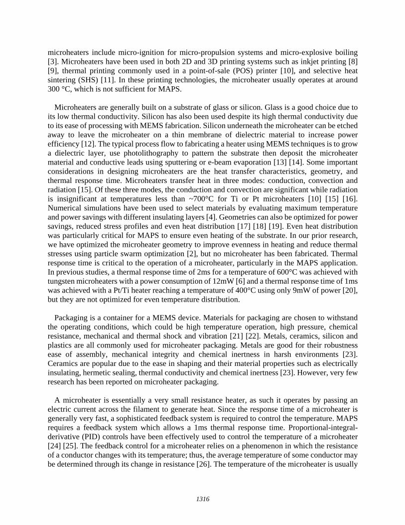
The die described above was manufactured using MEMS fabrication techniques. Photolithography followed by e-beam evaporation were used to deposit the microheater filaments and conductive leads. A more detailed description of the fabrication process is described below and shown in Figure 3:
Figure 3 – 2D and 3D representations of the fabrication steps of the microheater array: (a). the glass wafer is coated with a layer of photoresist; (b). the photoresist is exposed using the microheater mask and etched; (c). an adhesion layer of Ti followed by Pt filaments are deposited; (d). the photoresist is removed using acetone; (e). an adhesion layer of Ti followed by Au leads are deposited using the same procedure in steps (a) – (d).
1. A 500µm thick AF 32 eco glass wafer from Schott Inc. was used. 2. The wafer was cleaned using acetone and isopropyl alcohol, then rinsed with DI water
and dried. 3. AZ 5214-E photoresist was spin coated to a thickness of 2µm and prebaked. 4. UV photolithography was performed using the microheater mask, followed by post-
baking and a second blanket exposure. 5. The photoresist was etched using AZ MIF 300 developer. 6. E-Beam evaporation was used to deposit 100Å of titanium (adhesion layer) followed by
1500Å of platinum (heater filaments). 7. Lift-off of the photoresist and metal layer was achieved using acetone in an ultrasonic
bath. 8. A second photolithography stage identical to that previously mentioned was used to
pattern the wafer using the leads mask. 9. E-Beam evaporation was used to deposit 100Å of titanium followed by 1000Å of gold. 10. Lift-off of the photoresist and metal layer was achieved using acetone in an ultrasonic
bath. 11. The dies were cut using a dicing saw such that the gold leads extended to the edge of the
die.
After the heaters are fabricated onto the glass substrate, the wafer is diced into the individual heater dies, consisting of four microheaters each with two leads as shown in Figure 3. After dicing, it is possible to fabricate the extended leads, which are deposited via e-beam evaporation. The
1318

leads consist of an adhesion layer of titanium, followed by a layer of copper and finally a layer of tin, which is included to protect the copper from oxidation. The extended leads are fabricated onto these dies using the following steps, as shown in Figure 4:
1. Kapton tape was used to mask the sides of the dies in between each of the leads and to mask the top of the die where the microheaters are to avoid shorts between the leads.
2. The dies were put into a fixture to tilt them at a 45° angle such that both the side and top of the dies are exposed during evaporation.
3. E-beam evaporation was used to deposit 100Å of titanium followed by 1000Å of copper and finally another 100Å of tin to extend the leads to the sides of the die.
Figure 4 – Fabrication steps to extend leads. a. thin strips of Kapton tape are placed in between the leads and on top of the microheater array, b. the microheater dies are fixed at a 45° angle, c. extended copper leads are evaporated onto the top and sides of the microheater die.
3.2. Microheater Packaging The packaging of the microheater is an integral part to the success of MAPS. The packaging must accomplish the following tasks:
1. Provide a fixture of the heater die to the rest of the printer assembly; 2. Provide a method of electrical connection to the heaters; 3. Allow the microheaters to approach a flat substrate to a distance of ~2µm.
To satisfy these requirements, a basic QFN package was devised for the microheater die. The package is a two-layer printed circuit board (PCB) with an FR4 substrate, purple mask over bare copper, and ENIG finish. The package design can be seen in Figure 5.
Figure 5 - Top (left) and bottom (right) views of the packaging design for the microheater die
The extended side leads of the microheater die are bonded directly onto the conductive pads on the packaging using a silver epoxy – this allows for both electrical connection and a method of
1319

attachment between the die and the packaging. EPO-Tek® P1011 silver epoxy [29] was used to bond the heater die to the packaging using the following steps:
1. The microheater die is attached to the package using Kapton tape such that the leads on the die are aligned with the contact pads of the package.
2. The epoxy is manually applied using a needle such that it connects the individual leads to the contact pads (soldering can be used to replace epoxy in a production scenario).
3. A weight is placed on top of the die to ensure it stays in place, and the package is loaded into a vacuum oven to bake at 150°C for one hour to cure the epoxy.
4. The package is removed from the vacuum oven and the Kapton tape is removed. The finished packaging of the microheater die is shown in Figure 6.
Figure 6 - Finished microheater packaging with electrical connections and attachment accomplished with conductive epoxy
4. MICROHEATER TEMPERATURE CONTROL For MAPS, it is important to have precise control of the temperature of the microheater. Ideally,
the microheater should ramp to its target temperature of 400°C in 1ms and be maintained at that temperature until sintering is complete. It is also critical that the temperature of the microheater does not too far exceed the target temperature or else there is a risk of damaging the microheater. Because of these requirements, a sophisticated feedback control is needed.
The microheater temperature is controlled by a PID controller, a closed-loop control based on the temperature-resistivity relation of the microheater. Figure 7 illustrates the control loop of the microheater temperature. All data is processed by an 8-bit microcontroller board Arduino Mega. Arduino Mega generates an 8-bit data output which is converted to an analog voltage between 0 and 10 volts by a Digital to Analog Converter (DAC). The signal goes through the power amplifier to ensure that enough power will be delivered to the Wheatstone bridge where the microheater is connected. The voltage difference in the Wheatstone bridge between the Point A and Point B (Figure 8) is converted by the Analog to Digital Converter (ADC) and sent back to the Arduino Mega where the resistance of the Microheater is calculated. Based on the temperature-resistance relation, the temperature of the microheater is calculated and the control voltage output is updated to keep the microheater temperature around the target temperature.
1320

Figure 7 - Block diagram of the microheater control unit
Figure 8 - Microheater connected in the Wheatstone bridge
The microheater resistance Rm is calculated using three known resistors in the Wheatstone bridge as shown in the formula below:
𝑅𝑅𝑚𝑚 =
⎝
⎜⎛𝑅𝑅2 ∗ 𝑅𝑅3 + �𝑅𝑅3 ∗ (𝑅𝑅1 + 𝑅𝑅2) ∗ 𝐴𝐴𝐴𝐴𝐴𝐴 𝑉𝑉𝑉𝑉𝑉𝑉𝑉𝑉𝑉𝑉𝑉𝑉𝑉𝑉
𝐴𝐴𝐴𝐴𝐴𝐴 𝑉𝑉𝑉𝑉𝑉𝑉𝑉𝑉𝑉𝑉𝑉𝑉𝑉𝑉�
𝑅𝑅1 − �(𝑅𝑅1 + 𝑅𝑅2) ∗ 𝐴𝐴𝐴𝐴𝐴𝐴 𝑉𝑉𝑉𝑉𝑉𝑉𝑉𝑉𝑉𝑉𝑉𝑉𝑉𝑉𝐴𝐴𝐴𝐴𝐴𝐴 𝑉𝑉𝑉𝑉𝑉𝑉𝑉𝑉𝑉𝑉𝑉𝑉𝑉𝑉� ⎠
⎟⎞
(1)
5. EXPERIMENTAL RESULTS To use the circuit described in section 4, it is first required to determine the relationship between
temperature and resistance of the microheater. This was accomplished by loading the microheater into a furnace with a thermocouple and recording the resistance of the microheater at various temperatures. Platinum’s resistance changes linearly with changes in temperature [30], so a linear line of best fit was applied to the acquired data. The results of this test are shown in Figure 9.
1321
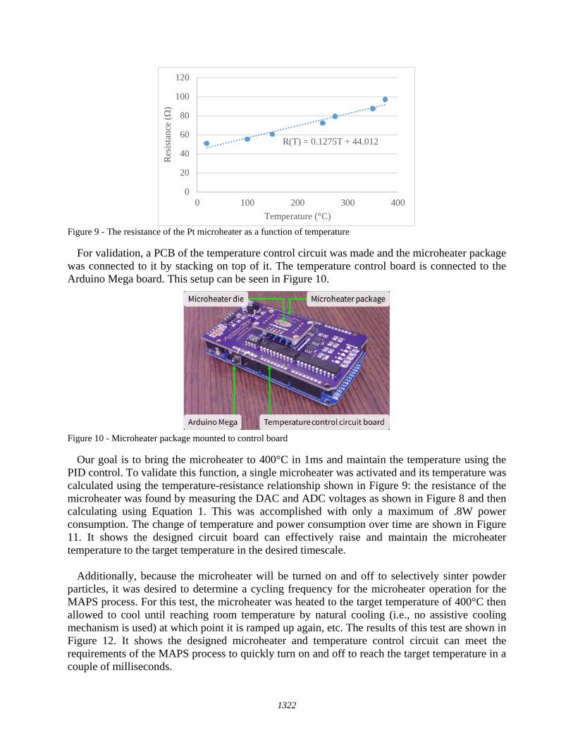
Figure 9 - The resistance of the Pt microheater as a function of temperature
For validation, a PCB of the temperature control circuit was made and the microheater package was connected to it by stacking on top of it. The temperature control board is connected to the Arduino Mega board. This setup can be seen in Figure 10.
Figure 10 - Microheater package mounted to control board
Our goal is to bring the microheater to 400°C in 1ms and maintain the temperature using the PID control. To validate this function, a single microheater was activated and its temperature was calculated using the temperature-resistance relationship shown in Figure 9: the resistance of the microheater was found by measuring the DAC and ADC voltages as shown in Figure 8 and then calculating using Equation 1. This was accomplished with only a maximum of .8W power consumption. The change of temperature and power consumption over time are shown in Figure 11. It shows the designed circuit board can effectively raise and maintain the microheater temperature to the target temperature in the desired timescale.
Additionally, because the microheater will be turned on and off to selectively sinter powder particles, it was desired to determine a cycling frequency for the microheater operation for the MAPS process. For this test, the microheater was heated to the target temperature of 400°C then allowed to cool until reaching room temperature by natural cooling (i.e., no assistive cooling mechanism is used) at which point it is ramped up again, etc. The results of this test are shown in Figure 12. It shows the designed microheater and temperature control circuit can meet the requirements of the MAPS process to quickly turn on and off to reach the target temperature in a couple of milliseconds.
R(T) = 0.1275T + 44.012
0
20
40
60
80
100
120
0 100 200 300 400
Res
ista
nce
(Ω)
Temperature (°C)
1322
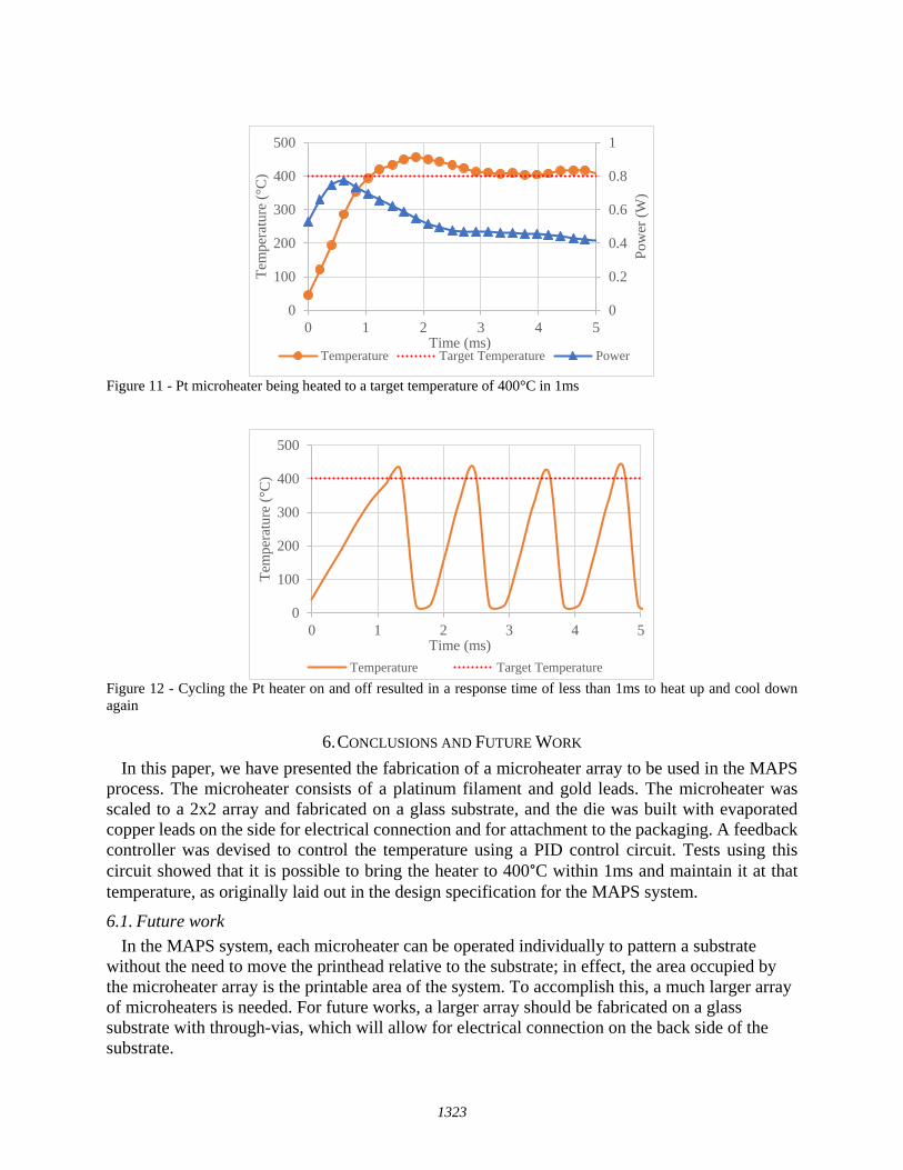
Figure 11 - Pt microheater being heated to a target temperature of 400°C in 1ms
Figure 12 - Cycling the Pt heater on and off resulted in a response time of less than 1ms to heat up and cool down again
6. CONCLUSIONS AND FUTURE WORK In this paper, we have presented the fabrication of a microheater array to be used in the MAPS
process. The microheater consists of a platinum filament and gold leads. The microheater was scaled to a 2x2 array and fabricated on a glass substrate, and the die was built with evaporated copper leads on the side for electrical connection and for attachment to the packaging. A feedback controller was devised to control the temperature using a PID control circuit. Tests using this circuit showed that it is possible to bring the heater to 400°C within 1ms and maintain it at that temperature, as originally laid out in the design specification for the MAPS system.
6.1. Future work In the MAPS system, each microheater can be operated individually to pattern a substrate
without the need to move the printhead relative to the substrate; in effect, the area occupied by the microheater array is the printable area of the system. To accomplish this, a much larger array of microheaters is needed. For future works, a larger array should be fabricated on a glass substrate with through-vias, which will allow for electrical connection on the back side of the substrate.
0
0.2
0.4
0.6
0.8
1
0 1 2 3 4 50
100
200
300
400
500
Pow
er (W
)
Time (ms)
Tem
pera
ture
(°C
)
Temperature Target Temperature Power
0 1 2 3 4 50
100
200
300
400
500
Time (ms)
Tem
pera
ture
(°C
)
Temperature Target Temperature
1323
7. ACKNOWLEDGEMENTS We gratefully acknowledge the financial support from the Oak Ridge Associated Universities
through the Ralph E. Powe Junior Faculty Enhancement Awards and from the University of Arkansas through the startup fund provided by the Vice Provost Office for Research and Economic Development. Errol Porter and Clint Hardee for their assistance in developing microheater array. Any opinions, findings, and conclusions or recommendations expressed in this publication are those of the authors and do not necessarily reflect the views of the University of Arkansas.
REFERENCES [1] A. Van Horn, "Selective Resistive Sintering: A Novel Additive Manufacturing Process," M.S. Thesis,
University of Arkansas, Fayetteville, 2016. [2] A. Van Horn and W. Zhou, "Design and optimization of a high temperature microheater for inkjet deposition,"
The International Journal of Advanced Manufacturing Technology, pp. 1-11, 2016. [3] K. L. Zhang, "Fabrication, modeling and testing of a thin film Au/Ti microheater," International Journal of
Thermal Sciences, vol. 46, no. 6, pp. 580-588, 2007. [4] S. Toskov, R. Glatz, G. Miskovic and G. Radosavljevic, "Modeling and fabrication of pt micro-heaters built
on alumina substrate," in 36th International Spring Seminar On Electronics Technology, 2013. [5] R. M. Tiggelaar, "Silicon-technology based microreactors for high-temperature heterogeneous partial
oxidation reactions," M.S. Thesis, University of Twente, Enschede, The Netherlands, 2004. [6] S. Z. Ali, F. Udrea, W. I. Milne and J. W. Gardner, "Tungsten-based SOI microhotplates for smart gas
sensors," Journal of Microelectromechanical Systems, vol. 17, pp. 1408-1417, 2008. [7] L. Mele, F. Santagata and E. Iervolino, "A molybdenum MEMS microhotplate for high-temperature
operation," Sensors and Actuators A: Physical, vol. 188, pp. 173-180, 2012. [8] L. Setti, C. Piana and S. Bonazzi, "Thermal inkjet technology for the microdeposition of biological molecules
as a viable route for the realization of biosensors," Anal. Lett., vol. 37, pp. 1559-1570, 2004. [9] X. Cui and T. Boland, "Human microvasculature fabrication using thermal inkjet printing technology,"
Biomaterials, vol. 30, pp. 6221-6227, 2009. [10] T. Mendum, E. Stoler, H. VanBenschoten and J. C. Warner, "Concentration of bisphenol A in thermal paper,"
Green Chemistry Letters and Reviews, vol. 4, pp. 81-86, 2011. [11] M. Baumers, C. Tuck and R. Hague, "SELECTIVE HEAT SINTERING VERSUS LASER SINTERING:
COMPARISON OF DEPOSITION RATE, PROCESS ENERGY CONSUMPTION AND COST PERFORMANCE".
[12] L. Xu, Y. Wang and H. Zhou, "Design, Fabrication, and Characterization of a High-Heating-Efficiency 3-D Microheater for Catalytic Gas Sensors," Journal of Microelectromechanical Systems, vol. 21, no. 6, pp. 1402-1409, 2012.
[13] W.-Y. Chang and Y.-S. Hsihe, "Multilayer microheater based on glass substrate using MEMS technology," Microelectronic Engineering, vol. 149, pp. 25-30, 2016.
[14] T. Guan and R. Puers, "Thermal Analysis of a Ag/Ti Based Microheater," Procedia Engineering, vol. 5, pp. 1356-1359, 2010.
[15] A. Pike and J. W. Gardner, "Thermal modelling and characterisation of micropower chemoresistive silicon sensors," Sensors and Actuators B: Chemical, vol. 45, pp. 19-26, 1997.
[16] D. Bradley and A. Entwistle, "Determination of the emissivity, for total radiation, of small diameter Platinum-10% Rhodium wires in the temperature range 600-1450 C," British Journal of Applied Physics, vol. 12, p. 708, 1961.
1324
[17] S. Joy and J. K. Antony, "Design and simulation of a micro hotplate using COMSOL multiphysics for MEMS based gas sensor," in Fifth International Conference on Advances in Computing and Communications (ICACC), 2015.
[18] G. Velmathi, S. Ramshanker and S. Mohan, "Design, electro-thermal simulation and geometrical optimization of double spiral shaped microheater on a suspended membrane for gas sensing," in 36th Annual Conference on IEEE Industrial Electronics Society, 2010.
[19] S. Lee, D. Dyer and J. Gardner, "Design and optimisation of a high-temperature silicon micro-hotplate for nanoporous palladium pellistors," Microelectronics Journal, vol. 34, pp. 115-126, 2003.
[20] Y. Mo, Y. Okawa, K. Inoue and K. Natukawa, "Low-voltage and low-power optimization of micro-heater and its on-chip drive circuitry for gas sensor array," Sensors and Actuators A: Physical, vol. 100, pp. 94-101, 2002.
[21] J. Köhler, K. Jonsson, M. Jönsson, L. Stenmark and Y. Bäcklund, "Space qualification of direct bonded silicon microsystems," in Micro Nano Technology for Space Applications, Pasadena, CA, 2000.
[22] J. Connelly, A. Kourepenis, D. Larsen and T. Marinis, "Inertial MEMS Development for Space," in 2nd international conference on integrated Micro/Nanotechnology for Space Applications, 1999.
[23] N. Maluf and K. Williams, Introduction to Microelectromechanical Systems Engineering, Artech House, 2004.
[24] B. Bae, J. Yeom, B. R. Flachsbart and M. A. Shannon, "A Sensorless and Versatile Temperature-Control System for MEMS Microheaters," Transactions of the Korean Institute of Electrical Engineers, vol. 55, no. 11, pp. 544-547, 2006.
[25] M. N. H. Z. Alam, A. A. A. Moghadam and A. Kouzani, "Establishment of temperature control scheme for microbioreactor operation using integrated microheater," Microsystem Technologies, vol. 21, no. 2, pp. 415-428, 2015.
[26] J. F. Creemer, D. Briand and H. W. Zandbergen, "Microhotplates with TiN heaters," Sensors and Actuators A: Physical, vol. 148, no. 2, pp. 416-421, 2008.
[27] "AF 32 Thin Glass," [Online]. Available: http://www.schott.com/d/advanced_optics/5b420dd5-2a84-4c81-98e4-9efdcc011e61/1.0/schott-af-32-eco-thin-glass-may-2013-eng.pdf. [Accessed 16 March 2017].
[28] "Schott HermeS - Hermetic Through Glass Vias (TGV)," [Online]. Available: http://www.schott.com/d/epackaging/16cda2bd-dff5-4041-8b6e-7631bc076505/1.0/schott-hermes-hermetic-through-glass-vias-datasheet_en.pdf. [Accessed 16 March 2017].
[29] EPOXY TECHNOLOGY, INC., "EPO-TEK P1011 Technical Data Sheet," [Online]. Available: http://www.epotek.com/site/administrator/components/com_products/assets/files/Style_Uploads/P1011.pdf. [Accessed 13 April 2017].
[30] "Thermophysical Data on Platinum," Platinum Metals Review, vol. 28, no. 4, p. 164, 1984. [31] HP Development Company, L.P., "Timeline of our history," 2017. [Online]. Available:
http://www8.hp.com/us/en/hp-information/about-hp/history/hp-timeline/timeline.html. [Accessed 30 March 2017].
[32] M. Baroncini, P. Placidi, G. C. Cardinali and A. Scorzoni, "Thermal characterization of a microheater for micromachined gas sensors," Sensors and Actuators A, vol. 115, no. 1, pp. 8-14, 2004.
[33] J. Puigcorbé, D. Vogel and B. Michel, "Thermal and mechanical analysis of micromachined gas sensors," Journal of Micromechanics and Microengineering, vol. 13, no. 5, pp. 548-556, 2003.
1325