Embed Size (px)
Citation preview

Fabrication and Characterization of Schottky Diodes and MOS Capacitors [Module 5] Authors Names
Introduction and Background: The characterization of Schottky diodes and MOS capacitors are common techniques used to gain a better understanding of a device performance which can lead to changes in processes to improve yield, or performance of a device. A Schottky diode is similar to the pn-diode except that it takes a lower threshold voltage to turn on (or to forward bias the diode) and has quicker switching capabilities.
Fig. 1 Schottky curves showing the current and voltage relationship. [1]
A Schottky barrier when reversed biased causes the barrier energy to increase thus preventing the flow of electrons across the device. A Schottky barrier that is forward biased causes the barrier energy to decrease thus allowing current to flow across the device.

Fig 2. Schottky barrier band diagram. [2]
Fig 3. Capacitance vs voltage curve of metal insulator semiconductor (MOS capacitor) [2] One of the main reasons for taking a CV measurement in the lab is to characterize the threshold voltage or the inversion layer when the gate voltage is applied since the gate structure is similar to a capacitor physically. The IV measurement can show the device response, whether it is linear like an ohmic device or non linear. Methods:
The first step was to use the mask aligner. We already came into this set up with wafers that had a mask on them. The first step was to spin photoresist on top of the existing dry oxide that was our mask. 1813 positive photoresist was used and the spin speed was set to 5000 rpm for 45 seconds. The photoresist is applied so that when the mask is exposed to the light, only the portions not under the mask will develop off of our samples. This is an example of positive photoresist, whereas negative photoresist would have the opposite effect. The samples were

then soft baked for 45 seconds. The purpose of the soft bake is to remove internal stresses caused by the spin process, ensure adhesion to the sample, and remove any solvents prior to exposing. After this was complete the mask was placed in the mask aligner and the sample was aligned to the mask. In the case of some of the samples this had to be done by sight as they had no identifying marks. The other set of samples were aligned using straight features and edges of the mask both on the transparency and the sample. The samples were then exposed for 35 seconds. After the exposure the samples were developed for one minute and hard baked for 90 seconds. The developer solution removed the photoresist not covered by the mask when exposed. This also removed the oxide layer underneath the photoresist leaving only the oxide layer matching the mask. The hard bake is similar to the soft bake in that it ensures strength in the sample and removes solvents. Finally, the samples were placed in BOE for a short rinse to rid the sample of any unwanted oxide. The BOE etch was complete when the samples were hydrophobic.The remaining photoresist was then removed with acetone followed by a methanol rinse. The samples were then dried and continued on to the metallization step. The photoresist, mask aligning, process is important when developing a MOSFET because the procedure will have to be done three separate times in order to have levels of different patterns. MOSFETS are more complicated in structure and require metal contacts on oxides and off as well as different structures on different doped regions.
The samples went through a thin film deposition process applying aluminium on the back side of the wafer and copper circles to the front side of the wafer with the masked oxide pattern. The reasoning behind this is so the samples could be characterized with contacts on oxide and contacts off of oxide. To deposit materials a thin film system was used with a mechanical pump and diffusion pump. Prior to bringing the system under vacuum, the metal being deposited is placed in a coil connected in circuit to have high current flowing through it. The reasoning behind this is so the coil heats up and the material starts to evaporate. The chamber being low vacuum helps with the evaporation process as well. When the metal was placed in the coil, the sample was placed above it in preparation for deposition. The chamber was then sealed and brought to low vacuum with a mechanical pump. Once an adequate pressure of around 1x10^-3 torr was reached, the diffusion pump was turned on. This pump requires a backing pump while operating, so the mechanical pump was switched to back the diffusion pump. The chamber was then brought down to the 1x10^-5 and lower range before turning on the current. A Quartz Crystal Monitor (QCM) was used to measure the thickness being deposited. The desired thickness was 500-800 Angstroms. Once this was achieved, the metal was switched out for copper and the samples were flipped over to deposit on the opposite side and placed on a shadow mask to only deposit circles. The deposition process was repeated, again aiming for 500-800 Angstroms. The metallization process is important for developing a MOSFET because the Gate, Source, and Drain have to be deposited onto the MOSFET at specific thicknesses in order to be effective.
After the samples had metal contacts, a series of IV (current and voltage) and CV (capacitance and voltage) measurements were made. The copper on bare silicon contacts model a schottky diode while the copper on oxide contacts model a MOS structure. Characterization like this will develop understanding of schottky, MOS, and contact to contact physics and especially help when troubleshooting the creation of a MOSFET.

Results: As mentioned above, current-voltage (I-V) characteristics were measured for each of the three combinations of contacts available on the oxidized, patterned Si wafers. These combinations were 1.) Cu contact on bare Si to Al back contact, 2.) Cu contact on SiO2 to Al back contact, and 3.) Cu on bare Si to Cu on SiO2. Several measurements were taken for each combination by switching which Cu pads were used for the front contact (or which Cu pads were used for both front and back contacts, in case 3.). Representative I-V characteristics for each contact combination are plotted together in Figure 4, below.
Figure 4: I-V characteristics for each of three contact combinations. The MOS capacitor (blue trace) corresponds to case 2, the Schottky barrier (black trace) corresponds to case 1, and the
double diode (green trace) corresponds to case 3.
Additionally, capacitance-voltage (C-V) characteristics were measured for the Schottky barrier diode (case 1) and the MOS capacitor (case 2). The C-V characteristic for the Schottky barrier was measured in forward and reverse bias. Representative C-V characteristics are given below in Figures 5 and 6.

Figures 5 and 6: Figure 5 (left plot) gives the forward and reverse bias C-V characteristics for
the Schottky barrier configuration described in case 1, above. Figure 6 (right plot) gives the C-V characteristic for the MOS capacitor configuration described in case 2, above.
Discussion and Conclusions: I-V Characteristics The measured I-V characteristic for the MOS capacitor (blue trace in Figure 4) exhibits rather clean behavior compared to what would be expected for a trial, student-fabricated device structure. There is no leakage current except for voltages less than -4 V, at which point an almost discontinuous drop from zero current is observed, preceded by a flat current profile. If this region had exhibited not a flat profile, but instead an exponential or more linear drop, it would have been reasonable to assume that the voltage where the drop occurred was the breakdown voltage. The breakdown voltage, in this case, describes the critical voltage at which the insulating oxide layer would become conductive. However, the current profile in this region drops abruptly, preceded by a flat current-voltage relationship. This feature is most likely an artifact of the measurement apparatus, which is highly sensitive to vibrations and was found to have at least one loose electrical connection. This conclusion is further supported because this almost discontinuous drop was not reproducible from measurement to measurement of the same device, while similar features were seen in measurements of completely different device structures. As can be seen in Figure 4, the turn on voltage for the MOS capacitor is about 1.97 V, and behaves Ohmically soon after reaching the turn on voltage. This I-V profile agrees well with examples from the literature, and makes intuitive sense since the MOS capacitor is nothing more than a resistive load the current flows through after the turn on voltage is surpassed. The I-V characteristic for the Schottky barrier diode (black trace in Figure 4) exhibits leakage current in the negative voltage sweep regime. This leakage current increases linearly with voltage (Ohmic behavior), as would be expected for a resistor. Based on this observation, it can be concluded that some sort of shunt existed in the device structure. Furthermore, the turn

on voltage observed for the Schottky barrier is far less than the turn on voltage for the MOS capacitor, at just above 0 V for the Schottky barrier. The consequence of this feature is that less power can be pushed through the Schottky circuit as compared to the MOS circuit. Finally, the I-V characteristic is once again Ohmic after the turn on voltage for the same reason as given above for the MOS structure. The most interesting I-V characteristic was collected when the instrument leads were placed on two Cu contacts on the front of the patterned wafer; one contact on bare Si and one contact on SiO2. This configuration is equivalent to having two MOS capacitors in series, since it can be assumed that a native oxide of a few nanometers was present on the bare Si surface before depositing the contacts. That being said, the “Double Diode” curve noted in Figure 4 (green trace) corresponds to a true MOS capacitor on the right hand side of the plot and a leaky MOS capacitor on the left hand side of the plot. The right hand side of the green trace in Figure 4 clearly exhibits a linear I-V regime followed by saturation (flat portion). The left hand side of the green trace in Figure 4 looks similar to the right hand side, except that it does not level off after reaching saturation, therefore it must be experiencing some sort of leakage current, as well. C-V Characteristics The C-V characteristic shown in Figure 5 gives the forward and reverse bias voltage sweeps for a representative Schottky barrier diode (case 2 described above for Figure 4). Both forward and reverse bias curves terminate at roughly the same value of current, ~1.46E-6 to 1.49E-6 A. Again, this result is surprising given that these devices were fabricated on a trial basis in a student laboratory. The most important difference observed between forward and reverse bias for this plot is that in reverse, the Schottky barrier does not appear to reach saturation, and instead becomes linear as the voltage is increased. This is again, indicative of some sort of shunt in the device structure. In Figure 6, the C-V characteristic for a representative MOS capacitor is given, and displays two important features. First, the threshold voltage at which inversion is created can be read from the plot where the I-V curve drops; a voltage of about 1.5 V. Second, the I-V curve never quite flattens out at the high voltage extreme. This sort of feature is indicative of sweeping the voltage too quickly, such that the device structure cannot reached equilibrium before the voltage changes again [4].
Fabrication and Characterization of Ohmic Contacts and pn-Diodes [Module 6] Authors Names
Methods: The next set of steps began with quarter wafers that dopant had been spun onto. There were both phosphorous doped (n-type) and boron doped (p-type) quarters. The doping process utilizes the same device for spinning on photoresist. The settings were set to not spin while dopant was added, spin at 500 RPM for 9 seconds, then ramp up to 3000 RPM for 20 seconds.

Applying dopants is important to the construction of a MOSFET because a MOSFET is composed of and operates based on pn junctions.
Since the wafers had sat for over a week the wafers were briefly submerged in a 10% HF strip solution in order to strip the native oxide from the surface. We could be sure that the native oxide was removed by noting the hydrophobicity of the surface. The wafers were then rinsed in deionized water and blown dry with nitrogen. The next phase in the creation of ohmic contacts included thermal evaporation of aluminum onto the back of the wafers. This allowed for creation of a back contact. The thermal evaporation procedure consisted of a start up of the system that allowed the vacuum chamber to be pumped down to the desired pressure. The chamber was first roughed out to about 100 mtorr. The bell jar cavity in which the thermal evaporation would take place was then exposed to a diffusion pump which brought it down to about 4e-6 torr. A filament was then used to track the rate of deposition of the aluminum. When the total thickness reached between 500 and 800 angstroms the first evaporation phase was complete. We then characterized the thickness of the aluminum using a profilometer in order to verify the measurement given by the filament. The wafers were then flipped over so that the polished, doped surface would be the deposition surface. A shadow mask was placed between the wafers and the deposition material so that dots of aluminum would be deposited on the surface of the wafer. This would give several contacts with which to take data. These were once again made to be 500 to 800 angstroms thick.
The next step was to characterize the contacts. I-V curves were taken between two dots as well as one dot and the back contact. Several dots were tested in order to provide sufficient data.
Once this characterization was complete the samples were placed in a plasma etch with the dots face up. The etch was carried out using SF6 as aluminum does not etch much in this compound. This allowed for the silicon around the aluminum dots to be etched, creating mesas of aluminum. The etch pressure was 250 mtorr and the power was set to 200 W. The gas flow rate was set to stabilize the desired pressure.Etch time was set to 15 seconds. The wafers were then tested in the same manner as the first characterization, with an I-V curve, to see if the ohmic behavior remained. If it did the samples were placed in the plasma etch for another 15 seconds until this behavior ceased to exist in the p-type quarters.
The final step of this procedure was to characterize several combinations of dots and back contacts using I-V and C-V measurements. The p-type samples were focused on as they were the ones that had a characterization change in terms of I-V curves. The C-V data was taken for a range of voltages within the expected breakdown voltage of the sample. These curves were used to obtain a diode doping level. Homogeneity as well as depth and size of the depletion region were analyzed from this data. Results and Discussion: Profilometry measurements on the Aluminum contacts deposited on the back of the substrates determined the thickness of those contacts to be 60 nm. During deposition of the front contacts
(Aluminum dots), the boat holding the aluminum broke which caused the thickness of those contacts to be 27 nm as determined by profilometer measurements as well.
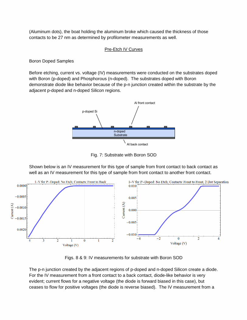
Pre-Etch IV Curves Boron Doped Samples Before etching, current vs. voltage (IV) measurements were conducted on the substrates doped with Boron (p-doped) and Phosphorous (n-doped). The substrates doped with Boron demonstrate diode like behavior because of the p-n junction created within the substrate by the adjacent p-doped and n-doped Silicon regions.
Fig. 7: Substrate with Boron SOD
Shown below is an IV measurement for this type of sample from front contact to back contact as well as an IV measurement for this type of sample from front contact to another front contact.
Figs. 8 & 9: IV measurements for substrate with Boron SOD
The p-n junction created by the adjacent regions of p-doped and n-doped Silicon create a diode. For the IV measurement from a front contact to a back contact, diode-like behavior is very evident; current flows for a negative voltage (the diode is forward biased in this case), but ceases to flow for positive voltages (the diode is reverse biased). The IV measurement from a

front contact to another front contact demonstrates the behavior similar to two diodes in a ring as shown in Figure 10 below.
Fig. 10: Diode ring and corresponding IV curve [3] The front to front contacts have this associated IV curve because electrons are able to flow through the p-doped regions between front contacts. Phosphorous Doped Samples As could be expected, when the originally n-doped Silicon substrate was doped with additional n-type dopant (Phosphorous SOD), this led to linear IV curves for both the measurement from a front contact to the back contact and the measurement from a front contact to another front contact (Figs. 11 and 12).
Figs. 11 & 12: IV measurements for substrate with Phosphorous SOD

This behavior is expected because of the lack of any p-n junction. In these cases, the aluminum contacts are ohmic in nature.
Post-Etch IV Curves During the SF6 etch, the front Aluminum contacts remained relatively unscathed, while the Silicon was partially etched away leaving columns of material composed of Aluminum and either p-doped Silicon or strongly n-doped Silicon as shown in Figure 13.
Fig 13: Post-Etch Substrate Boron Doped Samples What the etching should have done was eliminate the path between front contacts that electrons were able to take previously before the etch: the path through either the n+-doped region or the p-doped region. When taking IV measurements then, in order to get from a front contact to another front contact, electrons would have to travel through back to back diodes and the IV curve would look similar to (b) in the graph of Figure 10. Unfortunately, either due to uneven etching of Silicon, incomplete etching through the doped layer of Silicon, or perhaps too thin of Aluminum front contacts, ohmic behavior was measured for the Boron doped samples between front Aluminum contacts as shown in Figure 14. As before the etch, IV measurements between front and back contacts lead to diode-like behavior as shown in Figure 15.

Figs. 14 & 15: IV curves for post-etch Boron doped substrate
A longer etch time would almost surely remedy this inconsistency between our experimental results with expected, theoretical behavior Phosphorous Doped Samples Behavior similar to that observed with the Boron doped samples was also observed with the Phosphorous doped samples. Due to incomplete etching through the n+-doped layer, ohmic behavior was still observed when IV measurements were taken between front contacts. What was expected would again be similar to curve (b) in the graph of Figure 10. However, instead of the back to back diode like behavior being caused by p-n junction diodes as for the Boron doped samples, the diodes involved with the Phosphorous doped samples are Schottky Barrier diodes (diodes forming from metal-semiconductor junctions). Post-etch IV curves for the Phosphorous doped samples are shown in Figures 16 and 17.

Figs. 16 & 17: IV curves for post-etch Phosphorous doped substrate
Again, during the IV measurements, ohmic contacts were observed between front contacts due to an incomplete etch of the n+-doped layer, while Schottky-barrier diode-like behavior was observed between front and back contacts
Post-Etch C-V Curves
Varying the voltage across a p-n junction varies the depletion width of the junction. The depletion region is devoid of conducting electrons and holes but ionized donors are left behind which behave identically to a capacitor. When the depletion region changes, so does the capacitance of the junction (diode device). This is what is being measured in this section. Boron Doped Samples Increasing the voltage across a p-n junction increases the width of the depletion region which is in turn increasing the distance between ionized donor areas. This is identical to increasing the distance between capacitor plates which reduces the capacitance of the capacitor. As seen in Figure 18, this is exactly the type of behavior that was observed during the experiment.

Fig. 18: CV curve for post-etch, Boron doped substrate Phosphorous Doped Samples The capacitance for the n+-doped samples decreased then increased as voltage increased across the metal-semiconductor junction. This must be caused by an increase in distance of the region similar to the depletion region for p-n junctions. As the voltage increases, there is a larger increase in charge buildup which then increases capacitance due to the C = dQ/dV relationship.
Fig. 19: CV curve for post-etch, Boron doped substrate References [1] Mpulse Microwave, “Schottky curves”, http://www.mpulsemw.com/SchottkyDiode.htm

[2] David Sebastiao Cabral, Robson Luiz Moreno, Tales Cleber Pimenta, Leonardo Breseghello Zoccal and Paulo Cesar Crepaldi, “Implementation of Schottky Barrier Diodes (SBD) in Standard CMOS Process for Biomedical Applications”, Universidade Federal de Itajuba, Brasil, http://www.intechopen.com/books/biomedical-engineering-technical-applications-in-medicine/implementation-of-schottky-barrier-diodes-sbd-in-standard-cmos-process-for-biomedical-applications
[3] http://www.wtec.org/loyola/displays/c3_s3.htm [4] Keithley Application Note Series, Number 2239, copyright 2006.