Embed Size (px)
Citation preview

University of Kentucky University of Kentucky
UKnowledge UKnowledge
University of Kentucky Master's Theses Graduate School
2005
Fabrication and Characterization of Schottky diode and Fabrication and Characterization of Schottky diode and
Heterojunction Solar cells based on Copper Phthalocyanine Heterojunction Solar cells based on Copper Phthalocyanine
(CuPc), Buckminster Fullerene (C60) and Titanium Dioxide (TiO2) (CuPc), Buckminster Fullerene (C60) and Titanium Dioxide (TiO2)
Subhash C. C. Vallurupalli University of Kentucky
Right click to open a feedback form in a new tab to let us know how this document benefits you. Right click to open a feedback form in a new tab to let us know how this document benefits you.
Recommended Citation Recommended Citation Vallurupalli, Subhash C. C., "Fabrication and Characterization of Schottky diode and Heterojunction Solar cells based on Copper Phthalocyanine (CuPc), Buckminster Fullerene (C60) and Titanium Dioxide (TiO2)" (2005). University of Kentucky Master's Theses. 260. https://uknowledge.uky.edu/gradschool_theses/260
This Thesis is brought to you for free and open access by the Graduate School at UKnowledge. It has been accepted for inclusion in University of Kentucky Master's Theses by an authorized administrator of UKnowledge. For more information, please contact [email protected].
Abstract of Thesis
Fabrication and Characterization of Schottky diode and Heterojunction
Solar cells based on Copper Phthalocyanine (CuPc), Buckminster
Fullerene (C60) and Titanium Dioxide (TiO2)
Organic solar cells are cheaper and much easier to fabricate than the conventional
inorganic solar cells, but they suffer from low efficiencies due to low carrier mobilities in
organic films. In this study Copper Phthalocyanine (CuPc) and Buckminster Fullerene
(C60) based Schottky diodes were fabricated on ITO coated glass substrates to study their
performance and a study of the effect of thickness on the cell parameters of CuPc
Schottky diodes was made. Also, TiO2 based devices were studied to see the effect of
TiO2 layer on the cell parameters. The J-V curves were analyzed for series resistance,
diode ideality factor and reverse saturation current density. The devices were also
characterized by SEM and XRD measurements.
KEYWORDS: C60 , CuPc, TiO2, Schottky diode solar cells, Heterojunction solar cells.
Subhash C. C. Vallurupalli Author’s Signature
September 18, 2005
Date
FABRICATION AND CHARACTERIZATION OF SCHOTTKY DIODE AND HETEROJUNCTION SOLAR CELLS BASED ON COPPER
PHTHALOCYANINE (CuPc), BUCKMINSTER FULLERENE (C60) AND TITANIUM DIOXIDE (TiO2)
By
Subhash C. C. Vallurupalli
Dr. Vijay P. Singh -------------------------------------------
(Director of Thesis)
Dr. YuMing Zhang -------------------------------------------
(Director of Graduate Studies)
------------------------------------------- (Date)
Copyright © Subhash C. C. Vallurupalli 2005
RULES FOR THE USE OF THESES
Unpublished theses submitted for the Master’s degree and deposited in the University of Kentucky Library are as a rule open for inspection, but are to be used only with due regard to the rights of the authors. Bibliographical references may be noted, but quotations or summaries of parts may be published only with the permission of the author, or with the usual scholarly acknowledgements. Extensive copying or publication of the thesis in whole or in part also requires the consent of the Dean of the Graduate School of the University of Kentucky. A library that borrows this dissertation for use by its patrons is expected to secure the signature of each user. Name Date
THESIS
Subhash C. C. Vallurupalli
The Graduate School
University of Kentucky
2005
FABRICATION AND CHARACTERIZATION OF SCHOTTKY DIODE AND HETEROJUNCTION SOLAR CELLS BASED ON COPPER
PHTHALOCYANINE (CuPc), BUCKMINSTER FULLERENE (C60) AND TITANIUM DIOXIDE (TiO2)
THESIS
A thesis submitted in partial fulfillment of the requirements for the degree of Master of Science in the
College of Engineering at the University of Kentucky
By
Subhash C. C. Vallurupalli
Lexington, Kentucky
Director: Dr. Vijay P. Singh, Professor & Chair
Electrical and Computer Engineering
Lexington, Kentucky
2005
Copyright © Subhash C. C. Vallurupalli 2005
MASTER’S THESIS RELEASE
I authorize the University of Kentucky
Libraries to reproduce this thesis in
whole or in part for the purpose of research.
SIGNED: __________________________
DATE: __________________________

iii
ACKNOWLEDGEMENTS
I thank Dr. Vijay P. Singh from the bottom of my heart for having given me a chance to be a
part of this research. I am deeply obliged to Dr. J. Todd Hastings and Dr. Ingrid St. Omer for
having agreed to be on my Thesis Committee. They have provided outstanding insights that have
guided me to deliver a much better work. Their critical review is gratefully acknowledged.
It is only the unparalleled love, support and vision of my parents that has made this work a
reality. I would like to thank Dr. Suresh Rajaputra for all his help in this work and for guiding me
to solve most of the problems I faced. I would like to thank all my friends who have understood
and motivated me during the course of this work. It is their unconditional love that has sustained
me through the last couple of years.

iv
Table of Contents
ACKNOWLEDGEMENTS ---------------------------------------------------------------
List of Tables --------------------------------------------------------------------------------
List of Figures --------------------------------------------------------------------------------
List of Files ----------------------------------------------------------------------------------
Chapter 1. Introduction ------------------------------------------------------------------
1.1 Purpose --------------------------------------------------------------------------------
1.2 A brief history of solar cells ------------------------------------------------------
1.3 Current trends with solar cells --------------------------------------------------
1.4 C60 based Schottky diode solar cells --------------------------------------------
1.5 CuPc based Schottky diode solar cells ------------------------------------------
1.6 TiO2/CuPc heterojunction solar cells -------------------------------------------
Chapter 2. Theory ------------------------------------------------------
2.1 Theory of Schottky diode solar cells --------------------------------------------
2.2 Theory of heterojunction solar cells --------------------------------------------
2.3 Principles of operation of organic solar cells ---------------------------------
2.4 Equivalent circuit of a solar cell -----------------------------------------------
2.5 Photovoltaic parameters ----------------------------------------------------------
2.5.1 Short circuit current --------------------------------------------------------
2.5.2 Open circuit voltage ------------------------------------------------------------
2.5.3 Maximum power output ------------------------------------------------------
2.5.4 Fill Factor ------------------------------------------------------------------------
2.5.5 Efficiency -----------------------------------------------------------------------
Chapter 3. Experimental -------------------------------------------------------------------------
3.1 Device fabrication ------------------------------------------------------------------
3.1.1 Device structures -------------------------------------------------------------
3.1.2 Preparation of TiO2 sol-gel --------------------------------------------------
3.1.3 Substrate cleaning -------------------------------------------------------------
3.1.4 Spin coating of the PEDOT:PSS film for device structures 1 and 2
3.1.5 Spin coating of the TiO2 sol-gel for device structures 3 and 4 -------
3.1.6 Fabrication of C60 films ----------------------------------------------------
iii
vii
viii
xiv
1
1
1
2
2
3
3
5
5
8
9
12
13
13
13
13
14
14
15
15
15
18
18
18
19
19
v
3.1.7 Fabrication of CuPc films ---------------------------------------------------
3.1.8 Fabrication of PTCBI films -------------------------------------------------
3.1.9 Deposition of Aluminium contacts -----------------------------------------
3.2 X-ray Diffraction (XRD) ------------------------------------------------------------
3.3 Field Emission Scanning Electron Microscope (FE-SEM) Imaging --------
3.3.1 Sample Preparation -----------------------------------------------------------
3.3.2 Specimen Exchange ----------------------------------------------------------
3.3.3 SEM Imaging -------------------------------------------------------------------
3.4 Optical Absorption ------------------------------------------------------------------
3.4.1 Measurement of Spectrum -------------------------------------------------
3.5 I-V Measurement Setup ----------------------------------------------------------
Chapter 4. Material Characterization ------------------------------------------------
4.1 Characterization of C60 by SEM --------------------------------------------------
4.2 Characterization of C60 by XRD --------------------------------------------------
4.3 Characterization of CuPc by SEM -----------------------------------------------
4.4 Characterization of CuPc by XRD ------------------------------------------------
4.5 Characterization of TiO2 by SEM -----------------------------------------------
Chapter 5. Optical Characterization -----------------------------------------------------
5.1 Optical absorption of C60 ------------------------------------------------------------
5.2 Calculation of Absorption coefficient (α) -----------------------------------------
5.3 Optical absorption of CuPc film of thickness 15 nm ---------------------------
5.4 Optical absorption of CuPc film of thickness 60 nm ---------------------------
5.5 Optical absorption of CuPc film of thickness 80 nm ---------------------------
5.6 Optical absorption of CuPc film of thickness 100 nm -----------------------
5.7 Optical absorption of CuPc film of thickness 120 nm -----------------------
5.8 Optical absorption of CuPc film of thickness 140 nm -------------------------
5.9 Comparision of optical absorption of CuPc films of thickness 15, 60,
80, 100, 120 and 140 nm ---------------------------------------------------------------
5.10 Optical absorption of 4 times spin coated TiO2 film of thickness 30 nm-
5.11 Optical absorption of CuPc(15 nm) on top of 4 times spin coated
TiO2 film of thickness 30 nm ------------------------------------------------------
19
20
20
20
21
21
22
22
22
23
23
25
25
26
27
28
29
31
31
31
32
34
35
36
37
39
40
42
43
vi
Chapter 6. Electrical Characterization ------------------------------------------------
6.1 J-V Characteristics -------------------------------------------------------------------
6.2 Series Resistance (Rs) -----------------------------------------------------------------
6.3 Ideality Factor (n) and Reverse Saturation Current Density (Jo) ----------
6.4 J-V characteristics of C60(40 nm)/Al Schottky diode solar cell ---------------
6.5 J-V characteristics of C60(60 nm)/Al Schottky diode solar cell --------------
6.6 J-V characteristics of CuPc/Al Schottky diode solar cells -------------------
6.6.1 J-V characteristics of CuPc(15 nm)/Al device -----------------------------
6.6.2 J-V characteristics of CuPc(60 nm)/Al device -----------------------------
6.6.3 J-V characteristics of CuPc(80 nm)/Al device -----------------------------
6.6.4 J-V characteristics of CuPc(100 nm)/Al device ---------------------------
6.6.5 J-V characteristics of CuPc(120 nm)/Al device ---------------------------
6.6.6 J-V characteristics of CuPc(140 nm)/Al device --------------------------
6.7 J-V characteristics of TiO2 based solar cell --------------------------------------
6.7.1 J-V characteristics of Glass/ITO/TiO2/CuPc/Al device -----------------
6.7.2 J-V characteristics of Glass/ITO/TiO2/CuPc/PTCBI/Al device ------- -
Chapter 7. Discussion ---------------------------------------------------------------------
7.1 Material characterization of C60 -----------------------------------------------
7.2 Optical characterization of C60 --------------------------------------------------
7.3 Electrical characterization of C60 based Schottky diode solar cells
7.4 Material characterization of CuPc ---------------------------------------------
7.5 Optical characterization of CuPc ----------------------------------------------
7.6 Electrical characterization of CuPc based Schottky diode solar cells
7.7 Material characterization of TiO2 -----------------------------------------------
7.8 Optical characterization of TiO2 ----------------------------------------------
7.9 Electrical characterization of ITO/TiO2/CuPc/Al and ITO/TiO2/
CuPc/PTCBI/Al solar cells ------------------------------------------------------
Chapter 8. Conclusions --------------------------------------------------------------------
Chapter 9. Suggestions to future work -------------------------------------------------
References -----------------------------------------------------------------------------------
Vita ---------------------------------------------------------------------------------------------
45
45
45
46
47
50
56
56
59
62
66
69
73
80
80
83
89
89
89
90
91
91
92
93
93
94
96
98
99
101
vii
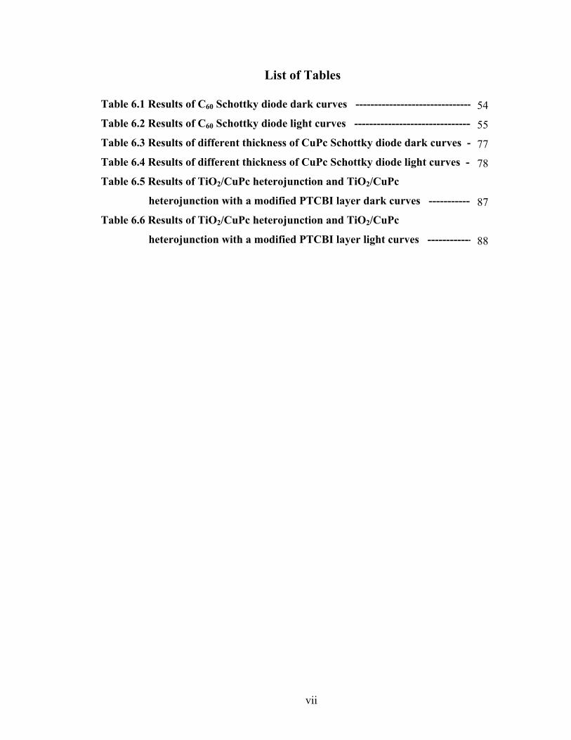
List of Tables Table 6.1 Results of C60 Schottky diode dark curves ----------------------------------
Table 6.2 Results of C60 Schottky diode light curves ---------------------------------- Table 6.3 Results of different thickness of CuPc Schottky diode dark curves -
Table 6.4 Results of different thickness of CuPc Schottky diode light curves -
Table 6.5 Results of TiO2/CuPc heterojunction and TiO2/CuPc
heterojunction with a modified PTCBI layer dark curves -----------
Table 6.6 Results of TiO2/CuPc heterojunction and TiO2/CuPc
heterojunction with a modified PTCBI layer light curves ------------
54
55
77
78
87
88
viii
List of Figures
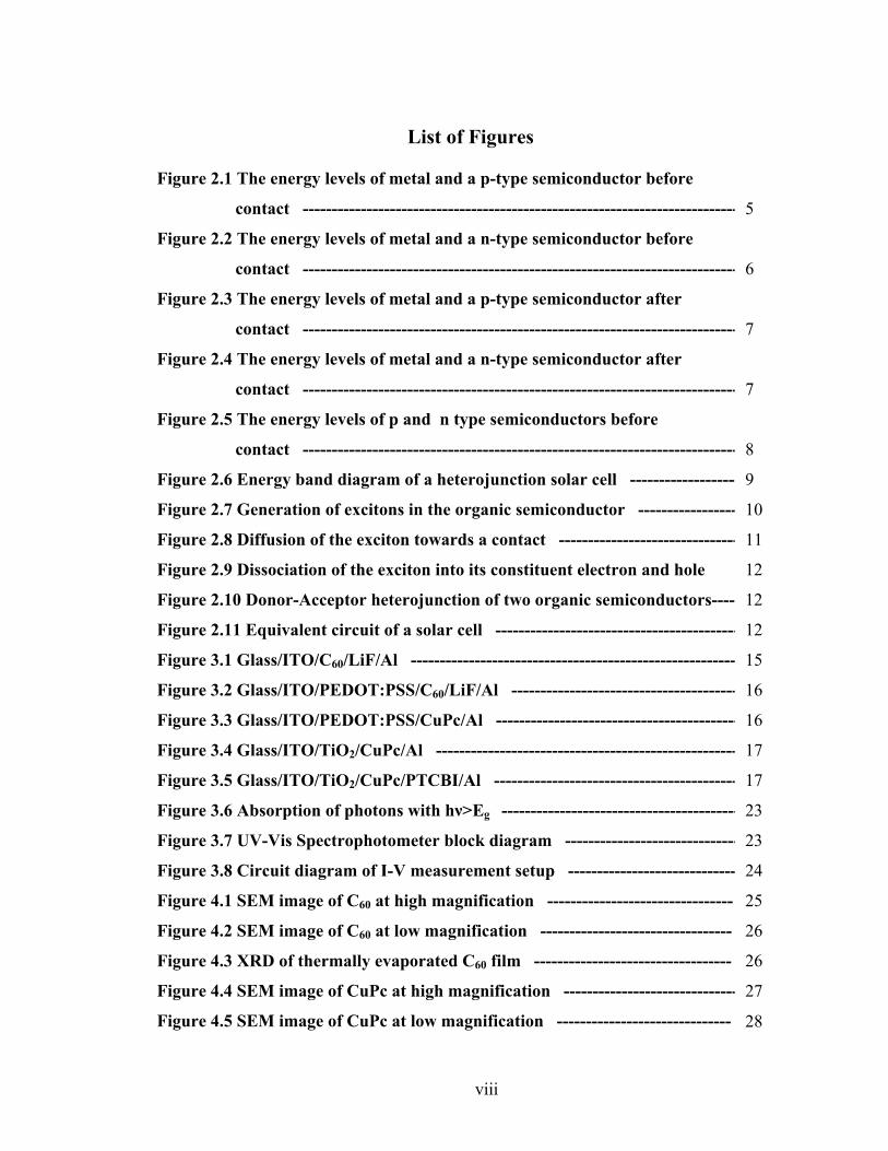
Figure 2.1 The energy levels of metal and a p-type semiconductor before
contact -------------------------------------------------------------------------------
Figure 2.2 The energy levels of metal and a n-type semiconductor before
contact ------------------------------------------------------------------------------
Figure 2.3 The energy levels of metal and a p-type semiconductor after
contact ----------------------------------------------------------------------------
Figure 2.4 The energy levels of metal and a n-type semiconductor after
contact ----------------------------------------------------------------------------
Figure 2.5 The energy levels of p and n type semiconductors before
contact ----------------------------------------------------------------------------
Figure 2.6 Energy band diagram of a heterojunction solar cell -------------------
Figure 2.7 Generation of excitons in the organic semiconductor -------------------
Figure 2.8 Diffusion of the exciton towards a contact ---------------------------------
Figure 2.9 Dissociation of the exciton into its constituent electron and hole
Figure 2.10 Donor-Acceptor heterojunction of two organic semiconductors------------
Figure 2.11 Equivalent circuit of a solar cell -------------------------------------------
Figure 3.1 Glass/ITO/C60/LiF/Al ---------------------------------------------------------
Figure 3.2 Glass/ITO/PEDOT:PSS/C60/LiF/Al ----------------------------------------
Figure 3.3 Glass/ITO/PEDOT:PSS/CuPc/Al -------------------------------------------
Figure 3.4 Glass/ITO/TiO2/CuPc/Al ----------------------------------------------------
Figure 3.5 Glass/ITO/TiO2/CuPc/PTCBI/Al -------------------------------------------
Figure 3.6 Absorption of photons with hν>Eg ------------------------------------------
Figure 3.7 UV-Vis Spectrophotometer block diagram ------------------------------
Figure 3.8 Circuit diagram of I-V measurement setup ------------------------------
Figure 4.1 SEM image of C60 at high magnification --------------------------------
Figure 4.2 SEM image of C60 at low magnification ---------------------------------
Figure 4.3 XRD of thermally evaporated C60 film ----------------------------------
Figure 4.4 SEM image of CuPc at high magnification ------------------------------
Figure 4.5 SEM image of CuPc at low magnification ------------------------------
5
6
7
7
8
9
10
11
12
12
12
15
16
16
17
17
23
23
24
25
26
26
27
28
ix
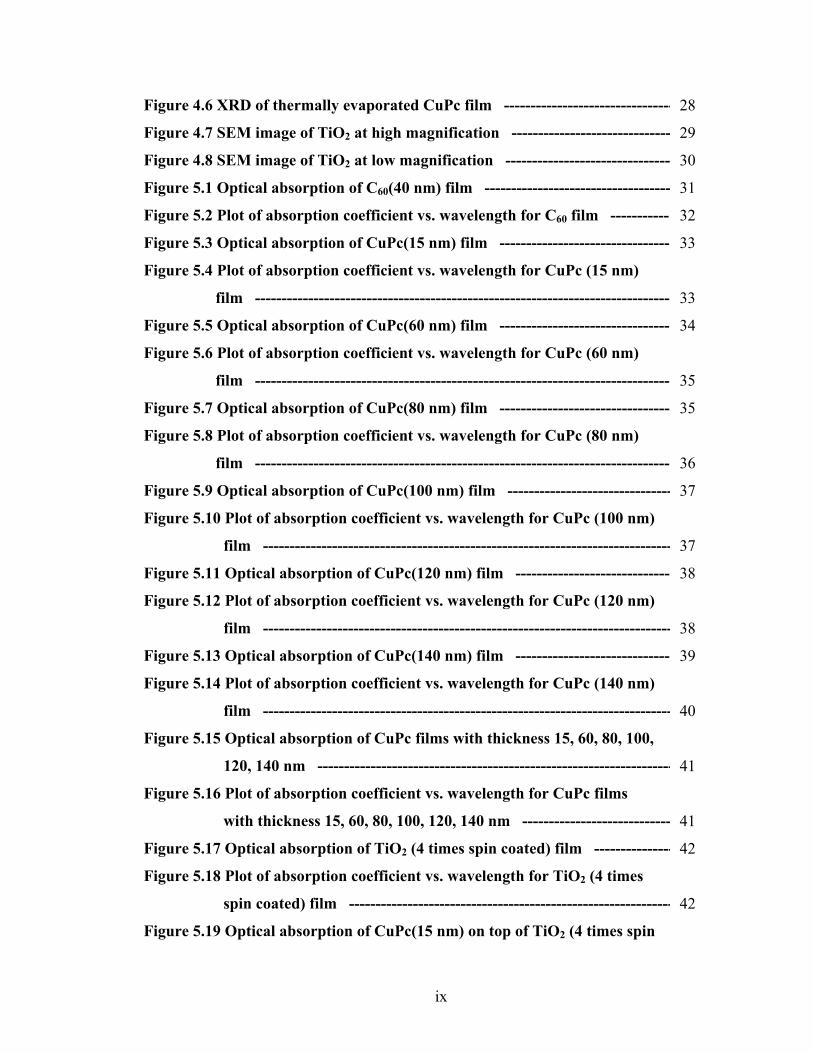
Figure 4.6 XRD of thermally evaporated CuPc film ---------------------------------
Figure 4.7 SEM image of TiO2 at high magnification --------------------------------
Figure 4.8 SEM image of TiO2 at low magnification -------------------------------
Figure 5.1 Optical absorption of C60(40 nm) film -----------------------------------
Figure 5.2 Plot of absorption coefficient vs. wavelength for C60 film -----------
Figure 5.3 Optical absorption of CuPc(15 nm) film --------------------------------
Figure 5.4 Plot of absorption coefficient vs. wavelength for CuPc (15 nm)
film --------------------------------------------------------------------------------
Figure 5.5 Optical absorption of CuPc(60 nm) film --------------------------------
Figure 5.6 Plot of absorption coefficient vs. wavelength for CuPc (60 nm)
film ------------------------------------------------------------------------------
Figure 5.7 Optical absorption of CuPc(80 nm) film --------------------------------
Figure 5.8 Plot of absorption coefficient vs. wavelength for CuPc (80 nm)
film ------------------------------------------------------------------------------
Figure 5.9 Optical absorption of CuPc(100 nm) film -------------------------------
Figure 5.10 Plot of absorption coefficient vs. wavelength for CuPc (100 nm)
film -----------------------------------------------------------------------------
Figure 5.11 Optical absorption of CuPc(120 nm) film ------------------------------
Figure 5.12 Plot of absorption coefficient vs. wavelength for CuPc (120 nm)
film -----------------------------------------------------------------------------
Figure 5.13 Optical absorption of CuPc(140 nm) film ------------------------------
Figure 5.14 Plot of absorption coefficient vs. wavelength for CuPc (140 nm)
film -------------------------------------------------------------------------------
Figure 5.15 Optical absorption of CuPc films with thickness 15, 60, 80, 100,
120, 140 nm --------------------------------------------------------------------
Figure 5.16 Plot of absorption coefficient vs. wavelength for CuPc films
with thickness 15, 60, 80, 100, 120, 140 nm ------------------------------
Figure 5.17 Optical absorption of TiO2 (4 times spin coated) film ---------------
Figure 5.18 Plot of absorption coefficient vs. wavelength for TiO2 (4 times
spin coated) film -------------------------------------------------------------
Figure 5.19 Optical absorption of CuPc(15 nm) on top of TiO2 (4 times spin
28
29
30
31
32
33
33
34
35
35
36
37
37
38
38
39
40
41
41
42
42
x
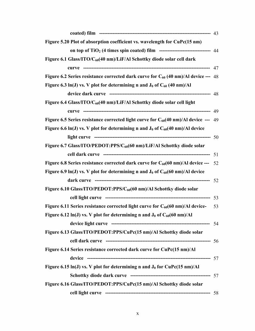
coated) film -------------------------------------------------------------------
Figure 5.20 Plot of absorption coefficient vs. wavelength for CuPc(15 nm)
on top of TiO2 (4 times spin coated) film -------------------------------
Figure 6.1 Glass/ITO/C60(40 nm)/LiF/Al Schottky diode solar cell dark
curve ----------------------------------------------------------------------------
Figure 6.2 Series resistance corrected dark curve for C60 (40 nm)/Al device ----
Figure 6.3 ln(J) vs. V plot for determining n and J0 of C60 (40 nm)/Al
device dark curve --------------------------------------------------------------
Figure 6.4 Glass/ITO/C60(40 nm)/LiF/Al Schottky diode solar cell light
curve -----------------------------------------------------------------------------
Figure 6.5 Series resistance corrected light curve for C60(40 nm)/Al device ---
Figure 6.6 ln(J) vs. V plot for determining n and J0 of C60(40 nm)/Al device
light curve ----------------------------------------------------------------------
Figure 6.7 Glass/ITO/PEDOT:PPS/C60(60 nm)/LiF/Al Schottky diode solar
cell dark curve ----------------------------------------------------------------
Figure 6.8 Series resistance corrected dark curve for C60(60 nm)/Al device ---
Figure 6.9 ln(J) vs. V plot for determining n and J0 of C60(60 nm)/Al device
dark curve ---------------------------------------------------------------------
Figure 6.10 Glass/ITO/PEDOT:PPS/C60(60 nm)/Al Schottky diode solar
cell light curve ---------------------------------------------------------------
Figure 6.11 Series resistance corrected light curve for C60(60 nm)/Al device-
Figure 6.12 ln(J) vs. V plot for determining n and J0 of C60(60 nm)/Al
device light curve -----------------------------------------------------------
Figure 6.13 Glass/ITO/PEDOT:PPS/CuPc(15 nm)/Al Schottky diode solar
cell dark curve ---------------------------------------------------------------
Figure 6.14 Series resistance corrected dark curve for CuPc(15 nm)/Al
device --------------------------------------------------------------------------
Figure 6.15 ln(J) vs. V plot for determining n and J0 for CuPc(15 nm)/Al
Schottky diode dark curve --------------------------------------------------
Figure 6.16 Glass/ITO/PEDOT:PPS/CuPc(15 nm)/Al Schottky diode solar
cell light curve ---------------------------------------------------------------
43
44
47
48
48
49
49
50
51
52
52
53
53
54
56
57
57
58
xi
Figure 6.17 Series resistance corrected light curve for CuPc(15 nm)/Al
device --------------------------------------------------------------------------
Figure 6.18 ln(J) vs. V plot for determining n and J0 for CuPc(15 nm)/Al
Schottky diode light curve -------------------------------------------------
Figure 6.19 Glass/ITO/PEDOT:PPS/CuPc(60 nm)/Al Schottky diode solar
cell dark curve ----------------------------------------------------------------
Figure 6.20 Series resistance corrected dark curve for CuPc(60 nm)/Al
device --------------------------------------------------------------------------
Figure 6.21 ln(J) vs. V plot for determining n and J0 for CuPc(60nm)/Al
Schottky diode dark curve -------------------------------------------------
Figure 6.22 Glass/ITO/PEDOT:PPS/CuPc(60 nm)/Al Schottky diode solar
cell light curve ---------------------------------------------------------------
Figure 6.23 Series resistance corrected light curve for CuPc(60 nm)/Al
device --------------------------------------------------------------------------
Figure 6.24 ln(J) vs. V plot for determining n and J0 for CuPc(60 nm)/Al
Schottky diode light curve -------------------------------------------------
Figure 6.25 Glass/ITO/PEDOT:PPS/CuPc(80 nm)/Al Schottky diode solar
cell dark curve ---------------------------------------------------------------
Figure 6.26 Series resistance corrected dark curve for CuPc(80 nm)/Al
device ---------------------------------------------------------------------------
Figure 6.27 ln(J) vs. V plot for determining n and J0 for CuPc(80 nm)/Al
Schottky diode dark curve -------------------------------------------------
Figure 6.28 Glass/ITO/PEDOT:PPS/CuPc(80 nm)/Al Schottky diode solar
cell light curve ---------------------------------------------------------------
Figure 6.29 Series resistance corrected light curve for CuPc(80 nm)/Al
device -----------------------------------------------------------------------
Figure 6.30 ln(J) vs. V plot for determining n and J0 for CuPc(80 nm)/Al
Schottky diode light curve --------------------------------------------------
Figure 6.31 Glass/ITO/PEDOT:PPS/CuPc(100 nm)/Al Schottky diode solar
cell dark curve ---------------------------------------------------------------
Figure 6.32 Series resistance corrected dark curve for CuPc(100 nm)/Al
58
59
60
60
61
61
62
62
63
63
64
64
65
65
66
xii
device ---------------------------------------------------------------------------
Figure 6.33 ln(J) vs. V plot for determining n and J0 for CuPc(100 nm)/Al
Schottky diode dark curve -------------------------------------------------
Figure 6.34 Glass/ITO/PEDOT:PPS/CuPc(100 nm)/Al Schottky diode solar
cell light curve ---------------------------------------------------------------
Figure 6.35 Series resistance corrected light curve for CuPc(100 nm)/Al
device ---------------------------------------------------------------------------
Figure 6.36 ln(J) vs. V plot for determining n and J0 for CuPc(100 nm)/Al
Schottky diode light curve --------------------------------------------------
Figure 6.37 Glass/ITO/PEDOT:PPS/CuPc(120 nm)/Al Schottky diode solar
cell dark curve ----------------------------------------------------------------
Figure 6.38 Series resistance corrected dark curve for CuPc(120 nm)/Al
device -----------------------------------------------------------------------------
Figure 6.39 ln(J) vs. V plot for determining n and J0 for CuPc(120 nm)/Al
Schottky diode dark curve -------------------------------------------------
Figure 6.40 Glass/ITO/PEDOT:PPS/CuPc(120 nm)/Al Schottky diode solar
cell light curve ----------------------------------------------------------------
Figure 6.41 Series resistance corrected light curve for CuPc(120 nm)/Al
device --------------------------------------------------------------------------
Figure 6.42 ln(J) vs. V plot for determining n and J0 for CuPc(120 nm)/Al
Schottky diode light curve -------------------------------------------------
Figure 6.43 Glass/ITO/PEDOT:PPS/CuPc(140 nm)/Al Schottky diode solar
cell dark curve ----------------------------------------------------------------
Figure 6.44 Series resistance corrected dark curve for CuPc(140 nm)/Al
device ---------------------------------------------------------------------------
Figure 6.45 ln(J) vs. V plot for determining n and J0 for CuPc(140 nm)/Al
Schottky diode dark curve -------------------------------------------------
Figure 6.46 Glass/ITO/PEDOT:PPS/CuPc(140 nm)/Al Schottky diode solar
cell light curve ---------------------------------------------------------------
Figure 6.47 Series resistance corrected light curve for CuPc(140 nm)/Al
device ---------------------------------------------------------------------------
66
67
68
68
69
70
70
71
72
72
73
74
74
75
76
76
xiii
Figure 6.48 ln(J) vs. V plot for determining n and J0 for CuPc(140 nm)/Al
Schottky diode light curve -------------------------------------------------
Figure 6.49 Plot showing the variation of open circuit voltage(Voc) and short
circuit current(Jsc) with thickness of CuPc films ---------------------
Figure 6.50 Glass/ITO/TiO2/CuPc(15 nm)/Al heterojunction solar cell dark
curve ---------------------------------------------------------------------------
Figure 6.51 Series resistance corrected dark curve for
Glass/ITO/TiO2/CuPc(15 nm)/Al device --------------------------------
Figure 6.52 ln(J) vs. V plot for determining n and J0 for
Glass/ITO/TiO2/CuPc(15 nm)/Al device dark curve ------------------
Figure 6.53 Glass/ITO/TiO2/CuPc(15 nm)/Al heterojunction solar cell light
curve ---------------------------------------------------------------------------
Figure 6.54 Series resistance corrected light curve for
Glass/ITO/TiO2/CuPc(15 nm)/Al device --------------------------------
Figure 6.55 ln(J) vs. V plot for determining n and J0 for
Glass/ITO/TiO2/CuPc(15 nm)/Al device light curve ------------------
Figure 6.56 Glass/ITO/TiO2/CuPc(15 nm)/PTCBI(7 nm)Al heterojunction
solar cell dark curve ---------------------------------------------------------
Figure 6.57 Series resistance corrected dark curve for
Glass/ITO/TiO2/CuPc(15 nm)/PTCBI/Al device ----------------------
Figure 6.58 ln(J) vs. V plot for determining n and J0 for
Glass/ITO/TiO2/CuPc(15 nm)/PTCBI/Al device dark curve -------
Figure 6.59 Glass/ITO/TiO2/CuPc(15 nm)/PTCBI(7 nm)Al heterojunction
solar cell light curve ---------------------------------------------------------
Figure 6.60 Series resistance corrected light curve for
Glass/ITO/TiO2/CuPc(15 nm)/PTCBI(7 nm)/Al device --------------
Figure 6.61 ln(J) vs. V plot for determining n and J0 for light curve of
Glass/ITO/TiO2/CuPc(15 nm)/PTCBI(7 nm)/Al device -------------
77
79
80
81
81
82
82
83
84
84
85
86
86
87
xiv
List of Files Thesis-Subhash.pdf ------------------------------------------------------------------ 1.93 MB
1
Chapter 1. Introduction 1.1 Purpose For many years, single crystal devices and thin film devices made of inorganic
materials served as solar cells for industrial and household applications. However, the
trend in recent years has been to use devices whose manufacturing cost is less and which
would provide decent performance. This recent trend urged many of the researchers to
focus on the cheaper alternative to the inorganic materials i.e., the organic solar cells. The
purpose of this research is to gain insight into the different kinds of organic solar cells
i.e., the homojunction, heterojunction and the dispersed heterojunction solar cells. For
this purpose CuPc (acceptor type) and C60 (donor type) were chosen as the basic materials
with which the devices were fabricated.
1.2 A brief history of solar cells In 1839 a French physicist named Antonie-Cesar Becquerel observed that shining
light on an electrode submerged in a conductive solution would create an electric current.
During the same time a physicist named Edmond Becquerel found that certain material
would produce a small amount of electric current when it was exposed to light. This was
described as the photovoltaic (PV) effect. Researchers from various parts of the world
observed this phenomenon and were trying to find a way in which this phenomenon
could be used to generate electricity on a large scale. They found that selenium PV cells
were converting light to electricity. These selenium solar cells had an efficiency of 1% to
2%.
In 1941, an American scientist named Russel Ohl invented a silicon solar cell. In
1954, scientists at Bell Laboratories used the Czochralski process to develop the first
crystalline silicon photovoltaic cell which had an efficiency of 4%. In the second half of
the 20th century the science behind the solar energy was fully understood which led to
improvements in the PV conversion efficiencies.
Solar cells became a good source of electricity for satellites and were also used as
cheaper alternatives for power lines in remote areas. Even today, space use remains the
2
primary application of solar cells. Solar cells could not replace the conventional means
of generating electricity because of the large costs involved in manufacturing them.
1.3 Current trends with solar cells With the accelerated interest in solar cells people searched for more materials which
exhibited photovoltaic properties with higher efficiencies and lower cost of
manufacturing. In the 1960’s scientists turned towards the thin film materials due to their
low cost of production. The thin film solar cells have reduced the cost of production of
solar cells by a considerable amount. Thin film solar cells eliminate the expensive crystal
growth techniques by using closed space sublimation, sputtering and deposition
techniques. However thin film solar cells face some problems such as low efficiency and
short lifetime [1]. In recent years researchers started focusing on cheaper alternatives for
manufacturing solar cells. This paved the way for the organic materials to enter the field
of photovoltaics. The first ever organic solar cell fabricated in the year 1986 [2] had an
efficiency of 1%. Since then the efficiency of the organic solar cells started to increase
and as of now, stands at about 4-5%. The efficiencies of organic solar cells are much less
when compared to their inorganic counterparts but the ease with which they can be
fabricated and also their cost of production makes them a good alternative [3]. Organic
solar cells could be manufactured by printing or spraying the materials on to a roll of
plastic. We could even have a sheet of solar cells that could be unrolled and put on a
roof. The cells also could be made in different colours or even be transparent making
them good architectural elements.
Organic solar cells are plagued with problems such as low efficiency and shorter
lifetime. Today most of the research is focused on improving the efficiency and also to
increase the lifetime of these cells.
1.4 C60 based Schottky diode solar cells C60 also known as buckminster fullerene is a spherical shaped molecule which is
used as an n-type organic semiconductor. C60 Schottky diode solar cells with
ITO(Indium Tin Oxide)/C60/Al structure and efficiencies of less than 104 were reported
by Tetsuya Taima et al., [4]. They reported an open circuit voltage of 0.046 V and a
3
short circuit current of 2.77 x 10² mA/cm2. In this thesis, an effort has been made to
increase the efficiency of these solar cells by improving the open circuit voltage and short
circuit current. PEDOT:PSS(3, 4-polyethylenedioxythiophene: polystyrene sulfonate)
was spincoated onto the ITO coated glass before the deposition of C60 to make the surface
of ITO smooth. Also, LiF was deposited on the C60 film before the deposition of
aluminium contacts to protect the surface of C60 from high energy Al atoms. The devices
are characterized by SEM (Scanning Electron Microscopy), UV-Vis (Ultra Violet-Visible
spectroscopy), XRD (X-Ray Diffraction) and I-V (Current-Voltage) measurements.
1.5 CuPc based Schottky diode solar cells
CuPc stands for Copper Phthalocyanine a p-type organic semiconductor which is
widely used because of its low cost and good photoelectronic properties [5-6]. CuPc
Schottky diode solar cells with ITO/CuPc (100 nm)/Al structure were fabricated by C.W.
Kwong et al., [7] and they have reported a open circuit voltage of 0.94 V, short circuit
current density of 23.5 µA/cm2 and an efficiency of 0.00406 %. Organic Schottky diode
solar cells are less efficient when compared to their inorganic counterparts because of
low carrier mobility. In this thesis, we tried to study the effect of varying the thickness of
the CuPc layer on the cell parameters such as open circuit voltage, short circuit current
and efficiency etc.. As in the case of the C60 Schottky diode solar cells, PEDOT:PSS was
spincoated on the surface of ITO coated glass before the deposition of CuPc to smooth
out the irregularities of the ITO surface. Also the devices were characterized by SEM,
UV-Vis, XRD and I-V measurements.
1.6 TiO2/CuPc/Al and TiO2/CuPc/PTCBI/Al solar cells Titanium dioxide (TiO2) is a well known n-type semiconductor. TiO2/CuPc
heterojunctions with structure ITO/TiO2/CuPc (460 nm)/Au were fabricated by A. K. Ray
et al., [8] with an open circuit voltage of 0.024 V, 0.012 mA/cm2 at an illumination of 60
mW/cm2. Annealed spin coated titanium dioxide films are known to produce porous
films which can be used for the scattering of light, and thereby increasing the effective
optical path of light. In this thesis, an attempt has been made to reduce the thickness of
the CuPc film to avoid the recombination of the carriers, and thus to produce better
4
efficiency. UV-Vis measurements were made to check the peaks of the absorption
curves. Also, SEM and I-V measurements were made to calculate the cell parameters.
5
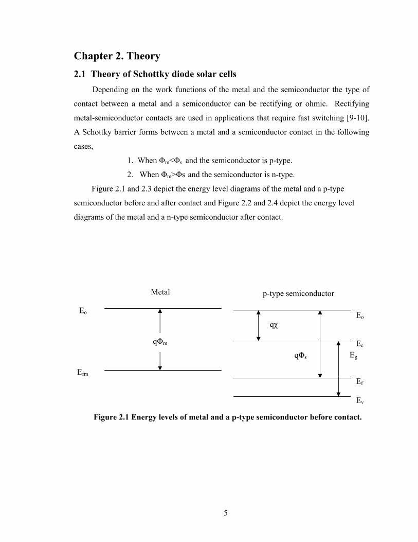
Chapter 2. Theory
2.1 Theory of Schottky diode solar cells Depending on the work functions of the metal and the semiconductor the type of
contact between a metal and a semiconductor can be rectifying or ohmic. Rectifying
metal-semiconductor contacts are used in applications that require fast switching [9-10].
A Schottky barrier forms between a metal and a semiconductor contact in the following
cases,
1. When Φm<Φs and the semiconductor is p-type.
2. When Φm>Φs and the semiconductor is n-type.
Figure 2.1 and 2.3 depict the energy level diagrams of the metal and a p-type
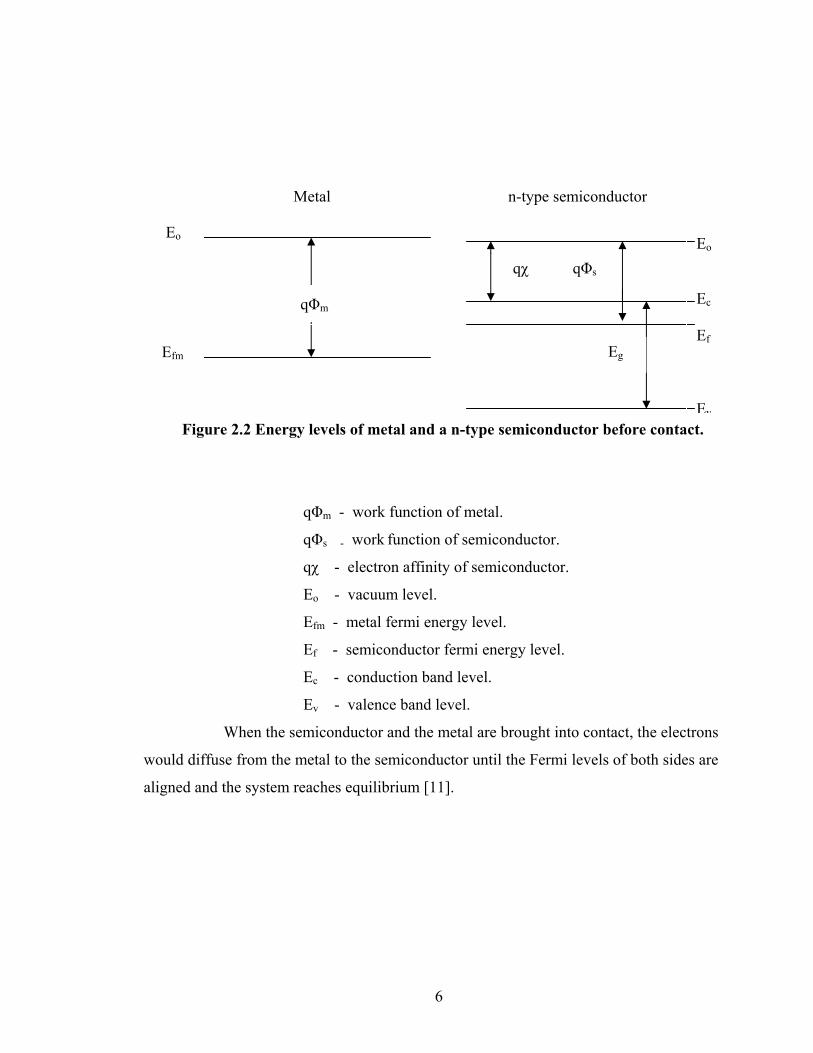
semiconductor before and after contact and Figure 2.2 and 2.4 depict the energy level
diagrams of the metal and a n-type semiconductor after contact.
Figure 2.1 Energy levels of metal and a p-type semiconductor before contact.
qΦm
Eo
Efm
Metal
Eo Ec Ef Ev
qΦs
qχ
p-type semiconductor
Eg
6
Figure 2.2 Energy levels of metal and a n-type semiconductor before contact.
qΦm - work function of metal.
qΦs - work function of semiconductor.
qχ - electron affinity of semiconductor.
Eo - vacuum level.
Efm - metal fermi energy level.
Ef - semiconductor fermi energy level.
Ec - conduction band level.
Ev - valence band level.
When the semiconductor and the metal are brought into contact, the electrons
would diffuse from the metal to the semiconductor until the Fermi levels of both sides are
aligned and the system reaches equilibrium [11].
Metal n-type semiconductor
qΦm
qχ qΦs
Eo
Efm
Eo Ec Ef Ev
Eg
7
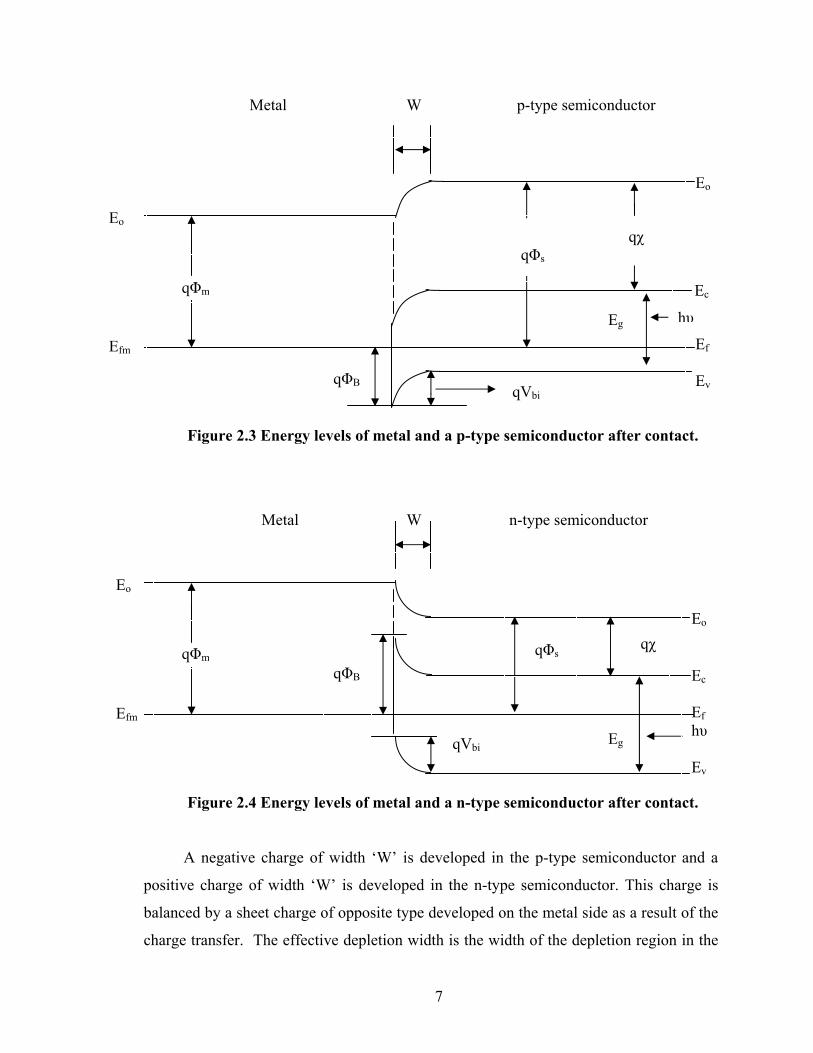
Figure 2.3 Energy levels of metal and a p-type semiconductor after contact.
Figure 2.4 Energy levels of metal and a n-type semiconductor after contact. A negative charge of width ‘W’ is developed in the p-type semiconductor and a
positive charge of width ‘W’ is developed in the n-type semiconductor. This charge is
balanced by a sheet charge of opposite type developed on the metal side as a result of the
charge transfer. The effective depletion width is the width of the depletion region in the
qΦm
Eo Efm
Metal W n-type semiconductor
qΦB
Ef Ev
Ef hυ Ev
qΦs
qχ
Ec
Eo
qΦs qχ
qΦB
qVbi
hυ
qVbi
Eo Efm
qΦm
Metal W p-type semiconductor
Eg
Eg
Ec
Eo

8
semiconductor, as the width of the sheet charge in the metal is negligible. Light with
energy greater than ‘Eg’ will be absorbed by the n-type and the p-type material, and the
carriers created in the depletion region and within a diffusion length of the junction will
be collected. The separation of the light generated carriers across the barrier gives rise to
the light generated current IL.
2.2 Theory of Heterojunction Solar Cells A heterojunction is formed between two semiconductors with different crystal
structure, bandgap and other properties. Consider separate n-type and p-type
semiconductor crystals. The energy band diagram for the n and p type semiconductors
before contact is shown in Figure 2.5. The difference in electron concentrations between
the two materials causes electrons to flow from n to p-type semiconductor and holes from
p to n-type semiconductor when the two materials are brought together. This movement
of the carriers into the oppositely doped materials leads to a charge build up near the
junction and a subsequent electric field. This electric field extends from the n-side of the
junction to the p-side. The energy band diagram of the p-type and the n-type
semiconductors after the contact is depicted in Figure 2.6.
Figure 2.5 Energy levels of p and n type semiconductors before contact.
Eo
Ec Ef Ev
Eo
Ec Ef Ev
p-type n-type
Eg1 Eg2
qχp qχn qΦp qΦn
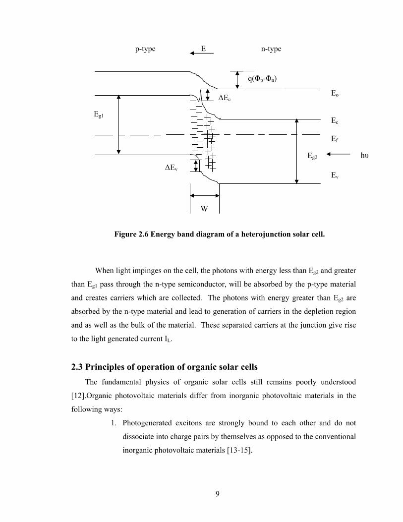
9
Figure 2.6 Energy band diagram of a heterojunction solar cell.
When light impinges on the cell, the photons with energy less than Eg2 and greater
than Eg1 pass through the n-type semiconductor, will be absorbed by the p-type material
and creates carriers which are collected. The photons with energy greater than Eg2 are
absorbed by the n-type material and lead to generation of carriers in the depletion region
and as well as the bulk of the material. These separated carriers at the junction give rise
to the light generated current IL.
2.3 Principles of operation of organic solar cells The fundamental physics of organic solar cells still remains poorly understood
[12].Organic photovoltaic materials differ from inorganic photovoltaic materials in the
following ways:
1. Photogenerated excitons are strongly bound to each other and do not
dissociate into charge pairs by themselves as opposed to the conventional
inorganic photovoltaic materials [13-15].
Eo
Ec Ef Ev
p-type E n-type
W
q(Φp-Φn)
Eg1
Eg2 hυ ∆Ev
∆Ec
10
2. The mobilities of these charges are less when compared to those of
inorganic materials.
3. The spectral range of absorption is relatively narrow when compared to
the inorganic materials.
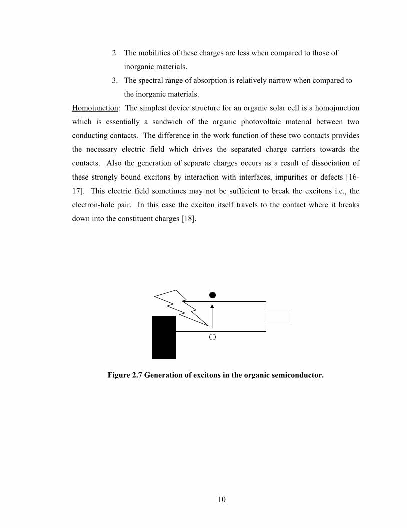
Homojunction: The simplest device structure for an organic solar cell is a homojunction
which is essentially a sandwich of the organic photovoltaic material between two
conducting contacts. The difference in the work function of these two contacts provides
the necessary electric field which drives the separated charge carriers towards the
contacts. Also the generation of separate charges occurs as a result of dissociation of
these strongly bound excitons by interaction with interfaces, impurities or defects [16-
17]. This electric field sometimes may not be sufficient to break the excitons i.e., the
electron-hole pair. In this case the exciton itself travels to the contact where it breaks
down into the constituent charges [18].
Figure 2.7 Generation of excitons in the organic semiconductor.
11
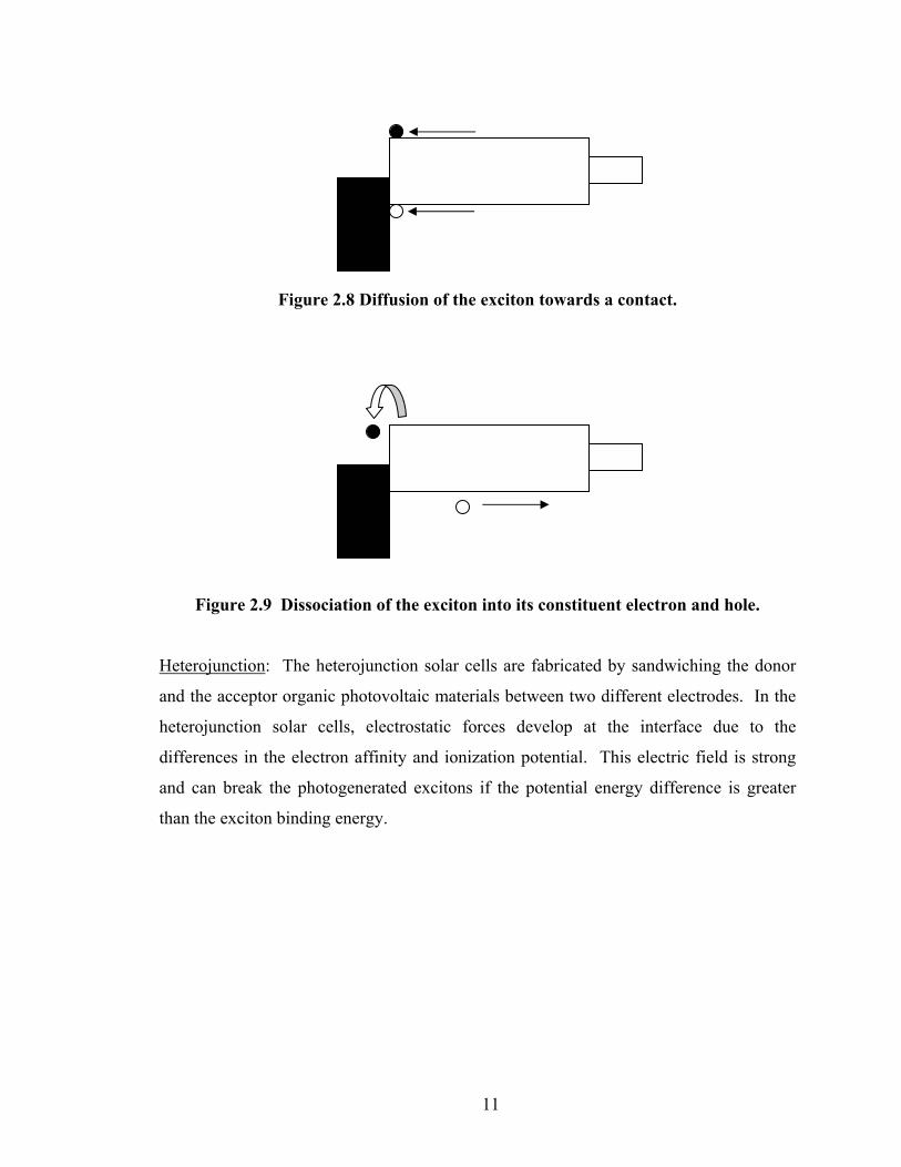
Figure 2.8 Diffusion of the exciton towards a contact.
Figure 2.9 Dissociation of the exciton into its constituent electron and hole.
Heterojunction: The heterojunction solar cells are fabricated by sandwiching the donor
and the acceptor organic photovoltaic materials between two different electrodes. In the
heterojunction solar cells, electrostatic forces develop at the interface due to the
differences in the electron affinity and ionization potential. This electric field is strong
and can break the photogenerated excitons if the potential energy difference is greater
than the exciton binding energy.
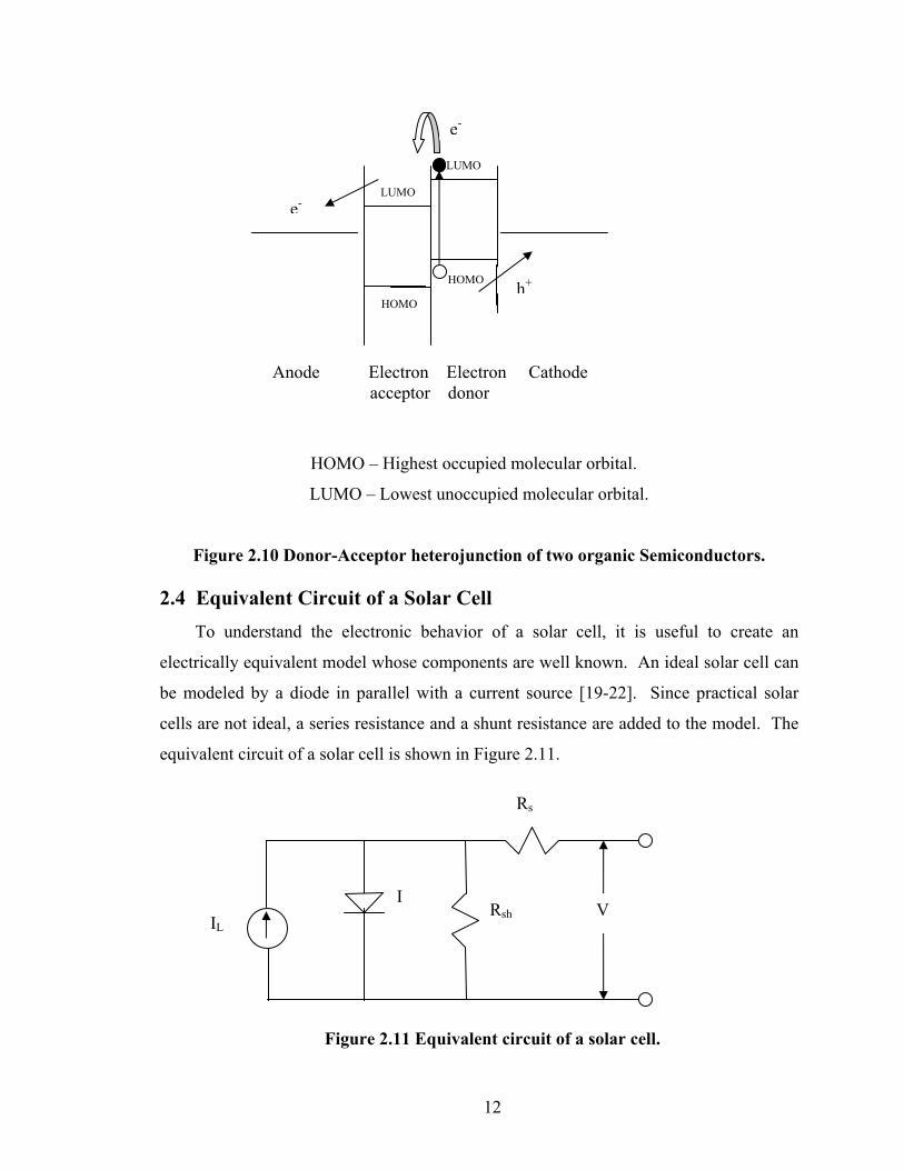
12
HOMO – Highest occupied molecular orbital.
LUMO – Lowest unoccupied molecular orbital.
Figure 2.10 Donor-Acceptor heterojunction of two organic Semiconductors.
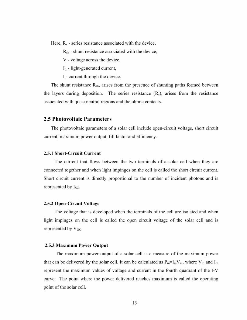
2.4 Equivalent Circuit of a Solar Cell
To understand the electronic behavior of a solar cell, it is useful to create an
electrically equivalent model whose components are well known. An ideal solar cell can
be modeled by a diode in parallel with a current source [19-22]. Since practical solar
cells are not ideal, a series resistance and a shunt resistance are added to the model. The
equivalent circuit of a solar cell is shown in Figure 2.11.
Figure 2.11 Equivalent circuit of a solar cell.
IL Rsh
Rs
IV
LUMO
LUMO
HOMO
HOMO
e-
e-
h+
Anode Electron Electron Cathode acceptor donor
13
Here, Rs - series resistance associated with the device,
Rsh - shunt resistance associated with the device,
V - voltage across the device,
IL - light-generated current,
I - current through the device.
The shunt resistance Rsh, arises from the presence of shunting paths formed between
the layers during deposition. The series resistance (Rs), arises from the resistance
associated with quasi neutral regions and the ohmic contacts.
2.5 Photovoltaic Parameters The photovoltaic parameters of a solar cell include open-circuit voltage, short circuit
current, maximum power output, fill factor and efficiency.
2.5.1 Short-Circuit Current
The current that flows between the two terminals of a solar cell when they are
connected together and when light impinges on the cell is called the short circuit current.
Short circuit current is directly proportional to the number of incident photons and is
represented by ISC.
2.5.2 Open-Circuit Voltage
The voltage that is developed when the terminals of the cell are isolated and when
light impinges on the cell is called the open circuit voltage of the solar cell and is
represented by VOC.
2.5.3 Maximum Power Output
The maximum power output of a solar cell is a measure of the maximum power
that can be delivered by the solar cell. It can be calculated as Pm=ImVm, where Vm and Im
represent the maximum values of voltage and current in the fourth quadrant of the I-V
curve. The point where the power delivered reaches maximum is called the operating
point of the solar cell.
14
2.5.4 Fill Factor
The fill factor of a solar cell is defined as the ratio of VmIm and VocIsc and it
describes the squareness of the I-V curve.
Fill Factor = VmIm/VocIsc 2.1
2.5.5 Efficiency
The efficiency of a solar cell is defined as the ratio of the power delivered at the
operating point and the incident power.
η = (VmIm/Pin)x100% 2.2
Efiiciency is related to Isc and Voc using fill factor(FF) as
η = Isc Voc FF/Pin 2.3
15
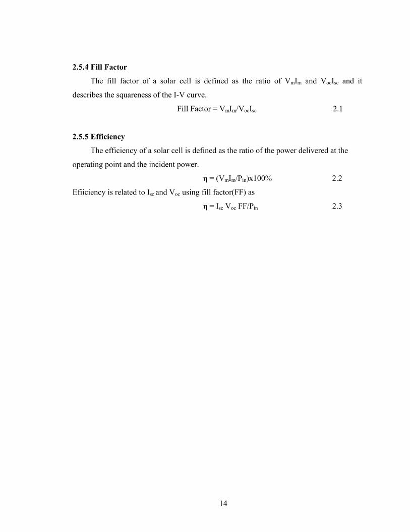
Chapter 3. Experimental 3.1 Device Fabrication 3.1.1 Device Structures
Devices with structure
1) Glass/ITO/C60/LiF/Al
2) Glass/ITO/PEDOT:PSS/C60/LiF/Al
3) Glass/ITO/PEDOT:PSS/CuPc/Al
4) Glass/ITO/TiO2/CuPc/Al
5) Glass/ITO/TiO2/CuPc/PTCBI/Al
were fabricated. Figures 3.1, 3.2, 3.3, 3.4 and 3.5 depict the structure of the solar cells
fabricated. ITO coated glass substrates were commercially purchased from Delta
Technologies, Limited, Stillwater, MN. ITO, a transparent conductor serves as the
bottom contact to the films and the glass provides mechanical support.
Figure 3.1 Glass/ITO/C60/LiF/Al.
GLASS
ITO
C60 LiF
Al
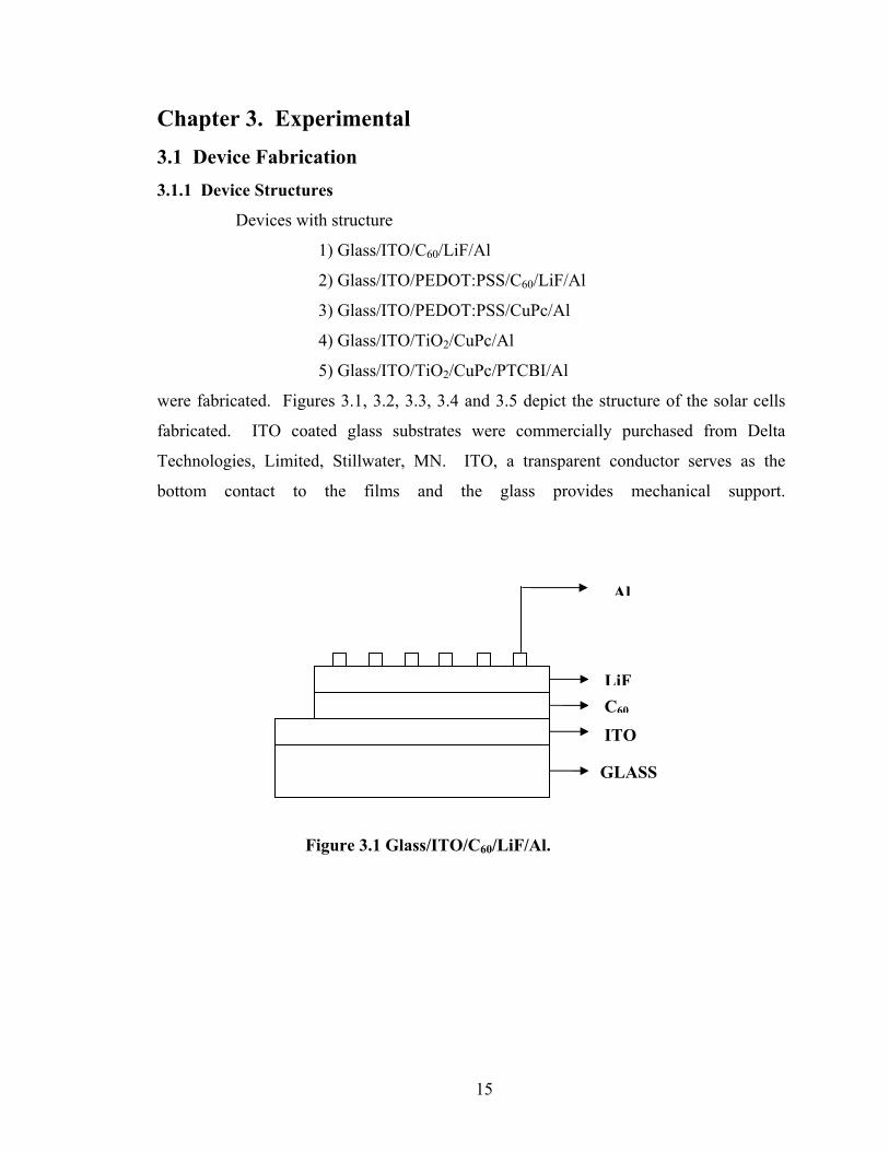
16
Figure 3.2 Glass/ITO/PEDOT:PSS/C60/LiF/Al.
Figure 3.3 Glass/ITO/PEDOT:PSS/CuPc/Al.
GLASS
ITO
PEDOT:PSSC60
Al
LiF
GLASS
ITO
PEDOT:PSSCuPc
Al

17
Figure 3.4 Glass/ITO/TiO2/CuPc/Al.
Figure 3.5 Glass/ITO/TiO2/CuPc/PTCBI/Al.
GLASS
ITO TiO2
CuPc
Al
PTCBI
GLASS
ITO
TiO2 CuPc
Al
18
3.1.2 Preparation of TiO2 Sol-Gel
TiO2 films were prepared by Sol-gel [23-24]. The reagents, namely titanium Tetra
isopropoxide (99.999%), isopropanol (99.5%) and nitric acid (70% redistilled) were
procured from Aldrich. The precursor titanium tetra isopropoxide (TTIP) was dissolved
in isopropanol in a nitrogen environment to which deionized water and then nitric acid
were added. The solution was stored in a nitrogen environment after being stirred for 2
hours. A typical preparation of 0.1 M TiO2 solution contained 1 ml of TTIP, 0.05 ml of
HNO3 (70% distilled), 0.1 ml de-ionized water and 32.7 ml of isopropanol.
3.1.3 Substrate Cleaning
Prior to the fabrication of the devices the ITO coated glass substrates were cleaned
thoroughly. Cleaning the substrates is an essential step which is performed prior to
spincoating the PEDOT:PSS and TiO2 films to obtain smooth and contaminant free films
on the ITO coated glass. Initially the substrates were cleaned with de-ionized water. The
substrates were then transferred to a beaker containing acetone and sonicated for about 10
minutes. The substrates were then cleaned again with de-ionized water. Then, the
substrates were again transferred to a beaker containing methanol and sonicated for 10
minutes. The substrates were then cleaned with de-ionized water and were finally dried
with flowing nitrogen. The ITO coated glass substrates were then electrically
characterized to identify the ITO coated side by applying a small voltage on each side of
the substrate and measuring the resulting current. The side of the glass without the ITO
coating does not allow the passage of any current through it.
3.1.4 Spincoating of the PEDOT:PSS film for device structures 2 and 3
PEDOT:PSS was purchased from Bayer. The PEDOT:PSS films were spincoated
onto the ITO side of the substrates using Chemat technology spin coater. The speed of
the spincoater was set to 4000 rpm and the duration of the spin was 40 seconds. The
substrates were then annealed in a Fisher-Scientific furnace at a temperature of 100oC for
about 1 hour to dry the PEDOT:PSS films and also to increase the adhesion of the films.
19
3.1.5 Spincoating of the TiO2 sol-gel for device structures 4 and 5
TiO2 solution prepared using the sol-gel technique was spin coated on the surface
of the ITO coated glass substrates. The speed of the spincoater was set to 2000 rpm and
the duration of the spin was 40 seconds. The substrates were then annealed overnight in
a Boekel Industries furnace at a temperature of 300oC to increase the adhesion of the
films.
3.1.6 Fabrication of C60 films
The C60 films were made by thermal evaporation of the powdered C60 obtained
from Sigma-Aldrich. The C60 powder was kept in a molybdenum boat and a current of
the order of approximately 4.0 A was passed through the boat. During the evaporation
process, the pressure in the chamber was maintained at 1x10⁻⁶ Torr. The substrates were
attached to a disc at a height of 30cms from the C60 source. The current was increased in
steps of 0.5 A upto 4.0 A. The pressure in the chamber is maintained at the same level all
through the evaporation process to maintain the uniformity of the films. The high
vacuum in the chamber is required to avoid the vapors being deflected and also to avoid
the oxidation of the films. The thickness of the C60 films was monitored using a quartz
crystal monitor. A LiF layer was deposited on the C60 layer to protect it from high energy
Aluminium atoms [25].
3.1.7 Fabrication of CuPc films
The CuPc films were made by thermal evaporation of the powdered CuPc obtained
from Sigma-Aldrich. The powdered CuPc was kept in a molybdenum boat and a
current of approximately 3.7 A was passed through the boat. During the evaporation
process, the pressure in the chamber was maintained at 1x10⁻⁶ Torr. The substrates were
attached to a disc at a height of 30 cms from the CuPc source. The current was increased
in steps of 0.5 A upto 3.7 A. The pressure in the chamber is maintained at the same level
all through the evaporation process to maintain the uniformity of the films. The high
vacuum in the chamber is required to avoid the vapors being deflected and also to avoid
the oxidation of the films. The thickness of the CuPc films was monitored using a quartz
crystal monitor.
20
3.1.8 Fabrication of PTCBI (3,4,9,10-perylenetetracarboxylic bis-benzimidazole)
films
The PTCBI films were made by thermal evaporation of the powdered PTCBI
obtained from Dr. Anthony’s lab in the Chemistry department at the University of
Kentucky. The powdered PTCBI was kept in a molybdenum boat and a current of
approximately 4.2 A was passed through the boat. During the evaporation process the
pressure in the chamber was maintained at 1x10⁻⁶ Torr. The substrates were attached to a
disc at a height of 30cms from the PTCBI source. The current was increased in steps of
0.5 A upto 4.2 A. The pressure in the chamber is maintained at the same level all through
the evaporation process to maintain the uniformity of the films. The high vacuum in the
chamber is required to avoid the vapors being deflected and also to avoid the oxidation of
the films. The thickness of the CuPc films was monitored using a quartz crystal monitor.
3.1.9 Deposition of Aluminium contacts
The aluminium contacts were made on the films by thermal evaporation of
aluminium. We used a tungsten basket for depositing the aluminium electrodes.
Aluminium pellets purchased from Sigma-Aldrich were kept in a tungsten basket and the
chamber was left pumping overnight since the current required for the evaporation of
aluminium electrodes is high, which in turn increases the pressure in the chamber. The
current that was passed through the basket was approximately 4.8 A. The substrates were
covered with a mask of aluminium foil in which circular holes of area 0.07cm2 were
made. The aluminium gets deposited in these circular holes thus creating circular
electrodes of 0.07cm2 area. After the deposition of aluminium the chamber was left to
cool down for about two hours and then the devices were measured for J-V
characteristics.
3.2 X-Ray Diffraction (XRD) In XRD, a diffraction pattern results from the interaction of x-rays with the material.
XRD provides information regarding the phase, structure and composition of the material
[26]. An XRD pattern is unique for each material.
X-rays are diffracted by a series of planes whose orientation is defined with the
Miller indices h, k and l when incident on a crystal. If a, b and c are considered to be
21
axes of the unit cell then h, k and l would cut the axes a, b and c into h, k and l sections
respectively. The constructive interference would occur at an angle of incidence θ which
satisfies Bragg’s law given in equation 3.1.
2dsinθ = nλ 3.1
where d is the spacing between the parallel planes
n is an integer
λ is the wavelength of the x-rays.
The d-spacing among the planes in the crystal corresponds to the peak intensities at
2θ positions obtained from the XRD pattern. By comparing with the previously
calculated reference the indices of the planes and the phase of the material can be
estimated. The material can be identified by comparing with a standard set of data.
3.3 Field Emission Scanning Electron Microscopy (FE-SEM) In Field Emission Scanning Electron Microscopy a beam of electrons generated by a
field emission source scans the surface of the sample. The electrons which are generated
in an electron gun are accelerated in a column with a high electrical field gradient. When
the electrons bombard the sample, back scattered electrons, secondary electrons, light,
heat and transmitted electrons are generated. Backscattered electrons are the ones that
are bounced off the nuclei of atoms in the sample. Secondary electrons are the electrons
from the sample. An electronic signal is generated by a detector which catches the
secondary electrons. From the velocity and angle of the secondary electrons, the surface
structure of the sample can be determined. Finally the signal is processed with amplifiers
and the image is seen on the monitor [27].
3.3.1 Sample Preparation
The samples are mounted on copper stubs specifically available for SEM imaging.
The copper stubs were cleaned by sonicating them with acetone and DI water. Later,
they were wiped clean with kim wipes and dried in flowing nitrogen. A graphite tape of
dimensions 2 mm x 6 mm was cut and pasted on the copper stub. Now the test sample is
cut with dimensions less than the graphite tape and is firmly placed on the graphite tape.
A conducting colloidal graphite paste is used to cover the edges of the sample by using a
22
paint brush. Finally the samples are coated with gold before placing them in the SEM
chamber.
3.3.2 Specimen Exchange
The specimen exchange chamber is isolated from the main chamber so that the air
does not enter the main chamber. The specimen holder in the specimen exchange
chamber has a set of grooves to hold the stub. The specimen is placed in the required
groove depending on the thickness and imaging requirements. By following the standard
procedures the specimen holder is replaced into the specimen exchange chamber.
3.3.3 SEM Imaging
The sample under test is first focused with low magnification. The object is then
moved to the center of the screen and focused with high magnification. The aperture
align switch is turned on and the sample checked for horizontal or vertical swing. In the
presence of a swing the screws on the aperture holder are adjusted until the swing
disappears. The image is then sharpened using the X and Y stigmator controls. This is
done until we obtain the sharpest image.
3.4 Optical Absorption Optical absorption is a technique used to calculate the bandgap energy (Eg) of a
semiconductor. The absorption is recorded by making photons of selected wavelength
incident on the sample under test. A semiconductor consists of a valence band which has
electrons and a conduction band which is empty. When the sample is hit with photons
the electrons absorb photons with energy higher than the bandgap (Eg) and jump to the
conduction band as shown in Figure 3.5. The photons with energy less than the bandgap
(Eg) are not absorbed since they cannot supply the electrons with energy required to cross
the bandgap. The electrons which were initially excited and which have crossed to the
conduction band, loose that excess energy to the lattice and reach thermal equilibrium.
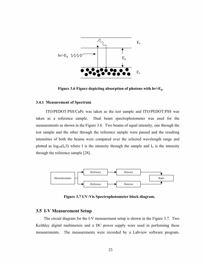
23
Figure 3.6 Figure depicting absorption of photons with hν>Eg.
3.4.1 Measurement of Spectrum ITO/PEDOT:PSS/CuPc was taken as the test sample and ITO/PEDOT:PSS was
taken as a reference sample. Dual beam spectrophotometer was used for the
measurements as shown in the Figure 3.6. Two beams of equal intensity, one through the
test sample and the other through the reference sample were passed and the resulting
intensities of both the beams were compared over the selected wavelength range and
plotted as log10(Io/I) where I is the intensity through the sample and Io is the intensity
through the reference sample [28].
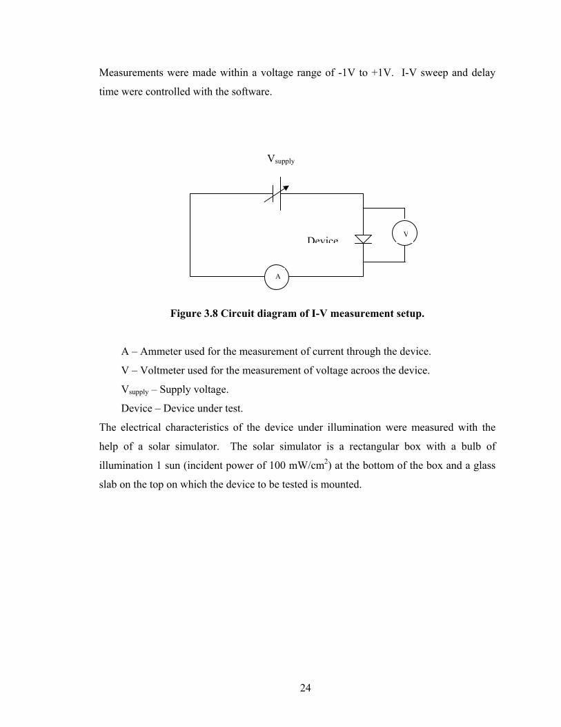
Figure 3.7 UV-Vis Spectrophotometer block diagram. 3.5 I-V Measurement Setup The circuit diagram for the I-V measurement setup is shown in the Figure 3.7. Two
Keithley digital multimeters and a DC power supply were used in performing these
measurements. The measurements were recorded by a Labview software program.
Ev
Ec
Eg hν>Eg
Monochromator
Reference
Reference
Detector
Detector
Ratio
24
Measurements were made within a voltage range of -1V to +1V. I-V sweep and delay
time were controlled with the software.
Figure 3.8 Circuit diagram of I-V measurement setup.
A – Ammeter used for the measurement of current through the device.
V – Voltmeter used for the measurement of voltage acroos the device.
Vsupply – Supply voltage.
Device – Device under test.
The electrical characteristics of the device under illumination were measured with the
help of a solar simulator. The solar simulator is a rectangular box with a bulb of
illumination 1 sun (incident power of 100 mW/cm2) at the bottom of the box and a glass
slab on the top on which the device to be tested is mounted.
V
A
Vsupply
Device
25
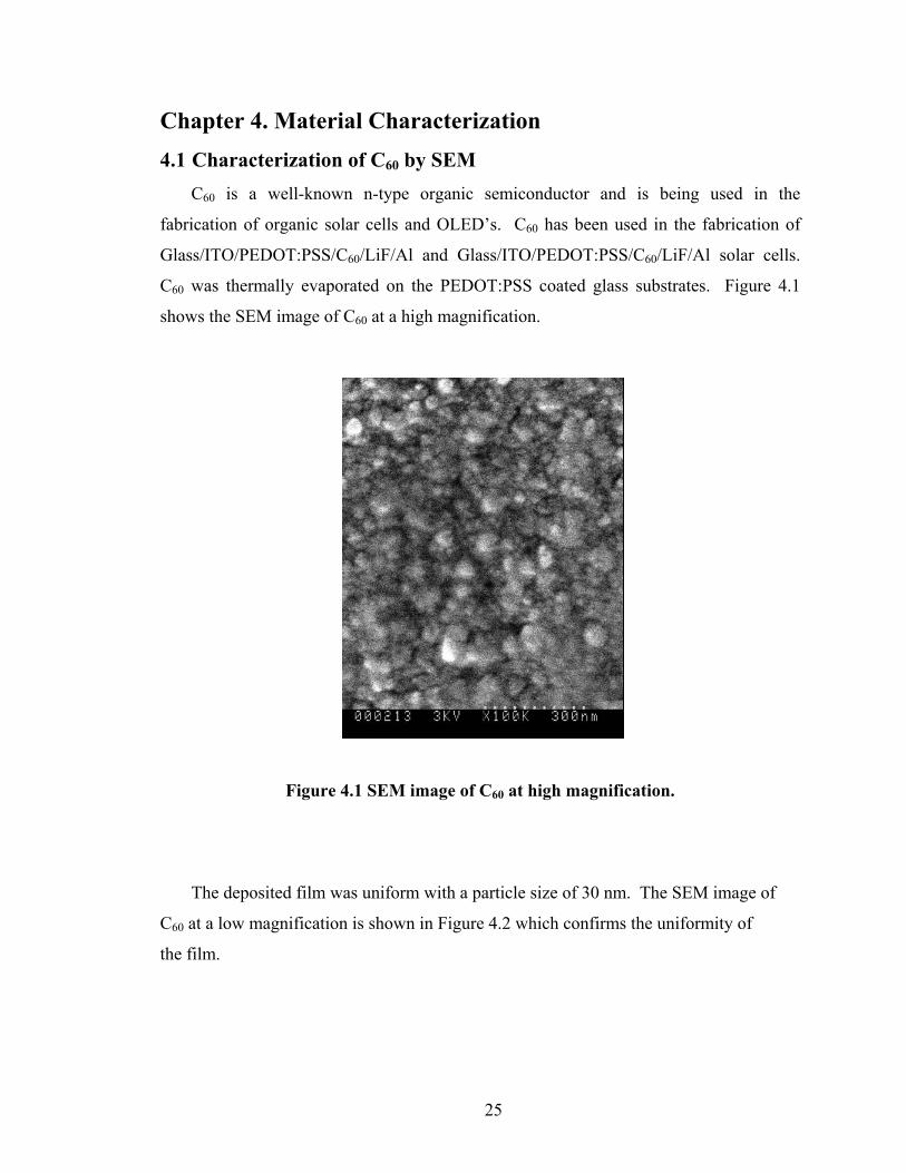
Chapter 4. Material Characterization 4.1 Characterization of C60 by SEM C60 is a well-known n-type organic semiconductor and is being used in the
fabrication of organic solar cells and OLED’s. C60 has been used in the fabrication of
Glass/ITO/PEDOT:PSS/C60/LiF/Al and Glass/ITO/PEDOT:PSS/C60/LiF/Al solar cells.
C60 was thermally evaporated on the PEDOT:PSS coated glass substrates. Figure 4.1
shows the SEM image of C60 at a high magnification.
Figure 4.1 SEM image of C60 at high magnification.
The deposited film was uniform with a particle size of 30 nm. The SEM image of
C60 at a low magnification is shown in Figure 4.2 which confirms the uniformity of
the film.
26
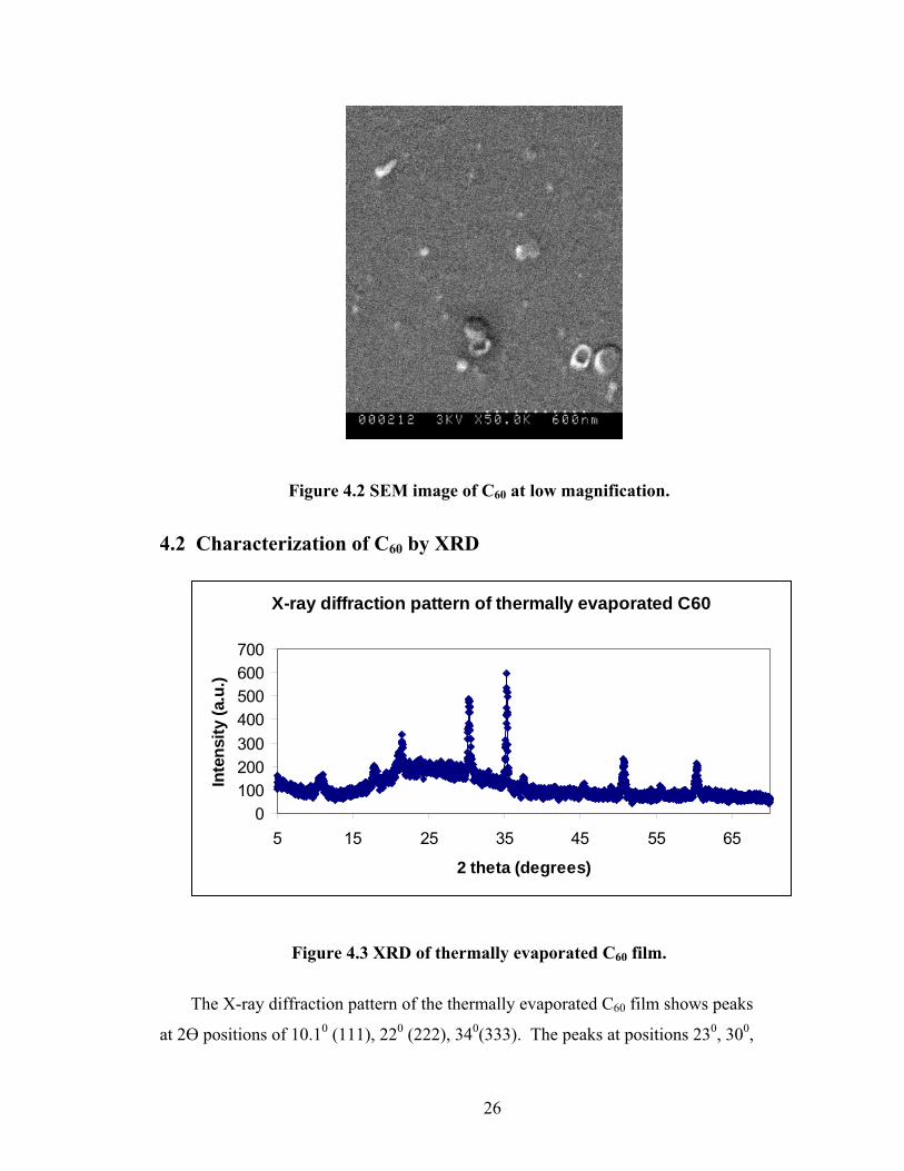
Figure 4.2 SEM image of C60 at low magnification.
4.2 Characterization of C60 by XRD
X-ray diffraction pattern of thermally evaporated C60
0100200300400500600700
5 15 25 35 45 55 65
2 theta (degrees)
Inte
nsity
(a.u
.)
Figure 4.3 XRD of thermally evaporated C60 film.
The X-ray diffraction pattern of the thermally evaporated C60 film shows peaks
at 2Ө positions of 10.10 (111), 220 (222), 340(333). The peaks at positions 230, 300,

27
350, 370, 450, 510 and 600 are produced by ITO.
4.3 Characterization of CuPc by SEM CuPc is a well known p-type organic semiconductor used in the fabrication of
organic solar cells and OLED’s. CuPc was used in the fabrication of devices
Glass/ITO/PEDOT:PSS/CuPc/Al, Glass/ITO/TiO2/CuPc/Al and
Glass/ITO/TiO2/CuPc/PTCBI/Al. Figure 4.4 shows the SEM image of the thermally
evaporated CuPc film on an ITO coated glass substrate at a high magnification.
Figure 4.4 SEM image of CuPc at high magnification.
From Figure 4.4 it can be observed that the average particle size of the thermally
evaporated CuPc film is around 30 nm. Figure 4.5 shows the SEM image of the CuPc
film at a lower magnification. From Figure 4.5 it can be seen that the CuPc film is
uniform.
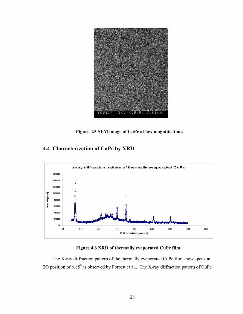
28
Figure 4.5 SEM image of CuPc at low magnification.
4.4 Characterization of CuPc by XRD
x-ray diffraction pattern of thermally evaporated CuPc
0
200
400
600
800
1000
1200
1400
1600
0 10 20 30 40 50 60 70 80
2 theta(degrees)
Inte
nsity
(a.u
.)
Figure 4.6 XRD of thermally evaporated CuPc film. The X-ray diffraction pattern of the thermally evaporated CuPc film shows peak at
2Ө position of 6.850 as observed by Forrest et al.. The X-ray diffraction pattern of CuPc
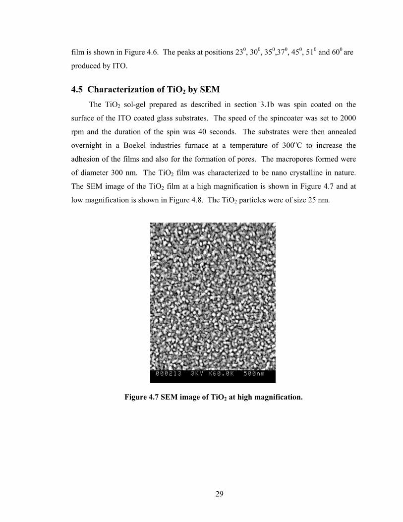
29
film is shown in Figure 4.6. The peaks at positions 230, 300, 350,370, 450, 510 and 600 are
produced by ITO.
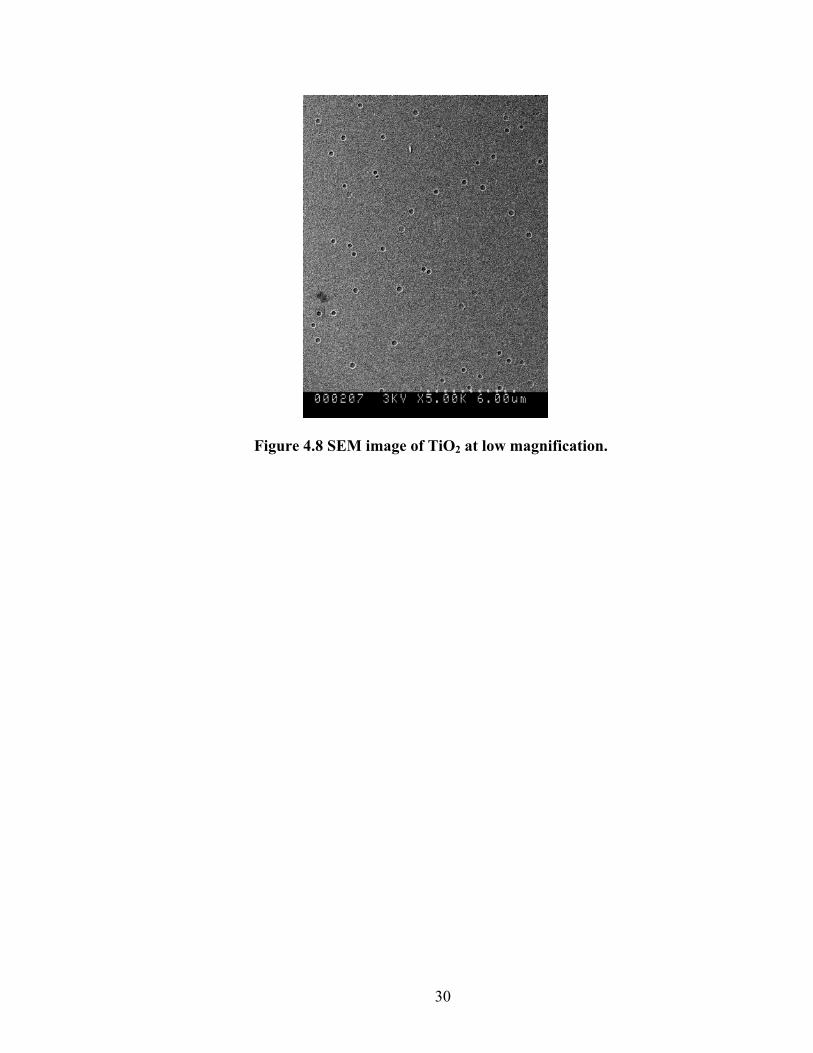
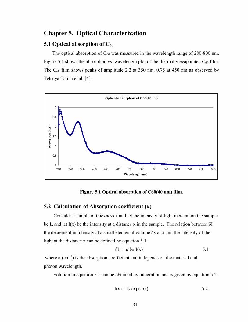
4.5 Characterization of TiO2 by SEM The TiO2 sol-gel prepared as described in section 3.1b was spin coated on the
surface of the ITO coated glass substrates. The speed of the spincoater was set to 2000
rpm and the duration of the spin was 40 seconds. The substrates were then annealed
overnight in a Boekel industries furnace at a temperature of 300oC to increase the
adhesion of the films and also for the formation of pores. The macropores formed were
of diameter 300 nm. The TiO2 film was characterized to be nano crystalline in nature.
The SEM image of the TiO2 film at a high magnification is shown in Figure 4.7 and at
low magnification is shown in Figure 4.8. The TiO2 particles were of size 25 nm.
Figure 4.7 SEM image of TiO2 at high magnification.
30
Figure 4.8 SEM image of TiO2 at low magnification.
31
Chapter 5. Optical Characterization 5.1 Optical absorption of C60 The optical absorption of C60 was measured in the wavelength range of 280-800 nm.
Figure 5.1 shows the absorption vs. wavelength plot of the thermally evaporated C60 film.
The C60 film shows peaks of amplitude 2.2 at 350 nm, 0.75 at 450 nm as observed by
Tetsuya Taima et al. [4].
Optical absorption of C60(40nm)
0
0.5
1
1.5
2
2.5
3
280 320 360 400 440 480 520 560 600 640 680 720 760 800
Wavelength (nm)
Abs
orpt
ion
(Abs
.)
Figure 5.1 Optical absorption of C60(40 nm) film.
5.2 Calculation of Absorption coefficient (α) Consider a sample of thickness x and let the intensity of light incident on the sample
be Io and let I(x) be the intensity at a distance x in the sample. The relation between δI
the decrement in intensity at a small elemental volume δx at x and the intensity of the
light at the distance x can be defined by equation 5.1.
δI = -α δx I(x) 5.1
where α (cm-1) is the absorption coefficient and it depends on the material and
photon wavelength.
Solution to equation 5.1 can be obtained by integration and is given by equation 5.2.
I(x) = Io exp(-αx) 5.2
32
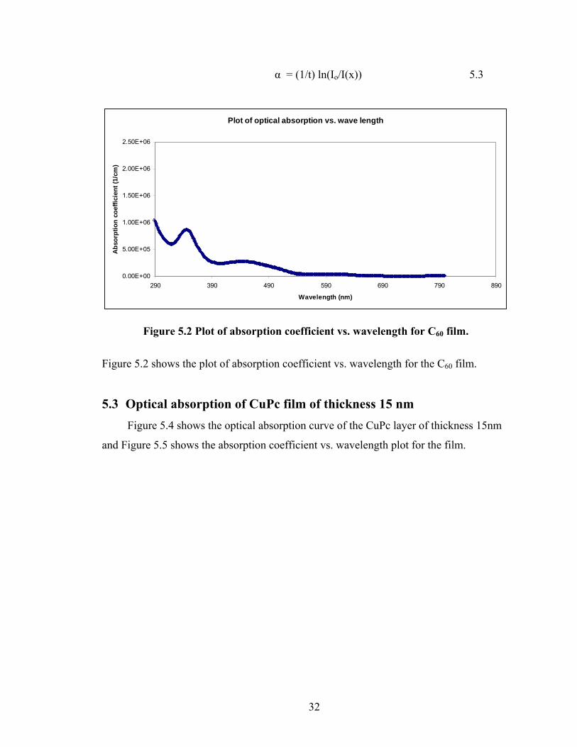
α = (1/t) ln(Io/I(x)) 5.3
Plot of optical absorption vs. wave length
0.00E+00
5.00E+05
1.00E+06
1.50E+06
2.00E+06
2.50E+06
290 390 490 590 690 790 890
Wavelength (nm)
Abs
orpt
ion
coef
ficie
nt (1
/cm
)
Figure 5.2 Plot of absorption coefficient vs. wavelength for C60 film.
Figure 5.2 shows the plot of absorption coefficient vs. wavelength for the C60 film.
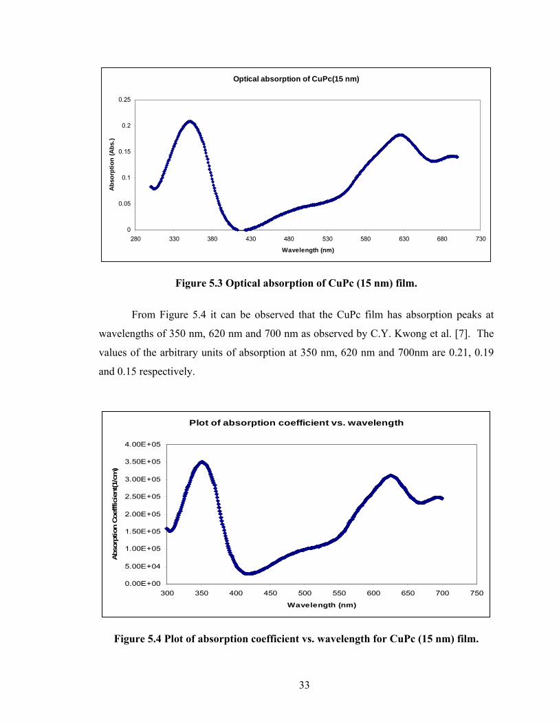
5.3 Optical absorption of CuPc film of thickness 15 nm Figure 5.4 shows the optical absorption curve of the CuPc layer of thickness 15nm
and Figure 5.5 shows the absorption coefficient vs. wavelength plot for the film.
33
Optical absorption of CuPc(15 nm)
0
0.05
0.1
0.15
0.2
0.25
280 330 380 430 480 530 580 630 680 730
Wavelength (nm)
Abs
orpt
ion
(Abs
.)
Figure 5.3 Optical absorption of CuPc (15 nm) film.
From Figure 5.4 it can be observed that the CuPc film has absorption peaks at
wavelengths of 350 nm, 620 nm and 700 nm as observed by C.Y. Kwong et al. [7]. The
values of the arbitrary units of absorption at 350 nm, 620 nm and 700nm are 0.21, 0.19
and 0.15 respectively.
Plot of absorption coefficient vs. wavelength
0.00E+00
5.00E+04
1.00E+05
1.50E+05
2.00E+05
2.50E+05
3.00E+05
3.50E+05
4.00E+05
300 350 400 450 500 550 600 650 700 750
Wavelength (nm)
Abso
rptio
n Co
efffi
cien
t(1/c
m)
Figure 5.4 Plot of absorption coefficient vs. wavelength for CuPc (15 nm) film.
34
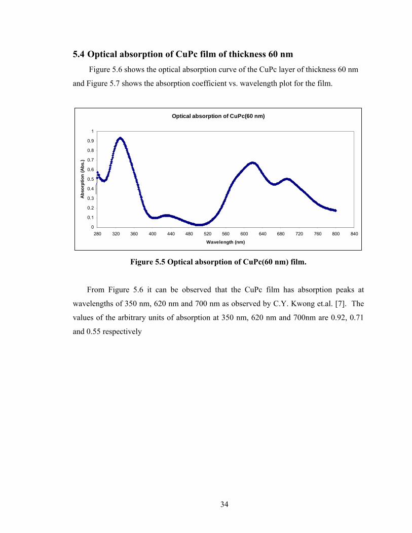
5.4 Optical absorption of CuPc film of thickness 60 nm Figure 5.6 shows the optical absorption curve of the CuPc layer of thickness 60 nm
and Figure 5.7 shows the absorption coefficient vs. wavelength plot for the film.
Optical absorption of CuPc(60 nm)
0
0.1
0.2
0.3
0.4
0.5
0.6
0.7
0.8
0.9
1
280 320 360 400 440 480 520 560 600 640 680 720 760 800 840
Wavelength (nm)
Abs
orpt
ion
(Abs
.)
Figure 5.5 Optical absorption of CuPc(60 nm) film.
From Figure 5.6 it can be observed that the CuPc film has absorption peaks at
wavelengths of 350 nm, 620 nm and 700 nm as observed by C.Y. Kwong et.al. [7]. The
values of the arbitrary units of absorption at 350 nm, 620 nm and 700nm are 0.92, 0.71
and 0.55 respectively
35
Plot of absorption coefficient vs. wavelength
0.00E+00
5.00E+04
1.00E+05
1.50E+05
2.00E+05
2.50E+05
3.00E+05
3.50E+05
4.00E+05
4.50E+05
5.00E+05
280 380 480 580 680 780
Wavelength (nm)
Abs
orpt
ion
coef
ficie
nt (1
/cm
)
Figure 5.6 Plot of absorption coefficient vs. wavelength for CuPc (60 nm) film.
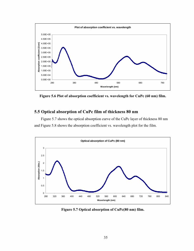
5.5 Optical absorption of CuPc film of thickness 80 nm Figure 5.7 shows the optical absorption curve of the CuPc layer of thickness 80 nm
and Figure 5.8 shows the absorption coefficient vs. wavelength plot for the film.
Optical absorption of CuPc (80 nm)
0
0.5
1
1.5
2
2.5
3
280 320 360 400 440 480 520 560 600 640 680 720 760 800 840
Wavelength (nm)
Abs
orpt
ion
(Abs
.)
Figure 5.7 Optical absorption of CuPc(80 nm) film.
36
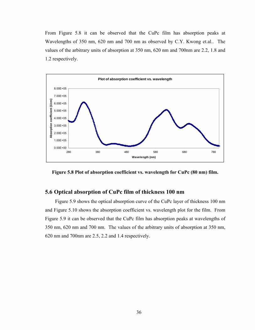
From Figure 5.8 it can be observed that the CuPc film has absorption peaks at
Wavelengths of 350 nm, 620 nm and 700 nm as observed by C.Y. Kwong et.al.. The
values of the arbitrary units of absorption at 350 nm, 620 nm and 700nm are 2.2, 1.8 and
1.2 respectively.
Plot of absorption coefficient vs. wavelength
0.00E+00
1.00E+05
2.00E+05
3.00E+05
4.00E+05
5.00E+05
6.00E+05
7.00E+05
8.00E+05
280 380 480 580 680 780
Wavelength (nm)
Abs
orpt
ion
coef
ficie
nt (1
/cm
)
Figure 5.8 Plot of absorption coefficient vs. wavelength for CuPc (80 nm) film. 5.6 Optical absorption of CuPc film of thickness 100 nm Figure 5.9 shows the optical absorption curve of the CuPc layer of thickness 100 nm
and Figure 5.10 shows the absorption coefficient vs. wavelength plot for the film. From
Figure 5.9 it can be observed that the CuPc film has absorption peaks at wavelengths of
350 nm, 620 nm and 700 nm. The values of the arbitrary units of absorption at 350 nm,
620 nm and 700nm are 2.5, 2.2 and 1.4 respectively.
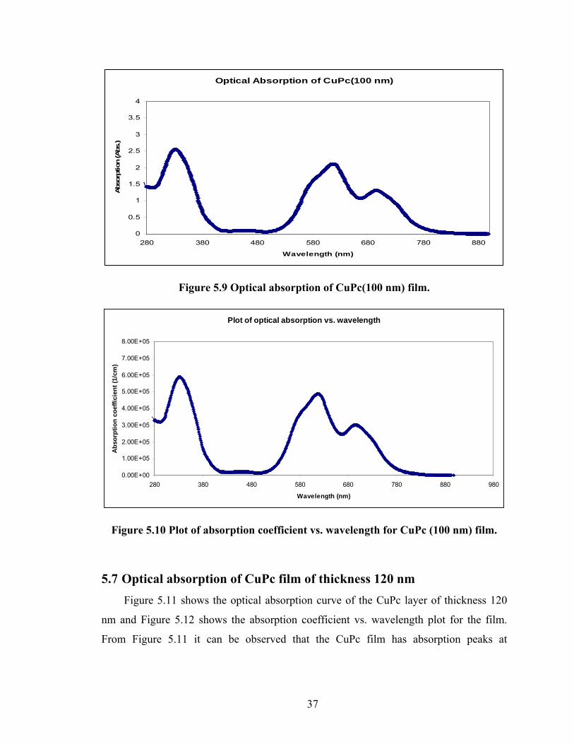
37
Optical Absorption of CuPc(100 nm)
0
0.5
1
1.5
2
2.5
3
3.5
4
280 380 480 580 680 780 880
Wavelength (nm)
Abso
rptio
n (A
bs.)
Figure 5.9 Optical absorption of CuPc(100 nm) film.
Plot of optical absorption vs. wavelength
0.00E+00
1.00E+05
2.00E+05
3.00E+05
4.00E+05
5.00E+05
6.00E+05
7.00E+05
8.00E+05
280 380 480 580 680 780 880 980
Wavelength (nm)
Abs
orpt
ion
coef
ficie
nt (1
/cm
)
Figure 5.10 Plot of absorption coefficient vs. wavelength for CuPc (100 nm) film.
5.7 Optical absorption of CuPc film of thickness 120 nm Figure 5.11 shows the optical absorption curve of the CuPc layer of thickness 120
nm and Figure 5.12 shows the absorption coefficient vs. wavelength plot for the film.
From Figure 5.11 it can be observed that the CuPc film has absorption peaks at
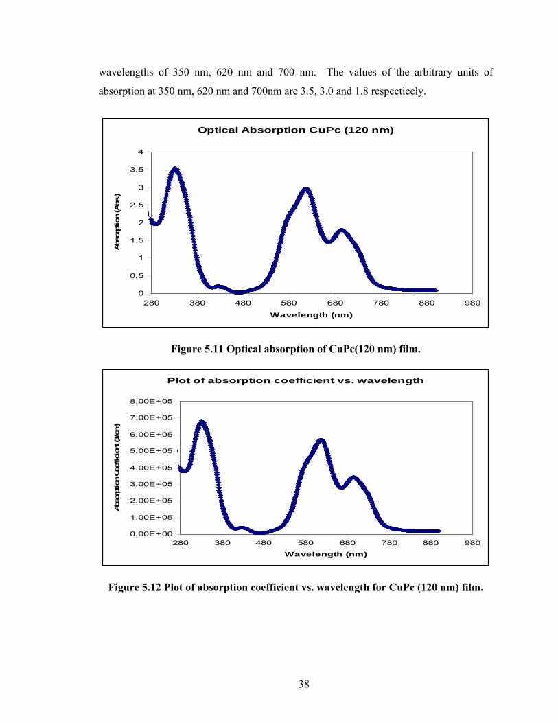
38
wavelengths of 350 nm, 620 nm and 700 nm. The values of the arbitrary units of
absorption at 350 nm, 620 nm and 700nm are 3.5, 3.0 and 1.8 respecticely.
Optical Absorption CuPc (120 nm)
0
0.5
1
1.5
2
2.5
3
3.5
4
280 380 480 580 680 780 880 980
Wavelength (nm)
Abs
orpt
ion
(Abs
.)
Figure 5.11 Optical absorption of CuPc(120 nm) film.
Plot of absorption coefficient vs. wavelength
0.00E+00
1.00E+05
2.00E+05
3.00E+05
4.00E+05
5.00E+05
6.00E+05
7.00E+05
8.00E+05
280 380 480 580 680 780 880 980
Wavelength (nm)
Abs
orpt
ion
Coeffic
ient
(1/cm
)
Figure 5.12 Plot of absorption coefficient vs. wavelength for CuPc (120 nm) film.
39
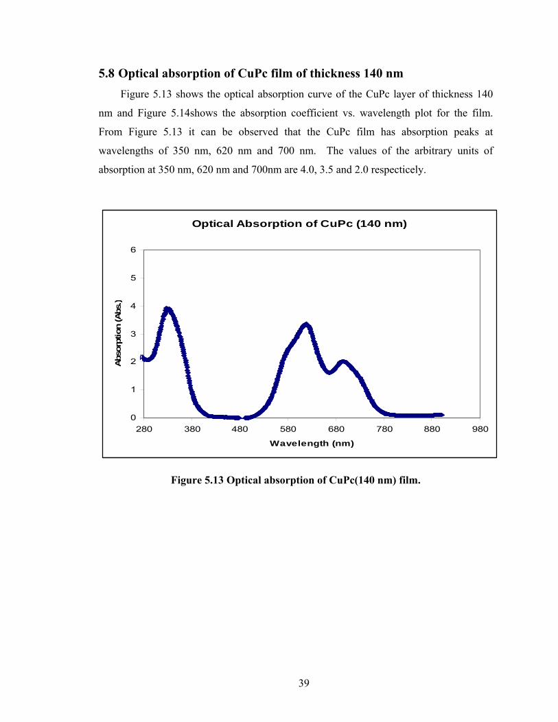
5.8 Optical absorption of CuPc film of thickness 140 nm Figure 5.13 shows the optical absorption curve of the CuPc layer of thickness 140
nm and Figure 5.14shows the absorption coefficient vs. wavelength plot for the film.
From Figure 5.13 it can be observed that the CuPc film has absorption peaks at
wavelengths of 350 nm, 620 nm and 700 nm. The values of the arbitrary units of
absorption at 350 nm, 620 nm and 700nm are 4.0, 3.5 and 2.0 respecticely.
Optical Absorption of CuPc (140 nm)
0
1
2
3
4
5
6
280 380 480 580 680 780 880 980
Wavelength (nm)
Abso
rptio
n (A
bs.)
Figure 5.13 Optical absorption of CuPc(140 nm) film.
40
Plot of absorption coefficient vs. wavelength
0.00E+00
1.00E+05
2.00E+05
3.00E+05
4.00E+05
5.00E+05
6.00E+05
7.00E+05
8.00E+05
9.00E+05
280 380 480 580 680 780 880 980
Wavelength (nm)
Abso
rptio
n Co
effic
ient
(1/cm
)
Figure 5.14 Plot of absorption coefficient vs. wavelength for CuPc (140 nm) film.
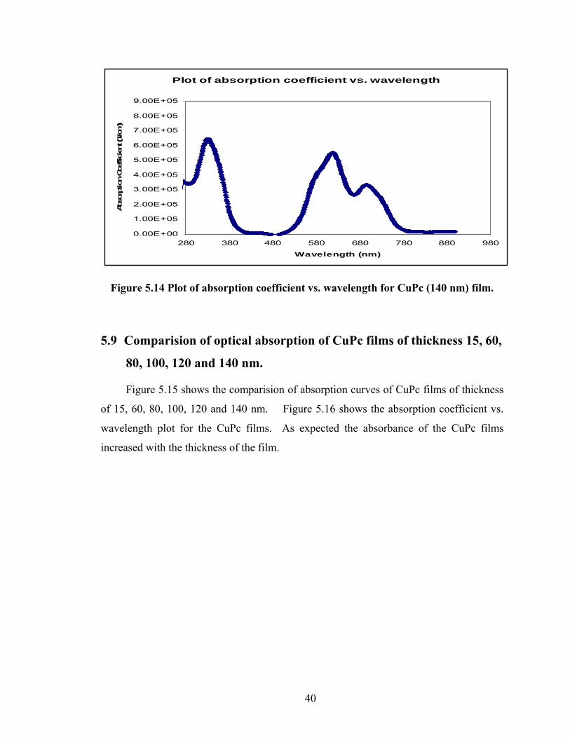
5.9 Comparision of optical absorption of CuPc films of thickness 15, 60,
80, 100, 120 and 140 nm. Figure 5.15 shows the comparision of absorption curves of CuPc films of thickness
of 15, 60, 80, 100, 120 and 140 nm. Figure 5.16 shows the absorption coefficient vs.
wavelength plot for the CuPc films. As expected the absorbance of the CuPc films
increased with the thickness of the film.

41
Optical absorption curves of CuPc thickness 15 nm, 60 nm, 80 nm, 100 nm, 120 nm, 140 nm
0
0.5
1
1.5
2
2.5
3
3.5
4
4.5
5
280 330 380 430 480 530 580 630 680 730 780
Wavelength (nm)
Abs
orpt
ion
(Abs
.) 15 nm60 nm80 nm100 nm120 nm140 nm
Figure 5.15 Optical absorption of CuPc films with thickness 15, 60, 80, 100, 120, 140
nm.
Plot of absorption vs. wavelength of CuPc films
0
200000
400000
600000
800000
1000000
1200000
1400000
280 380 480 580 680 780
Wavelength (nm)
Abs
orpt
ion
coef
ficie
nt (1
/cm
)
15 nm
60 nm
80 nm
100 nm
120 nm140 nm
Figure 5.16 Plot of absorption coefficient vs. wavelength for CuPc films with
thickness 15, 60, 80, 100, 120, 140 nm.
42
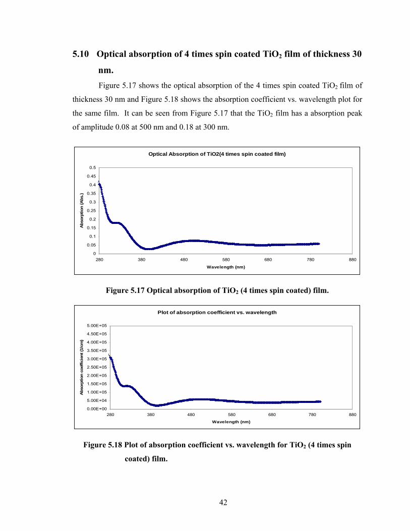
5.10 Optical absorption of 4 times spin coated TiO2 film of thickness 30
nm. Figure 5.17 shows the optical absorption of the 4 times spin coated TiO2 film of
thickness 30 nm and Figure 5.18 shows the absorption coefficient vs. wavelength plot for
the same film. It can be seen from Figure 5.17 that the TiO2 film has a absorption peak
of amplitude 0.08 at 500 nm and 0.18 at 300 nm.
Optical Absorption of TiO2(4 times spin coated film)
0
0.05
0.1
0.15
0.2
0.25
0.3
0.35
0.4
0.45
0.5
280 380 480 580 680 780 880
Wavelength (nm)
Abso
rptio
n (A
bs.)
Figure 5.17 Optical absorption of TiO2 (4 times spin coated) film.
Plot of absorption coefficient vs. wavelength
0.00E+00
5.00E+04
1.00E+05
1.50E+05
2.00E+05
2.50E+05
3.00E+05
3.50E+05
4.00E+05
4.50E+05
5.00E+05
280 380 480 580 680 780 880
Wavelength (nm)
Abso
rptio
n co
effic
ient
(1/c
m)
Figure 5.18 Plot of absorption coefficient vs. wavelength for TiO2 (4 times spin
coated) film.
43
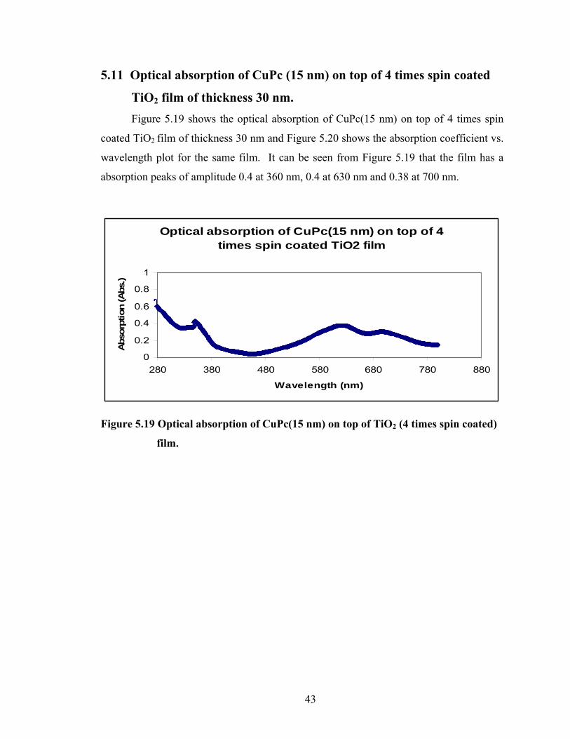
5.11 Optical absorption of CuPc (15 nm) on top of 4 times spin coated
TiO2 film of thickness 30 nm. Figure 5.19 shows the optical absorption of CuPc(15 nm) on top of 4 times spin
coated TiO2 film of thickness 30 nm and Figure 5.20 shows the absorption coefficient vs.
wavelength plot for the same film. It can be seen from Figure 5.19 that the film has a
absorption peaks of amplitude 0.4 at 360 nm, 0.4 at 630 nm and 0.38 at 700 nm.
Optical absorption of CuPc(15 nm) on top of 4 times spin coated TiO2 film
0
0.2
0.4
0.6
0.8
1
280 380 480 580 680 780 880
Wavelength (nm)
Abso
rptio
n (A
bs.)
Figure 5.19 Optical absorption of CuPc(15 nm) on top of TiO2 (4 times spin coated)
film.
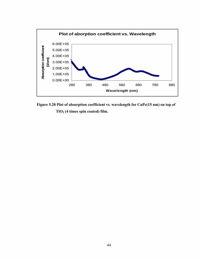
44
Plot of aborption coefficient vs. Wavelength
0.00E+00
1.00E+05
2.00E+05
3.00E+05
4.00E+05
5.00E+05
6.00E+05
280 380 480 580 680 780 880
Wavelength (nm)
Abs
orpt
ion
coef
ficie
nt
(1/c
m)
Figure 5.20 Plot of absorption coefficient vs. wavelength for CuPc(15 nm) on top of
TiO2 (4 times spin coated) film.
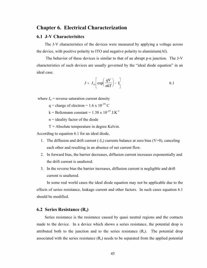
45
Chapter 6. Electrical Characterization 6.1 J-V Characterisitcs The J-V characteristics of the devices were measured by applying a voltage across
the device, with positive polarity to ITO and negative polarity to aluminium(Al).
The behavior of these devices is similar to that of an abrupt p-n junction. The J-V
characteristics of such devices are usually governed by the “ideal diode equation” in an
ideal case.
J JqVnkTO=
⎛⎝⎜
⎞⎠⎟ −
⎡
⎣⎢
⎤
⎦⎥exp 1 6.1
where Jo = reverse saturation current density
q = charge of electron = 1.6 x 10⁻¹⁹ C
k = Boltzmann constant = 1.38 x 10⁻²³ J.K-1
n = ideality factor of the diode
T = Absolute temperature in degree Kelvin.
According to equation 6.1 for an ideal diode,
1. The diffusion and drift current (-Jo) currents balance at zero bias (V=0), canceling
each other and resulting in an absence of net current flow.
2. In forward bias, the barrier decreases, diffusion current increases exponentially and
the drift current is unaltered.
3. In the reverse bias the barrier increases, diffusion current is negligible and drift
current is unaltered.
In some real world cases the ideal diode equation may not be applicable due to the
effects of series resistance, leakage current and other factors. In such cases equation 6.1
should be modified.
6.2 Series Resistance (Rs) Series resistance is the resistance caused by quasi neutral regions and the contacts
made to the device. In a device which shows a series resistance, the potential drop is
attributed both to the junction and to the series resistance (Rs). The potential drop
associated with the series resistance (Rs) needs to be separated from the applied potential
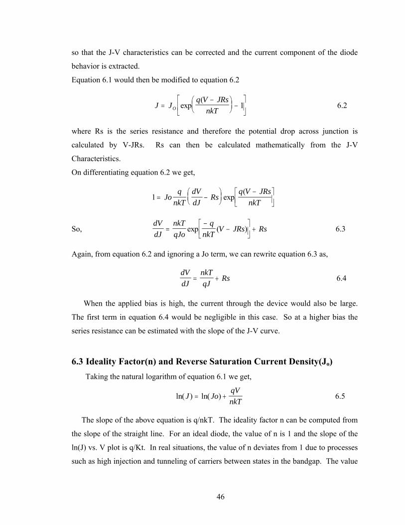
46
so that the J-V characteristics can be corrected and the current component of the diode
behavior is extracted.
Equation 6.1 would then be modified to equation 6.2
J Jq V JRs
nkTO=−⎛
⎝⎜⎞⎠⎟ −
⎡
⎣⎢
⎤
⎦⎥exp
(1 6.2
where Rs is the series resistance and therefore the potential drop across junction is
calculated by V-JRs. Rs can then be calculated mathematically from the J-V
Characteristics.
On differentiating equation 6.2 we get,
1 = −⎛⎝⎜
⎞⎠⎟
−⎡⎣⎢
⎤⎦⎥
Joq
nkTdVdJ
Rsq V JRs
nkTexp
(
So, dVdJ
nkTqJo
qnkT
V JRs Rs=−
−⎡⎣⎢
⎤⎦⎥+exp ( ) 6.3
Again, from equation 6.2 and ignoring a Jo term, we can rewrite equation 6.3 as,
dVdJ
nkTqJ
Rs= + 6.4
When the applied bias is high, the current through the device would also be large.
The first term in equation 6.4 would be negligible in this case. So at a higher bias the
series resistance can be estimated with the slope of the J-V curve.
6.3 Ideality Factor(n) and Reverse Saturation Current Density(Jo) Taking the natural logarithm of equation 6.1 we get,
ln( ) ln( )J JoqVnkT
= + 6.5
The slope of the above equation is q/nkT. The ideality factor n can be computed from
the slope of the straight line. For an ideal diode, the value of n is 1 and the slope of the
ln(J) vs. V plot is q/Kt. In real situations, the value of n deviates from 1 due to processes
such as high injection and tunneling of carriers between states in the bandgap. The value
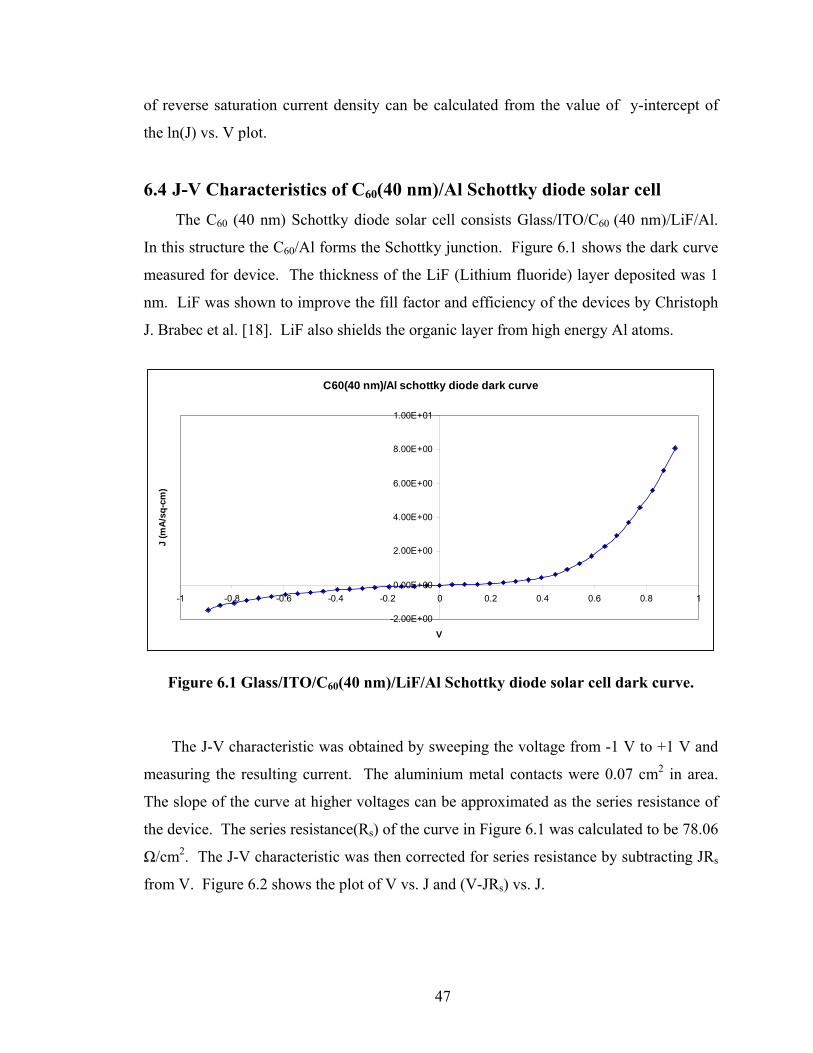
47
of reverse saturation current density can be calculated from the value of y-intercept of
the ln(J) vs. V plot.
6.4 J-V Characteristics of C60(40 nm)/Al Schottky diode solar cell The C60 (40 nm) Schottky diode solar cell consists Glass/ITO/C60 (40 nm)/LiF/Al.
In this structure the C60/Al forms the Schottky junction. Figure 6.1 shows the dark curve
measured for device. The thickness of the LiF (Lithium fluoride) layer deposited was 1
nm. LiF was shown to improve the fill factor and efficiency of the devices by Christoph
J. Brabec et al. [18]. LiF also shields the organic layer from high energy Al atoms.
C60(40 nm)/Al schottky diode dark curve
-2.00E+00
0.00E+00
2.00E+00
4.00E+00
6.00E+00
8.00E+00
1.00E+01
-1 -0.8 -0.6 -0.4 -0.2 0 0.2 0.4 0.6 0.8 1
V
J (m
A/s
q-cm
)
Figure 6.1 Glass/ITO/C60(40 nm)/LiF/Al Schottky diode solar cell dark curve.
The J-V characteristic was obtained by sweeping the voltage from -1 V to +1 V and
measuring the resulting current. The aluminium metal contacts were 0.07 cm2 in area.
The slope of the curve at higher voltages can be approximated as the series resistance of
the device. The series resistance(Rs) of the curve in Figure 6.1 was calculated to be 78.06
Ω/cm2. The J-V characteristic was then corrected for series resistance by subtracting JRs
from V. Figure 6.2 shows the plot of V vs. J and (V-JRs) vs. J.
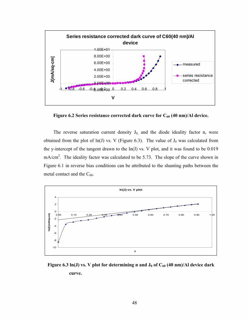
48
Series resistance corrected dark curve of C60(40 nm)/Al device
-2.00E+00
0.00E+00
2.00E+00
4.00E+00
6.00E+00
8.00E+00
1.00E+01
-1 -0.8 -0.6 -0.4 -0.2 0 0.2 0.4 0.6 0.8 1
V
J(m
A/s
q-cm
)
measured
series resistancecorrected
Figure 6.2 Series resistance corrected dark curve for C60 (40 nm)/Al device.
The reverse saturation current density J0, and the diode ideality factor n, were
obtained from the plot of ln(J) vs. V (Figure 6.3). The value of J0 was calculated from
the y-intercept of the tangent drawn to the ln(J) vs. V plot, and it was found to be 0.019
mA/cm2. The ideality factor was calculated to be 5.73. The slope of the curve shown in
Figure 6.1 in reverse bias conditions can be attributed to the shunting paths between the
metal contact and the C60.
ln(J) vs. V plot
-10
-8
-6
-4
-2
0
2
4
0.00 0.10 0.20 0.30 0.40 0.50 0.60 0.70 0.80 0.90 1.00
V
ln(J
) (m
A/s
q-cm
)
Figure 6.3 ln(J) vs. V plot for determining n and J0 of C60 (40 nm)/Al device dark
curve.
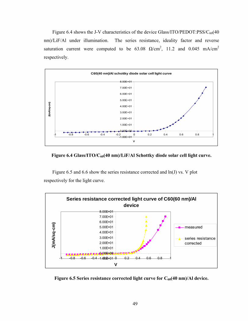
49
Figure 6.4 shows the J-V characteristics of the device Glass/ITO/PEDOT:PSS/C60(40
nm)/LiF/Al under illumination. The series resistance, ideality factor and reverse
saturation current were computed to be 63.08 Ω/cm2, 11.2 and 0.045 mA/cm2
respectively.
C60(40 nm)/Al schottky diode solar cell light curve
-1.00E+01
0.00E+00
1.00E+01
2.00E+01
3.00E+01
4.00E+01
5.00E+01
6.00E+01
7.00E+01
8.00E+01
-1 -0.8 -0.6 -0.4 -0.2 0 0.2 0.4 0.6 0.8 1
V
J(m
A/s
q-cm
)
Figure 6.4 Glass/ITO/C60(40 nm)/LiF/Al Schottky diode solar cell light curve.
Figure 6.5 and 6.6 show the series resistance corrected and ln(J) vs. V plot
respectively for the light curve.
Series resistance corrected light curve of C60(60 nm)/Al device
-1.00E+010.00E+001.00E+012.00E+013.00E+014.00E+015.00E+016.00E+017.00E+018.00E+01
-1 -0.8 -0.6 -0.4 -0.2 0 0.2 0.4 0.6 0.8 1
V
J(m
A/s
q-cm
)
measured
series resistancecorrected
Figure 6.5 Series resistance corrected light curve for C60(40 nm)/Al device.
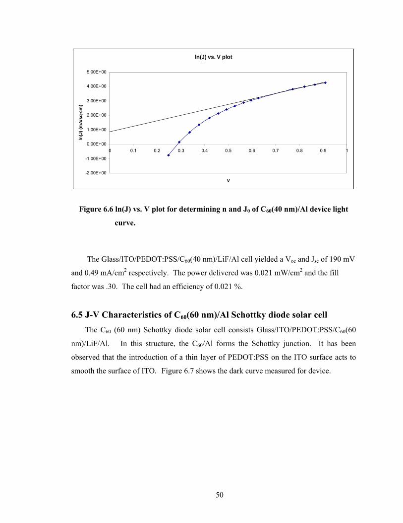
50
ln(J) vs. V plot
-2.00E+00
-1.00E+00
0.00E+00
1.00E+00
2.00E+00
3.00E+00
4.00E+00
5.00E+00
0 0.1 0.2 0.3 0.4 0.5 0.6 0.7 0.8 0.9 1
V
ln(J
) (m
A/sq
-cm
)
Figure 6.6 ln(J) vs. V plot for determining n and J0 of C60(40 nm)/Al device light
curve.
The Glass/ITO/PEDOT:PSS/C60(40 nm)/LiF/Al cell yielded a Voc and Jsc of 190 mV
and 0.49 mA/cm2 respectively. The power delivered was 0.021 mW/cm2 and the fill
factor was .30. The cell had an efficiency of 0.021 %.
6.5 J-V Characteristics of C60(60 nm)/Al Schottky diode solar cell The C60 (60 nm) Schottky diode solar cell consists Glass/ITO/PEDOT:PSS/C60(60
nm)/LiF/Al. In this structure, the C60/Al forms the Schottky junction. It has been
observed that the introduction of a thin layer of PEDOT:PSS on the ITO surface acts to
smooth the surface of ITO. Figure 6.7 shows the dark curve measured for device.
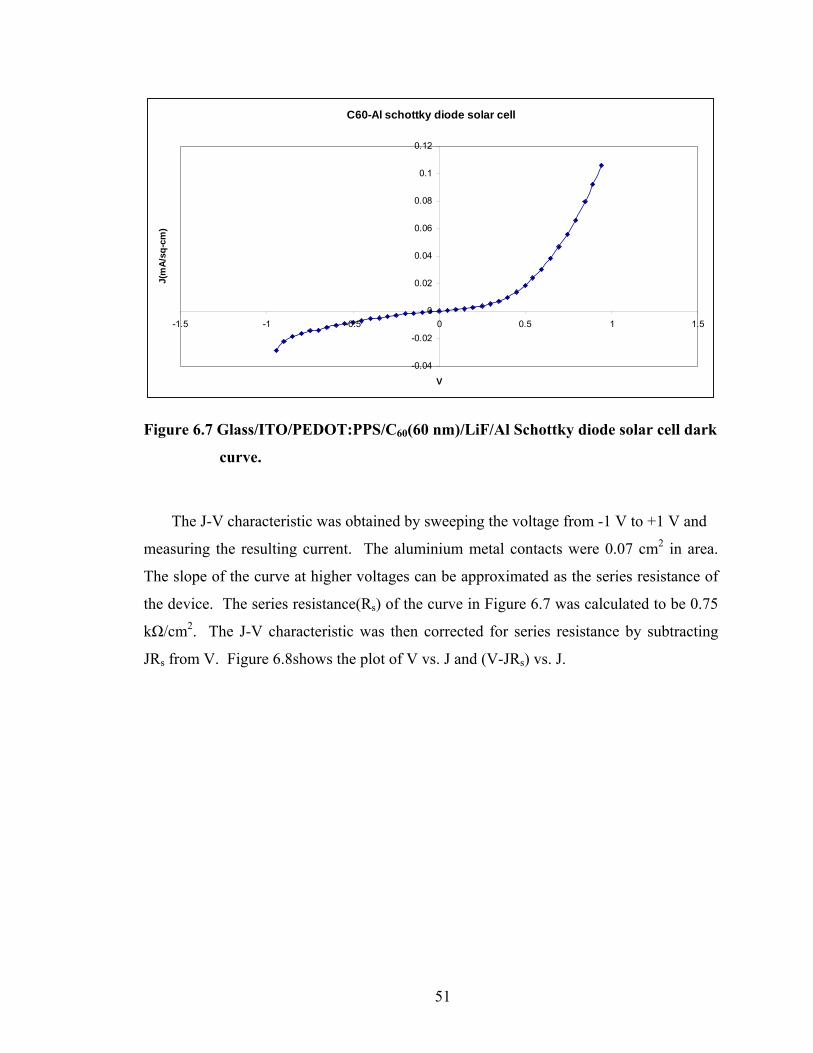
51
C60-Al schottky diode solar cell
-0.04
-0.02
0
0.02
0.04
0.06
0.08
0.1
0.12
-1.5 -1 -0.5 0 0.5 1 1.5
V
J(m
A/sq
-cm
)
Figure 6.7 Glass/ITO/PEDOT:PPS/C60(60 nm)/LiF/Al Schottky diode solar cell dark
curve.
The J-V characteristic was obtained by sweeping the voltage from -1 V to +1 V and
measuring the resulting current. The aluminium metal contacts were 0.07 cm2 in area.
The slope of the curve at higher voltages can be approximated as the series resistance of
the device. The series resistance(Rs) of the curve in Figure 6.7 was calculated to be 0.75
kΩ/cm2. The J-V characteristic was then corrected for series resistance by subtracting
JRs from V. Figure 6.8shows the plot of V vs. J and (V-JRs) vs. J.
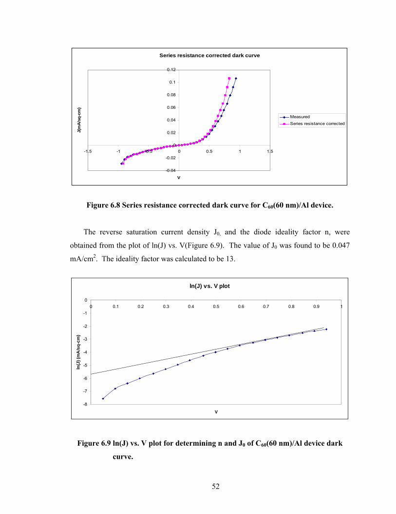
52
Series resistance corrected dark curve
-0.04
-0.02
0
0.02
0.04
0.06
0.08
0.1
0.12
-1.5 -1 -0.5 0 0.5 1 1.5
V
J(m
A/sq
-cm
)
MeasuredSeries resistance corrected
Figure 6.8 Series resistance corrected dark curve for C60(60 nm)/Al device.
The reverse saturation current density J0, and the diode ideality factor n, were
obtained from the plot of ln(J) vs. V(Figure 6.9). The value of J0 was found to be 0.047
mA/cm2. The ideality factor was calculated to be 13.
ln(J) vs. V plot
-8
-7
-6
-5
-4
-3
-2
-1
00 0.1 0.2 0.3 0.4 0.5 0.6 0.7 0.8 0.9 1
V
ln(J
) (m
A/s
q-cm
)
Figure 6.9 ln(J) vs. V plot for determining n and J0 of C60(60 nm)/Al device dark
curve.
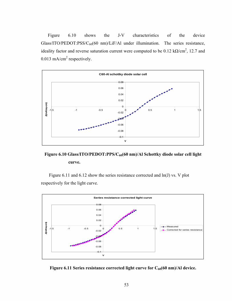
53
Figure 6.10 shows the J-V characteristics of the device
Glass/ITO/PEDOT:PSS/C60(60 nm)/LiF/Al under illumination. The series resistance,
ideality factor and reverse saturation current were computed to be 0.12 kΩ/cm2, 12.7 and
0.013 mA/cm2 respectively.
C60-Al schottky diode solar cell
-0.1
-0.08
-0.06
-0.04
-0.02
0
0.02
0.04
0.06
0.08
-1.5 -1 -0.5 0 0.5 1 1.5
V
J(m
A/sq
-cm
)
Figure 6.10 Glass/ITO/PEDOT:PPS/C60(60 nm)/Al Schottky diode solar cell light
curve.
Figure 6.11 and 6.12 show the series resistance corrected and ln(J) vs. V plot
respectively for the light curve.
Series resistance corrected light curve
-0.1
-0.08
-0.06
-0.04
-0.02
0
0.02
0.04
0.06
0.08
-1.5 -1 -0.5 0 0.5 1 1.5
V
J(m
A/sq
-cm
)
MeasuredCorrected for series resistance
Figure 6.11 Series resistance corrected light curve for C60(60 nm)/Al device.
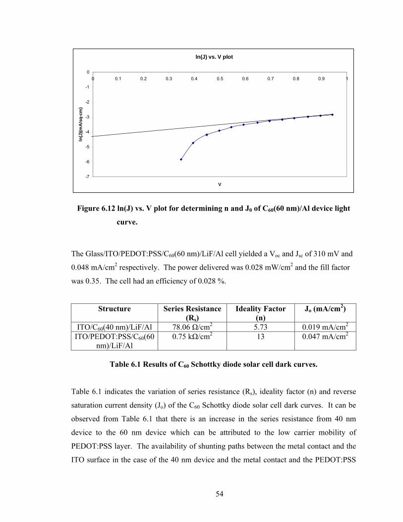
54
ln(J) vs. V plot
-7
-6
-5
-4
-3
-2
-1
00 0.1 0.2 0.3 0.4 0.5 0.6 0.7 0.8 0.9 1
V
ln(J
)(mA/
sq-c
m)
Figure 6.12 ln(J) vs. V plot for determining n and J0 of C60(60 nm)/Al device light
curve.
The Glass/ITO/PEDOT:PSS/C60(60 nm)/LiF/Al cell yielded a Voc and Jsc of 310 mV and
0.048 mA/cm2 respectively. The power delivered was 0.028 mW/cm2 and the fill factor
was 0.35. The cell had an efficiency of 0.028 %.
Structure Series Resistance (Rs)
Ideality Factor (n)
Jo (mA/cm2)
ITO/C60(40 nm)/LiF/Al 78.06 Ω/cm2 5.73 0.019 mA/cm2 ITO/PEDOT:PSS/C60(60
nm)/LiF/Al 0.75 kΩ/cm2 13 0.047 mA/cm2
Table 6.1 Results of C60 Schottky diode solar cell dark curves.
Table 6.1 indicates the variation of series resistance (Rs), ideality factor (n) and reverse
saturation current density (Jo) of the C60 Schottky diode solar cell dark curves. It can be
observed from Table 6.1 that there is an increase in the series resistance from 40 nm
device to the 60 nm device which can be attributed to the low carrier mobility of
PEDOT:PSS layer. The availability of shunting paths between the metal contact and the
ITO surface in the case of the 40 nm device and the metal contact and the PEDOT:PSS

55
layer in case of the 60 nm device can be the reason for the curves having a slope in the
reverse bias conditions.
Structure Rs n Jo Voc Jsc
F.F. P. D. η
ITO/C60(40 nm)/LiF/Al
63.08 Ω/cm2
11.2 0.045 mA/cm2
190 mV
0.49 mA/cm2
0.30 0.021 mW/cm2
0.021%
ITO/PEDOT:PSS/C60(60 nm)/LiF/Al
0.12 kΩ/cm2
12.7 0.013 mA/cm2
310 mV
0.48 mA/cm2
0.35 0.028 mW/cm2
0.028%
Table 6.2 Results of C60 Schottky diode solar cell light curves.
Table 6.2 indicates the variation of series resistance (Rs), ideality factor (n), reverse
saturation current density (Jo), open circuit voltage (Voc), short circuit current (Jsc), fill
factor, power delivered by the cell and the efficiency of the cell. As in the case of dark
curves the series resistance of the cells under illumination also increased due to the
inclusion of PEDOT:PSS layer in case of the 60 nm device. The high reverse saturation
currents suggest the presence of physical shunting paths. PEDOT:PSS was included to
smooth out the irregularities in the ITO surface which in turn leads to the formation of a
uniform C60 film. With the increase in the thickness of the C60 layer the open circuit
voltage (Voc) increases by 120 mV. This increase in Voc can be attributed to the increase
in the absorption of C60 film when the thickness is increased from 40 nm to 60 nm. In
case of the short circuit current (Jsc) we did not observe much change and this can be
attributed to the increase in the series resistance from 40 nm to 60 nm device. We
observed an increase in the fill factor, power delivered and efficiency in case of the 60
nm device. The high diode ideality factors indicate several transport mechanisms like
recombination-generation currents in the depletion region and recombination through
interface states at the junction.
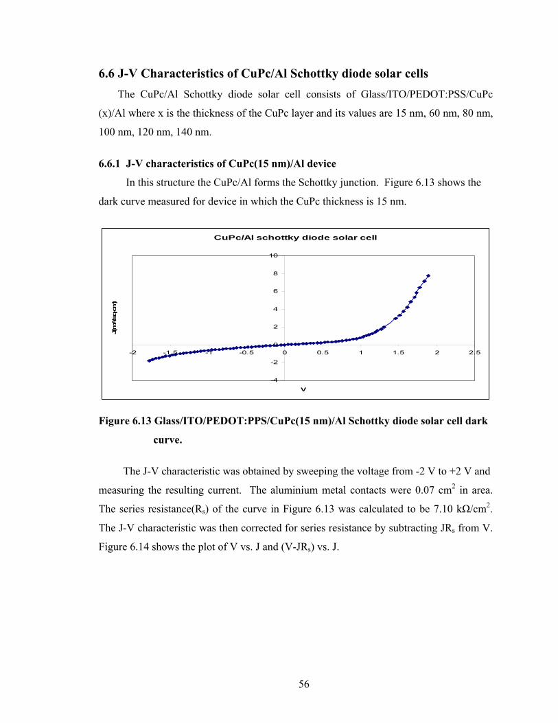
56
6.6 J-V Characteristics of CuPc/Al Schottky diode solar cells The CuPc/Al Schottky diode solar cell consists of Glass/ITO/PEDOT:PSS/CuPc
(x)/Al where x is the thickness of the CuPc layer and its values are 15 nm, 60 nm, 80 nm,
100 nm, 120 nm, 140 nm.
6.6.1 J-V characteristics of CuPc(15 nm)/Al device
In this structure the CuPc/Al forms the Schottky junction. Figure 6.13 shows the
dark curve measured for device in which the CuPc thickness is 15 nm.
CuPc/Al schottky diode solar cell
-4
-2
0
2
4
6
8
10
-2 -1.5 -1 -0.5 0 0.5 1 1.5 2 2.5
V
J(m
A/sq-
cm)
Figure 6.13 Glass/ITO/PEDOT:PPS/CuPc(15 nm)/Al Schottky diode solar cell dark
curve.
The J-V characteristic was obtained by sweeping the voltage from -2 V to +2 V and
measuring the resulting current. The aluminium metal contacts were 0.07 cm2 in area.
The series resistance(Rs) of the curve in Figure 6.13 was calculated to be 7.10 kΩ/cm2.
The J-V characteristic was then corrected for series resistance by subtracting JRs from V.
Figure 6.14 shows the plot of V vs. J and (V-JRs) vs. J.
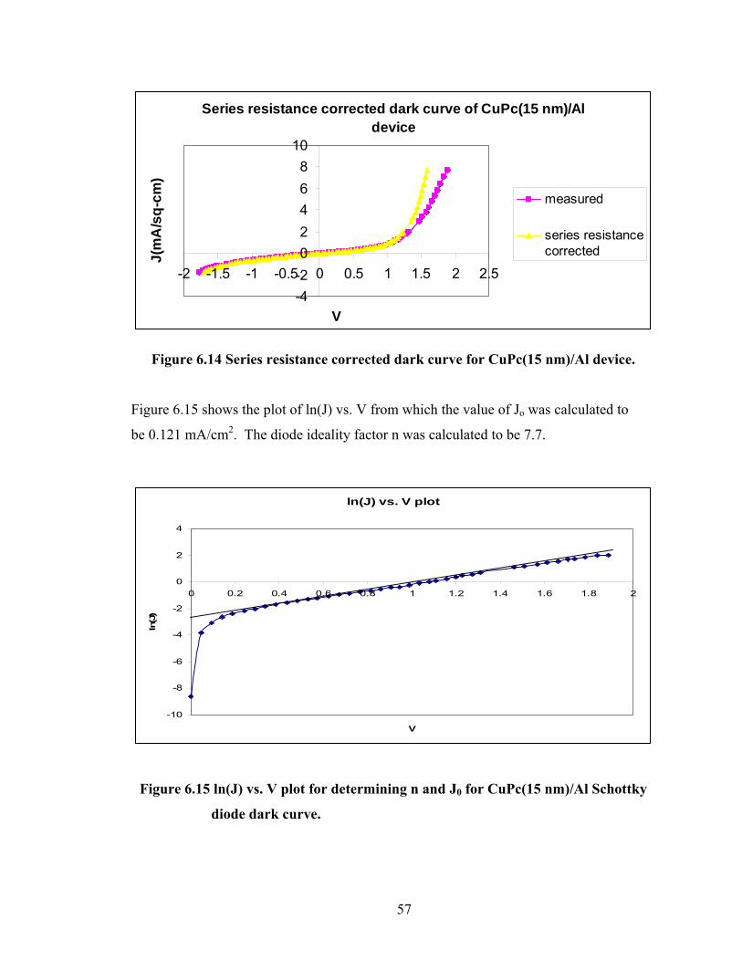
57
Series resistance corrected dark curve of CuPc(15 nm)/Al device
-4-202468
10
-2 -1.5 -1 -0.5 0 0.5 1 1.5 2 2.5
V
J(m
A/s
q-cm
)
measured
series resistancecorrected
Figure 6.14 Series resistance corrected dark curve for CuPc(15 nm)/Al device. Figure 6.15 shows the plot of ln(J) vs. V from which the value of Jo was calculated to
be 0.121 mA/cm2. The diode ideality factor n was calculated to be 7.7.
ln(J) vs. V plot
-10
-8
-6
-4
-2
0
2
4
0 0.2 0.4 0.6 0.8 1 1.2 1.4 1.6 1.8 2
V
ln(J
)
Figure 6.15 ln(J) vs. V plot for determining n and J0 for CuPc(15 nm)/Al Schottky
diode dark curve.
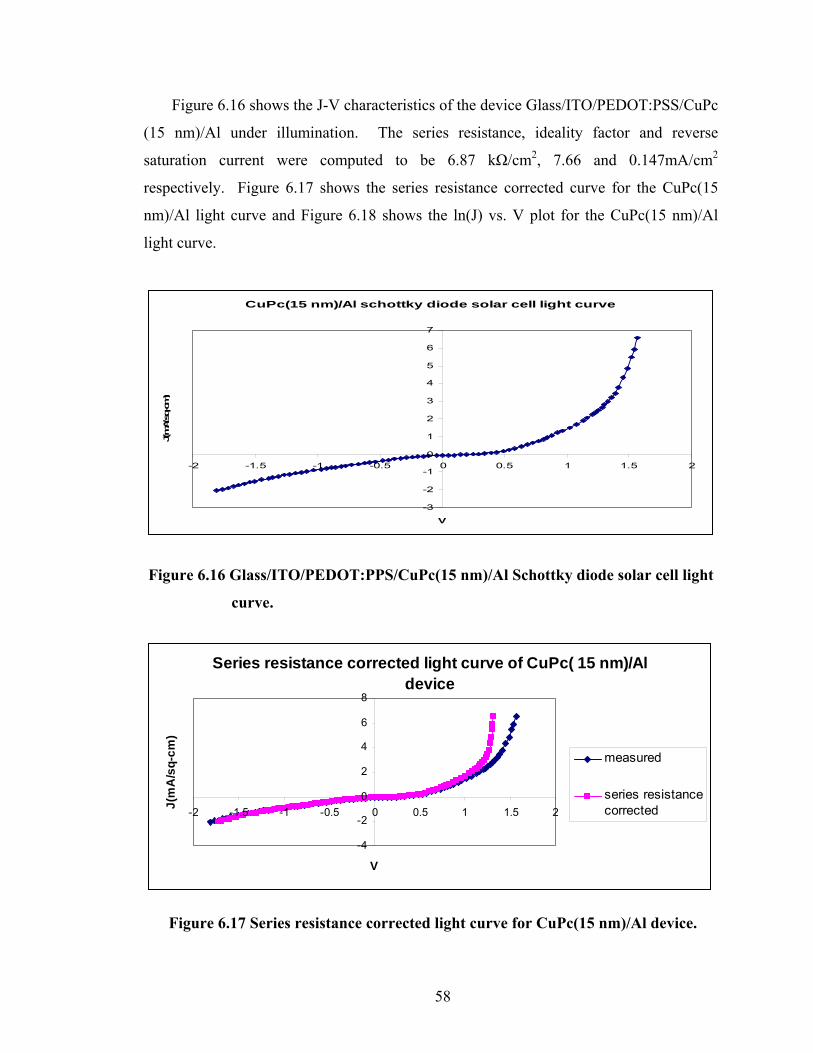
58
Figure 6.16 shows the J-V characteristics of the device Glass/ITO/PEDOT:PSS/CuPc
(15 nm)/Al under illumination. The series resistance, ideality factor and reverse
saturation current were computed to be 6.87 kΩ/cm2, 7.66 and 0.147mA/cm2
respectively. Figure 6.17 shows the series resistance corrected curve for the CuPc(15
nm)/Al light curve and Figure 6.18 shows the ln(J) vs. V plot for the CuPc(15 nm)/Al
light curve.
CuPc(15 nm)/Al schottky diode solar cell light curve
-3
-2
-1
0
1
2
3
4
5
6
7
-2 -1.5 -1 -0.5 0 0.5 1 1.5 2
V
J(m
A/sq
-cm
)
Figure 6.16 Glass/ITO/PEDOT:PPS/CuPc(15 nm)/Al Schottky diode solar cell light
curve.
Series resistance corrected light curve of CuPc( 15 nm)/Al device
-4
-2
0
2
4
6
8
-2 -1.5 -1 -0.5 0 0.5 1 1.5 2
V
J(m
A/s
q-cm
)
measured
series resistancecorrected
Figure 6.17 Series resistance corrected light curve for CuPc(15 nm)/Al device.
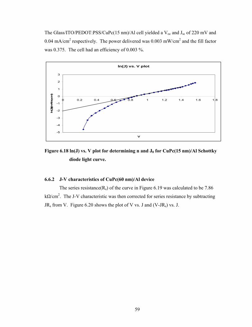
59
The Glass/ITO/PEDOT:PSS/CuPc(15 nm)/Al cell yielded a Voc and Jsc of 220 mV and
0.04 mA/cm2 respectively. The power delivered was 0.003 mW/cm2 and the fill factor
was 0.375. The cell had an efficiency of 0.003 %.
ln(J) vs. V plot
-5
-4
-3
-2
-1
0
1
2
3
0 0.2 0.4 0.6 0.8 1 1.2 1.4 1.6 1.8
V
ln(J
)(mA/
sq-c
m)
Figure 6.18 ln(J) vs. V plot for determining n and J0 for CuPc(15 nm)/Al Schottky
diode light curve.
6.6.2 J-V characteristics of CuPc(60 nm)/Al device
The series resistance(Rs) of the curve in Figure 6.19 was calculated to be 7.86
kΩ/cm2. The J-V characteristic was then corrected for series resistance by subtracting
JRs from V. Figure 6.20 shows the plot of V vs. J and (V-JRs) vs. J.
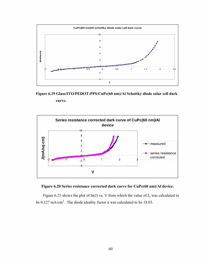
60
CuPc(60 nm)/Al schottky diode solar cell dark curve
-4
-2
0
2
4
6
8
10
-2 -1.5 -1 -0.5 0 0.5 1 1.5 2 2.5
V
J(m
A/sq
-cm
)
Figure 6.19 Glass/ITO/PEDOT:PPS/CuPc(60 nm)/Al Schottky diode solar cell dark
curve.
Series resistance corrected dark curve of CuPc(60 nm)/Al device
-4
-2
0
2
4
6
8
10
-2 -1 0 1 2 3
V
J(m
A/s
q-cm
)
measured
series resistancecorrected
Figure 6.20 Series resistance corrected dark curve for CuPc(60 nm)/Al device. Figure 6.21 shows the plot of ln(J) vs. V from which the value of Jo was calculated to
be 0.127 mA/cm2. The diode ideality factor n was calculated to be 18.03.
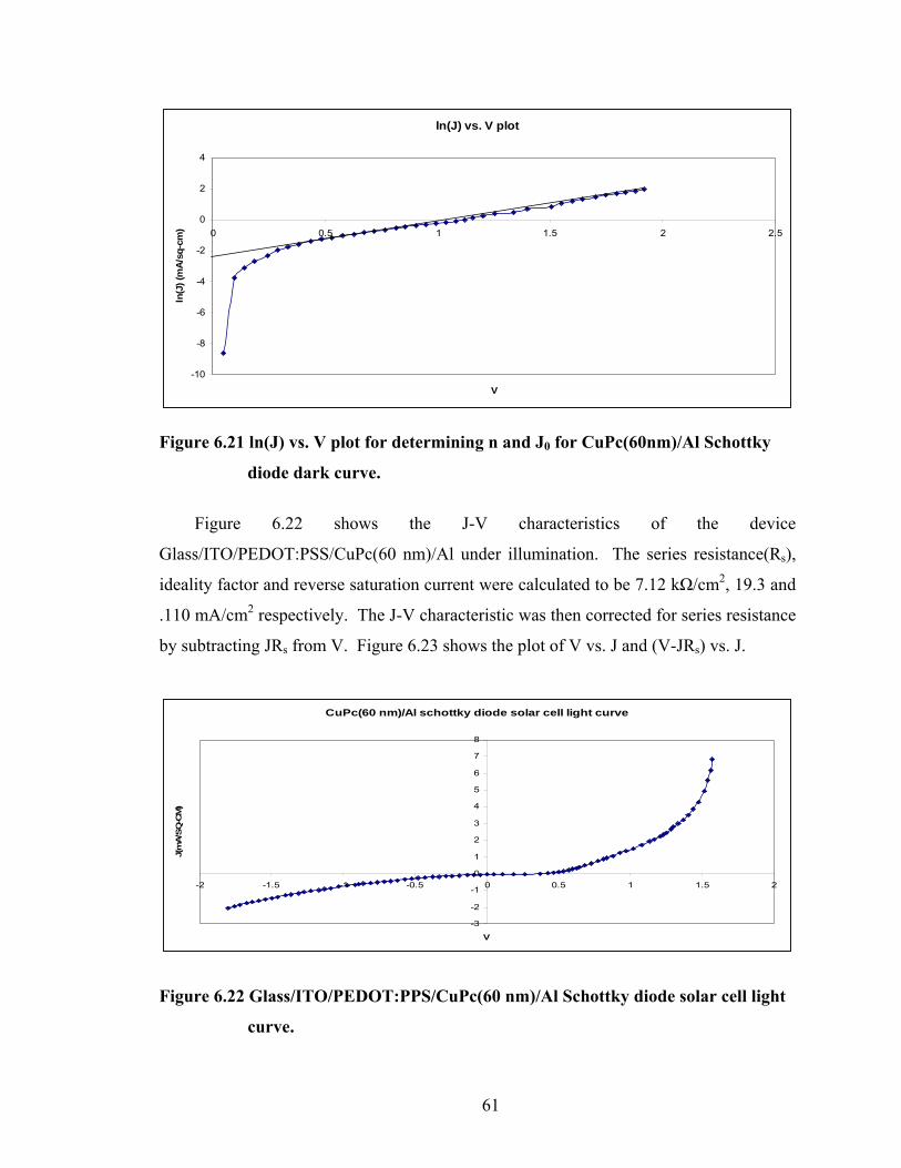
61
ln(J) vs. V plot
-10
-8
-6
-4
-2
0
2
4
0 0.5 1 1.5 2 2.5
V
ln(J
) (m
A/sq
-cm
)
Figure 6.21 ln(J) vs. V plot for determining n and J0 for CuPc(60nm)/Al Schottky
diode dark curve.
Figure 6.22 shows the J-V characteristics of the device
Glass/ITO/PEDOT:PSS/CuPc(60 nm)/Al under illumination. The series resistance(Rs),
ideality factor and reverse saturation current were calculated to be 7.12 kΩ/cm2, 19.3 and
.110 mA/cm2 respectively. The J-V characteristic was then corrected for series resistance
by subtracting JRs from V. Figure 6.23 shows the plot of V vs. J and (V-JRs) vs. J.
CuPc(60 nm)/Al schottky diode solar cell light curve
-3
-2
-1
0
1
2
3
4
5
6
7
8
-2 -1.5 -1 -0.5 0 0.5 1 1.5 2
V
J(m
A/SQ
-CM
)
Figure 6.22 Glass/ITO/PEDOT:PPS/CuPc(60 nm)/Al Schottky diode solar cell light
curve.
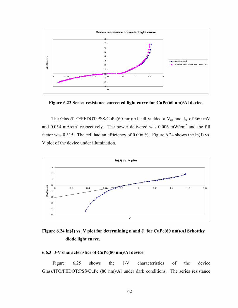
62
Series resistance corrected light curve
-3
-2
-1
0
1
2
3
4
5
6
7
8
-2 -1.5 -1 -0.5 0 0.5 1 1.5 2
V
J(m
A/s
q-cm
)
measuredseries resistance corrected
Figure 6.23 Series resistance corrected light curve for CuPc(60 nm)/Al device.
The Glass/ITO/PEDOT:PSS/CuPc(60 nm)/Al cell yielded a Voc and Jsc of 360 mV
and 0.054 mA/cm2 respectively. The power delivered was 0.006 mW/cm2 and the fill
factor was 0.315. The cell had an efficiency of 0.006 %. Figure 6.24 shows the ln(J) vs.
V plot of the device under illumination.
ln(J) vs. V plot
-5
-4
-3
-2
-1
0
1
2
3
0 0.2 0.4 0.6 0.8 1 1.2 1.4 1.6 1.8
V
J(m
A/s
q-cm
)
Figure 6.24 ln(J) vs. V plot for determining n and J0 for CuPc(60 nm)/Al Schottky
diode light curve.
6.6.3 J-V characteristics of CuPc(80 nm)/Al device Figure 6.25 shows the J-V characteristics of the device
Glass/ITO/PEDOT:PSS/CuPc (80 nm)/Al under dark conditions. The series resistance
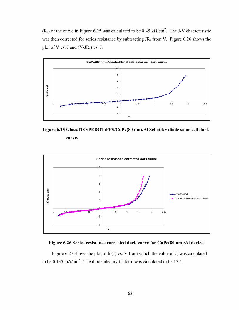
63
(Rs) of the curve in Figure 6.25 was calculated to be 8.45 kΩ/cm2. The J-V characteristic
was then corrected for series resistance by subtracting JRs from V. Figure 6.26 shows the
plot of V vs. J and (V-JRs) vs. J.
CuPc(80 nm)/Al schottky diode solar cell dark curve
-4
-2
0
2
4
6
8
10
-2 -1.5 -1 -0.5 0 0.5 1 1.5 2 2.5
V
J(m
A/s
q-cm
)
Figure 6.25 Glass/ITO/PEDOT:PPS/CuPc(80 nm)/Al Schottky diode solar cell dark
curve.
Series resistance corrected dark curve
-4
-2
0
2
4
6
8
10
-2 -1.5 -1 -0.5 0 0.5 1 1.5 2 2.5
V
J(m
A/sq
-cm
)
measuredseries resistance corrected
Figure 6.26 Series resistance corrected dark curve for CuPc(80 nm)/Al device.
Figure 6.27 shows the plot of ln(J) vs. V from which the value of Jo was calculated
to be 0.135 mA/cm2. The diode ideality factor n was calculated to be 17.5.
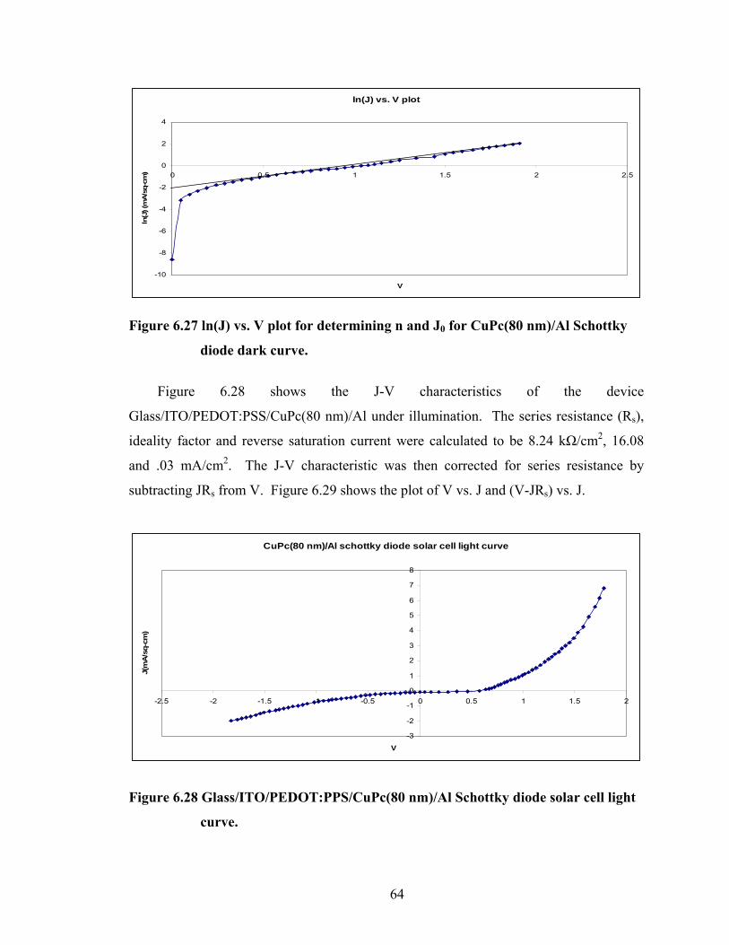
64
ln(J) vs. V plot
-10
-8
-6
-4
-2
0
2
4
0 0.5 1 1.5 2 2.5
V
ln(J
) (m
A/s
q-cm
)
Figure 6.27 ln(J) vs. V plot for determining n and J0 for CuPc(80 nm)/Al Schottky
diode dark curve.
Figure 6.28 shows the J-V characteristics of the device
Glass/ITO/PEDOT:PSS/CuPc(80 nm)/Al under illumination. The series resistance (Rs),
ideality factor and reverse saturation current were calculated to be 8.24 kΩ/cm2, 16.08
and .03 mA/cm2. The J-V characteristic was then corrected for series resistance by
subtracting JRs from V. Figure 6.29 shows the plot of V vs. J and (V-JRs) vs. J.
CuPc(80 nm)/Al schottky diode solar cell light curve
-3
-2
-1
0
1
2
3
4
5
6
7
8
-2.5 -2 -1.5 -1 -0.5 0 0.5 1 1.5 2
V
J(m
A/sq
-cm
)
Figure 6.28 Glass/ITO/PEDOT:PPS/CuPc(80 nm)/Al Schottky diode solar cell light
curve.
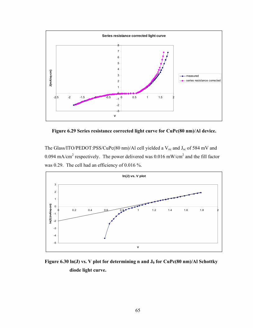
65
Series resistance corrected light curve
-3
-2
-1
0
1
2
3
4
5
6
7
8
-2.5 -2 -1.5 -1 -0.5 0 0.5 1 1.5 2
V
J(m
A/sq
-cm
)
measuredseries resistance corrected
Figure 6.29 Series resistance corrected light curve for CuPc(80 nm)/Al device.
The Glass/ITO/PEDOT:PSS/CuPc(80 nm)/Al cell yielded a Voc and Jsc of 584 mV and
0.094 mA/cm2 respectively. The power delivered was 0.016 mW/cm2 and the fill factor
was 0.29. The cell had an efficiency of 0.016 %.
ln(J) vs. V plot
-5
-4
-3
-2
-1
0
1
2
3
0 0.2 0.4 0.6 0.8 1 1.2 1.4 1.6 1.8 2
V
ln(J
) (m
A/sq
-cm
)
Figure 6.30 ln(J) vs. V plot for determining n and J0 for CuPc(80 nm)/Al Schottky
diode light curve.

66
6.6.4 J-V characteristics of CuPc(100 nm)/Al device
Figure 6.31 shows the J-V characteristics of the device
Glass/ITO/PEDOT:PSS/CuPc (100 nm)/Al under dark conditions. The series resistance
(Rs) of the curve in Figure 6.31 was calculated to be 8.31 kΩ/cm2. The J-V characteristic
was then corrected for series resistance by subtracting JRs from V. Figure 6.32 shows the
plot of V vs. J and (V-JRs) vs. J.
CuPc(100 nm)/Al schottky diode solar cell dark curve
-4
-2
0
2
4
6
8
10
-2 -1.5 -1 -0.5 0 0.5 1 1.5 2 2.5
V
J(m
A/s
q-cm
)
Figure 6.31 Glass/ITO/PEDOT:PPS/CuPc(100 nm)/Al Schottky diode solar cell
dark curve.
Series resistance corrected dark curve
-4
-2
0
2
4
6
8
10
-2 -1.5 -1 -0.5 0 0.5 1 1.5 2 2.5
V
J(m
A/s
q-cm
)
measuredseries resistance corrected dark curve
Figure 6.32 Series resistance corrected dark curve for CuPc(100 nm)/Al device.
67
Figure 6.33 shows the plot of ln(J) vs. V from which the value of Jo was calculated to
be 0.149 mA/cm2. The diode ideality factor n was calculated to be 17.78.
ln(J) vs. V plot
-7
-6
-5
-4
-3
-2
-1
0
1
2
3
0 0.5 1 1.5 2 2.5
V
ln(J
) (m
A/sq
-cm
)
Figure 6.33 ln(J) vs. V plot for determining n and J0 for CuPc(100 nm)/Al Schottky
diode dark curve.
Figure 6.34 shows the J-V characteristics of the device
Glass/ITO/PEDOT:PSS/CuPc (100 nm)/Al under illumination. The series resistance
(Rs), ideality factor and reverse saturation current were calculated to be 8.57 kΩ/cm2,
17.62 and .139 mA/cm2 respectively. The J-V characteristic was then corrected for series
resistance by subtracting JRs from V. Figure 6.35 shows the plot of V vs. J and (V-JRs)
vs. J.
68
CuPc(100 nm)/Al schottky diode solar cell light curve
-3
-2
-1
0
1
2
3
4
5
6
7
8
-2 -1.5 -1 -0.5 0 0.5 1 1.5 2
V
J(m
A/s
q-cm
)
Figure 6.34 Glass/ITO/PEDOT:PPS/CuPc(100 nm)/Al Schottky diode solar cell light
curve.
Series resistance corrected light curve
-3
-2
-1
0
1
2
3
4
5
6
7
8
-2 -1.5 -1 -0.5 0 0.5 1 1.5 2
V
J(m
A/sq
-cm
)
measuredseries resistance corrected
Figure 6.35 Series resistance corrected light curve for CuPc(100 nm)/Al device.
The Glass/ITO/PEDOT:PSS/CuPc(100 nm)/Al cell yielded a Voc and Jsc of 770 mV
and 0.114 mA/cm2. The power delivered was 0.027 mW/cm2 and the fill factor was 0.31.
The cell had an efficiency of 0.027 %.
69
ln(J) vs. V plot
-2.5
-2
-1.5
-1
-0.5
0
0.5
1
1.5
2
2.5
0 0.2 0.4 0.6 0.8 1 1.2 1.4 1.6 1.8 2
V
ln(J
) (m
A/s
q-cm
)
Figure 6.36 ln(J) vs. V plot for determining n and J0 for CuPc(100 nm)/Al Schottky
diode light curve.
6.6.5 J-V characteristics of the CuPc (120 nm)/Al device Figure 6.37 shows the J-V characteristics of the device
Glass/ITO/PEDOT:PSS/CuPc (120 nm)/Al under dark conditions. The series resistance
(Rs) of the curve in Figure 6.37 was calculated to be 9.32 kΩ/cm2. The J-V characteristic
was then corrected for series resistance by subtracting JRs from V. Figure 6.38 shows the
plot of V vs. J and (V-JRs) vs. J.
70
CuPc(120 nm)/Al schottky diode solar cell dark curve
-4
-2
0
2
4
6
8
10
-2 -1.5 -1 -0.5 0 0.5 1 1.5 2 2.5
V
J(m
A/sq
-cm
)
Figure 6.37 Glass/ITO/PEDOT:PPS/CuPc(120 nm)/Al Schottky diode solar cell
dark curve.
Series resistance corrected dark curve
-4
-2
0
2
4
6
8
10
-2 -1.5 -1 -0.5 0 0.5 1 1.5 2 2.5
V
J(m
A/sq
-cm
)
measuredseries resistance corrected
Figure 6.38 Series resistance corrected dark curve for CuPc (120 nm)/Al device.
Figure 6.39 shows the plot of ln(J) vs. V from which the value of Jo was calculated to
be 0.142 mA/cm2. The diode ideality factor n was calculated to be 15.95.
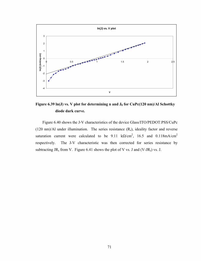
71
ln(J) vs. V plot
-4
-3
-2
-1
0
1
2
3
0 0.5 1 1.5 2 2.5
V
ln(J
) (m
A/s
q-cm
)
Figure 6.39 ln(J) vs. V plot for determining n and J0 for CuPc(120 nm)/Al Schottky
diode dark curve.
Figure 6.40 shows the J-V characteristics of the device Glass/ITO/PEDOT:PSS/CuPc
(120 nm)/Al under illumination. The series resistance (Rs), ideality factor and reverse
saturation current were calculated to be 9.11 kΩ/cm2, 16.5 and 0.118mA/cm2
respectively. The J-V characteristic was then corrected for series resistance by
subtracting JRs from V. Figure 6.41 shows the plot of V vs. J and (V-JRs) vs. J.
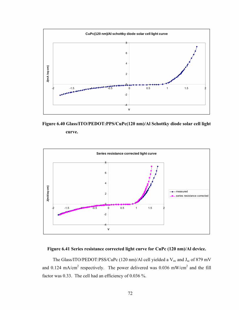
72
CuPc(120 nm)/Al schottky diode solar cell light curve
-4
-2
0
2
4
6
8
-2 -1.5 -1 -0.5 0 0.5 1 1.5 2
V
J(m
A /s
q-cm
)
Figure 6.40 Glass/ITO/PEDOT:PPS/CuPc(120 nm)/Al Schottky diode solar cell light
curve.
Series resistance corrected light curve
-4
-2
0
2
4
6
8
-2 -1.5 -1 -0.5 0 0.5 1 1.5 2
V
J(m
A/sq
-cm
)
measuredseries resistance corrected
Figure 6.41 Series resistance corrected light curve for CuPc (120 nm)/Al device. The Glass/ITO/PEDOT:PSS/CuPc (120 nm)/Al cell yielded a Voc and Jsc of 879 mV
and 0.124 mA/cm2 respectively. The power delivered was 0.036 mW/cm2 and the fill
factor was 0.33. The cell had an efficiency of 0.036 %.

73
ln(J) vs. V plot
-5
-4
-3
-2
-1
0
1
2
3
0 0.2 0.4 0.6 0.8 1 1.2 1.4 1.6 1.8 2
V
ln(J
) (m
A/s
q-cm
)
Figure 6.42 ln(J) vs. V plot for determining n and J0 for CuPc(120 nm)/Al Schottky
diode light curve.
6.6.6 J-V characteristics of the CuPc(140 nm)/Al device
Figure 6.43 shows the J-V characteristics of the device
Glass/ITO/PEDOT:PSS/CuPc (140 nm)/Al under dark conditions. The series resistance
(Rs) of the curve in Figure 6.38 was calculated to be 9.41 kΩ/cm2. The J-V characteristic
was then corrected for series resistance by subtracting JRs from V. Figure 6.44 shows the
plot of V vs. J and (V-JRs) vs. J.
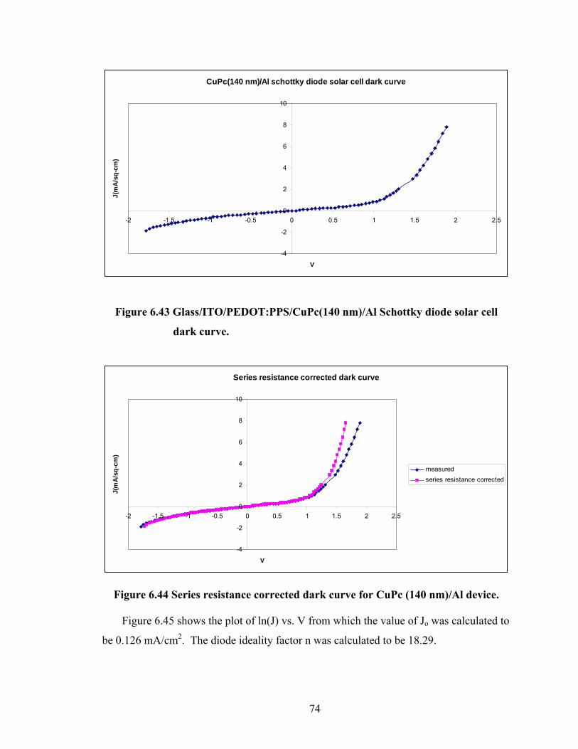
74
CuPc(140 nm)/Al schottky diode solar cell dark curve
-4
-2
0
2
4
6
8
10
-2 -1.5 -1 -0.5 0 0.5 1 1.5 2 2.5
V
J(m
A/sq
-cm
)
Figure 6.43 Glass/ITO/PEDOT:PPS/CuPc(140 nm)/Al Schottky diode solar cell
dark curve.
Series resistance corrected dark curve
-4
-2
0
2
4
6
8
10
-2 -1.5 -1 -0.5 0 0.5 1 1.5 2 2.5
V
J(m
A/sq
-cm
)
measuredseries resistance corrected
Figure 6.44 Series resistance corrected dark curve for CuPc (140 nm)/Al device. Figure 6.45 shows the plot of ln(J) vs. V from which the value of Jo was calculated to
be 0.126 mA/cm2. The diode ideality factor n was calculated to be 18.29.
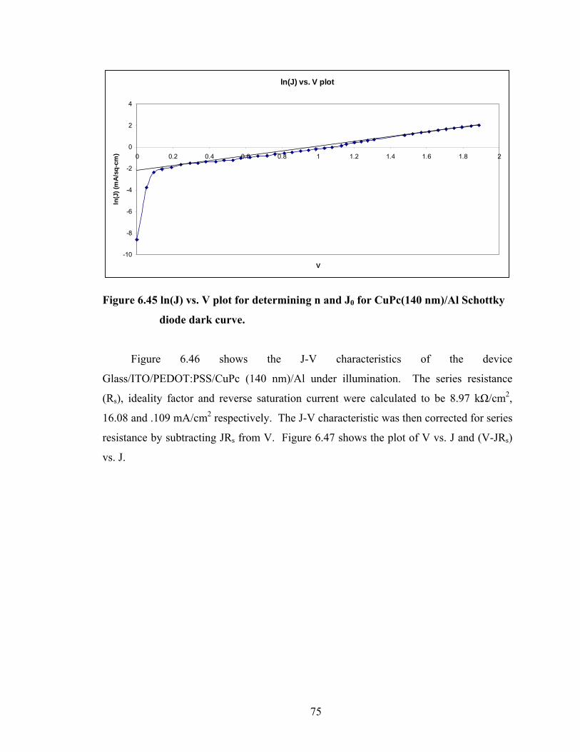
75
ln(J) vs. V plot
-10
-8
-6
-4
-2
0
2
4
0 0.2 0.4 0.6 0.8 1 1.2 1.4 1.6 1.8 2
V
ln(J
) (m
A/s
q-cm
)
Figure 6.45 ln(J) vs. V plot for determining n and J0 for CuPc(140 nm)/Al Schottky
diode dark curve.
Figure 6.46 shows the J-V characteristics of the device
Glass/ITO/PEDOT:PSS/CuPc (140 nm)/Al under illumination. The series resistance
(Rs), ideality factor and reverse saturation current were calculated to be 8.97 kΩ/cm2,
16.08 and .109 mA/cm2 respectively. The J-V characteristic was then corrected for series
resistance by subtracting JRs from V. Figure 6.47 shows the plot of V vs. J and (V-JRs)
vs. J.
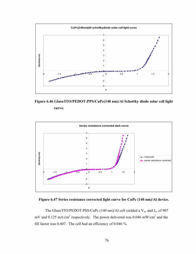
76
CuPc(140nm)/Al schottkydiode solar cell light curve
-3
-2
-1
0
1
2
3
4
5
6
7
-2 -1.5 -1 -0.5 0 0.5 1 1.5 2
V
J(m
A/sq
-cm
)
Figure 6.46 Glass/ITO/PEDOT:PPS/CuPc(140 nm)/Al Schottky diode solar cell light
curve.
Series resistance corrected dark curve
-3
-2
-1
0
1
2
3
4
5
6
7
-2 -1.5 -1 -0.5 0 0.5 1 1.5 2
V
J(m
A/sq
-cm
)
measuredseries resistance corrected
Figure 6.47 Series resistance corrected light curve for CuPc (140 nm)/Al device.
The Glass/ITO/PEDOT:PSS/CuPc (140 nm)/Al cell yielded a Voc and Jsc of 907
mV and 0.125 mA/cm2 respectively. The power delivered was 0.046 mW/cm2 and the
fill factor was 0.407. The cell had an efficiency of 0.046 %.
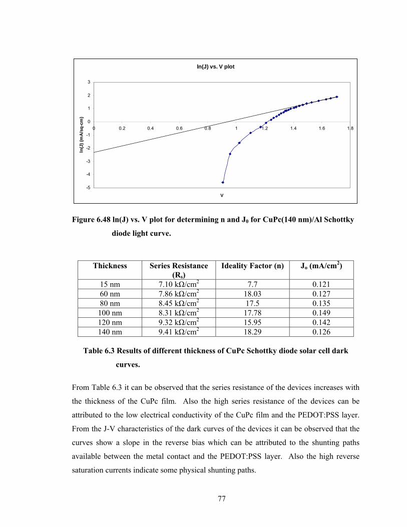
77
ln(J) vs. V plot
-5
-4
-3
-2
-1
0
1
2
3
0 0.2 0.4 0.6 0.8 1 1.2 1.4 1.6 1.8
V
ln(J
) (m
A/s
q-cm
)
Figure 6.48 ln(J) vs. V plot for determining n and J0 for CuPc(140 nm)/Al Schottky
diode light curve.
Thickness Series Resistance (Rs)
Ideality Factor (n) Jo (mA/cm2)
15 nm 7.10 kΩ/cm2 7.7 0.121 60 nm 7.86 kΩ/cm2 18.03 0.127 80 nm 8.45 kΩ/cm2 17.5 0.135 100 nm 8.31 kΩ/cm2 17.78 0.149 120 nm 9.32 kΩ/cm2 15.95 0.142 140 nm 9.41 kΩ/cm2 18.29 0.126
Table 6.3 Results of different thickness of CuPc Schottky diode solar cell dark
curves.
From Table 6.3 it can be observed that the series resistance of the devices increases with
the thickness of the CuPc film. Also the high series resistance of the devices can be
attributed to the low electrical conductivity of the CuPc film and the PEDOT:PSS layer.
From the J-V characteristics of the dark curves of the devices it can be observed that the
curves show a slope in the reverse bias which can be attributed to the shunting paths
available between the metal contact and the PEDOT:PSS layer. Also the high reverse
saturation currents indicate some physical shunting paths.
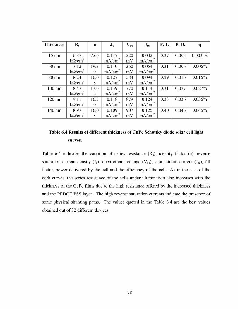
78
Thickness Rs n Jo Voc Jsc
F. F. P. D. η
15 nm 6.87 kΩ/cm2
7.66 0.147 mA/cm2
220 mV
0.042 mA/cm2
0.37 0.003 0.003 %
60 nm 7.12 kΩ/cm2
19.30
0.110 mA/cm2
360 mV
0.054 mA/cm2
0.31 0.006 0.006%
80 nm 8.24 kΩ/cm2
16.08
0.127 mA/cm2
584 mV
0.094 mA/cm2
0.29 0.016 0.016%
100 nm 8.57 kΩ/cm2
17.62
0.139 mA/cm2
770 mV
0.114 mA/cm2
0.31 0.027 0.027%
120 nm 9.11 kΩ/cm2
16.50
0.118 mA/cm2
879 mV
0.124 mA/cm2
0.33 0.036 0.036%
140 nm 8.97 kΩ/cm2
16.08
0.109 mA/cm2
907 mV
0.125 mA/cm2
0.40 0.046 0.046%
Table 6.4 Results of different thickness of CuPc Schottky diode solar cell light
curves.
Table 6.4 indicates the variation of series resistance (Rs), ideality factor (n), reverse
saturation current density (Jo), open circuit voltage (Voc), short circuit current (Jsc), fill
factor, power delivered by the cell and the efficiency of the cell. As in the case of the
dark curves, the series resistance of the cells under illumination also increases with the
thickness of the CuPc films due to the high resistance offered by the increased thickness
and the PEDOT:PSS layer. The high reverse saturation currents indicate the presence of
some physical shunting paths. The values quoted in the Table 6.4 are the best values
obtained out of 32 different devices.
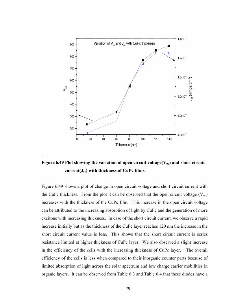
79
.
0 20 40 60 80 100 120 140
200
300
400
500
600
700
800
900
Voc
Thickness (nm)
4.0x10⁻⁵
6.0x10⁻⁵
8.0x10⁻⁵
1.0x10⁻⁴
1.2x10⁻⁴
1.4x10⁻⁴
Variation of Voc and Jsc with CuPc thickness
Jsc
(am
ps/c
m2 )
Figure 6.49 Plot showing the variation of open circuit voltage(Voc) and short circuit
current(Jsc) with thickness of CuPc films.
Figure 6.49 shows a plot of change in open circuit voltage and short circuit current with
the CuPc thickness. From the plot it can be observed that the open circuit voltage (Voc)
increases with the thickness of the CuPc film. This increase in the open circuit voltage
can be attributed to the increasing absorption of light by CuPc and the generation of more
excitons with increasing thickness. In case of the short circuit current, we observe a rapid
increase initially but as the thickness of the CuPc layer reaches 120 nm the increase in the
short circuit current value is less. This shows that the short circuit current is series
resistance limited at higher thickness of CuPc layer. We also observed a slight increase
in the efficiency of the cells with the increasing thickness of CuPc layer. The overall
efficiency of the cells is less when compared to their inorganic counter parts because of
limited absorption of light across the solar spectrum and low charge carrier mobilities in
organic layers. It can be observed from Table 6.3 and Table 6.4 that these diodes have a
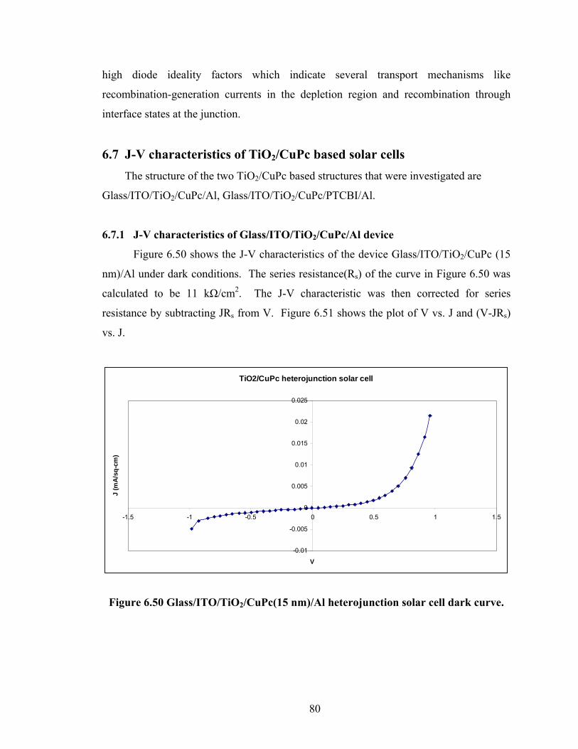
80
high diode ideality factors which indicate several transport mechanisms like
recombination-generation currents in the depletion region and recombination through
interface states at the junction.
6.7 J-V characteristics of TiO2/CuPc based solar cells The structure of the two TiO2/CuPc based structures that were investigated are
Glass/ITO/TiO2/CuPc/Al, Glass/ITO/TiO2/CuPc/PTCBI/Al.
6.7.1 J-V characteristics of Glass/ITO/TiO2/CuPc/Al device
Figure 6.50 shows the J-V characteristics of the device Glass/ITO/TiO2/CuPc (15
nm)/Al under dark conditions. The series resistance(Rs) of the curve in Figure 6.50 was
calculated to be 11 kΩ/cm2. The J-V characteristic was then corrected for series
resistance by subtracting JRs from V. Figure 6.51 shows the plot of V vs. J and (V-JRs)
vs. J.
TiO2/CuPc heterojunction solar cell
-0.01
-0.005
0
0.005
0.01
0.015
0.02
0.025
-1.5 -1 -0.5 0 0.5 1 1.5
V
J (m
A/s
q-cm
)
Figure 6.50 Glass/ITO/TiO2/CuPc(15 nm)/Al heterojunction solar cell dark curve.
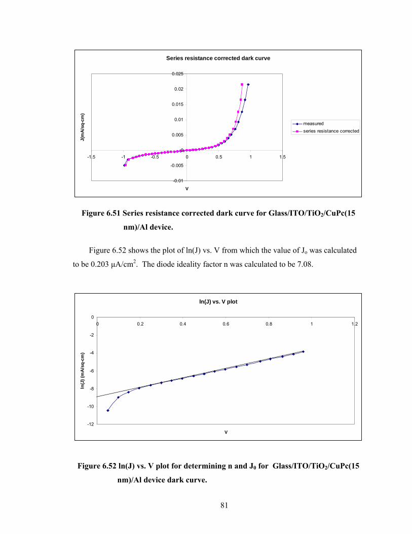
81
Series resistance corrected dark curve
-0.01
-0.005
0
0.005
0.01
0.015
0.02
0.025
-1.5 -1 -0.5 0 0.5 1 1.5
V
J(m
A/sq
-cm
)
measuredseries resistance corrected
Figure 6.51 Series resistance corrected dark curve for Glass/ITO/TiO2/CuPc(15
nm)/Al device.
Figure 6.52 shows the plot of ln(J) vs. V from which the value of Jo was calculated
to be 0.203 µA/cm2. The diode ideality factor n was calculated to be 7.08.
ln(J) vs. V plot
-12
-10
-8
-6
-4
-2
00 0.2 0.4 0.6 0.8 1 1.2
V
ln(J
) (m
A/s
q-cm
)
Figure 6.52 ln(J) vs. V plot for determining n and J0 for Glass/ITO/TiO2/CuPc(15
nm)/Al device dark curve.
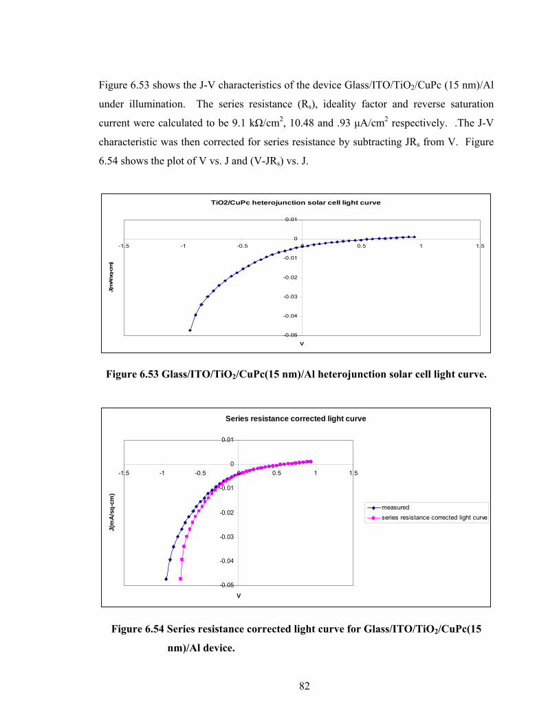
82
Figure 6.53 shows the J-V characteristics of the device Glass/ITO/TiO2/CuPc (15 nm)/Al
under illumination. The series resistance (Rs), ideality factor and reverse saturation
current were calculated to be 9.1 kΩ/cm2, 10.48 and .93 µA/cm2 respectively. .The J-V
characteristic was then corrected for series resistance by subtracting JRs from V. Figure
6.54 shows the plot of V vs. J and (V-JRs) vs. J.
TiO2/CuPc heterojunction solar cell light curve
-0.05
-0.04
-0.03
-0.02
-0.01
0
0.01
-1.5 -1 -0.5 0 0.5 1 1.5
V
J(m
A/sq
-cm
)
Figure 6.53 Glass/ITO/TiO2/CuPc(15 nm)/Al heterojunction solar cell light curve.
Series resistance corrected light curve
-0.05
-0.04
-0.03
-0.02
-0.01
0
0.01
-1.5 -1 -0.5 0 0.5 1 1.5
V
J(m
A/sq
-cm
)
measuredseries resistance corrected light curve
Figure 6.54 Series resistance corrected light curve for Glass/ITO/TiO2/CuPc(15
nm)/Al device.
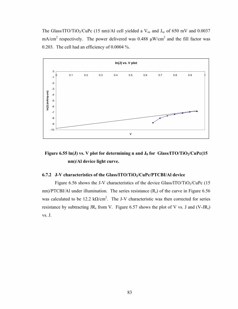
83
The Glass/ITO/TiO2/CuPc (15 nm)/Al cell yielded a Voc and Jsc of 650 mV and 0.0037
mA/cm2 respectively. The power delivered was 0.488 µW/cm2 and the fill factor was
0.203. The cell had an efficiency of 0.0004 %.
ln(J) vs. V plot
-10
-9
-8
-7
-6
-5
-4
-3
-2
-1
00 0.1 0.2 0.3 0.4 0.5 0.6 0.7 0.8 0.9 1
V
ln(J
) (m
A/sq
-cm
)
Figure 6.55 ln(J) vs. V plot for determining n and J0 for Glass/ITO/TiO2/CuPc(15
nm)/Al device light curve.
6.7.2 J-V characteristics of the Glass/ITO/TiO2/CuPc/PTCBI/Al device
Figure 6.56 shows the J-V characteristics of the device Glass/ITO/TiO2/CuPc (15
nm)/PTCBI/Al under illumination. The series resistance (Rs) of the curve in Figure 6.56
was calculated to be 12.2 kΩ/cm2. The J-V characteristic was then corrected for series
resistance by subtracting JRs from V. Figure 6.57 shows the plot of V vs. J and (V-JRs)
vs. J.
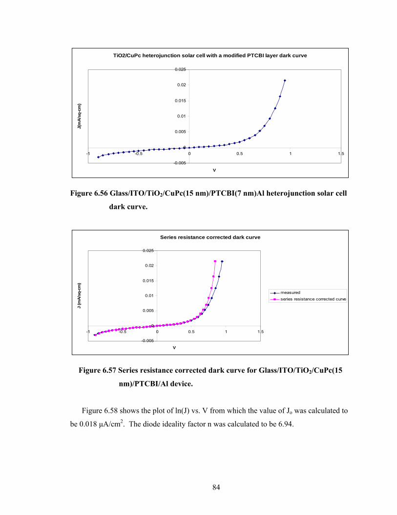
84
TiO2/CuPc heterojunction solar cell with a modified PTCBI layer dark curve
-0.005
0
0.005
0.01
0.015
0.02
0.025
-1 -0.5 0 0.5 1 1.5
V
J(m
A/sq
-cm
)
Figure 6.56 Glass/ITO/TiO2/CuPc(15 nm)/PTCBI(7 nm)Al heterojunction solar cell
dark curve.
Series resistance corrected dark curve
-0.005
0
0.005
0.01
0.015
0.02
0.025
-1 -0.5 0 0.5 1 1.5
V
J (m
A/sq
-cm
)
measuredseries resistance corrected curve
Figure 6.57 Series resistance corrected dark curve for Glass/ITO/TiO2/CuPc(15
nm)/PTCBI/Al device.
Figure 6.58 shows the plot of ln(J) vs. V from which the value of Jo was calculated to
be 0.018 µA/cm2. The diode ideality factor n was calculated to be 6.94.
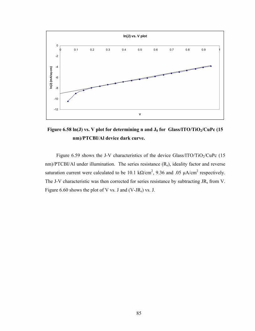
85
ln(J) vs. V plot
-12
-10
-8
-6
-4
-2
00 0.1 0.2 0.3 0.4 0.5 0.6 0.7 0.8 0.9 1
V
ln(J
) (m
A/sq
-cm
)
Figure 6.58 ln(J) vs. V plot for determining n and J0 for Glass/ITO/TiO2/CuPc (15
nm)/PTCBI/Al device dark curve.
Figure 6.59 shows the J-V characteristics of the device Glass/ITO/TiO2/CuPc (15
nm)/PTCBI/Al under illumination. The series resistance (Rs), ideality factor and reverse
saturation current were calculated to be 10.1 kΩ/cm2, 9.36 and .05 µA/cm2 respectively.
The J-V characteristic was then corrected for series resistance by subtracting JRs from V.
Figure 6.60 shows the plot of V vs. J and (V-JRs) vs. J.
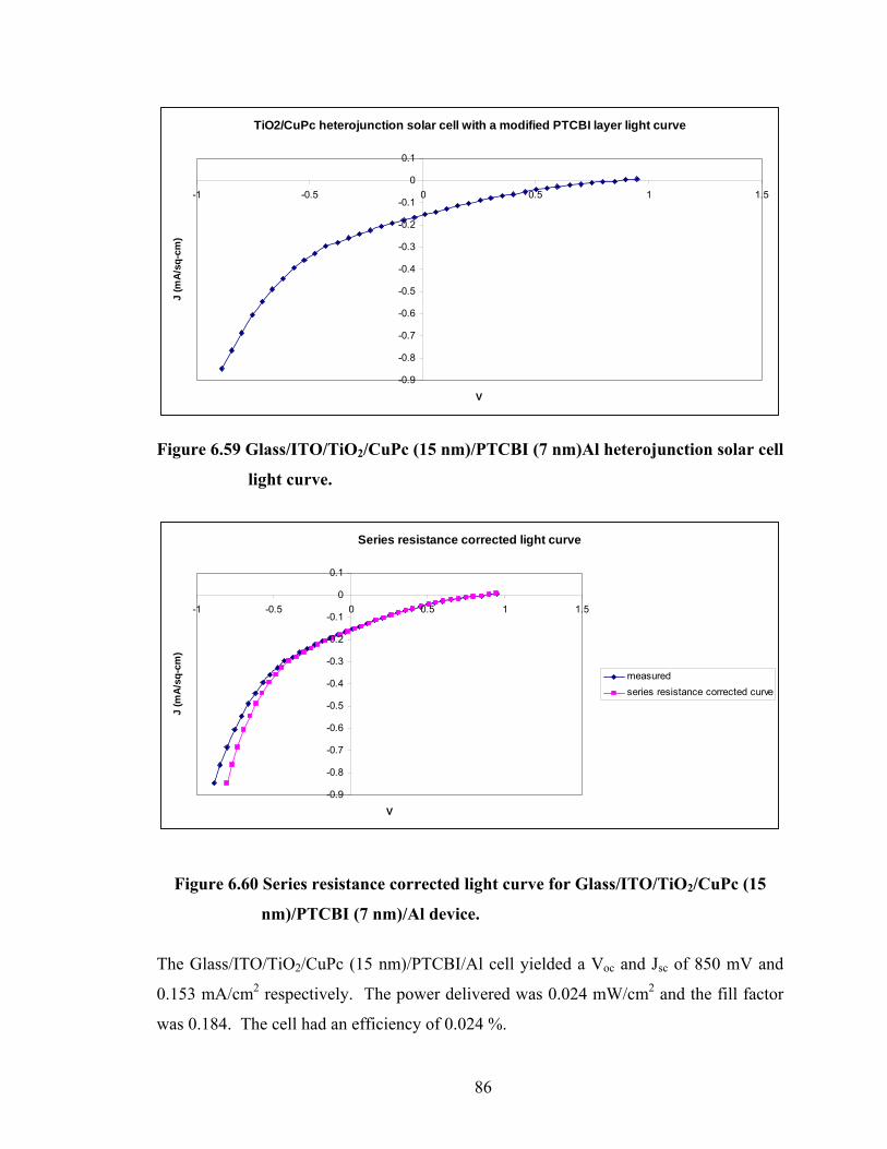
86
TiO2/CuPc heterojunction solar cell with a modified PTCBI layer light curve
-0.9
-0.8
-0.7
-0.6
-0.5
-0.4
-0.3
-0.2
-0.1
0
0.1
-1 -0.5 0 0.5 1 1.5
V
J (m
A/s
q-cm
)
Figure 6.59 Glass/ITO/TiO2/CuPc (15 nm)/PTCBI (7 nm)Al heterojunction solar cell
light curve.
Series resistance corrected light curve
-0.9
-0.8
-0.7
-0.6
-0.5
-0.4
-0.3
-0.2
-0.1
0
0.1
-1 -0.5 0 0.5 1 1.5
V
J (m
A/s
q-cm
)
measuredseries resistance corrected curve
Figure 6.60 Series resistance corrected light curve for Glass/ITO/TiO2/CuPc (15
nm)/PTCBI (7 nm)/Al device.
The Glass/ITO/TiO2/CuPc (15 nm)/PTCBI/Al cell yielded a Voc and Jsc of 850 mV and
0.153 mA/cm2 respectively. The power delivered was 0.024 mW/cm2 and the fill factor
was 0.184. The cell had an efficiency of 0.024 %.
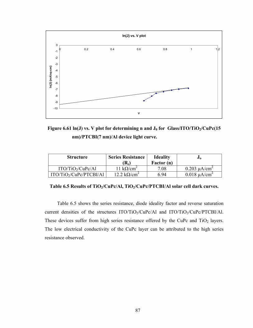
87
ln(J) vs. V plot
-10
-9
-8
-7
-6
-5
-4
-3
-2
-1
00 0.2 0.4 0.6 0.8 1 1.2
V
ln(J
) (m
A/sq
-cm
)
Figure 6.61 ln(J) vs. V plot for determining n and J0 for Glass/ITO/TiO2/CuPc(15
nm)/PTCBI(7 nm)/Al device light curve.
Structure Series Resistance (Rs)
Ideality Factor (n)
Jo
ITO/TiO2/CuPc/Al 11 kΩ/cm2 7.08 0.203 µA/cm2 ITO/TiO2/CuPc/PTCBI/Al 12.2 kΩ/cm2 6.94 0.018 µA/cm2
Table 6.5 Results of TiO2/CuPc/Al, TiO2/CuPc/PTCBI/Al solar cell dark curves.
Table 6.5 shows the series resistance, diode ideality factor and reverse saturation
current densities of the structures ITO/TiO2/CuPc/Al and ITO/TiO2/CuPc/PTCBI/Al.
These devices suffer from high series resistance offered by the CuPc and TiO2 layers.
The low electrical conductivity of the CuPc layer can be attributed to the high series
resistance observed.

88
Structure Rs n Jo Voc Jsc
F. F. P. D. η
ITO/TiO2/CuPc/Al
9 kΩ/cm2
10.4 0.93 µA/cm2
650 mV
0.0037 mA/cm2
0.20 0.488 µW/cm2
0.0004%
ITO/TiO2/CuPc/PTC
BI/Al
10.1 kΩ/cm2
9.36 0.05 µA/cm2
850 mV
0.153 mA/cm2
0.18 0.024 mW/cm2
0.024%
Table 6.6 Results of TiO2/CuPc heterojunction and TiO2/CuPc heterojunction with
a modified PTCBI layer light curves.
Table 6.6 shows the cell parameters for ITO/TiO2/CuPc/Al and ITO/TiO2
/CuPc/PTCBI/Al structures. As in the case of the dark curves the light curves also suffer
from high series resistance offered by the CuPc and TiO2 layers. The low value of
reverse saturation current in case of the ITO/TiO2/CuPc/PTCBI/Al structure when
compared to the ITO/TiO2/CuPc/Al structure suggests that the PTCBI layer is protecting
the CuPc layer from being damaged by the high energy aluminium atoms. As
hypothesized by V.P. Singh et al. [29] part of the PTCBI layer may actually be used up
by aluminium in the formation of aluminium oxide (Al2O3) which forms a thin insulating
layer and thereby protecting the CuPc from being damaged. Apart from forming a
heterojunction with CuPc, the presence of pores in the TiO2 layer helps in the scattering
of light resulting in the increase of optical path and thereby increasing the open circuit
voltage of the device. A considerable increase in the short circuit current could not be
observed because of the high series resistance offered by the CuPc layer. The
ITO/TiO2/CuPc/PTCBI/Al structure shows a better photovoltaic behavior because of the
protection of CuPc layer by the thin PTCBI layer. The cells suffer from low efficiencies
due to various factors like high series resistance, low carrier mobilities in the organic
layer and rapid degradation of organic films when exposed to air.
89
Chapter 7. Discussion 7.1 Material characterization of C60
C60 is a molecule that consists of 60 carbon atoms in the form of a sphere. This
sphere is made up of 12 hexagons and 12 pentagons with a carbon atom on each corner.
C60 is a well known n-type organic semiconductor used in the fabrication of solar cells
and OLEDs. Figure 4.1 shows the SEM image of the C60 film at high magnification and
Figure 4.2 shows the SEM image of C60 at low magnification. The average particle size
of C60 deposited on an ITO coated glass substrate was 30 nm. The low magnification
image shows that the deposited film was uniform.
Figure 4.3 shows the X-ray diffraction pattern of the C60 film. The C60 film that was
thermally evaporated showed peaks at 2θ positions of 10.10, 220 and 340 which
correspond to 111, 222 and 333 planes respectively. C60 films did not show any preferred
orientation which can be attributed to lattice mismatch between C60 and ITO. The peaks
produced by C60 films were compared to the ones that were obtained by Z. Dai et al. [30].
The peaks produced at 2θ positions of 230, 300, 310, 350, 370, 450, 510 and 600 are
produced by ITO.
7.2 Optical characterization of C60 The Optical absorption plot of a material gives a fair idea of the absorption
characteristics of the material in the visible spectrum, which is an important characteristic
of a good photovoltaic material. A good photovoltaic material should have broad peaks
of absorption in the visible spectrum of light to utilize most of the light passing through it
to generate carriers. Absorption vs. wavelength plot of C60 film of thickness 40 nm is
shown in Figure 5.1. The absorption plot shows peaks at wavelengths of 350 nm and at
450 nm. The absorption plot showed peaks at the same positions as obtained by Tetsuya
Taima et al. [4]. C60 is a symmetric molecule and hence the transition between the
HOMO and LUMO levels is forbidden, which can be attributed to the lack of a strong
absorption band in the visible region of the absorption spectrum of C60 [4].
90
7.3 Electrical characterization of C60 Schottky diode solar cells The ITO/C60(40 nm)/LiF/Al structure showed a series resistance of 78.06 Ω/cm2
and the ITO/PEDOT:PSS/C60(60 nm)/LiF/Al structure showed a series resistance of 0.75
kΩ/cm2 in case of the dark curves. The increase in the value of series resistance from the
ITO/C60 (40 nm)/LiF/Al structure to the ITO/PEDOT:PSS/C60 (60 nm)/LiF/Al structure
can be attributed to low carrier mobilities in the PEDOT:PSS layer. A Lithium Fluoride
(LiF) layer of thickness 1 nm was deposited on the C60 films before the deposition of
aluminium to protect the C60 layer from being damaged by the high energy aluminium
atoms. In the case of both these devices a Schottky barrier is formed between the C60
layer and the aluminium layer since the thickness of LiF layer is 1 nm. The PEDOT:PSS
layer which was used in the ITO/PEDOT:PSS/C60 (60 nm)/LiF/Al structure serves to
make the surface of the ITO smooth and also to reduce the availability of shunting paths
between aluminium and the ITO.
The value of diode ideality factor for dark curves in the case of the ITO/C60 (40
nm)/LiF/Al structure was 5.73 and its value is 13 in case of ITO/PEDOT:PSS/C60 (60
nm)/LiF/Al structure (see Table 6.1). These high diode ideality factors indicate several
transport mechanisms like recombination-generation currents in the depletion region and
recombination through interface states. The high diode ideality factors may also be
attributed to tunneling from band states to localized defect states and band-to-band
tunneling. The value of reverse saturation current for dark curves in the case of the
ITO/C60 (40 nm)/LiF/Al structure was 0.019 mA/cm2 and 0.047 mA/cm2 in the case of
the ITO/PEDOT:PSS/C60 (60 nm)/LiF/Al structure (see Table 6.1). The presence of
physical shunting paths is reasonable considering these high reverse saturation currents
and the fact that the curves have a slope in the third quadrant.
Table 6.2 indicates the variation of different cell parameters in the case of the
ITO/C60 (40 nm)/LiF/Al and the ITO/PEDOT:PSS/C60 (60 nm)/LiF/Al structures. The
increase in series resistance from 40 nm device (63.08 Ω/cm2) to 60 nm device (0.12
kΩ/cm2) was also observed in the case of the light curves. The increase in the value of
open circuit voltage from 190 mV (40 nm device) to 310 mV (60 nm device) without any
increase in the value of short circuit currents (0.49 mA/cm2 for 40 nm device and 0.48
mA/cm2 for 60 nm device) indicates the availability of fewer shunting paths in case of the
91
60 nm device as a result of the inclusion of the PEDOT:PSS layer. An increase in the
efficiency from 0.021% (40 nm device) to 0.028% (60 nm device) was also observed.
Tetsuya Taima et al. [4] have reported an open circuit voltage of 0.046 V and a short
circuit current of 2.77 x 10² mA/cm2 for ITO/C60 (100 nm)/Al structure. The high values
of open circuit voltage observed in C60/Al Schottky diodes fabricated in our lab can be
attributed to the reduction in the thickness of the C60 layer as compared to the devices
fabricated by Tetsuya Taima et al.. The value of short circuit currents can be increased
by sublimating C60 before thermal evaporation since sublimation is known to eliminate
the impurities present in the material.
7.4 Material characterization of CuPc CuPc was used in the fabrication of ITO/PEDOT:PSS/CuPc/Al, ITO/TiO2/CuPc/Al
and ITO/TiO2/CuPc/PTCBI/Al structures. CuPc is a well known p-type organic
semiconductor used in the fabrication of organic solar cells and OLEDs. Figures 4.4 and
4.5 show the SEM images of CuPc at high and low magnifications respectively. It can be
observed from Figure 4.4 that the average particle size of the CuPc film is approximately
30 nm.
Figure 4.6 shows the X-ray diffraction pattern of the CuPc film. The CuPc film
showed a peak at 2θ position of 6.850 which corresponds to 111 plane as observed by
M.M. El-Nahass et al. [31]. The peaks at 2θ position of 230, 300, 310, 350, 370, 450, 510
and 600 are produced by ITO. The fact that the CuPc film showed a single peak at 2θ
position of 6.850 shows that it has a preferred orientation which results in better
transportation of carriers.
7.5 Optical characterization of CuPc The absorption vs. wavelength plots of CuPc films of thickness 15nm, 60 nm, 80
nm, 100 nm, 120 nm and 140 nm are plotted together in Figure 5.15. These plots showed
absorption peaks at wavelengths 350 nm, 620 nm and 700 nm as observed by C.Y.
Kwong et al. [7]. The absorption of these films increased with the thickness of the films
as expected. Figure 5.16 shows the absorption coefficient vs. wavelength plot of the
CuPc films. It can be observed from Figure 5.16 that the absorption coefficients of the
92
CuPc films of thickness 80nm, 100 nm, 120 nm and 140 nm are approximately equal.
The absorption coefficients of CuPc films of thickness 15 nm and 60 nm are less than the
absorption coefficients of films of thickness 80 nm and above. This behavior can be
attributed to the scattering of light, and to reflection in 15 nm and 60 nm films since the
thickness of the films is less compared to the films of thickness 80 nm and above.
7.6 Electrical characterization of CuPc Schottky diode solar cells ITO/PEDOT:PSS/CuPc (x)/Al devices were fabricated and were measured to
calculate the photovoltaic parameters where ‘x’ is the thickness of the CuPc layer and its
values are 15 nm, 60 nm, 80 nm, 100 nm, 120 nm and 140 nm. Table 6.3 shows the
variation of series resistance, ideality factor and reverse saturation current of these
devices measured in the dark. In these devices, the Schottky barrier is formed between
the CuPc layer and aluminium. PEDOT:PSS was used to smooth the surface of ITO.
From Table 6.3 it can be seen that the series resistance increases with increases in the
thickness of the CuPc film. The high values of series resistance in the case of these
devices can be attributed to low carrier mobilities in the CuPc film and PEDOT:PSS
layer. The value of reverse saturation current in these devices is also high indicating the
presence of physical shunting paths available between aluminium and ITO. Also, the
slope of the curves in the third quadrant indicates the presence of physical shunting paths.
The diode ideality factor in these devices were also high indicating that the current
transport in these devices cannot be explained with just the diffusion current dominated
model. The other transport mechanisms like recombination-generation currents in the
depletion region, band-to-band tunneling and recombination through interface states at
the junction may be operative at the interface.
Table 6.4 lists the photovoltaic parameters of the CuPc/Al Schottky diode solar
cells. As in the case of CuPc/Al Schottky diode dark curves the increase in the series
resistance with the thickness of the CuPc layer was also observed in case of the light
curves. An increase in the value of open circuit voltage and short circuit current was
observed with increase in the thickness of the CuPc layer, which can be attributed to the
increased absorption of light with the thickness of the CuPc film as observed in Figure
5.15. Figure 6.49 shows a plot in which the values of Voc and Jsc are plotted against the
93
thickness of the CuPc layer. The values of open circuit voltage does not change much
from 100 nm device to 140 nm device which suggests that the exciton diffusion length of
the CuPc is approximately 120 nm. An exciton diffusion length of 10 to 50 nm for CuPc
was suggested by Fan Yang et al. [32]. It may be possible that the some of the excitons
generated in these Schottky devices are dissociated by the electrostatic field generated by
the difference in work functions of ITO and Aluminium electrodes and hence the exciton
diffusion length may actually be less than 100 nm. The efficiency of the CuPc Schottky
diode solar cells increases with the thickness of the CuPc layer, which can be attributed to
the increase in the open circuit voltage and short circuit current of these devices with the
increase in the thickness of CuPc layer. The low values of efficiencies in case of the
CuPc Schottky diode solar cells can be attributed to low mobility of carriers in CuPc
films.
7.7 Material characterization of TiO2 The TiO2 sol-gel was spin coated on the surface of ITO with the help of a
spincoater at an rpm of 2000. The TiO2 films that were spin coated at higher speeds were
of poor quality in terms of film uniformity. The TiO2 sol-gel was spin coated 4 times on
the substrates and the thickness of the film was found to be approximately 30 nm using
profilometer measurements. ITO/TiO2/CuPc/Al devices with 8 times spincoated TiO2
layers were also fabricated but they did not yield any Voc and Jsc. The motive behind
using the TiO2 layer in these devices was to increase the effective optical path of light by
allowing the light to pass through the pores formed on the annealed TiO2 layer. Figure
4.7 and Figure 4.8 show the high and low magnification images of the TiO2 layer
annealed at a temperature of 300OC. The average particle size of the TiO2 film was
approximately 25 nm. The macropores formed on the TiO2 film were of diameter 300
nm and the density of the pores formed is approximately 0.15 per (µm)2.
7.8 Optical characterization of TiO2 Figure 5.17 and Figure 5.18 show the absorption vs. wavelength and absorption
coefficient vs. wavelength plots of the TiO2 sol-gel that was spincoated on ITO
substrates. The approximate thickness of the spincoated TiO2 layer was 30 nm. The
94
TiO2 film had absorption peaks at wavelengths of 500 nm and 300 nm. The low
absorption peaks of the TiO2 film indicate that the film is a good window layer which can
be used in solar cells.
7.9 Electrical characterization of ITO/TiO2/CuPc/Al and
ITO/TiO2/CuPc/PTCBI/Al solar cells ITO/TiO2/CuPc (15 nm)/Al solar cells were fabricated with the motive of increasing
the effective optical path of light by allowing light to pass through the pores formed in
the annealed TiO2 layer. In this device a heterojunction is formed at the interface of the
CuPc (15 nm) layer and the spincoated TiO2 layer. Also, a Schottky barrier is formed at
the interface of the CuPc layer and the Aluminium layer. The value of open circuit
voltage observed in case of the CuPc (15 nm)/Al Schottky diode solar cell was 430 mV
(see Table 6.6) less than the value of open circuit voltage observed in TiO2/CuPc(15
nm)/Al structure indicating the dominance of the TiO2/CuPc heterojunction over the
CuPc(15 nm)/Al Schottky barrier. The density of the pores formed on the surface of
annealed TiO2 was low (0.15 per (µm)2), hence the effective optical path of light could
not be increased significantly. Table 6.5 shows the values of series resistance, diode
ideality factor and reverse saturation current obtained from the J-V characteristics of the
dark curve of ITO/TiO2/CuPc (15 nm)/Al structure. The value of series resistance was
found to be 11 kΩ/cm2 indicating the high series resistance offered by the CuPc and TiO2
layers. The value of diode ideality factor was found to be 7.08 which is quite high
indicating the presence of several transport mechanisms like generation-recombination
currents and recombination through interface states. The value of reverse saturation
currents is less when compared to the ITO/PEDOT:PSS/CuPc (x)/Al structures indicating
less number of shunting paths available in the ITO/TiO2/CuPc (15 nm)/Al structure.
Table 6.6 shows the values of photovoltaic parameters for the ITO/TiO2/CuPc (15
nm)/Al structure. The value of open circuit voltage was 650 mV and the value of short
circuit current was 0.0037 mA/cm2. A.K. Ray et al. [8] have reported a ITO/TiO2/CuPc
(460 nm)/Au solar cell with an open circuit voltage of 0.024 V and a short circuit current
of 0.012 mA/cm2. The higher value of open circuit voltage observed in case of the
TiO2/CuPc/Al device fabricated in our lab can be attributed to the reduction in the
95
thickness of CuPc layer from 460 nm (used by A.K Ray et al. [8]) to 15 nm which
eliminates the recombination of excitons during their movement from the junction
towards the metal contacts.
Table 6.5 shows the series resistance, diode ideality factor and reverse saturation
current values of the ITO/TiO2/CuPc (15 nm)/PTCBI/Al structure. PTCBI, a well known
n-type organic semiconductor was used both to form a heterojuntion with the CuPc layer
and also to protect the CuPc layer from high energy Aluminium atoms. In this device a
heterojunction is formed at the interface of TiO2 and CuPc layers and also at the interface
of CuPc and PTCBI layers. The increase in the value of open circuit voltage from
ITO/TiO2/CuPc (15 nm)/Al structure to ITO/TiO2/CuPc (15 nm)/PTCBI/Al structure
suggests that the CuPc/PTCBI junction is the dominant junction in the ITO/TiO2/CuPc
(15 nm)/PTCBI/Al structure. The value of series resistance was calculated to be 12.2
kΩ/cm2, which can be attributed to the low mobility of carriers in CuPc and PTCBI
layers. The value of diode ideality factor was calculated to be 6.94 indicating the
presence of several transport mechanisms like generation-recombination currents,
recombination through interface states and band-to-band tunneling. The low value of
reverse saturation current (0.018 µA/cm2) shows the presence of less number of shunting
paths available in the device.
Table 6.6 shows the photovoltaic parameters of the ITO/TiO2/CuPc (15
nm)/PTCBI/Al structure. An increase in the values of open circuit voltage and short
circuit current which can be seen from Table 6.6 was observed from ITO/TiO2/CuPc (15
nm)/Al structure to ITO/TiO2/CuPc (15 nm)/PTCBI/Al structure which can be attributed
to the addition of a more dominant CuPc (15 nm)/PTCBI junction to the TiO2/CuPc (15
nm) junction. These cells suffer from low efficiencies due to various factors like low
carrier mobilities in the organic layers and rapid degradation of the organic films when
exposed to air.
96
Chapter 8. Conclusions C60/Al Schottky diode solar cells were fabricated on ITO coated glass slides. The 40
nm thick C60 device yielded a open-circuit voltage of 190 mV and a short-circuit current
density of 0.49 mA/cm2. LiF was used to improve the fill factor of the devices and also
to shield the C60 from high energy Aluminium atoms. The 60 nm thick C60 device
yielded an open circuit voltage of 310 mV and a short circuit current of 0.48 mA/cm2.
We can observe an increase in the open circuit voltage of the 60 nm device when
compared to the 40 nm device. The increase in the open circuit voltage can be attributed
to the increase in the absorption of the film. The low mobilties of charge carriers in the
organic films and also the PEDOT:PSS layer resulted in high series resistance and low
current values.
Also, CuPc/Al Schottky diode solar cells were fabricated on ITO coated glass
substrates. We observed an increase in open circuit voltage from 220 mV in the case of
the 15 nm thick device upto 907 mV in the case of the 140 nm thick device. The increase
in the open circuit voltage can be attributed to the increasing absorption of light by CuPc
and generation of more excitons with increasing thickness. In case of the short circuit
current, we observe a rapid increase initially from 0.042 mA/cm2 (15 nm thick device) to
0.124 mA/cm2 (120 nm thick device) but as the thickness of the CuPc layer reaches 120
nm the increase in the short circuit current is less which can be observed from the short
circuit current for the 140 nm thick device whose value is 0.125 mA/cm2. This shows
that the short circuit current is series resistance limited at higher thickness of the CuPc
layer. We also observed an increase in the efficiency of the cells from 0.003% (15 nm
thick device) to 0.046% (140 nm thick device) with increasing thickness of the CuPc
layer. The overall efficiency of the cells is very small when compared to their inorganic
counterparts because of limited absorption of light across the solar spectrum and low
charge carrier mobilities in organic layers.
Furthermore, TiO2/CuPc/Al and TiO2/CuPc/PTCBI/Al devices were fabricated on
ITO coated glass substrates. The values of open circuit voltage were 650 mV in case of
ITO/TiO2/CuPc/Al structure and 850 mV in case of the ITO/TiO2/CuPc/PTCBI/Al
structure. These values of open circuit voltages were one of the highest ever reported
values for TiO2 based solar cells. The low value of reverse saturation current in case of

97
the ITO/TiO2/CuPc/PTCBI/Al structure whose value is 0.05 µA/cm2 when compared to
the ITO/TiO2/CuPc/Al structure whose value is 0.93 µA/cm2 suggests that the PTCBI
layer is protecting the CuPc layer from being damaged by the Aluminium atoms and
thereby reducing the shunting paths available. The cells suffer from low efficiencies due
to various factors like high series resistance and low carrier mobilities in the organic
layers.
98
Chapter 9. Suggestions to future work The efficiency of the C60 and CuPc Schottky diode solar cells can be greatly
improved by depositing the C60 and CuPc in porous alumina templates and thereby
increasing the scattering of light. Electrodeposition of the organic films instead of
thermal evaporation can be more useful since electrodeposition leads to a better
conformal deposition of the films into the pores. The performance of the TiO2 based
devices can be improved by annealing the TiO2 films at a higher temperature. A study of
lifetime of the organic solar cells can also be very useful in judging the practical usage of
these cells. Organic semiconductors with higher mobilities as opposed to the ones used
in this work can also be very useful for the fabrication of solar cells with higher
efficiencies.
The organic materials used in this work were deposited without being subjected to
any prior purification before deposition. Sublimation of the organic materials is known
to improve their purity and thereby increasing the mobility of carriers. C60, CuPc and
PTCBI can be purified by sublimation before thermal evaporation which can lead to
higher efficiencies. Also, other metal electrodes like silver, gold and platinum can be
used in place of aluminium to increase the value of short circuit currents. Also, the
composition of the chemicals used in the TiO2 sol-gel can be varied to increase the
density of pores and thereby increasing the effective optical path of light.
ITO/TiO2/CuPc/PTCBI/Al device with an open circuit voltage of 850 mV and a short
circuit current density of 0.153 mA/cm2 is the best device to pursue for further work. The
value of efficiency which is 0.024% for the ITO/TiO2/CuPc/PTCBI/Al device, can be
increased by decreasing the value of series resistance. Sublimation of the organic
materials used in the fabrication of the device can lead to lower values of series resistance
and hence higher values of short circuit currents.
99
References 1. V. D. Mihailetchi, P. W. M. Blom, J. C.Hummelen and M. T. Rispens, Journal of
Applied Physics, Vol. 94, Number 10, 2003.
2. C. W. Tang, Applied Physics Letters, 48, 1986.
3. Jenny Nelson, James Kirkpatrick and P. Ravirajan, Physical Review B 69, 035337,
2004.
4. Tetsuya Taima, Masayuki Chikamatsu, Raghu Nath Bera, Yuji Yoshida, Kazuhiro
Saito and Kiyoshi Yase, The Journal of Physical Chemistry, Vol. 108, Number 1,
January 8, 2004.
5. F.T. Reis, D. Mencaraglia, S. Oould Saad, I. Seguy, M.Oukachmih, P.Jolinat,
P.Destruel, Synthetic Metals 138, 2003.
6. H. Ding, M. K .Ram, L. Zheng, C. Nicolini, Journal of Material Science 36 (2001).
7. C.Y. Kwong, A.B.Djurisic, P.C. Chui, L.S.M. Lam, W.K. Chan, Applied Physics
A, Material Science & Processing, 77, 555-560 (2003).
8. A. K. Ray, S.M. Tracey, A.K. Hassan, S.T. Shishiyanu, T.S. Shishiyanu,
Moldavian Journal of The Physical Sciences, N2, 2002.
9. S. M. Sze, Physics of semiconductor devices, 2nd edition, Chapter 5.
10. R. S. Muller, Theodore Cummins, Solid State Electronic Devices, Chapter 2.
11. Ben G. Streetman, Solid State Electronic Devices, Prentice Hall, 3rd edition.
12. Jenny Nelson, Current Opinion in Solid State & Materials Science 6 (2002) 87-95.
13. Brian A. Gregg, Journal of Physical Chemistry B 2003, 107, 4688-4698.
14. D. Meissner, J. Rostalski, Synthetic Materils 121 (2001) 1551-1552.
15. Charles Kittel, Introduction to Solid State Physics, 7th edition, John Wiley and Sons.
16. Thomas Stubinger and Wolfgang Brutting, Journal of Applied Physics, Vol. 90,
Number 7, 2001.
17. Jenny Nelson, The Physics of Solar Cells, Imperial College Press.
18. Brabec, V. Dyakonov, J. Parisi, N. S. Sacricifti, Organic Photovoltaics, Springer
Series.
19. Alan L. Fahrenbruch, Richard H. Bube, Fundamentals of Solar cells, Academic
press, INC.
20. David L. Pulfrey, Photovoltaic Power Generation, Van Nostrand Reinhold

100
Company.
21. W.D. Johnston, Jr., Solar Voltaic Cells, Marcel Dekker, INC.
22. Kasturi Lal Chopra, Suhit Ranjan Das, Thin Film Solar Cells, Plenum Press.
23. Craig A. Grimes and R. Suresh Singh, Journal of Materials Research, 16(6),
2001.
24. R. Suresh Singh, C.A. Grimes and E.C.Dickey, Materials Reasearch Innovation,
5(3-4), 178-184, 2002.
25. Christoph J. Brabec, Sean E. Shaheen, Christoph Winder and N. Serdar Sacricifti,
Applied Physics Letters, Vol. 80, Number 7, 2002.
26. Basics of X-Ray Diffraction, Thermo ARL, ARL Applied Research Laboratories.
http://www.thermo.com/com/cda/home
27. Principles of Scanning Electron Microscopy, Department of Biology, University of
Dayton.
28. Dr. Glagovich, Central Connecticut State University.
http://www.chemistry.ccsu.edu/glagovich/teaching/472/uvvis/measure.html
29. V. P. Singh, R. S. Singh, B. Parthasarathy and A. Aguilera, Applied Physics Letters,
86, 2005.
30. Z. Dai, H. Naramoto, Journal of Physics, 1999.
31. M.M. El-Nahass, F.S. Bahabri, A.A. Al Ghamdi, S.R. Al-Habri, Egypt. J. Sol.
Vol. (25), No. (2), (2002).
32. Fan Yang, Max Shtein and Stephen R. Forrest , Nature Materials 4, 37-41 (2005).
101
Vita Subhash C.C. Vallurupalli was born in Eluru, West Godavari district, Andhra Pradesh,
India on May 14, 1981. He received his Bachelor of Engineering degree in Electronics
and Communication Engineering in 2002 from Osmania University, Hyderabad, India.
He worked as a Research Assistant from 2004-2005 in the Electronic Devices Research
Group at the University of Kentucky, Lexington, Kentucky, U.S.A..
______________________ Subhash C. C. Vallurupalli