Embed Size (px)
Citation preview
MICROELECTRONICS BIOINSTRUMENTATION SYSTEMS
FINAL REPORT
October 1, 1976 to September 30, 1977
Research Grant NGR-36-027-053
fa/0 . >yWen H. Ko, Ph.D.DirectorEngineering Design CenterPrincipal Investigator
Engineering Design CenterCase Institute of TechnologyCase Western Reserve UniversityCleveland, Ohio 44106
Priviledged CommunicationWen H. Ko, Ph. D.'
Table of Contents.
. ' PageCover Page 1Introduction . 3
Program Organization 7Facilities 8References ' • • 9
Progress Reports
a. Single Frequency RF Powered ECG Telemetry System 11
b. RF Powered Animal Cage - Single Channel ECG TelemetrySystem 28
c. RF' Powered Three Channel Telemetry System .41 .
d. Microprocessor Based Telemetry Demodulation System forPPN/PWM Telemetry System . 75
Publication and Thesis List . . 94
i
Priviledged CommunicationWen H. Ko, Ph. D.
INTRODUCTION •
1. Objectives . '.This program involved the research, development and fabrication of
microelectronic bioinstrumentation systems to be employed in the Cardio-
vascular Deconditioning Program. The primary objective was to design -
and fabricate implantable telemetry systems for long-term-monitoring of
animals on earth in order to collect physiological data necessary for the
understanding of the mechanisms of cardiovascular deconditioning. The
secondary objectives included the study of in-flight instrumentationsystems, and the development of microelectronic instruments and RF power-
ing techniques for other life science experiments in the NASA program.i.
2. Background . ,During the last two decades, there has been a tremendous advancement
in microelectronics, from transistors to integrated circuits (I.C.) and
then to large scale integrated circuits (L.S.I.). This has made possible
the development of impl.antable telemetry and stimulation systems which
are able to communicate signals through the body boundary by means of RF
waves, while the object is assuming normal activity without restraint.
Although the feasibility of implant instruments has been repeatedly
demonstrated in laboratories [1, 3] many problems are still unresolved
for practical use of chronic impTants. A few examples are: a) the size
and weight limitation always conflicts with the requirements or desired
performance of the range, the accuracy, the number of channels and the
signal quality in a noisy environment; b) .the power supply for long-term
implants; c) the availability of microelectronic components in the im- .plant units that can operate in micro-watt power and at a low voltage
supply; and d) the most serious problem of packaging of the implant unit
for chronic application in the body environment: For each specific
application, practical solutions have to be developed based on a library
of inconsistent information derived from various laboratory experiences.
.3 • •
Privi.ledged CommunicationWen H. Ko, Ph. D.
The Engineering Design Center of Case Western Reserve University has
been pioneering the research in implant instruments for the past sixteen
years, and now has the complete facility to design and fabricate integrat-
ed circuits and implant systems for biomedical research. Our program
on the study of implantable biomedical transducers is unique. Many skills-
in design, fabrication and packaging of implant devices were accumulated
in our laboratory [4-6]. The effort' on microelectronic instrumentation
for biomedical research has been supported by NIH for the past eleven
years. By using microelectronic technology, implant telemetry devices can
be made sma-ller than an asprin tablet and weigh .less than one gram. The
unit operates on a power of one to five microwatts and is capable of
•transmitting one channel of body signal over a distance of three to ten
meters to a conventional radio receiver (7).In order to study the mechanisms of cardiovascular deconditioning
continuous monitoring in animals, and later in humans, over a period great-
er than six months is needed. Long-term monitoring systems for the^ collec-
tion of physiological data on earth as well as in space flight, with mini-
mum restraint possible, is desired. The telemetry system can be used to
take*measurements and transmit phys.iological information on-ground and
in-flight over a period of several months, to observe how the cardiovascu-
lar system alters its performance with the environment. These telemetry
devices can be implanted in animals and attached to the body surface of ahuman subject. 'The work during the last three years is summarized as follows:
1. Ingestible micropower telemetry system: This study includes the
design of monolithic integrated circuit chips for micropower pulse frequency
modulators (8) (M-5-A and M-7 circuits) and the digital processing unit
for the receiver to discriminate noise from signal pulse. It "consists of:a) a control logic, b) pulse, amplitude, duration and period discriminators,
c) a digital counter and logic, d) a D/A converter, and e) a power supply.
The packaged temperature telemetry transmitter has a diameter of 5.6 mm
and a length of 7.2 mm, including a three-month-life battery.
2. Miniature pCL and pH sensors for potential use in space suits.were
explored. The miniature devices were constructed and evaluated, showing
better performance than commercially available units. However, 'their
poor stability disqualifies them for chronic applications. The results
were published but the project was terminated.
Priviledged CommunicationWen H. Ko, Ph. D.
3. Single frequency RF powering technique: The possibility of
usi:ng a pulsed external RF field to power an implant transmitter with
the same RF frequency for powering and signal transmission was investi-
gated. Satisfactory results were obtained. This technique is espec-
ially suitable for short range telemetry from the animals strapped in
chairs or moving in cages.This technique was developed to power implanted EKG transmitters
with an external coil looped over the monkey's body. The powering pulse
is interrupted at regular intervals to receive EKG signals during inter- .
rupted window periods. Single channel EKG transmitters were implanted
in monkeys using this technique and they have been running satisfactor-
ily from July, 1976 to September, 1976, at Dr. Stone's facility in
Galveston and at the Yerkes Regional Primate Center in Atlanta.4. An RF powered rectangular cage which evolved from a cubic and
cylindrical structure has been studied. The RF excitation is from a.
center rod of the cage. Our laboratory tests have shown that with threeto five watts of power, an RF field is generated which is strong enough
to develop eight to fifteen volts at the power detector output for implant
instrument use. A detector system, using a three orthogonal coils to
retrieve power from the cage at any orientation, was designed and is being
evaluated. The system uses a unique structure to use three orthogonal
coils while maintaining a flat package.
5. Implantable single channel EKG telemetry system: Single channel
EKG transmitters and demodulator units were designed. The system is aim-
ed at obtaining base-line information from instrumented animals. The
work completed includes: a) battery powered implant transmitters that
can operate for three to six months, and b) RF powered units for use on
monkeys in chairs. .
Units wi.th epoxy and glass encapsulation have been fabricated. The
glass units have been functioning in animals from January to June, 1976.
Two improved units with greater RF strength and better receiving systems
were fabricated and implanted in July, 1976, and have been functioning
properly since that time. •
6. Three channel RF powered telemetry units: Exploratory studies
have been carried out to design a three channel system for EKG, arterial
Priviledged CommunicationWen H. Ko, Ph. D.
pressure, and temperature using a single frequency RF powering technique.
The bench design has been completed using discrete components and a hy-
brid integrated circuit version is being assembled for laboratory evalu-
ation. This unit will be incorporated with the RF powered animal cage
and three coil detector system to provide continuous monitoring of un-restrained animals in a cage. ..:':•'.
7. Packaging techniques and animals evaluation: The single channelECG transmitters have been evaluated in rhesus monkeys at Dr. Stone's
facility in Galveston. Four battery powered, hysol epoxy-silastic
packaged units were made and implanted in January and July, 1974, to
develop implant techniques. Units failed several weeks later due to bodyfluid leakage.
A new packaging "technique, utilizing a wax-polyethelene mixture wastried in September, 1974. The new units were then epoxy sealed in glass
shells, the outside of which were coated with silastic and a dacron
gauze wrapped around the glass capsules for suture purposes. The transV-
mitters were RF powered. Failure analysis of the RF powered transmitter
revealed that corrosion had occured. It was concluded that1 only a herme-
tically sealed transmitter would be suitable for long-term implantation.
The first hermetically sealed transmitters were sent to Dr. Stone
in September, 1975. In January, 1976, two additional hermetically sealed
units were shipped to Atlanta for implantation. These transmitters.were
shown to have difficulty after some rotation of the package in the body
because powering and signal transmission strength were marginal.with air
core coils. In March, 1976, the transmitter was redesigned for higher
output with a ferrite coil. Two modified transmitters were implanted in
monkeys in July, 1976, and as of September, 1976, both transmitters con-
tinue to function properly.

Priviledged CommunicationWen H. Ko, Ph. D.
PROGRAM ORGANIZATION
The principal investigator of the proposed research is Wen H. Ko,
Ph. D., Director of. the Engineering Design Center and Professor of Elec-
trical Engineering and Applied Physics, and Biomedical Engineering. He
was responsible for the overall operation and progress"of the project.Rai-Ko-Sun, Dr. Sc., Visiting Associate' Professor in Electrical Engineer-
ing and Applied Physics was the co-investigator and was in charge of the
technical direction of the project, and with Dr. Ko jointly supervised
the engineers, graduate students and technicians. The engineers were
responsible for microelectronic fabrication, including hybrid circuits
and package testing. Graduate Students carried out the research projects
under the direction of faculty members to perform design, testing anddocumentation. The technicians assisted in the assembly, packaging and
evaluation.
Priviledged CommunicationWen H. Ko, Ph. D.
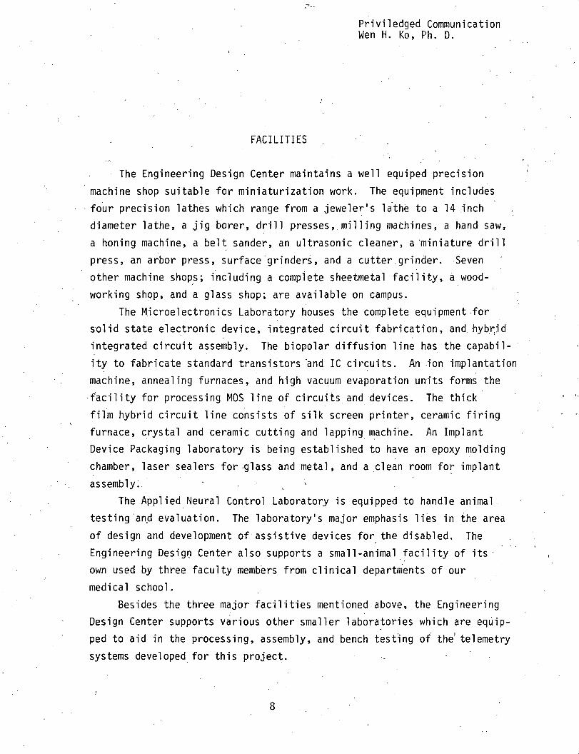
FACILITIES
The Engineering Design Center maintains a well equiped precision
machine shop suitable for miniaturization work. The equipment includes
four precision lathes which range from a jeweler's lathe to a 14 .inchdiameter lathe, a jig borer, drill presses, milling machines, a hand saw,
a honing machine, a belt sander, an ultrasonic cleaner, a miniature drill
press, an arbor press, surface grinders, and a cutter.grinder. Seven
other machine shops; including a complete sheetmetal facility, a wood-
working shop, and a glass shop; are available on campus.
The Microelectronics Laboratory houses the complete equipment forsolid state electronic device, integrated circuit fabrication, and hybrid
integrated circuit assembly. The biopolar diffusion line has the capabil-
ity to fabricate standard transistors 'and 1C circuits. An .ion implantation
machine, annealing furnaces, and high vacuum evaporation units forms the
facility for processing MOS line of circuits and devices. The thick
film hybrid circuit line consists of silk screen printer, ceramic firing
furnace, crystal and ceramic cutting and lapping machine. An ImplantDevice Packaging laboratory is being established to have an epoxy molding
chamber, laser sealers for-glass and metal, and a clean room for implant
assembly:. :-
The Applied Neural Control Laboratory is equipped to handle animal
testing and evaluation. The laboratory's major emphasis lies in the area
of design and development of assistive devices for the disabled. The
Engineering Design Center also supports a small-animal facility of its
own used by three faculty members from clinical departments of our
medical school.
Besides the three major facilities mentioned above, the Engineering
Design Center supports various other smaller laboratories which are equip-
ped to aid in the processing, assembly, and bench testing of the' telemetry
systems developed for this project. -
Rriviledged CommunicationWen H. Ko, Ph. D.
REFERENCES
1. McKay, R.S. Biomedical Telemetry. C.A. Caceres, Ed., New York:Press, 1970. .
2. Ko, W.H. and Neuman, M. "Implant Biotelemetry and Microelectronics."Science, Vol. 156, No. 3773, April 21, 1976, pp. 351-360.
j 3. Fryer, T.B. and Sandier, H. "A Review of Implant Telemetry Systems."Biotelemetry, 1(6), pp. 351-374.
4. Ko, W.H., Ramseth, D., and Yon, E. "A Multiple Channel MonolithicIntegrated Circuit Biomedical Telemetry System." 23rd ACEMB,November, 1970. •
5. Hoffmann, A. and Ko, W..H. "Design and Fabrication of a PAM/FMMultiple Channel Telemetry System." Twenty-eighth AnnualConference on Engineering in Medicine and Biology, NewOrleans, Louisiana, September 20-24, 1975.
6. Ko, W.H. NASA Annual Reports for NASA Grant Number NGR-36-027-053,1974, 1975. ' !-
7. Poon, C.W. "An Ingestible Temperature Telemetry System." M.S.Thesis, June, 1975. '
8. Guvenc, M.G. and Ko, W.H. "A Micropower Modulator Chip for Tempera-ture and Biopotential Telemetry." Twenty-eighth Annual Con-ference on Engineering in Medicine and Biology, New Orleans,Louisiana, September 20-24, 1975. -
9

Privi1 edged CommunicationWen H. Ko, Ph. D.
PROGRESS REPORTS
NGR-36-027-053
October 1, 1976 to September 30, 1977
10
... J

Priviledged CommunicationWen H. Ko, Ph. D.
. SINGLE FREQUENCY RF.POWERED ECG TELEMETRY SYSTEM
Introduction
The need for small and long-term telemetry transmitters, which could
be used to transmit physiological information from small animals used in ,
various biomedical experiments, imposes difficult restrictions on-the
construction of such devices. If the use of the implanted volume of
present telemetry units is analyzed, it can be seen that the battery or
equivalent energy storage generally occupies 50% of the volume, the elec-
tronics 25%, and the remainder is usually taken by the radio frequency
(RF) tank circuit; antennas; connectors and similar accessories. It is
therefore apparent that miniaturization of the electronics itself will '..
not be the complete answer to .the problem. Investigation carried out in
the Microelectronics Laboratory at the Engineering Design Center, in the.
past few years, has proven the feasibility of using an RF field to power
the implanted transmitter externally; especially when short range tele-
metry is used for data transmission from animals strapped in chairs or
moving in cages. The telemetry system using the external source of energytransmitted into the implant has the additional advantage in not being
limited in operation by battery lifetime and can therefore operate for the
total life span of the implanted electronic devices.
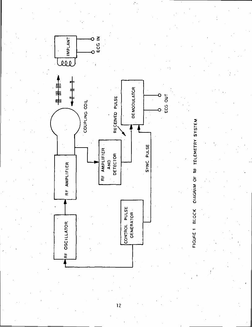
In order to reduce the volume of the implant unit and to simplifythe total equipment needed for such short range telemetry, an approach was
developed using a single RF frequency for energy transfer and signal
transmission. Only one tank circuit is used in the implant unit for both
functions; the RF energy absorption and data transmission. This is acomp-
lished by timesharing multiplexing as shown on the system block diagram
in Figure 1.
11
UJ
trUJ201_j-UJ
ULcc
uo_Jm
UJirOLi.
12
Priviledged CommunicationWen H. Ko, Ph. D.
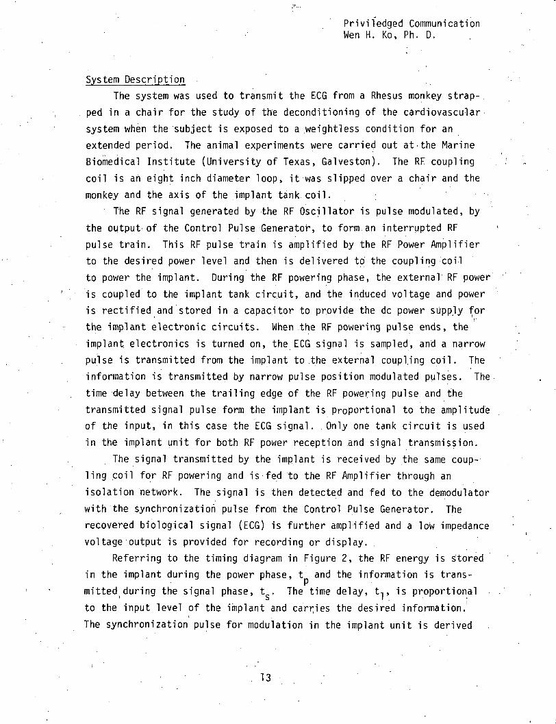
System Description
The system was used to transmit the ECG from a Rhesus monkey strap-,
ped in a chair for the study of the deconditioning of the cardiovascular
system when the subject is exposed to a .weightless condition for an
extended period. The animal experiments were carried out at•the Marine
Biomedical Institute (University of Texas, Galveston). The RF coupling
coil is an eight inch diameter loop, it was slipped over a chair and the
monkey and the axis of the implant tank coil. ;The RF signal generated by the RF Oscillator is pulse modulated, by
the output of the Control Pulse Generator, to form an interrupted RF
pulse train. This RF pulse train is amplified by the RF Power Amplifier
to the desired power level and then is delivered to the coupling coil
to power the implant. During the RF powering phase, the external RF power
is coupled to the implant tank circuit, and the induced voltage and poweris rectified and stored in a capacitor to provide the dc power supply for
the implant electronic circuits. When the RF powering pulse ends, the
implant electronics is turned on, the ECG signal is sampled, and a narrow
pulse is transmitted from the implant to the external coupling coil. The
information is transmitted by narrow pulse position modulated pulses. The
time delay between the trailing edge of the RF powering pulse and the
transmitted signal pulse form the implant is proportional to the amplitudeof the input, in this case the ECG signal. Only one tank circuit is used
in the implant unit for both RF power reception and signal transmission.
The signal transmitted by the implant is received by the same coup-
ling coil for RF powering and is fed to the RF Amplifier through an
isolation network. The signal is then detected and fed to the demodulator
with the synchronization pulse from the Control Pulse Generator. The
recovered biological signal (ECG) is further amplified and a low impedance
voltage output is provided for recording or display.Referring to the timing diagram in Figure 2, the RF energy is stored
in the implant during the power phase, t and the information is trans-
mittedi during the signal phase, t . The time delay, t-,, is proportional -
to the input level of the implant and carries the desired information.
The synchronization pulse for modulation in the implant unit is derived
13
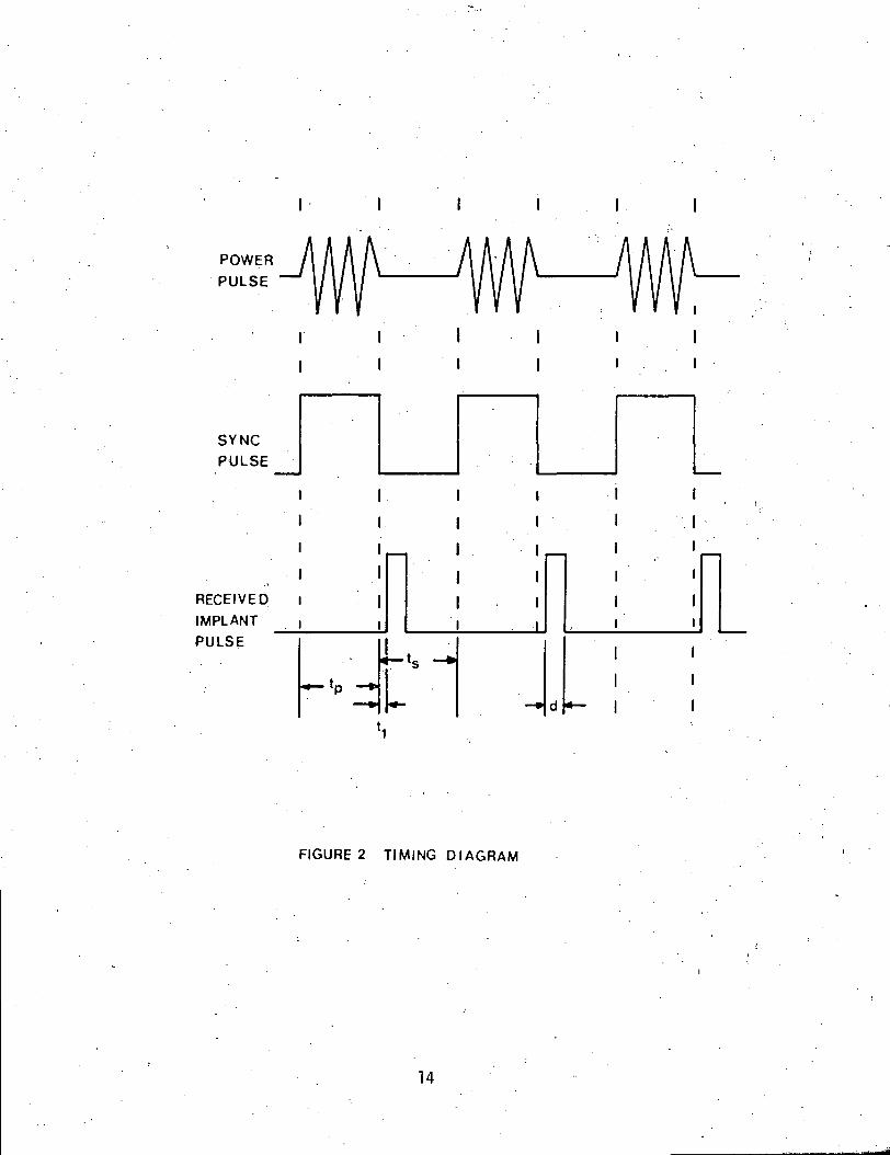
POWERPULSE
SYNCPULSE
1
.
RECEIVEDIMPLANTPULSE
1
*- p -*
1
1
1 1
«-ts -*
*- — »
-
d *-
1
1
1
1
FIGURE 2 TIMING DIAGRAM
14

Priviledged CommunicationWen H. Ko, Ph. D.
from the trailing edge of the power pulse; therefore, the system is in-
sensitive to small variations in the duration and period of the power
pulse. The value of the signal phase, t is selected with considerationof the maximum expected delay from the implant and power storage capa-
bility of the implant circuit. If "d" is the width of the transmitted
pulse from the implant and t, is the maximum expected delay, then the
condition for proper operation is t >t, +d. Furthermore, due to the
power supply regulation consideration it is desirable that energy con-
sumption during t be only a small fraction of the total stored energy
in the capacitor. Hence, t should not be much larger than t, +d. .
The time duration of the power phase, t , is not critical as long
as it is adequate to restore all the energy consumed during the signal
phase, t . Any variation of t will not introduce error into the trans-mitted signal. The value of "d" is determined by considering the power
consumption of the implant, range of transmission, and the signal band-.,
width of the RF amplifiers and the detectors of the external circuit.
Implant Unit . . '
The most important section of the implant transmitter is the oscil-lator. The same tank circuit has to be used for RF power detection and
also for oscillation and transmission of the signal. In addition, the
circuit has to generate a trigger pul'se coinciding with the trailing
edge of the RF power pulse which is needed for synchronization of the
modulator. .The complete circuit diagram for the oscillator is give in
Figure 3, the tank circuit is composed of L, C-, and C^-
The gate-drain junction of JFET Q-,, acts as a diode during power
phase t , when Q? is turned off. Q, serves as the RF power detector.
The rectified RF charge is stored in Cr and the voltage is stabilized by
the zener diode, D2- This stored power provides the power for the im-
plant circuit. A separate RF detector, D-, and C.,, is used to generatethe sync pulse for the modulator. When (L is turned on by the modulator,
during transmission period d, the RF signal is radiated or coupled to . '
the'external circuit through the tank circuit. Q-, operates as a'conven-tional Colpitts oscillator.
15

LUV)
CL
OOCo
oo o*-• 2
nu
cca
ucc
•oco'5
_J
u(/>o
UJQC
O
16
Priviledged CommunicationWen H. Ko, Ph. D.
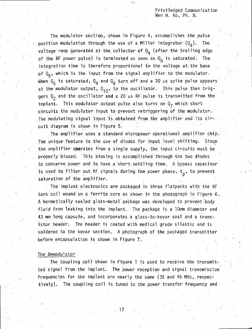
The modulator section, shown in Figure 4, accomplishes the pulse
position modulation through the use of a Miller integrator (Q4). The
voltage ramp generated at the collector of Q4 (after the trailing edge
of the RF power pulse) is terminated as soon as Q5 is saturated. The.
integration time is therefore proportional to the voltage at the base
of Qr, which is the input from the signal amplifier to the modulator.
When Q5 is saturated, Q^ and Qg turn off and a 20 ys spike pulse appears
at the modulator output, Q,Q, to the oscillator. Thi-s pulse then trig-
gers Qp and the oscillator and a 20 us RF pulse is transmitted from the
implant. This modulator output pulse also turns on Q, which, short
circuits the modulator input to prevent retriggering of the modulator.The modulating signal input is obtained from the amplifier and its cir-
cuit diagram is shown in Figure 5.
The amplifier uses a standard micropower operational amplifier chip.
The unique feature is the use of diodes for input level shifting. Since
the amplifier operates from a single supply, the input circuits must be
properly biased. This biasing is accomplished through the two diodes
to conserve power and to have a "short.settling time. A bypass capacitor
is used to filter out RF signals during the power phase, t , to preventsaturation of the amplifier.
The implant electronics are packaged in three flatpacks with the RF
tank coil wound on a ferrite core as shown in the photograph in Figure 6.A hermetically sealed glass-metal package was developed to prevent body
fluid from leaking into the implant. The package is a 10mm diameter and
43 mm long capsule, and incorporates a glass-to-kovar seal and a trans-
istor header. The header is coated with medical grade silastic and is
soldered to the kovar section. A photograph of the packaged transmitter
before encapsulation is shown in Figure 7.
The DemodulatorThe coupling coil shown in Figure 1 is used to receive the transmit-
ted signal from the implant. The power reception and signal transmission
frequencies for the implant are nearly the same (35 and 45 MHz, respec-tively). The coupling coil is tuned to the power transfer frequency and
. 17
CCo
CCO
uccocco
LUQCDO
u.
18

FIGURE 5 MODULATOR AMPLIFIERCIRCUIT DIAGRAM
19
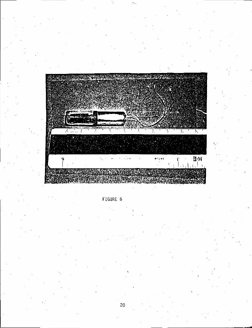
FIGURE 6
20

FIGURE 7 PACKAGED TRANSMITTER BEFORE ENCAPSULATION
21
Priviledged CommunicationWen H. Ko, Ph. D.
is not far from the data transmission frequency. The close proximity
between the coupling coil and the implant tank circuit (necessary for
good power transfer) provides a very strong received signal. The only
circuit necessary to detect the implant signal is a simple RF amplifier
tuned to the implant transmitter frequency and a diode detector (one
transistor). The RF amplifier and detector have a wide enough band-
width to eliminate the need for external tuning adjustments. The rest
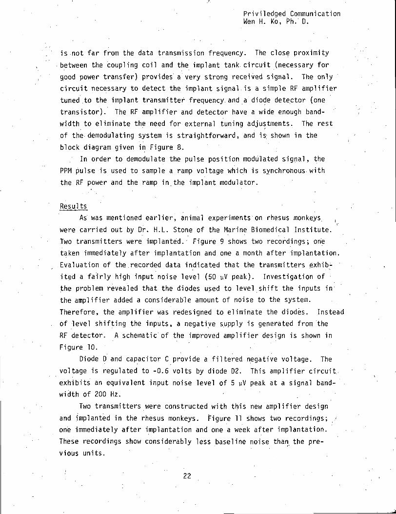
of the demodulating system is straightforward, and is; shown in the
block diagram given in Figure 8.
In order to demodulate the pulse position modulated signal, the
PPM pulse is used to sample a ramp voltage which is synchronous with
the RF power and the ramp in.the implant modulator.
ResultsAs was mentioned earlier, animal experiments on rhesus monkeys. ,
were carried out by Dr. H.L. Stone of the Marine Biomedical Institute.
Two transmitters were implanted. Figure 9 shows two recordings; onetaken immediately after implantation and one a month after implantation.
Evaluation of the.recorded data indicated that the transmitters exhib-
ited a fairly high input noise level (50 uV peak). Investigation of
the problem revealed that the diodes used to level shift the inputs in~the amplifier added a considerable amount of noise to the system.
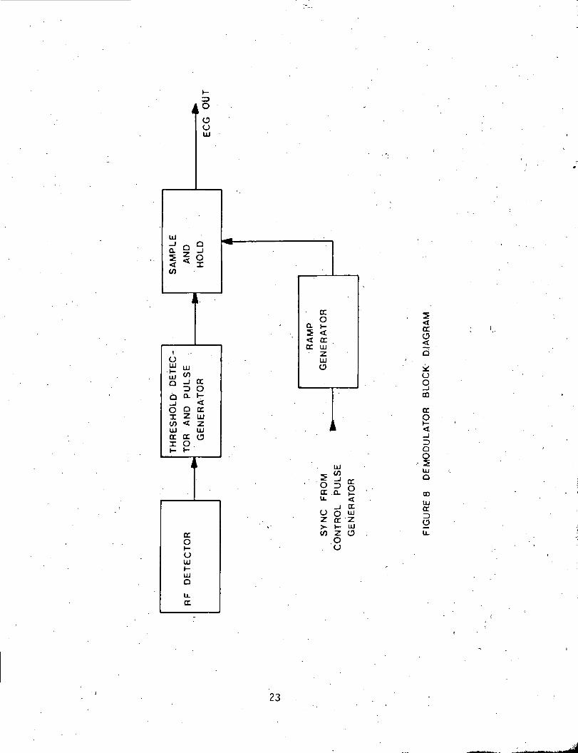
Therefore, the amplifier was redesigned to eliminate the diodes. Instead
of level shifting the inputs, a negative supply is generated from the
RF detector. A schematic of the improved amplifier design is shown in
Figure 10.
Diode D and capacitor C provide a filtered negative voltage. The
voltage is regulated to -0.6 volts by diode D2. This amplifier circuit
exhibits an equivalent input noise level of 5 yV peak at a signal band-width of 200 Hz. -
Two transmitters were constructed with this new amplifier design
and implanted in the rhesus monkeys. Figure 11 shows two recordings; <one immediately after implantation and one a week after implantation.
These recordings show considerably less baseline noise than the pre-
vious units.
22
1ooLULU
!<§CO
iO
Q cco
Q O. h-
0 O CCX Z LU10 < ZLU LUCC CC O1 O
CCO
a H2 << CCCC LU• z
LUO
cco
ogmcco
LU
E-°- g
ccOi-oLU(-LUoLL
CC
Z OC>- f-CO Zou
LUO
COLUCC
OLL
23

FIGURE 9.a EKG RECORDING -TAKEN IMMEDIATELY AFTER IMPLANTATION
FIGURE 9b EKG RECORDING TAKEN ONE MONTH AFTER IMPLANTATION
24
R1
>R2
R3
D)FROM >TANKCOIL
R7
R4
—•— KO -*-
I 5D2
R5
R6
FIGURE 10
25

FIGURE 11 a EKG RECORDING TAKEN IMMEDIATELY AFTER IMPLANTATION
—u-j—j—i
FIGURE lib EKG RECORDING TAKEN ONE WEEK AFTER IMPLANTATION
26

Priviledged CommunicationWen H. Ko, Ph. D.
Conclusion
The experiments carried out using the RF powered telemetry systemdemonstrate the feasibility of RF powered systems. After refinements
to the electronics, the system is providing good quality EKG record-
ings. The lifetime of the system is limited only by;the lifetime ofthe implanted electronics and package. The hermetic sealing of.the
package should provide good protection of the electronics and insure a
virtually indefinite lifetime. '
27
Priviledged Communication.Wen H. Ko, Ph. D.
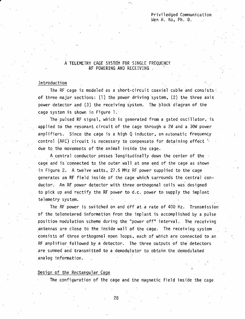
A TELEMETRY CAGE SYSTEM FOR SINGLE FREQUENCYRF POWERING AND RECEIVING . :
Introduction .
The RF cage is modeled as a short-circuit coaxial cable and consists '.
of three major sections: (1) the power driving system, (2) the three axis
power detector and (3) the receiving system. The block diagram of the
cage system is shown in Figure 1.'The pulsed RF signal, which is generated from a gated oscillator, is
applied to the resonant circuit of the cage through a 2W and a 30W power
amplifiers. Since the cage is a high Q inductor, an automatic frequency
control (AFC) circuit is necessary to compensate for detaining effect '<•
due to the movements of'the animal inside the cage.
A central conductor passes longitudinally down the center of the
cage and is 'connected to the outer wall at one end of the cage as shownin Figure 2. A twelve watts, 27.5 MHz RF power supplied to the cage
generates an RF field inside of the cage which surrounds the central con-
ductor. An RF power detector with three orthogonal coils was designed
to pick up and rectify the RF power to d.c. power to supply the implanttelemetry system. \
The RF power is switched on and off at.a rate of 400 Hz. Transmission
of the telemetered information from the implant is accomplished by a pulse
position modulation scheme during the "power off" interval. The receiving
antennas are close to the inside wall of the cage. The receiving system
consists of three orthogonal open loops, each of which are connected to an
RF amplifier followed by a detector. The three outputs of the detectors
are summed and transmitted to a demodulator to obtain the demodulated
analog information. . .
iDesign of the Rectangular Cage
The configuration of the cage and the magnetic field inside the cage
28

nor J-6j 'nii . i[nf!io3 bsubol i v'fi r!.(1 .in ,oM '.H nol-!
o
'.p
C.J-j -?.O IDU) O
M-01
Ul
O
Q
.0 <3 O
0~>"j
-U.'-ill
_j_]
0
ij!
r>V ;'! -•i Q ~2 ;! CD U> '
1 C_.t- — T •
1 t ' 10 }1 ' a> o f '
-•^ 1
i I "*! 1 ^ o! ' . 1 :V. ->"i . • . .').• "" — i
1 i •••' •! : "' u'
-'". •M -JJ» I'*? O ."" i
c;<••
\
Privi1 edged CommunicationWen H. Ko, Ph. D.
I
7.5 m
SIDE VIEW END VIEW
f\
j s } } j j j } j } j , s ) j j j } j v ; j s s s s j > s f jJ f/s I \ V, A
I I
Figure 2. THE CONFIGURATION OF THE CAGE
30
Priviledged CommunicationWen H. Ko, Ph. D.
are shown in Figure 2. The flowing path of the current I builds up amagnetic field B which is inversely proportional to the radial distance
from the central rod and is independent of the axial position. B is
given by:
B=-2-nr
where r is the radial distance from the central rod.If r is very small, B will be too high and so wi:ll DC pick-up voltage
(above five times the minimum value required). Then the regulator follow-
ing the detector will not be able to regulate the detected voltage within
the limited range. In addition, the resonant circuit of the cage would
be greatly detuned. Therefore, the central rod is surrounded by a plastic
tube so that the animal cannot reach this region.The rectangular cage with a size of 1m x .75m x .75m can be considered
as an end-shorted coaxial cable. As the length of the cage is much short-
er than the wavelength, the cage is a.high Q inductor. The equivalent
inductance is given by: .
L= b - .2TT (In a )
where 1 is the length of the cage (in meters)b is the equivalent, outer diameter of the cage
a.is the diameter of the central rod.
In this case, 1 = 1m; .b = 0.75m x —p— =^0.9 m
a = 1 inchhence, .1 = 0.79 yh. While the system is operating at 27.5 MHz the tuning
capacitance is 42 pf. The tuning circuit of the cage is shown below. The
Q of the resonant circuit is 90. . __- ,l
i . .
50ft
From power
11 pfj
T20 pf* I 10 pf
1
I 1
T r f\ _•£• I 1 1 i
0.79 yh'
amplifier 150 pf
Cage
31
Priviledged CommunicationWen H. Ko, Ph. D.
The mechanical construction of the cage is illustrated in Figure 3.
RF power is fed into the cage from one end of the cage. The receiver and
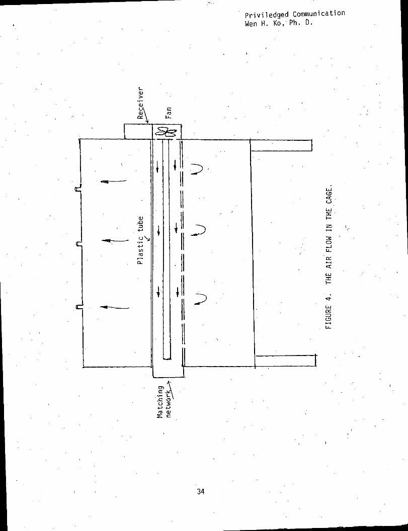
an electrical fan are mounted on the other end. The fan blows air into
the plastic tube through holes on the wall of the cage. Two rows of smallholes are drilled on the bottom of the plastic tube. Six pipes are on
the top of the cage. The air flow in the cage is shown in Figure 4.
The bottom of the cage is hinged at rear. It can be opened while clean-
ing. A row of rods are set three inches above the bottom for the conve-nience of cleaning.
Negative Feedback Loop For Automatic Frequency Control (AFC)
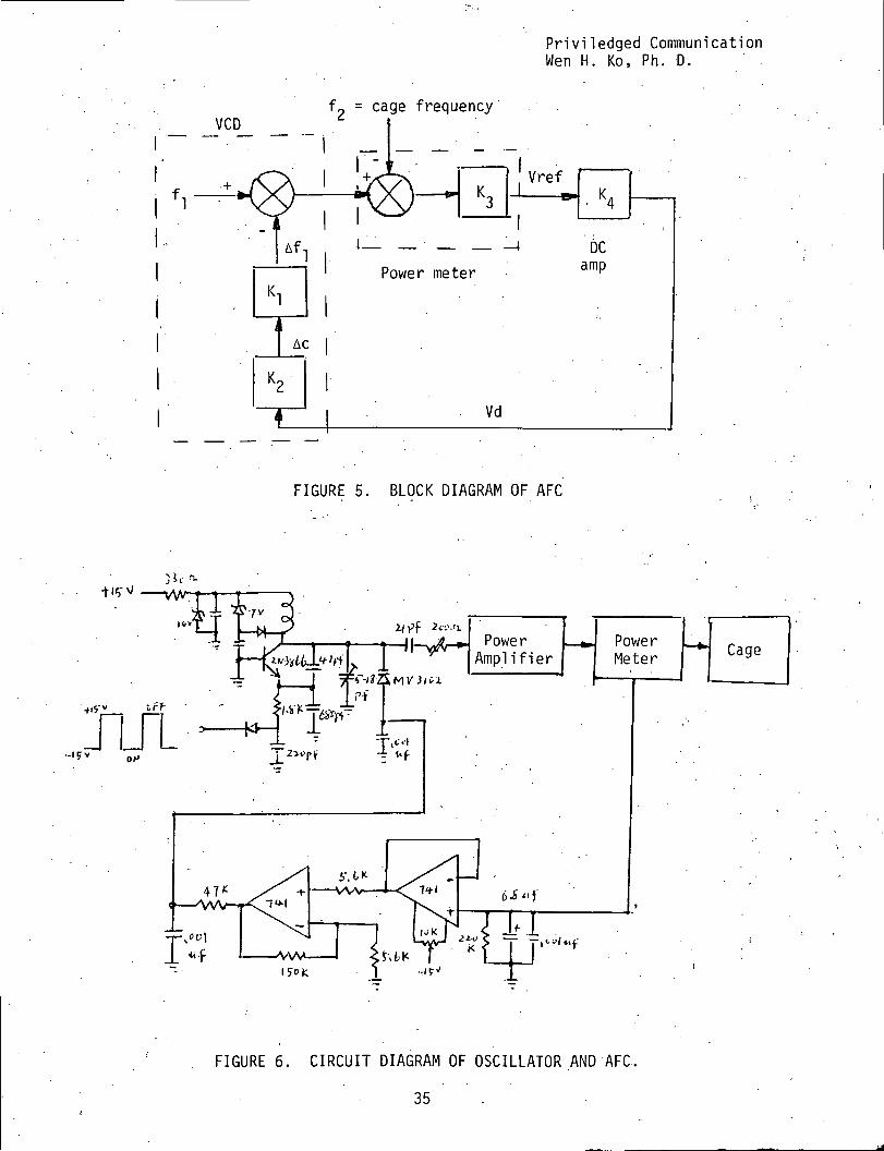
The AFC block diagram shown in Figure 5 would miminize the reflected
power by minimizing the frequency difference between the RF oscillator
and the cage resonant circuit. The d-.c. .-output voltage Vref of the powermeter WV-4, which is proportional to the square root of the reflected t
power, is used as the error signal of the negative feedback loop. Through
a low pass filter and a d.c. amplifier, Vref is amplified and the output
voltage V^ is applied to the voltage controlled RF oscillator. The cir-cuit diagram of the oscillator and AFC is shown in Figure 6.
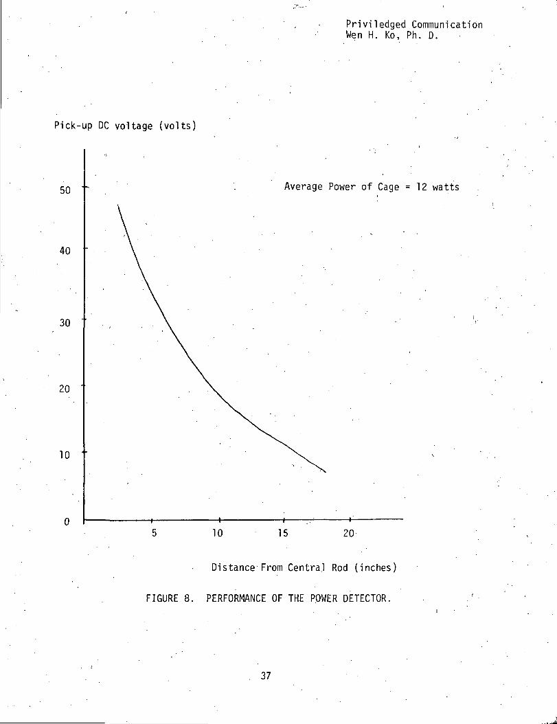
Three-axis Power Detector
The circuit and construction diagram of the three-axis power detector
are shown in Figure 7. Two perpendicular ferrite-core coils and an air-
core coil are utilized to pick up the pulsed RF power. The positions of
the three coils and the flat .pack of the transmitter are arranged to
minimize the mutual inductances and loading effects among them. In addi-
tion, a small air core coil, is required as the transmitting coil of the
implanted transmitter. The pick-up d.c. voltages of the three coils are
connected serially so that higher voltage can be obtained and the ripples
due to the variation of the direction of the power detector are reduced.
The two diodes for each coil make the circuit symmetrical. The three
tank circuits resonate at 27.5 MHz and have a loaded Q of 20. The per-
formance of the power detector is shown in Figure 8. For a single channel
EKG telemetry, a minimum voltage of 8 volts with a load current 100 yA isrequired.
- 32
Priviledged CommunicationWen H. Ko, Ph. D.
FIGURE 3. MECHANICAL DIAGRAM OF THE RF POWERED CAGE.
33
s_0)
QJ
03
o S4-> 4->rO (U5: c
Priviledged CommunicationWen H. Ko, Ph. D.
C_3
ce.roto
34
Privi1 edged CommunicationWen H. Ko, Ph. D.
VCD= cage frequency
I
Power meterDC
amp
Vd
FIGURE 5. BLOCK DIAGRAM OF AFC
t'T* —vW
FIGURE 6. CIRCUIT DIAGRAM OF OSCILLATOR AND AFC.
35

Priviledged CommunicationWen H. Ko, Ph. D.
TransmittingCore
\ Coil 1 Ferrite Coresif
\
Flatpack
Aircore
Coil 3
1.4"
1.3"
Single Channel Telemetry
Coil 1
Coil 2
Coil 3
EKG Signal
FIGURE 7. CIRCUIT AND CONSTRUCTION DIAGRAM OF THE POWER DETECTOR.
36
Pick-up DC voltage (volts)
Privi1 edged CommunicationWen H. Ko, Ph. D.
50
40
30
20
10
10
Average Power of Cage = 12 watts
15 20
Distance From Central Rod (inches)
FIGURE 8. PERFORMANCE OF THE POWER DETECTOR.
37

Priviledged CommunicationWen H. Ko, Ph. D.
To obtain the effective permeability as high as possible, the length
of the ferrite cores must be at least three times its diameter. In this.case, the diameter of the core is 1/4", the length is 3/4", and the
permeability of the material is about 30. Hence, the effective perme-
ability, ye, is determined by:
y_ •e
y0 1 + 0.1(y/yQ - 1)
Therefore, the area of the air-core is designed to be about eight timesthe cut area of the ferri.te-core. Then the three coils will, pick-up equalDC voltage. . . . ,
The three coils are specified as below:
Coil 1 and 2: Core: Size 3/4" x 1/4" x 3/16"
Permeability = 30 at 30 MHz
Wire: #28 . ,
No. of turn: 8 - 1/4
Coil 3: Core: Size 3/8" x 3/4" x 1/8"
Wire: #24
No. of turn: 10
Receiver •To receive strong enough signal independent of the position and
orientation of the transmitting coil, three orthogonal antennas of thereceiver are constructed as shown in Figure 9. They are made of copper
strips with width 1/4" and are built 1/2" apart from the grounded walls
of the cage to get high capacitive coupling with the transmitting coil.Through three 'coaxial cables, the three antennas are connected to the
inputs of three RF amplifiers respectively. •
A 3N128 and a MCI350 constitute the two stages RF amplifier which
has a gain 50 db. The low level detector, MC1330, is a doubly balanced,
synchronous detector featuring very linear detection. Its conversion
gain is 30 db. The tuning circuits in the receiver are all tuned at the
transmitting frequency, 48 MHz, and have a Q of ten. <
The three pulse outputs from the three detector are sent to a sum-
38

Privi1 edged CommunicationWen H. Ko, Ph. D..
*- To' receiver
FIGURE 9.' ANTENNAS OF. THE RECEIVER.
Antenna
AntennaRF Amp
Antenna
RF Amp. DetectorOIN 1 f.0
RF Amn
3N128
ni, i oou
RF Amn
MCI 350.
riU 1 J JU
Uc LcL UUr.
MCI 330
SummingAmp. To demodulator
FIGURE 10. BLOCK DIAGRAM OF THE RECEIVER.
39

Priviledged CommunicationWen H. Ko, Ph. D.
ming amplifier. The summed voltage is connected to a pulse position
demodulator, and is converted to the analog EKG signals. The block dia-
gram of the receiver is shown in Figure 10.
40 ,

Priviledged CommunicationWen H. Ko, Ph. D..
. A SINGLE FREQUENCY RF POWERED THREE CHANNEL TELEMETRY.SYSTEM
Introduction .
- Because of the relative large size and limited lifetime of conventional.battery
power, RF has become a very promising means of powering implant units and hence has
been extensively studied during the past years. This telemetry system stemmed from
the single channel RF powered telemetry,system developed use in MEL. In this part-
icular application, a single coil in the implant unit was used for both RF energy
absorption and signal transmission and therefore reduces the space needed for the
two-coil system - one for RF powering and another for signal transmitting at differ-
ent frequencies. A time sharing multiplexing technique was used.
The physiological events intended to be monitored includes aortic blood pressure,
body temperature and electrocardiograms. Aortic pressure normally requires'a '••
frequency range of about 40 Hz for meaningful recording, EKG needs about 80 Hz;
while body temperature is understood to be a very slow varying parameter. Work up
to now has included the system circuit design and system performance to bench"
stimulation. The remaining problem lies in the packaging area and further investi-
gation is being carried out.
System description •
A system block diagram is shown in Fig. 1. Pulse position modulation is used
for coding the information. Since the same frequency is used for RF powering and
signal transmitting, signal received by the demodulation unit will also consist of
these two components. The signal format is shown in Fig. 2.
Fig. 2
41

Privi1 edged CommunicationWen H. Ko, Ph. D.
Ill
(0
s- -oO) O> E
•r- QJOJ "Oo
5-O)X0)
Q.
S-O
co
n3N
•r—c:OS-.c:u
ento
oo
a>
oo
s_O)
oa.
Q.
Olo
c(O
42
Priviledged CommunicationWen H. Ko, Ph. D.
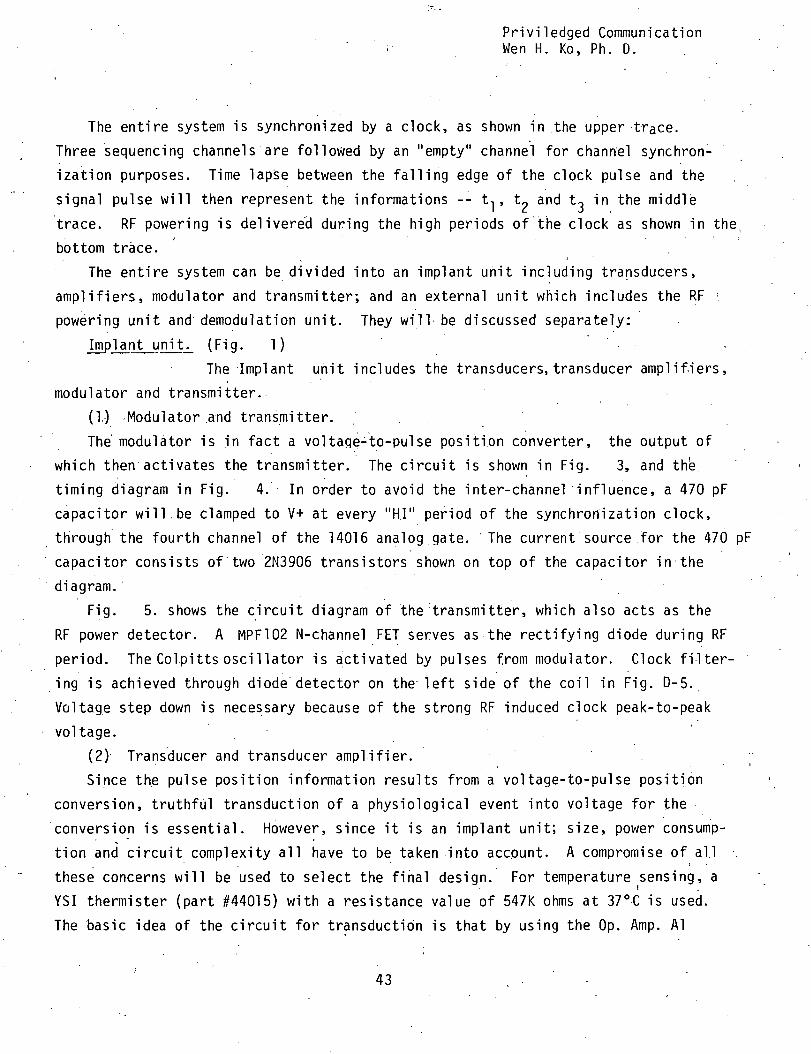
The entire system is synchronized by a clock, as shown in the upper trace.
Three sequencing channels are followed by an "empty" channel for channel synchron-
ization purposes. Time lapse between the falling edge of the clock pulse and the
signal pulse will then represent the informations -- t-,, t? and t-, in the middle
trace. RF powering is delivered during the high periods of the clock as shown in the.
bottom trace.The entire system can be divided into an implant unit including transducers,
amplifiers, modulator and transmitter; and an external unit which includes the RF •
powering unit and demodulation unit. They will be discussed separately:
Implant unit. (Fig. 1)
The Implant unit includes the transducers, transducer amplifiers,
modulator.and transmitter.
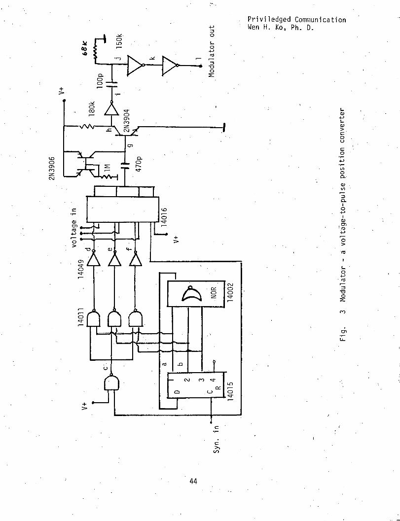
(1.) Modulator .and transmitter. .
The modulator is in fact a voltage-to-pulse position converter, the output of
which then activates the transmitter. The circuit is shown in Fig. 3, and the
timing diagram in Fig. 4. In order to avoid the inter-channel influence, a 470 pF
capacitor will be clamped to V+ at every "HI" period of the synchronization clock,
through the fourth channel of the 14016 analog gate. 'The current source .for the 470 pF
capacitor consists of two 2N3906 transistors shown on top of the capacitor in the
diagram.
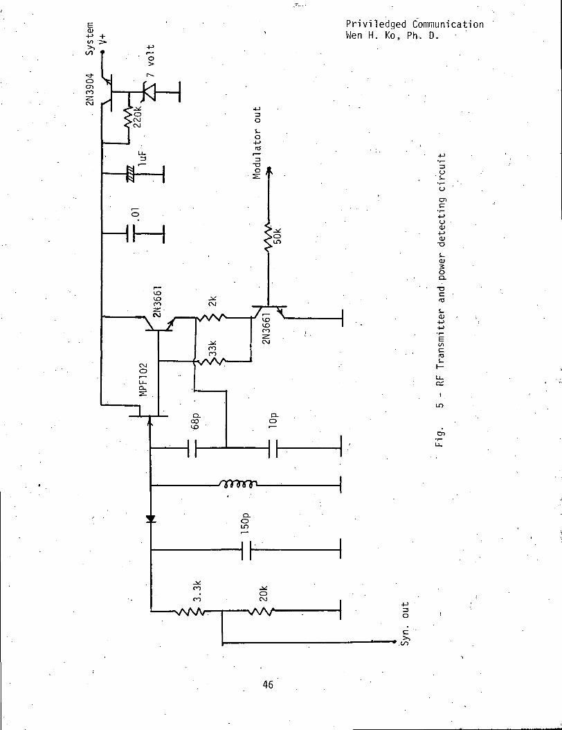
Fig. 5. shows the circuit diagram of the transmitter, which also acts as the
RF power detector. A MPF102 N-channel FET serves as the rectifying diode during RF
period. The Colpitts oscillator is activated by pulses from modulator. Clock filter-
ing is achieved through diode detector on the left side of the coil in Fig. D-5.
Voltage step down is necessary because of the strong RF induced clock peak-to-peak
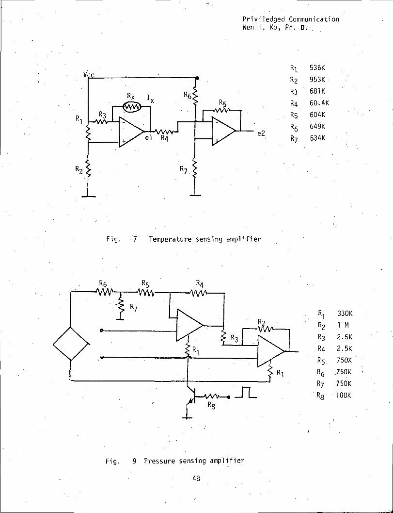
voltage.(2) Transducer and transducer amplifier.
Since the pulse position information results from a voltage-to-pulse position
conversion, truthful transduction of a physiological event into voltage for the
conversion is essential. However, since it is an implant unit; size, power consump-
tion and circuit complexity all have to be taken into account. A compromise of all -:these concerns will be used to select the final design. For temperature sensing, a
YSI thermister (part #44015) with a resistance value of 547K ohms at 37°C is used.
The basic idea of the circuit for transduction is that by using the Op. Amp. Al
43
Priviledged CommunicationWen H. Ko, Ph. D.
ocr>CO•z.CM
QJ+Ji-a>>coo
10OQ.
O)t/)
CLIO•MI
a>
o>
S-ofO
-oo
oo
44
Priviledged CommunicationWen H. Ko, Ph. D.
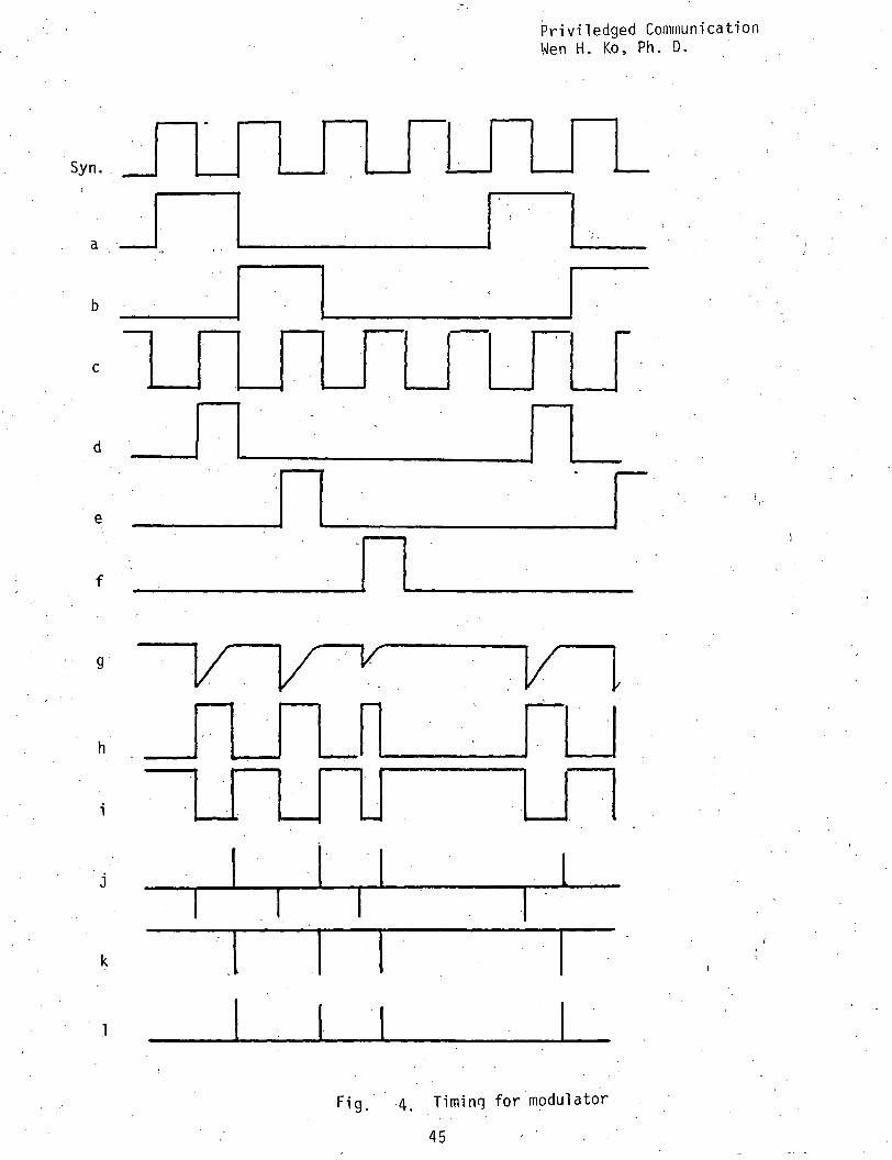
Syn.
rimV \
Fig. 4. Timinq for modulator
45
Privi1 edged CommunicationWen H. Ko, Ph. D.
o• s-O
Olc
o
OJ-as-01
oa.
s_O)
ECOC
a;iLO
en
Q.OID
CO -*£0
ro CM
0
c
46
Priviledged CommunciationWen H. Ko, Ph. D.
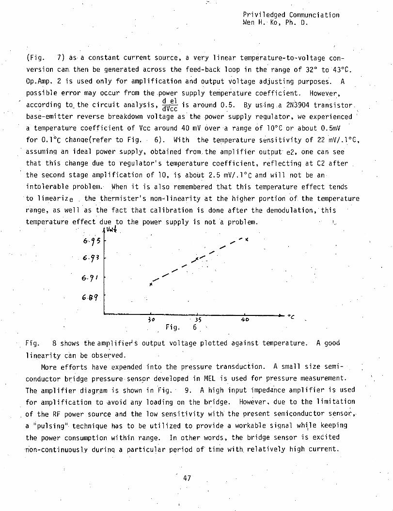
(Fig. 7) as a constant current source, a very linear temperature-to-voltage con-
version can then be generated across the feed-back loop in the range of 32° to 43°G.
Op.Amp. 2 is used only for amplification and output voltage adjusting purposes. A
possible error may occur from the .power supply temperature coefficient. However,d pi "according to, the circuit analysis, - is around 0.5. By using a 2N3904 transistor,
base-emitter reverse breakdown voltage as the power supply regulator, we experienced
a temperature coefficient of Vcc around 40 mV over a range of 10°G or about 0.5mV
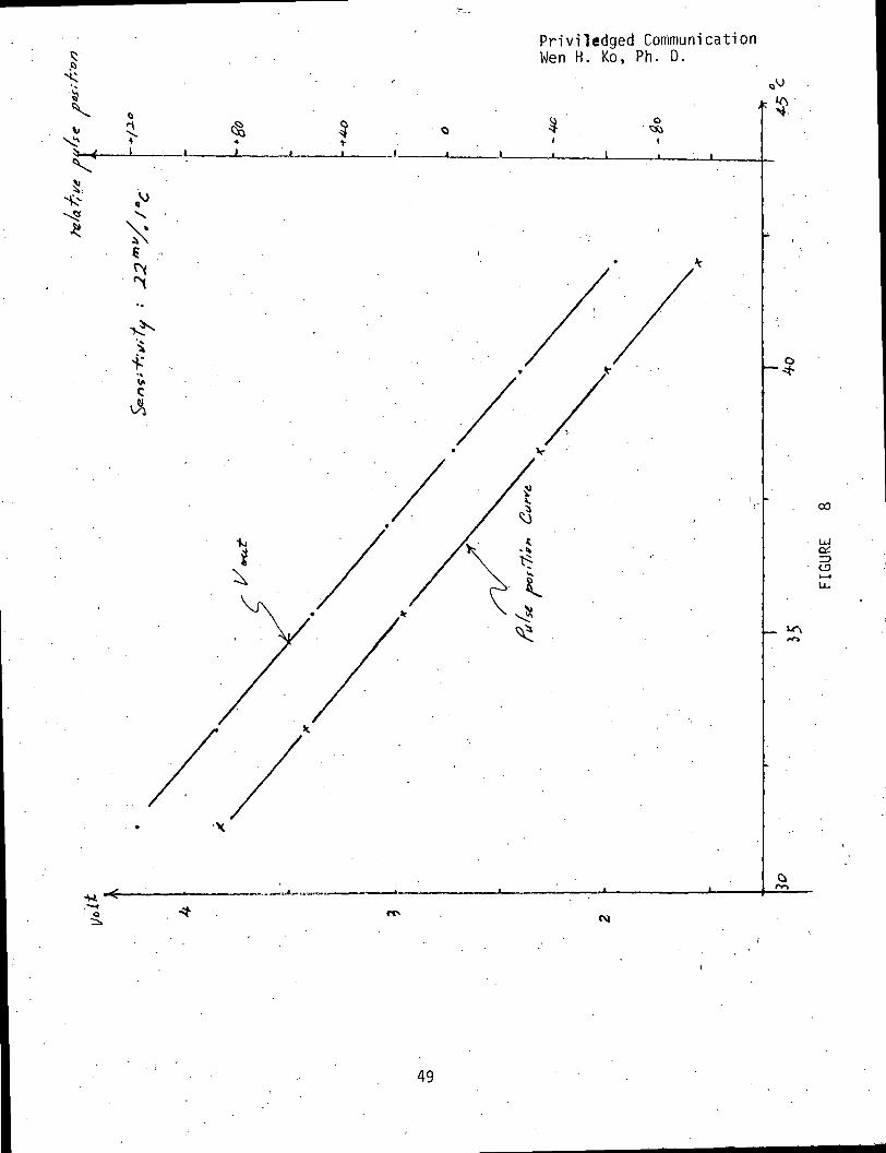
for 0.1°C change(refer to Fig. 6). With the temperature sensitivity of 22 mV/.l°G,
assuming an ideal power supply, obtained from, the amplifier output e2, one can seethat this change due to regulator's temperature coefficient, reflecting at C2 after .
the second stage amplification of 10, is about 2.5 mV/.l°C and will not be an
intolerable problem. When it is also remembered that this temperature effect tends
to linearize . the thermister's non-linearity at the higher portion of the temperature
range, as well as the fact that calibration is done after the demodulation, this
temperature effect due to the power supply is not a problem.
6 ?5
6-Jl
}0 35 40 c -Fig. 6
Fig. 8 shows the amplifier1 s output voltage plotted against temperature. A good
linearity can be observed.More efforts have expended into the pressure transduction. A small size semi-
conductor bridge pressure sensor developed in MEL is used for pressure measurement.
The amplifier diagram is shown in Fig. 9. A high input impedance amplifier is used
for amplification to avoid any loading on the bridge. However, due to the limitation
of the RF power source and the low sensitivity with the present semiconductor sensor,
a "pulsing" technique has to be utilized to provide a workable signal while keeping
the power consumption within range. In other words, the bridge sensor is excited
non-continuously during a particular period of time with relatively high current.
47
Priviledged CommunicationWen H. Ko, Ph. D. .
e2
R2R3R4
R5
536K
953K
681 K
60.4K
604K
649K
634K
Fig. 7 Temperature sensing amplifier
Revvv~-j 'ww
:-l R7
X «>X
/
•
•'Vvv^
r^LRi
i \AAA-v v v
' R3 h\Vw
1,J— VW— • J L
. R1 330K
" R2 1 M
R^ 2.5K
R4 2.5K
R5 750K
R6 .750K
R7 750K
R8 100K
Fig. 9 Pressure sensing amplifier
48
Priviledged CommunicationWen H. Ko, Ph. D.
>*
CO
en
49

Priviledged CommunicationWen H. Ko, Ph. D.
Sampling and holding is also achieved during this period. Timing for the bridge
pulsing is shown below in Fig. 10. '
IFig. 10
The pulsing achieved at the synchronous pulse stemmed from the rising edge of
this pulse. ,The bridge's power pulse length is about 100 AIsec and the excitation
current through the-bridge is about 3 riiA. A sampling window is opened at the end
of this pulse and is about 15 .usec. Pulsing again is applied to the I-set terminal
of the amplifier to obtain a fast settling time of the amplifier. Although with this
I-set value, the Op. Amp. has a,small signal gain band-width product of about 100 KHz,
the measured large signal gain bandwidth product is'only around 6 to 8 KHz. In view
of any sudden disturbance that might occur in the pressure, which may represent a
large signal rather than a small one, the amplification of the amplifier is restricted
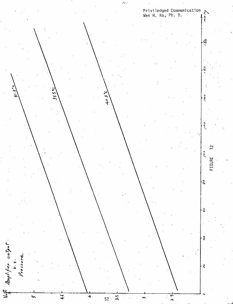
to about 400. The output swing voltage for 200 mmHg ranges about 2 volts . Fig- 11
shows the switching for bridge pulsing and Fig. 12 gives the amplifier's output
plotted against 200 mmHg pressure range. The significance of the temperature influence
on the transducer can also be seen from this. data. The compensation of the tempera-
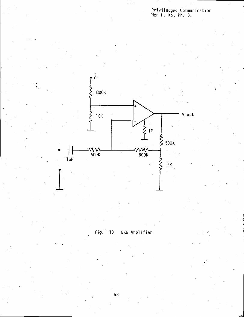
ture effect will be discussed later.The EKG amplifier is shown in Fig. 13. and is a conventional design.
External Unit
Demodulation and RF powering.
(1) Demodulation.The signal received bv the receiver, as mentioned, consists of the information
.signal .and RF signal. The format is shown below:
50

Priviledged CommunicationWen H. Ko, Ph. D.
k.
o•=3-
r L
AAA
Priviledged Communication ^Wen H. Ko, Ph. D. *
o;ZDCD
Priviledged CommunicationWen H. Ko, Ph. D.
V out
2K
Fig. 13 EKG Amplifier
53

Priviledged CommunicationWen H.' Kb, Ph. D.
Multiplexing of the channel is sequential and the period marked "p" .is the RF signal.
The block diagram for demodulation is shown in Fig. 14. The function of the
individual blocks are described as follows:
Antenna switch. As transmitting and powering are at the same frequency, a great
amplitude difference between these two signal sources exists.and protection of the AMreceiver is necessary. This is achieved by attenuating the RF powering signal received
by the antenna with a switching circuit (the circuit is shown in Fig.. 15). The control
for,switching is shown in pig. 16. Control pulses are generated from the clock.The format is as follows:
/ vThe n-channel MPF102 FET has a typical "ON" resistance at zero gate voltage, of .about
700 ohms channel resistance, and the typical "OFF" resistance at -7 volts is over
5 Mohms. When the control pulses go to low(-7 volts) level, n-channel FET MPF 102
is turned OFF',while p-channel enhancement mode MOSFET is ON. Conversely, at zero,
gate voltage the' P channel enhancement mode MOSFET has a typical "OFF" channel
resistance of greater than 100 Mohms and an "ON" resistance at -7 volts of less
than 0.5 Kohms. Consequently, the signal received by the antenna will be attenuated
when delivered to the receiver through this circuit if the applied gate voltage to
the two FETs is at zero volts, which in this case occurs during the RF powering period.
The attenuation was previously measured at about -90dB.
Threshold detector.- Fig. 17. This circuit serves both as. a threshold detector
and pulse level shifter - .due to the fact that the synchronous clock and receiving
signal pulses are 0 to Vcc peak-to-peak while the signal processing units operated
at IVcc. The purpose of this detector is to minimize .the noise resulting from .
transmitting and receiving process. A one shot is followed to adjust the pulse width
according to the sampling requirement. The present pulse width is set at 12 ysec.
Signal before
Threshold detector
Signal after
Threshold detector
' L HAUtAjuJ 1*—^ -4 ni ft f*- •- ' UsxvvWbw '
n54
Fig. 18

Priviledged CommunicationWen H. Ko, Ph. D. .
s_o4Joa>
l/lO)S-
OJUQJ
O+->
ro -r-C 2C 01CU
OJ
oS ininca
i. CL01
«*- 24- O3 _l
CQ
oin
OS
a.E
o
O.
ra1/5
C 1
s-o
4->fO
O)Ccu
Q.E
"3
Ere
CD
UO
co
XJo
toO)UO
C7)
I/)
55

Privi1 edged CommunicationWen H. Ko,..Ph. D.
Antennain
Controlin
2N4352 MPF 102
15 uH
100
AW—4
=f= c.OOli A 7V.
To receiver
regulator
. 15 uH
Fig 15 Antenna switch
20 k-
controlout
Fig. 16 Antenna switch control
56
O)t/1
Priviledged CommunicationWen H. Ko, Ph. D. .
S-o+JocuOJT3
-o'o_CI/)
S-
en
57

Priviledged CommunicationWen H. Ko, Ph. D.
Ramp generator. Information will be recovered from pulse position coding by
sampling the voltage along a ramp.
Fig. 19The ramp generator circuit is shown in Fig. 20. and it uses the stable zener diode
functioning voltage as a reference for the constant current supply source to charge the
capacitor over the feedback loop. From the circuit analysis, the ratio between the
zener's dynamic resistance (R,ivn ) and R^ (refer to Fig. 20), Ri/R(jyn> shouldideally be as large as possible. This means that for each practical zener, only one
optimum operating point is available. The zener presently used is a LM 103 2.4 volt
regulator which has a very low R • : in the range 10 ya to 10 ma.
Signal Processing. This part converts the sequencing pulse signal into three
independent channel pulses. A CMOS logic device is also used here.' The circuit
is shown in Fig. 21 and the timing diagram in Fig. 22. Since any signal in the
RF period represents errors, that period is blocked totally.
Sampling, hold-ing and buffer stage. - .Fig. 23. An analog gate is used for
.sampling; activated by the sampling pulse resulting from the signal processing block.
The CMOS 14016 analog, gate has an "ON" resistance of about 400Q and very high "OFF"
resistance. The input - output delay time is in the nanosec range.. The.holding
capacitor is 4700 pF, which during sampling gives an RC constant of about 2 psec.
The sampling time, as previously mentioned, is 12ysec. For the buffering stage,1 o
a 2H0042 FET Op. Amp is chosen because of its 10' .ft input resistance and very low
input bias current. A low pass filter with a high-cutoff at 120 Hz is followed to the,
buffer stage.Clock. The clock is generated by a 555 timer, shown in Fig. 24. The present
clock rate is set at 800 Hz, which gives a 200/sec sampling rate for each channel.
(2) RF Powering • • • ;
The power for the implant unit is supplied by RF -induction from a primary coil,
which is the external unit, into the secondary coil, which .is also the implant unit's
58

'Privi1 edged CommunicationWen H. Ko, Ph. D.
oD-
i.o
0)C.
fOon
oCM
59

Priviledged CommunicationWen H. Ko, Ph. D.
a
e
1
c
LL
f
M
Z/"
r
Ji
s
.,
(J )
u
Q
C >
•
)
A
^.J/
LT>
O<J-
a:
•»-l
vX'N
1
/
1
5
tr^xFl_/
\ 171
"XJ.- X
~~ ^\ r
A
Qi A. A•— 00
co
~\r~\ -WAA"! ~v
(/Icu
Q.
OJ
Q.E-(13
OO
.LLO
oc\jCO
CM00
-WWHooCO
TD C(L) •!-
-Ql
O)> -a)
0<
p—
>—CD
OS-
CTl-a-o
o;
.— Oo o^i- o
cu
(OCD
O) Q
c ca:
CU
CD
D;o
c3
CD
CUOoS-D.
CD
I/O
CXJ
60
Priviledged CommunicationWen H. Ko, Ph. D.
+7.5V
-7.5V
Fig. 22
ARamp
.+4V
,-4V
61
Priviledged CommunicationWen H. Ko, Ph. D.
t/lo;
I
•
OJ
cnenO(Octo
O)cr>
O)4-
"O
enc •
cr>c.
Q.Oo
COCM
o4->coo
«
c
Q. •
62

Priviledged CommunicationWen H. Ko, Ph. D.
-VCM
CM
"=fOO1CO
.CM
/VA—
UD0 «CDro
^ -^T CM
1 °J
1 .AA.
CDc
O)>OJ
LOCM
C7>
0)c
s_01cQJCD
OO
cr>
63
Priviledged CommunicationWen Hs Ko, Ph. D.
oo
Isio.
O
3O
O
cnc
OQ.
CO
cn
64

Priviledged CommunicationWen H. Ko,' Ph. D.
transmitting coil. Main consideration concentrates on the efficiency of the power
delivery, which depends on the Q values of the coils and the distance between the two
coils. The RF powering unit basically consists of an RF oscillator followed by a
power amplifier matched into the tuned primary tank. The circuit is. shown in Fig. 25.
System Performance
Power Supply (Vcc) Supply Current Clock rate
Implant ' •Unit 7 volt 250 yA " 800 Hz or 200/channel
ExternalUnit ±7.5 volt 45 mA 800 Hz
Two approaches were used to evaluate the system's performance. The.first was mainly
aimed at the electronic circuits. Instead of using the transduced voltage, signal from
the function generator is directly fed into the modulator input and monitors the system's
output with a sinusoidal wave. Frequency response is of main interest here. Fig- 26
shows the output recording of two arbitrary channels of the three available channels.
The performance of the system can be summarized as follows:
1. 60 cycle noise: ,
.This is mainly due to the power supply ripple of the demodulation circuit.
The decoupling circuit had been used for each circuit board. The 60 cycle noise seen
at the output is less than 5 mV.
2. Cross talk:With an input of a 5 volt peak-to-peak sinusoidal wave, the cross talk measured
is about -60dB, which is also the typical CMOS multiplexor value.
3. Line coupling noise:
The output of the scope appears as spikes, the amplitude is about 15 - 20 mV.
Since it is measured after the 120 Hz High-cutoff low pass RC filter, probe pick-up
is of high possibility.
65
Priviledged CommunicationWen H. Ko, Ph. D.
4. Sensitivity: -
Sensitivity is defined here as ~ ^ .- . It "is dependent on the degree of pulse-
position modulation and also the slope of the sampling ramp. With the present setting
the sensitivity is about 0.75.
5. Frequency response: • ''; ,
Different input frequencies were applied and the system output was recorded:,
(The sampling rate of the data was set at 300/sec when taking this data). Since the
information content is well within 100 Hz, any frequency higher than this was not',
tested. The attenuation of the higher frequency shown in Fig- 26, is mainly due to
the frequency response roll-down of the chart recorder.
6. Sampling, holding drift:
The holding capacitor is 4700 pF. The only discharging pathways are through the
buffer amplifier input and the analog gate. Both of these have a resistance value of
greater than 10^ ohms. RC constant in any event should be larger than 20 seconds.
The drift seen at the output is less than 4 mV. '.. '
7. The pulse position linearity is shown in Fig. -27. It shows that the con-
version factor is 16 mV for 1 psec pulse position change.
The second approach to test the system has the sense of completion since it
includes the transducer stage. The entire implant unit is placed.into the oven for
controlled temperature testing. The pressure transducer was kept in. a well-sealed
test tube with a variable pressure arrangement. The EKG channel is grounded. . The
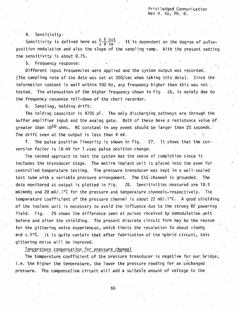
data monitored at output is plotted in Fig. 28. Sensitivities measured are 10.9
mV/mmHg and 20 mV/.l°C for the pressure.and temperature channels.respectively. The
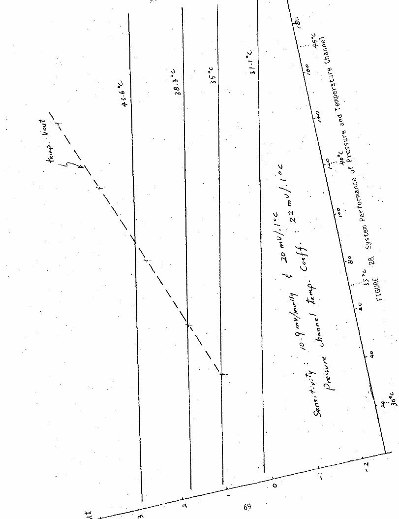
temperature coefficient of the pressure channel is about 22 mV/.l°C. A good shielding
of the implant unit is necessary to avoid the influence due to the strong RF powering
field. Fig. 29 shows the difference seen at pulses received by demodulation unit
before and after the shielding. The present discrete circuit form may be the reason
for the gittering noise experienced,, which limits the resolution to about ±lmmHg
and ±.1°C. It is quite certain that after fabrication of the hybrid circuit, this
gittering noise will be improved.
Je_m£e_rature_ compensation for pressure channel
The temperature coefficient of the pressure transducer is negative for our bridge,
i.e. the higher the temperature, the lower the pressure reading for an unchanged
pressure. The compensation circuit will add a suitable amount of voltage to the
66

~L h-- _"1" ' '^ I ~l i i i.M ! . . - - -W"
I :. . I . i .-. ! . I , i
Lj_!_:i_i_i.,q.2.«*, ., I., 2 Jz, :I
/ v I!
T
j—
!
1 ' . i
V u iy\ d ; i
\ f\ (\
1
V i v i !
fIV
i ' ! ' ;• i > : !
III!1IIKKIIIII
(1(1
y
( : ! ' " •
20 Hz I 40 Hz. I t : . . . . . .
i : i ' i :i
; J
! :
. ..... .... ......
1 •- i ,i l : :
• ; • - < : i : • • i • i :A A A A A A A
V . V
Fig. 26 Frequency test. Recording of arbitrarytwo channels.
67

I (>0
4.0
* p
/
Priviledged CommunicationWen H. Ko, Ph. D.
. 3
FIGURE 27
68
0ft
rf>
o \
\\
"f--
\\\
\\\
\
\
\
\
\
\
O
•
6Q),
a)
1v•O
(0
0)
rV
vfl,o CD» V
<D '
o
via •
0 .-o a)
ex-
\'(to CO
0P
cDV-*
u-
>> V
Priviledged CommunicationWen H. Ko, Ph. D.
After the shielding
Before the shieldingFig. -29 Shielding effect of the transducer amplifier
70
Priviledged CommunicationWen H. Ko, Ph. D.
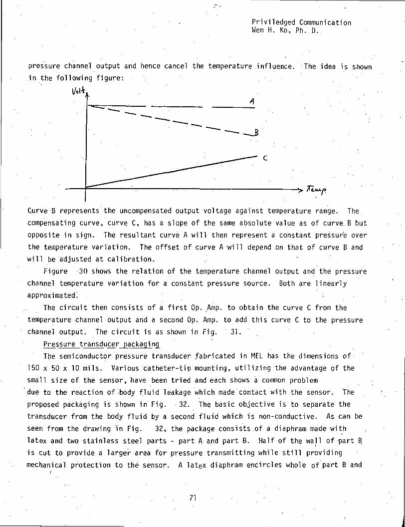
pressure channel output and hence cancel the temperature influence. The idea is shownin the following figure:
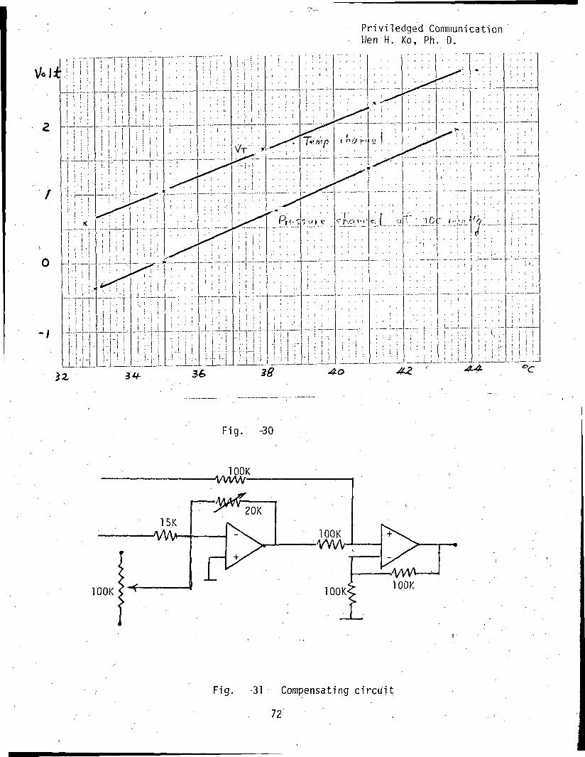
Curve B represents the uncompensated output voltage against temperature range. The
compensating curve, curve C, has a slope of the same absolute value as of curve, B but
opposite in sign. The resultant curve A will then represent a constant pressure over
the temperature variation. The offset of curve A will depend on that of curve B andwill be adjusted at calibration. '
Figure -30 shows the relation of the temperature channel output and the pressure
channel temperature variation for a constant pressure source. Both are linearly
approximated'. -
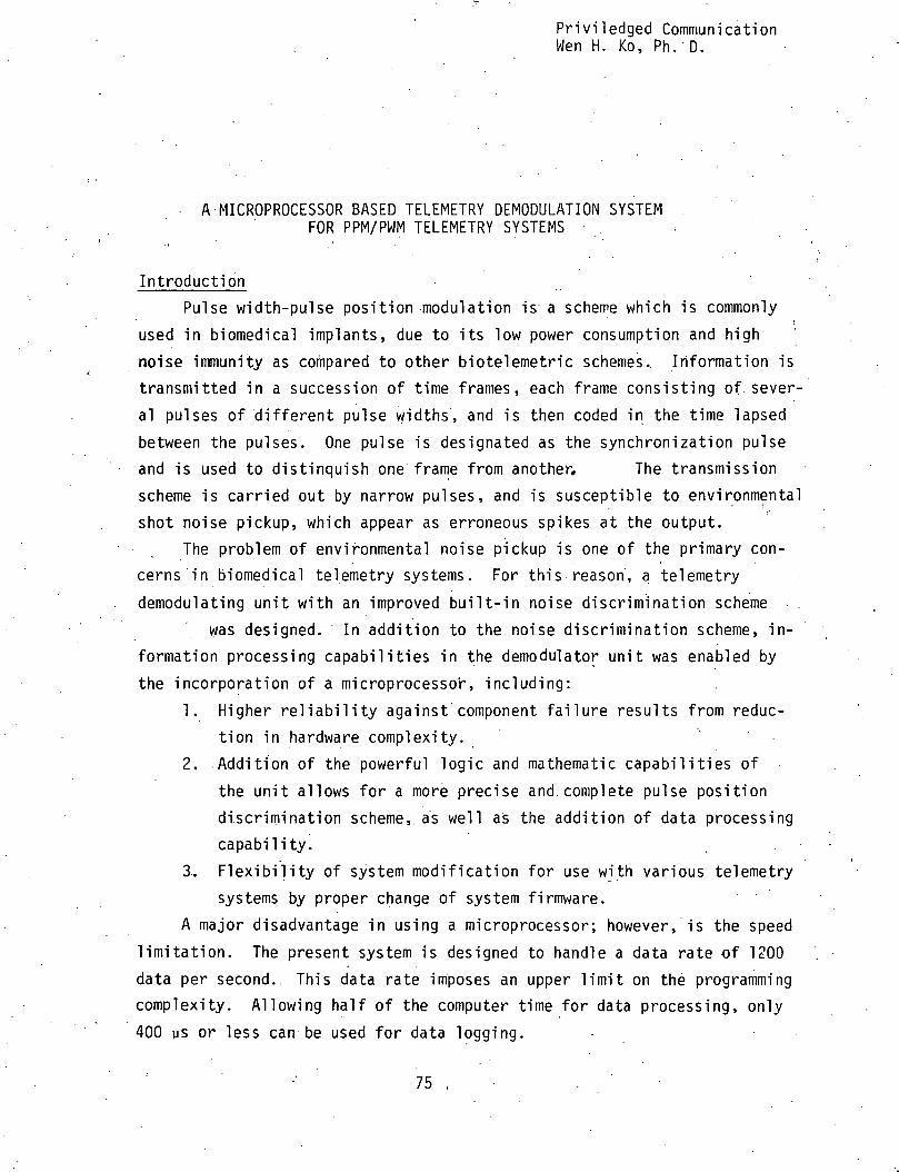
The circuit then consists of a first Op. ,Amp. to obtain the curve C from the
temperature channel output and a second Op. Amp. to add this curve C to the pressure
channel output. The circuit is as shown in Fig. 31.
Pressure transducer packaging
The semiconductor pressure transducer fabricated in MEL has the dimensions of
150 x 50 x 10 mils. Various "catheter-tip mounting, utilizing the advantage of the
small size of the sensor, have been tried and each shows a common problem
.due to the reaction of^body fluid leakage which made contact with the sensor. The
proposed packaging is shown in Fig. -32. The basic objective is to separate the
transducer from the body fluid by a second fluid which is non-conductive. As can be
seen from the drawing in Fig. 32, the package consists.of a diaphram made with
latex and two stainless steel parts - part A and part B. Half of the wall of part B
is cut to provide a larger area for pressure transmitting while still providing
mechanical protection to the sensor. A latex diaphram encircles whole of part B and
71
Priviledged CommunicationWerrH. Ko, Ph. D.
Fig. -30
15K-vi/v-
100K
vwwOK
20K
100K-vwv-1-
100K
Fig. -31 Compensating circuit
72

Priviledged CommunicationWen H. Ko, Ph. D.
Latex Diaphram
Finishing outlook
Part B.
Part A.. I
Fig. 32Pressure transducer
packaging assembly
transducer
73

Priviledged CommunicationWen H. KOi Ph. D.
is bonded to its base. Sensor leads run through the center hole of part A. The holeis then sealed with RTV. The sensor rests on top of part A with a distance.of about2 mm. Sensor leads also serve as the supporting structure. The inside space is filledwith silicon grease, which is the above mentioned "second fluid". The sealing processwill be done in the silicon grease in the vacuum to insure that no air bubbles will betrapped inside the package.
The entire unit at present has a diameter of 160 mils and. is 500 mils in length.'However, it is only the first unit under test and it is believed that further sizereduction can be obtained after successful development of the entire procedure.
74
Priviledged CommunicationWen H. Ko, Ph. D.
A MICROPROCESSOR BASED TELEMETRY DEMODULATION SYSTEMFOR PPM/PWM TELEMETRY SYSTEMS •
IntroductionPulse width-pulse position^modulation is a scheme which is commonly
used in biomedical implants, due to its low power consumption and high
noise immunity as compared to other biotelemetric schemes.. Information istransmitted in a succession of time frames, each frame consisting of sever-
al pulses of different pulse widths, and is then coded in the time lapsed
between the pulses. One pulse is designated as the synchronization pulseand is used to distinquish one frame from another. The transmission
scheme is carried out by narrow pulses, and is susceptible to environmental
shot noise pickup, which appear as erroneous spikes at the output.The problem of environmental noise pickup is one of the primary con-
cerns in biomedical telemetry systems. For this reason, a telemetry
demodulating unit with an improved built-in noise discrimination scheme
was designed. In addition to the noise discrimination scheme, in-
formation processing capabilities in the demodulator unit was enabled by
the incorporation of a microprocessor, including:
1. Higher reliability against component failure results from reduc-
tion in hardware complexity.
2. Addition of the powerful logic and mathematic capabilities of
the unit allows for a more precise and.complete pulse position
discrimination scheme,, as well as the addition of data processing
capability.
3. Flexibility of system modification for use with various telemetry
systems by proper change of system firmware.
A major disadvantage in using a microprocessor; however, is the speed
limitation. The present system is designed to handle a data rate of 1200
data per second. This data rate imposes an upper limit on the programmingcomplexity. Allowing half of the computer time for data processing, only
400 gs or less can be used for data logging.
75 , . " •

Priviledged CommunicationWen H. Ko, Ph. D.
The demodulator unit does not aim at one particular telemetry signal,
but aims at a class of signals which are coded in a pulse width-pulse
position modulated scheme. To provide such flexibility, three channels
of pulse width discriminators are supplied. To insure high reliability,
the system initiates a set of self-checking tests during the'••power upand reset stages. Software has been implemented in the system for a
three channel RF powering telemetry unit, which has been developed at
the Engineering .Design Center. The physiological parameters which aremonitored include: ECG, aortic blood pressure and body temperature.
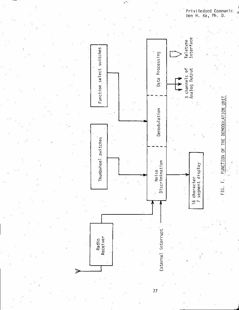
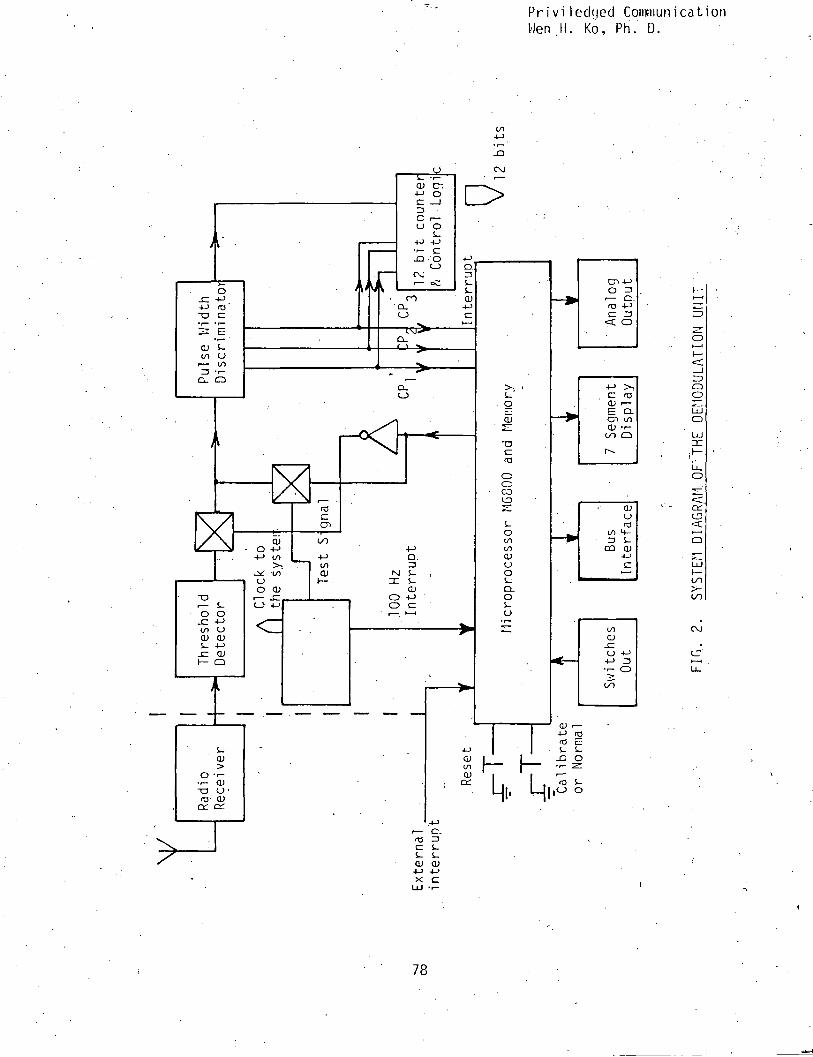
A functional block diagram and a system block diagram of the micro-
processor based demodulation system are given in Figures 1 and 2,
respectively. Basically, the system performs four distinct funtions:
(1) noise discrimination-distinquishes signal from noise, (2) signal
demodulation-converts the pulse position modulated signals into physical
parameters, e.g. temperature, (3) information processing-processes infor-
mation for display and recording, and (4) system self-checking. System
blocks include the noise discrimination scheme. System clock micro-
processor and associated memory, test signal unit, input switches, andsystem output.
SYSTEM HARDWARE
Noise Discrimination Scheme
The noise discrimination scheme consists of a threshold detector,
pulse width discriminator,'and pulse rate discriminator. The threshold
detector (Figure 3) is used to establish the proper amplitude of the
incoming signal. Signals from the radio receiver are buffered by an LM310
voltage follower, which in turn drives the base of an NPN switching tran-
sistor (2N3904). The transistor is turned on when the input signal is
greater than the sum of V and V, , where V is the voltage across C..
When the capacitor is charged to the peak signal value, the difference of
the input voltage and V, , the transistor is turned off. During the
transistor off time, the capacitor discharges with a time constant RtC,,
until the next input pulse. To isolate loading effects of the following
76
Priviledged CommunicHen H. Ko, Ph. D.
ooCU-Cu
4->
00
_,_,
OCD
OJ00
0
+->(J
13Li-
ni
onCU
O
5
'oJCD-.c
JDE
_c
t-O OJ•r- >-a ••-ro O)o; o
01a;
\
' CDC
•i —00
tuOS-o
ro4-)
Q:
— » -• ^ «•
co
^
, o
a
— — —
c •o
'1—+J
CD ro
.J2 .0 E
tlU00
'r—, Q
ai o• CL. ro
>•.**--t-5 i-QJ OJ
> i — -MCU C
14_ 4JO 3
C-OO -I-
5
E - =CU OcC CD
5 °.O ro
Cro <'
ro"
'o.r» ^
s- -ocu4-) 4-^ 'o c:ro CUi- Ero CD
• .C CUO oo
ti i i-o r^
+->o.
S-^_O)+Jc•r-
r^ ;
ro :
S- ICU
4_>
OO
o
o
77
Privi ledqecl CommunicationWen.H. Ko, Ph. D.
X/
—
Q_
I
\?/
^o.C
QJ
JC
1
o ••r—
roc£
\
>-
ro
k:
tor-LJ
^
/Vk
\
O
QJ4->QJ
i-QJ
QJ0'OJ3;
roc:C71
QJ CO• O 4->
4-> CO 4->>- ^~1 to
^ VI QJ
r—O QJ
C_3 4->
<~^>~_ - . . ~
_ . _
,J
/^vJ
t j
.X»V
^
^
/•-J
h.
(-C^—
—
Q.C_
D.
O-(
J
>).
^_QJ4->
CU
0
CN.
'
ro
>
^
^
>
4->Q.3S_
OJ
c— «
—
«s_QJ
cr.0i
oS-
o<_)
Ov_
)
C.
s_s_QJ
C
^JQ.^3
^~
C
^^
>_.
QJl/lO)
^>
>v '
O
^c:ro
C
COIO
U
v-iQJOO
Q.0i-u
'' "
"I1-LI
w
-
4-> nrO cS- S.
-O C•r~ *±
fO S,0 C
i — Cro 4->C 13
=C 0
C roOJ i—E Q,C7l l/lO) -r-
QJ
rO
• 3 S-D3 QJ
QJ-C(J 4J
•r- 0
l/l
3
2
3
Oo
LL_O
UJf-C/1
78

Privi1 edged CommimicoWen H. Ko, Ph. D.
OUJI—UJQ
QI
O
Co
EO O$-'•!- S-
4- TD O)
CD79

Priviledged CommunicationWen H. Ko, Ph. D.
stages from affecting.the decay time, V is buffered. The 741 operation-
al amplifier sums V and V. m which is defined to be the maximum ampli- .L- U"
tude. The threshold level is determined by taking approximately two-
thirds of the maximum amplitude with potentiometer P.,- A v.oltage
comparator (yA710) is used to compare incoming signals with the thres-
hold level. The threshold detector is limited in that the strength of-i
the incoming signals must be greater than the base-emitter voltage of the
NPN switching transistor. It is further limited in that slight, distortion
and delay of the pulse shape exists due to the finite switching speeds of
the transistors and operational amplifiers.
The pulse width discriminators (Figure 4) are used to setup pulse
width windows for the incoming signals. This serves the dual purpose of
distinquishing the occurrence of different pulses, as well as noise. Only
pulses within the pulse width windows are allowed to pass each monostables.The microprocessor is responsible for proper loading of the pulse; widths
(
into a set of D-latches to set the lower limits and tolerance of the
discriminator. There are three sets of pulse width discriminator in the
system. The first set differs from the other two in that its first mono-
stable has three cascading binary counters; while the others only have
two. This provision was made to allow for systems with a wide synchronous
pulse. The present system allows for synchronous pulse widths of 0-2048' ys;
with a maximum tolerance of 16 ys.
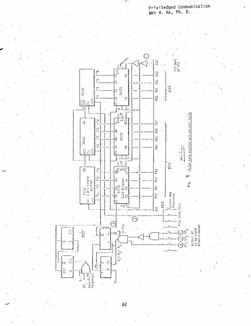
The pulse rate discriminator (Figure 5) is used to compare the pulse
rate of incoming signals with the pulse rate of past signals. The pulse
position counter is formed by three binary up counters. .An on-board dip
switch is provided for selection of the counter clock frequency. This
provision is made to allow for optimal choice of the clock frequency for
various telemetry systems.
System Clock and Microprocessor System
Accurate timing is necessary for counting the time lapsed between
pulses. A clocking system was designed based on a 4 MHz crystal and a-
MC4324 voltage control oscillator. The circuit diagram of the system
clock is given in Fig. 6* Output from the voltage control oscilla-
80

Privi1 edged CommunicationWen H. Ko, Ph. D.
81
Priviledged CommunicationWen H. Ko, Ph. D.
82

Priviledged CommunicationsHen H. Ko, Ph. D.
CM
03
UJ
^S
CM
OJ
JD03C
LiJ
O'
- »LO
'03 . oo
? r~i— L- -
"~ «a-
r-
<CJ !
t(
C.
'
QJT3 CM
OO 03 ~ .oo cjE: QJ s-O O QJ
CO r— C ir — 03 3t_JLO ZJ O•ci- Q <_)
CM C*1
QJ 'T3
O Ur: QJ i-C_3 Q QJ
CO r — Cr— 03 ZJ
QJ LO 3 O
_o03.
1 1 \ o
L_ f~^
LU.
n ' J*c C-
UJ
-— C'
S- <Cr— i«i O"LJ t_)
O
-M "O
O 5-<_> O
CM 03 i —n -t-> •<—^- i — Ut_J O 00
^ > °
D- C
J *+ — '
+JQJl/l
S
l 1
+->
00QJo:
CxJ
Xi<_)
-(->QJ
QJ
t
N C.
r^ ^ ?1 *> 0 C
O QJ
]l. C
0
LO
03
crQJ
1 ^1 ^
4->"O -v^
— Ik ^ Sr QJ C)
00
3 UJ••U_ 1 —
1 — 111
Q. (—
m 1 1C O
ON ' "~un z: -*-1 nCM n on <c
+-> CJDON <=rLT> z; QJ Q
4->
• N oo h-
H CO ZD
rr oCM
'' VO
'u.
IllII"
^- 1 __, Lj
~T~ n
LO
Hi-
83
Priv'iledged CommunicationWen H. Ko, Ph. D.
tor is fed into a 74161 decade counter, providing a 2 MHz, 1 MHz, and
500 KHz clock. The MHz output is fed into two 4518 dual CMOS counters,
providing a 100 Hz clock to interrupt the microprocessor and a test .
signal to the system [40 usec. at 1 KHz rate].The microprocessor unit (MPU) was designed with the capability of
programming development, field testing and easy system modification. The
system block diagram is given in Figure 7. The packaging of the unit is
modular, to allow for system expansion, as well as ease in troubleshooting.
The peripheral inputs and outputs are divided into two groups. The first
group consists of all of the thumbwheel and pushbutton switches which aretreated as memory addresses and hang directly on the address bus. The
second group of peripheral inputs and outputs require data handling and
handshaking and communicate with the microprocessor via two peripheral
interface adaptors. These inputs and outputs include the interrupt signals
from the pulse width discriminators, inputs from the counters, pulse• • idiscrimination setting and D/A converter outputs.
The MPU is controlled by a two phase, non-overlapping clock, which
is provided by a retriggerable monostable in an astable configuration.
Two potentiometers are used to adjust the pulse widths of $-, and ty?- The
minimum pulse widths for <f>, and 4>2 are 430 ns and 450 ns, respectively.
As the access time of the PROM 1702 exceeds 1000 ns, $„ is lengthened to
1000 ns to insure proper data reading. A power up resset circuit is pro-
vided to load the MPU and reset all internal registers, as well as to
provide system stability during the "power-up" interval. A system bus
was designed to insure that the capacitive and current loading does not
exceed the driving capabilities of the MPU lines.The memory module consists of IK bytes of RAM and 2K bytes of PROM
for both software development and fireware storage. As the capacitance
load of the module is fairly substantial, both the data and address buses
are buffered. An additional IK byte of PROM occupies another module
board with a separate data buffer. . . • .
The Peripheral Interface Adaptor (PIA) module forms the main link,
between the microprocessor and the front end circuitry of the demodulatorunit. The PIA's share the same data buffer with the memory module, there-
84

Privi lodged ConmiunicationWen H. Ko, Ph. D.
2 Phase Clock
Reset in
Interrupt in -
M68000
Control Lines
TTYInterface
7 SegmentDisplay
Thumbwheel& FunctionSwitches. '
Control LineBuffer
t
Data Buffer
System Bus
Address Buffer
I h
\ IK RAM-x* 2K PROM
PIA Peripherals
FIG. 7 . HE AGRA
05

Priviledged CommunicationWen H. Ko, Ph. D.
fore, removal of the memory module will disable the PIA module as well
(a pitfall to be watched for in trouble shooting the unit). Interrupts
to the PIA consist of the outputs .of the pulse width discriminators,
counter control signals, a 0.01 second timer and an external interrupt.
It is expected that this set of interrupt signals will satisfy most of
the system handling needs.
The teletype interface module consists of a Mikbug ROM, a 128 x 8
bit RAM and a PIA interface to the teletype. The system works in a fullduplex mode and transmission timing is provided by a MCI4536 programmable
timer. The Mikbug teletype monitor has its own interrupt-handler program.
Upon subjection to any one of the interrupt modes, the microprocessor
jumps to a vertor address to fetch a program "start address" and executesthe program at that particular address location. Software interrupts
gives the programmer breakpoints in the program development, during which
the contents of the MPU registers print out the teletype. . ,
SYSTEM SOFTWARE
In programming the demodulation unit for the telemetry system, the
major concern was the detailed specification of the signal format and in-
formation coding. The implant package information format with a li KHZ •
clock is shown in Figure 8. One signal frame consists of four pulses,including an .empty channel for synchronization purposes and three signal
channels. In a typical implant package, the position" sensitivity of the
pulse position versus parameter variation as follows:
Pressure Channel: ImmHg - corresponding to 0.6 ys
Temperature Channel: .1°C - corresponding to 1.4 ps
EKG Channel: dependent on signal strength.
Due to the input/output structure of the PIA's, the system uses an
interrupt scheme to handle the data processing, synchronization to the
RF powering signal and channel recognition. Since only one type of pulset/
exists, only one of the three pulse width discriminators is used. Inter-
rupts to the system consist of the RF powering clock, channel #2"s pulse
width discriminator output and a 100 Hz timer.
86

Priviledged CommunicationWen H. Ko, Ph. D.
co
' 4->fON
•i —C
S--c:oc:>*»10
r__O)
c03
JC0
T3Ct>
cnc:
•t —1_<u2oex
Li.1
C£.
S_Q4-
s^OO
O
OJs_H34Jt3
o>CLf=O)
t—
<L)
3t/1cnOiS-
Q.
'
OiiLU
C0
•r~4-J
T3N4
cos_c~OC>>to
^
tI
t.i _
• ,u'
C\J1 —
O O)4-> 1/5
o "Dr— Q.
t
.1 _
OJ-C 5--) 1 QJ
>
0 OJs- u- O)
s_ra OC •(-CT) "O
•r- ro .00 S_
co
•f —4->fOsS-o
V*-
c: .t— « ,—
OJTO CS- C
•r— nD_c~ t~1— CJ
co
•1 —-»->ItJes_0
U—c
1 — t
'•a 'aic c:o cO fOa> :01 CJ
c0
•1 —-»->
fOEi_
o4-C
QJ4-> Ci c:V- fO
Ir- f—U_ <_)
H-<:s:a:oU-
i<cGoo
(—raexi~t
CO.
o1 — 1u.
\
'
87

Priviledged CommunicationWen H. Ko, Ph. D.
The system firmware is organized in the following manner:
1. Initialization program: initialize PIA, stack and temporarily
store register in the RAM.
. 2. System testing program: to test proper operation of the system
and send out an alarm signal to the LED display when the system-malfunctions.
3. . Demodulation start program: set the window width via thumbwheel
switches and lock into the proper channel sequence.
4. Processing information program: consists of the interrupt pro-
grams and data processing subroutines. Counter data is checked
by a noise discrimination program. Valid data is passed to the
data processing subroutines and EKG subroutine for further pro-
cessing.
In order to calculate the EKG rate, the microprocessor has to recog-
nize the periodic appearance of the EKG waveform. A software threshold,
detector is implemented to discriminate the R-wave in the QRS complex.
The threshold is established by taking the maximum amplitude , of EKG wave-
form and subtracting from it the EKG threshold by using the preset in the
front panel with S2. The setting of the EKG threshold is calibrated in
psecs. To calculate the pulse rate, a software timer is used to count
the time lapsed between two R-waves. This is done while 0.01 sec inter-
rupt. occurs.
For the temperature channel, the position of pulse C2 increases line-
arly with temperature. The pulse position vs. temperature curve can be
approximated by the following equation:
Tx °C • K3 <Txc - Tlc> * YC
where . : T = Temperature/\
T- = Counter Reading of the Temperature Channel at T °CXC ' - X
where K~ will be the slope of the curve .and is readily determined by taking
the pulse position at T, and at another temperature T~
' . I T2 - Tl ! .
This is done by microprocessor during system initialization. The typicalvalue is 0.0735°C/us.
88

Priviledged CommunicationWen H. Ko, Ph. D.
The pressure channel output shows a linear relationship with tem-
perature, i.e. for the same pressure setting, pulse position' increaseswith increase in temperature at roughly 12 usec/°C. The effect of tem-
perature on the pressure channel count can be approximated by:'
where P = Pressure Pv mmHg eg. 100.0 mmHgX X •P T = Pressure count at Temperature T °C at
•^ pressure P .X
CP = Compensated pressure countJ\\f
whereKxc'a
X =Tac-T3c
K, is positive. Pressure is compensated at temperature T.,. Typical valuefor KI is 0.84 mmHg/°C.
After the temperature effect is compensated for, the value of the
pressure can be calculated using the following equation:
Px = Pl - K2 (CPxc - ^ic)Where
~ -I/ - t. I- ? rp - TPd LP2c CPlc
Typical value of 1C is around 0.44 mmHg/count with a 4 MHz clock..
Values of the constants, K,, K^ and 1C' depend on the telemetry implant
package. Consequently, a calibration procedure is'needed for each package
to determine the exact values of K,, 1C and 1C. All calculations are done .
by the microprocessor. The user enters the result of the calibration into
PROM and the microprocessor will perform calculations of K,, 1C and 1C
during the reset stage.
SYSTEM EVALUATION
Figure'9 shows the setup for testing the operation of the unit. In
this unit, the test signal pulse is transmitted with a fundamental frequency
of 35 MHz which is picked up with a radio receiver at the third harmonic.
The video output of the radio receiver is connected to the "receiver in"
output of the demodulation system.
89
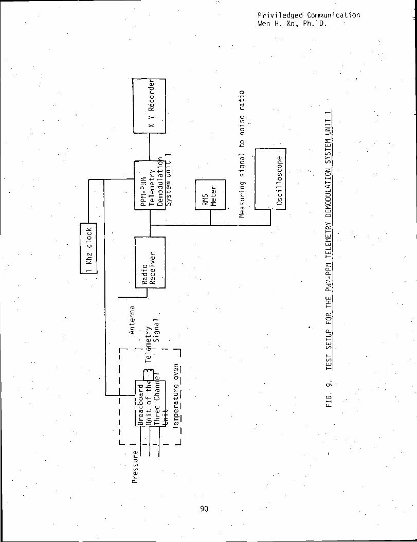
Priviledged CommunicationWen H. Ko, Ph. D.
CDT3S_ooCD
S- roEl -»-> r-3 OJ 13D- E "OI CD O
•^ i— EO- CD CDex i— o
uooNl
CD
QJto
Oco
(T3c:en
•r—l/l
CD
si13
CDQ.Ou
ol/lo
oo>-oo
O2:UJQ
S_CD>
O T-
•r- CD-o uro CDD; o:
Q.D_I
D;oLi-
LU
en
CD
90
Priviledged CommunicationWen H. Ko, Ph. D.
The clock for the modulation and demodulation systems is from an
.NE555 timer running at one KHz. An in-house pressure transducer is used
for pressure sensing and a thermistor is used for temperature sensing.
A Kronkit signal generator and an EKG signal generator supply test signal
to test the frequency response of the system and the EKG recognition'
scheme.
Noise was derived from a drill. At one time, a white noise generator
was used; but the drill proved to be a better shot noise source. The out-
put of the receiver was fed into a RMS meter to give a'quantitive measure
of the noise level generated. .
The three channel telemetry modulation unit was housed in a tempera-
ture oven for the calibration of the temperature channel. A water mano-
meter is used to apply pressure transducer.
The output of the EKG channel of the system, when fed with sinusoidal
wave of different frequencies is shown in Figure 10. .Outputs above 80 Hz
begin to show distortion which can be ascribed to the sampling frequency
of the signal. Figure 11 shows the output of the EKG channel of the
system with an EKG input. The EKG signal observed by the. seven segment
display agreed with the signal period.
The implant package was calibrated in the temperature range of 30°Cto 40°C. Within this range, the calibration is accurate up to 1/2°C,
however, beyond this range, the thermistor begins to exhibit nonlinearity.
The pressure channel calibration is accurate only on a short term basis.
Investigation of the pressure transducer indicates that there is a con-
stant drift in the pressure transducer. •
The effectiveness of the system is discriminating environmental shot
noise was investigated. Typical signal input from the radio receiver
with noise is shown in Figure 11. Without the discrimination scheme, the
output of the demodulation unit a substantial amount of noise leaks
through the threshold detector. Nevertheless, with the first two stages,most of the noise is eliminated.
The pulse rate discriminator discriminated signal from noise to
within a certain tolerance of the previous pulse position and shut off
data processing under sudden occurence of noise after the first two stages.
The output is held constant until noise passes away.
91
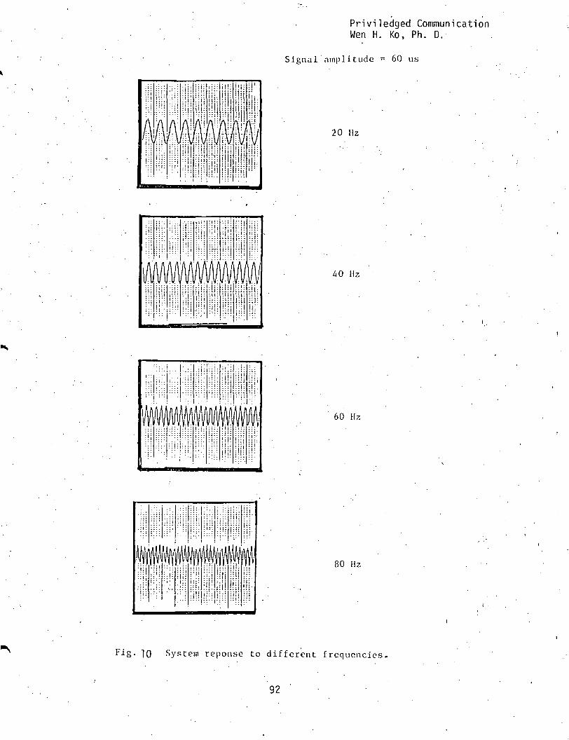
Priviledged CommunicationWen H. Ko, Ph. D.
Signal amplitude = 60 us
20 Hz
40 Hz
60 Hz
80 Hz
]rig- 10 System reponse to different frequencies.
92
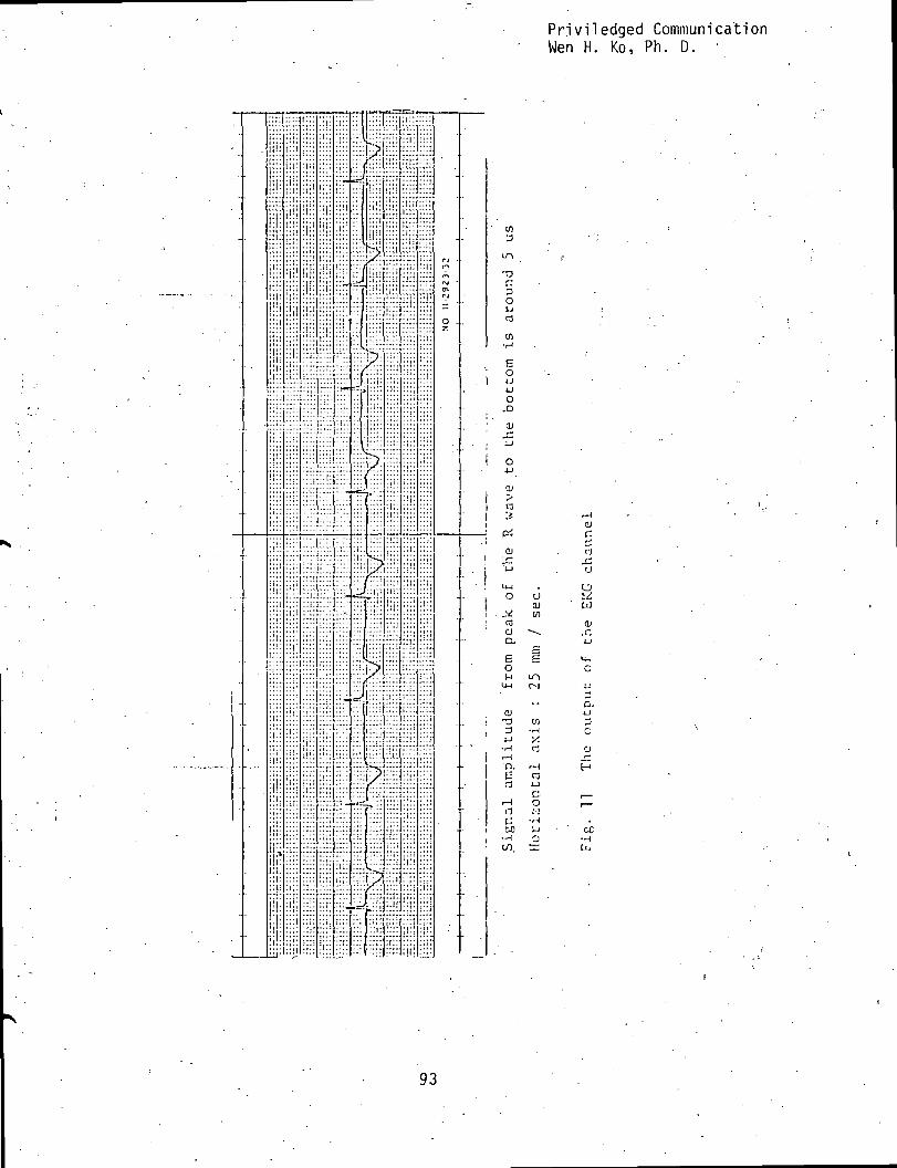
Priviledged CommunicationWen H. Ko, Ph. D. •
III
i I !
I H :1 iI
I I
'•'
1
J
1
I
1
I1I
1
1
I
t1t
1
1'
1
1
f1
1
jl
1|
11
„
1
1 '
I
„
!
1
I
-
1
"
1
II
I
III
1
1
1
"'
I
"
IN -m
n
rj
O .7.
-
-
I
1
'•
!
103
•OC3O
l/>• H
OiJUO
O4-1
CJ
n
u0)c/i
GJc.
eoM
3 -^
•r-l H
^sD. rH
6 an u
c•-H ort MC -HCD i-4
—i aen s:
0)cno
w
j;
DD-
3C
tcu,
93

Priviledged Communication.Wen H. Ko, Ph. D.
PUBLICATION AND THESIS'LIST
Ahn, B.K.; Liu, C.C. and Wist, A.O., "Development of a MiniaturepH Glass Electrode with Field Effect Transistor Amplifierfor Biomedical Application," Medical and Biological Engineer- .ing, May, 1975. • .
Ko, W.H.; Liang, S.P.; and Fung, C., "Design of the PR PoweredCoils for Implant Instruments," submitted to Medical andBiological Engineering, 1977; . . /
Ko, W.H.; Hynecek, J.; and Homa, J., "Single Frequency RF.Power-.ed ECG Telemetry System," submitted to IEEE Trans. BME,' 1977.
Liu, C.C.; Ahn, B.K.; and Brown, E.G., "Engineering Developmentand Evaluation of Implantable pO^, pH, pCC^ Sensors, " 1stPacific Chemical Engineering Congress, Kyoto, Japan, October,1972.
Kp, W.H.; Hynecek, J.; Poon, C.W.; and Greenstein, E., "IngestibleTelemetry System for Low Frequency Signals," 26th ACEMB, Min-neapolis, Minn., October 1973.
Vamvakas, S., "Miniature Three Channel Tape System for Physiolo-' 'gical Monitoring," 10th Annual Meeting of the Association . ,for the Advancement of Medical Instrumentation, Boston, Mass.,March, 1975.
Hynecek, J. and Ko, W.H., "Single Frequency RF Powered TelemetrySystem," 28th ACEMB, New Orleans, Louisiana, September 20-24, .1975.
Ko, W.H.; Hynecek, J.; and Kou, A., "An Implantable Single Fre-quency RF Powered Telemetry System," 3rd InternationalSymposium on Biotelemetry, May 17-20, 1976.
Ko, W.H. and Kou, A., "A Single Frequency RF Powered ImplantableMultichannel Telemetry System in Cardiovascular Application,"29th ACEMB. Boston. Mass., November 6-10, 1976.
Ko, W.H. and Liang, S.P., "RF Powered Cage System for ImplantTelemetry," submitted to the 30th ACEMB, 1977.
Vamvakas, Spiro. Miniature Three channel Tape System for,'Physiological Monitoring, M.S., August, 1974.
Poon, Chie Wan1. An Ingestible Temperature Telemetry System, M.S.,September, 1974.
Todd, Steven Gerald. The Control and Demodulation for a Single >Channel R. F. Powered Telemetry Transmitter, M.S., January, '
-. 1975.
Kou, Abraham. A Single Frequency EF Powered Three Channel Tele-metry System, M.S., June, 1976.
Yau, K.K. A Microprocessor Based Telemetry Demodulation Systemfor Pm/PPM .Telemetry Signals, M.S., June, 1977.
94


![The Value 1 Problem for Probabilistic Automata - LIAFAA characterization 20 fA∗ is the space of prostochastic words. A∗ = fA∗[0] ( fA∗[1] ( fA∗[2] ( ··· ( fA∗. Lemma](https://img.dokumen.tips/doc/110x75/60bb28a9a2770504c97cb50e/the-value-1-problem-for-probabilistic-automata-liafa-a-characterization-20-faa.jpg)