Embed Size (px)
Citation preview

IMPROVEMENTS TOFIELD-PROGRAMMABLE GATE ARRAY DESIGN
EFFICIENCY USINGLOGIC SYNTHESIS
by
Andrew C. Ling
A thesis submitted in conformity with the requirementsfor the degree of Doctor of Philosophy in Engineering
Graduate Department of Electrical and Computer EngineeringUniversity of Toronto
c© Copyright by Andrew C. Ling 2009

IMPROVEMENTS TOFIELD-PROGRAMMABLE GATE ARRAY DESIGNEFFICIENCY USINGLOGIC SYNTHESIS
Andrew C. Ling
Doctor of Philosophy, 2009
Graduate Department of Electrical and Computer Engineering
University of Toronto
Abstract
As Field-Programmable Gate Array (FPGA) capacity can now support several processors
on a single device, the scalability of FPGA design tools and methods has emerged as a
major obstacle for the wider use of FPGAs. For example, logicsynthesis, which has tradi-
tionally been the fastest step in the FPGA Computer-Aided Design (CAD) flow, now takes
several hours to complete in a typical FPGA compile. In this work, we address this problem
by focusing on two areas. First, we revisit FPGA logic synthesis and attempt to improve its
scalability. Specifically, we look at a binary decision diagram (BDD) based logic synthesis
flow, referred to asFBDD, where we improve its runtime by several fold with a marginal
impact to the resulting circuit area. We do so by speeding up the classical cut genera-
tion problem by an order-of-magnitude which enables its application directly at the logic
synthesis level. Following this, we introduce a guided partitioning technique using a fast
global budgeting formulation, which enables us to optimizeindividual “pockets” within the
circuit without degrading the overall circuit performance. By using partitioning we can sig-
nificantly reduce the solution space of the logic synthesis problem and, furthermore, open
up the possibility of parallelizing the logic synthesis step.
ii

The second area we look at is the area of Engineering Change Orders (ECOs). ECOs
are incremental modifications to a design late in the design flow. This is beneficial since
it is minimally disruptive to the existing circuit which preserves much of the engineering
effort invested previously in the design. In a design flow where most of the steps are fully
automated, ECOs still remain largely a manual process. Thiscan often tie up a designer
for weeks leading to missed project deadlines which is very detrimental to products whose
life-cycle can span only a few months. As a solution to this, we show how we can leverage
existing logic synthesis techniques to automatically modify a circuit in a minimally disrup-
tive manner. This can significantly reduce the turn-around time when applying ECOs.
iii

Acknowledgments
I would like to gratefully acknowledge the enthusiastic supervision of my advisors Pro-
fessor Jianwen Zhu and Professor Stephen D. Brown for their continuous guidance and
inspiration. Their technical leadership and coaching ability is something I aspire to achieve
and their influence has made me into a better research scientist, mentor, and person.
I would also like to thank Professor Andreas Veneris and Professor Zvonko Vranesic for
their guidance throughout this process. They have always shown interest in my develop-
ment and are always there to lend some advice when it is needed. They have definitely
contributed to the completion and success of this dissertation and my development.
I would like to thank Dr. Sean Safarpour and Terry Yang for their friendship and fruitful
discussions; particularly for the work presented in Chapter 5 of this dissertation. They have
always made time to meet me which has often led to several insights discussed in this work.
I would like to thank Dr. Tomasz Czakwoski, Rami Beidas, and Franjo Plavec for the
many years of constructive criticisms they have provided. Through their feedback, this
work has definitely been made stronger.
I would like to acknowledge the friends I have made during this process from the LP392
and SF2206 labs (Jason Luu, Navid Toosizadeh, Nahi Abdul Ghani, Dr. Ian Kwon, Sari
Onaissi, Dr. Imad Ferzli, Dr. Peter Yiannacouras, Khaled Heloue, Ivan Matosevic, Davor
Capalija, Cedomir Segulja, and Ahmed Abdelkhalek). They have always kept the boredom
away and have been a great support in this phase of my life.
I would like to thank my parents for their continued guidanceand advice throughout the
years, who have always been there for me, far beyond the last few years of my life.
Finally, I would like to thank my wife, Julie Sit, for being there with me during this
journey. You are my best friend and companion, and I would notbe the same without you.
iv

Contents
List of Figures viii
List of Tables xii
1 Introduction 11.1 Introduction to Field-Programmable Gate Arrays . . . . . .. . . . . . . . 11.2 Motivation and Overview . . . . . . . . . . . . . . . . . . . . . . . . . . .21.3 Objective and Contributions . . . . . . . . . . . . . . . . . . . . . . .. . 61.4 Dissertation Organization . . . . . . . . . . . . . . . . . . . . . . . .. . . 7
2 Background 82.1 Terminology . . . . . . . . . . . . . . . . . . . . . . . . . . . . . . . . . . 82.2 Field-Programmable Gate Array (FPGA) Architecture . . .. . . . . . . . 10
2.2.1 Programmable Logic . . . . . . . . . . . . . . . . . . . . . . . . . 102.2.2 Commercial Architectures . . . . . . . . . . . . . . . . . . . . . . 12
2.3 FPGA Computer-Aided Design (CAD) . . . . . . . . . . . . . . . . . . .. 132.3.1 Logic Synthesis and Technology Mapping . . . . . . . . . . . .. . 142.3.2 Clustering, Placement, and Routing . . . . . . . . . . . . . . .. . 172.3.3 Physically-Driven Synthesis . . . . . . . . . . . . . . . . . . . .. 192.3.4 Engineering Change Orders (ECOs) . . . . . . . . . . . . . . . . .192.3.5 Timing Analysis . . . . . . . . . . . . . . . . . . . . . . . . . . . 21
2.4 Introduction to Binary Decision Diagrams . . . . . . . . . . . .. . . . . . 242.4.1 Zero-Suppressed Binary Decision Diagrams . . . . . . . . .. . . . 31
2.5 Introduction to Boolean Satisfiability . . . . . . . . . . . . . .. . . . . . . 322.6 Solving the Boolean Satisfiability Problem . . . . . . . . . . .. . . . . . . 34
2.6.1 Heuristics To Solve the Boolean Satisfiability Problem . . . . . . . 362.6.2 Circuits and Boolean Satisfiability . . . . . . . . . . . . . . .. . . 39
2.7 Relationship between Binary Decision Diagrams and Boolean Satisfiability 432.8 Summary . . . . . . . . . . . . . . . . . . . . . . . . . . . . . . . . . . . 44
3 Improving BDD-based Logic Synthesis through Elimination and Cut-Compression 453.1 Introduction to Logic Synthesis . . . . . . . . . . . . . . . . . . . .. . . . 463.2 Motivation . . . . . . . . . . . . . . . . . . . . . . . . . . . . . . . . . . . 463.3 Adaptation of Covering Problem to Elimination . . . . . . . .. . . . . . . 50
3.3.1 Covering Problem . . . . . . . . . . . . . . . . . . . . . . . . . . 503.3.2 Binary Decision Diagram (BDD)-based Cut-Compression . . . . . 54
v

Contents
3.3.3 Symbolic Cut Generation Algorithm . . . . . . . . . . . . . . . .. 603.3.4 EnsuringK-Feasibility . . . . . . . . . . . . . . . . . . . . . . . . 613.3.5 Finding the Minimum Cost Cut . . . . . . . . . . . . . . . . . . . 633.3.6 Using Zero-Suppressed Binary Decision Diagrams (ZDDs) . . . . . 653.3.7 Reconvergence and Edge-Flow . . . . . . . . . . . . . . . . . . . . 65
3.4 Results . . . . . . . . . . . . . . . . . . . . . . . . . . . . . . . . . . . . . 683.4.1 BddCut: Scalable Cut Generation . . . . . . . . . . . . . . . . . .683.4.2 Edge Flow Heuristic . . . . . . . . . . . . . . . . . . . . . . . . . 723.4.3 Covering based Elimination . . . . . . . . . . . . . . . . . . . . . 733.4.4 Comparison with Structural Synthesis . . . . . . . . . . . . .. . . 75
3.5 Summary . . . . . . . . . . . . . . . . . . . . . . . . . . . . . . . . . . . 77
4 Budget Management for Partitioning 784.1 Background and Previous Work . . . . . . . . . . . . . . . . . . . . . . .83
4.1.1 Budget Management . . . . . . . . . . . . . . . . . . . . . . . . . 834.2 Partitioning with Delay Budgeting . . . . . . . . . . . . . . . . . .. . . . 85
4.2.1 Partitioning and And-Inverter Graph (AIG) construction . . . . . . 864.2.2 Budget Management . . . . . . . . . . . . . . . . . . . . . . . . . 874.2.3 Resynthesis with Delay Budgets . . . . . . . . . . . . . . . . . . 107
4.3 Results . . . . . . . . . . . . . . . . . . . . . . . . . . . . . . . . . . . . . 1074.3.1 Dual Problem Performance . . . . . . . . . . . . . . . . . . . . . . 1084.3.2 Budget Management for Partitioned Logic Synthesis . .. . . . . . 109
4.4 Summary . . . . . . . . . . . . . . . . . . . . . . . . . . . . . . . . . . . 111
5 Automation of ECOs 1125.1 Background and Related Work . . . . . . . . . . . . . . . . . . . . . . . .115
5.1.1 Terminology . . . . . . . . . . . . . . . . . . . . . . . . . . . . . 1155.1.2 Related Work . . . . . . . . . . . . . . . . . . . . . . . . . . . . . 1155.1.3 Boolean Satisfiability (SAT) . . . . . . . . . . . . . . . . . . . . .116
5.2 Automated ECOs: General Technique . . . . . . . . . . . . . . . . . .. . 1185.2.1 Netlist Localization . . . . . . . . . . . . . . . . . . . . . . . . . . 1205.2.2 Netlist Modification . . . . . . . . . . . . . . . . . . . . . . . . . 122
5.3 Results . . . . . . . . . . . . . . . . . . . . . . . . . . . . . . . . . . . . . 1365.3.1 Specification Changes . . . . . . . . . . . . . . . . . . . . . . . . 1375.3.2 Error Correction . . . . . . . . . . . . . . . . . . . . . . . . . . . 1405.3.3 Generation of Model Netlist . . . . . . . . . . . . . . . . . . . . . 143
5.4 Summary . . . . . . . . . . . . . . . . . . . . . . . . . . . . . . . . . . . 144
6 Conclusion and Future Work 1456.1 Summary of Contributions . . . . . . . . . . . . . . . . . . . . . . . . . .1456.2 Future Work . . . . . . . . . . . . . . . . . . . . . . . . . . . . . . . . . . 146
7 Appendix: ZDD Prune Algorithm 149
vi

Contents
References 152
vii

List of Figures
1.1 A traditional island-style FPGA architecture. . . . . . . .. . . . . . . . . 11.2 Initial costs for fabricating an Application-Specific Integrated Circuit (ASIC)
as measured by the mask set costs for each technology node from 1994 to2007[Yan01, RMM+03, Lam05]. . . . . . . . . . . . . . . . . . . . . . . . 2
1.3 A normalized cost comparison between a Xilinx FPGA versus a Texas In-struments Digital Signal Processing/Processor (DSP)[Alt05a, Bie07]. . . . 3
2.1 A Basic Logic Element (BLE) consisting of a Lookup Table (LUT) and aconfigurable register. . . . . . . . . . . . . . . . . . . . . . . . . . . . . . 11
2.2 The hierarchical structure of an FPGA. . . . . . . . . . . . . . . .. . . . . 122.3 Altera’s Stratix commercial FPGA [LBJ+03]. . . . . . . . . . . . . . . . . 132.4 A multiply-accumulate “hard” block on the commercial Stratix FPGA [Alt05b]. 142.5 A generic CAD flow for FPGAs. . . . . . . . . . . . . . . . . . . . . . . . 152.6 An illustration of the logic synthesis process and technology mapping. (a)
An unoptimized netlist. (b) An optimized netlist. (c) Identification of nodesto pack into a LUT for technology mapping. (d) Technology mapped circuitto 4-input LUTs. . . . . . . . . . . . . . . . . . . . . . . . . . . . . . . . 16
2.7 The half-perimeter wirelength of a net is defined as half of the rectangleperimeter which encompasses all terminals of the net. This rectangle istermed as abounding box. . . . . . . . . . . . . . . . . . . . . . . . . . . 18
2.8 Illustration of physically-driven synthesis applyingretiming. (a) Currentplacement with long distance between register d and logic element c. (b)Post-placement layout-driven optimization using retiming. (c) Incrementalplacement process for legalization. (d) Final legal placement of optimizednetlist. . . . . . . . . . . . . . . . . . . . . . . . . . . . . . . . . . . . . . 20
2.9 An illustration of a circuit graph with static timing values assigned to eachnode and edge. . . . . . . . . . . . . . . . . . . . . . . . . . . . . . . . . 22
2.10 Graphical representation of Shannon’s expansion. . . .. . . . . . . . . . . 252.11 Truth-table, cube, and Binary Decision Diagram (BDD) representation of
functionf = x1x3x4 + x1x2x3 + x1x2x4. . . . . . . . . . . . . . . . . . . 262.12 An illustration of reduction rule 1: removing redundant assignments. . . . . 272.13 An illustration applying reduction rule 1 to the entiregraph: removing all
redundant assignments. . . . . . . . . . . . . . . . . . . . . . . . . . . . . 282.14 An illustration of reduction rule 2: removing duplicate nodes. . . . . . . . . 292.15 An illustration of using inverted edges. . . . . . . . . . . . .. . . . . . . . 302.16 An illustration of two resulting BDDs if alternate variable orders are used. . 31
viii
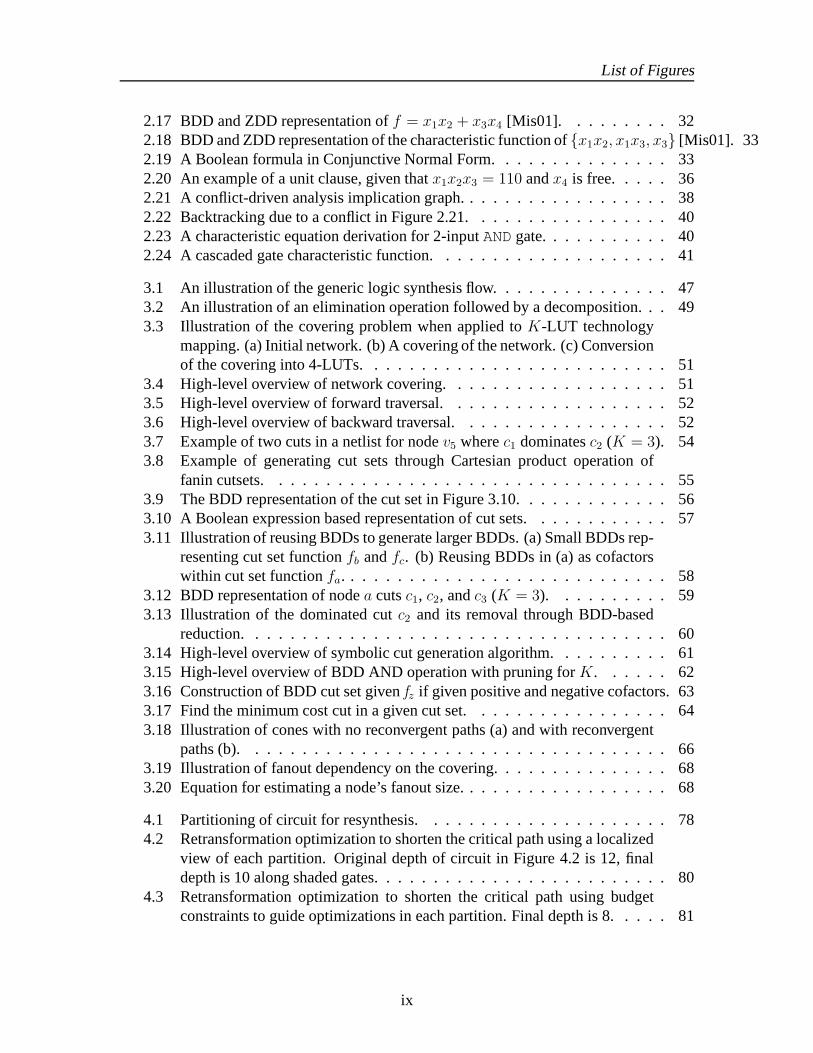
List of Figures
2.17 BDD and ZDD representation off = x1x2 + x3x4 [Mis01]. . . . . . . . . 322.18 BDD and ZDD representation of the characteristic function of{x1x2, x1x3, x3} [Mis01]. 332.19 A Boolean formula in Conjunctive Normal Form. . . . . . . . .. . . . . . 332.20 An example of a unit clause, given thatx1x2x3 = 110 andx4 is free. . . . . 362.21 A conflict-driven analysis implication graph. . . . . . . .. . . . . . . . . . 382.22 Backtracking due to a conflict in Figure 2.21. . . . . . . . . .. . . . . . . 402.23 A characteristic equation derivation for 2-inputANDgate. . . . . . . . . . . 402.24 A cascaded gate characteristic function. . . . . . . . . . . .. . . . . . . . 41
3.1 An illustration of the generic logic synthesis flow. . . . .. . . . . . . . . . 473.2 An illustration of an elimination operation followed bya decomposition. . . 493.3 Illustration of the covering problem when applied toK-LUT technology
mapping. (a) Initial network. (b) A covering of the network.(c) Conversionof the covering into 4-LUTs. . . . . . . . . . . . . . . . . . . . . . . . . . 51
3.4 High-level overview of network covering. . . . . . . . . . . . .. . . . . . 513.5 High-level overview of forward traversal. . . . . . . . . . . .. . . . . . . 523.6 High-level overview of backward traversal. . . . . . . . . . .. . . . . . . 523.7 Example of two cuts in a netlist for nodev5 wherec1 dominatesc2 (K = 3). 543.8 Example of generating cut sets through Cartesian product operation of
fanin cutsets. . . . . . . . . . . . . . . . . . . . . . . . . . . . . . . . . . 553.9 The BDD representation of the cut set in Figure 3.10. . . . .. . . . . . . . 563.10 A Boolean expression based representation of cut sets.. . . . . . . . . . . 573.11 Illustration of reusing BDDs to generate larger BDDs. (a) Small BDDs rep-
resenting cut set functionfb andfc. (b) Reusing BDDs in (a) as cofactorswithin cut set functionfa. . . . . . . . . . . . . . . . . . . . . . . . . . . . 58
3.12 BDD representation of nodea cutsc1, c2, andc3 (K = 3). . . . . . . . . . 593.13 Illustration of the dominated cutc2 and its removal through BDD-based
reduction. . . . . . . . . . . . . . . . . . . . . . . . . . . . . . . . . . . . 603.14 High-level overview of symbolic cut generation algorithm. . . . . . . . . . 613.15 High-level overview of BDD AND operation with pruning for K. . . . . . 623.16 Construction of BDD cut set givenfz if given positive and negative cofactors. 633.17 Find the minimum cost cut in a given cut set. . . . . . . . . . . .. . . . . 643.18 Illustration of cones with no reconvergent paths (a) and with reconvergent
paths (b). . . . . . . . . . . . . . . . . . . . . . . . . . . . . . . . . . . . 663.19 Illustration of fanout dependency on the covering. . . .. . . . . . . . . . . 683.20 Equation for estimating a node’s fanout size. . . . . . . . .. . . . . . . . . 68
4.1 Partitioning of circuit for resynthesis. . . . . . . . . . . . .. . . . . . . . 784.2 Retransformation optimization to shorten the criticalpath using a localized
view of each partition. Original depth of circuit in Figure 4.2 is 12, finaldepth is 10 along shaded gates. . . . . . . . . . . . . . . . . . . . . . . . . 80
4.3 Retransformation optimization to shorten the criticalpath using budgetconstraints to guide optimizations in each partition. Final depth is 8. . . . . 81
ix

List of Figures
4.4 Illustration of numericdepth budgetassignments to each partition input. . . 824.5 Alternate implementations of the same circuit, each node with a different
circuit latency allocated to it. . . . . . . . . . . . . . . . . . . . . . . .. . 854.6 Clustering of a simple netlist. (a) Original netlist (b)Partitioning of original
netlist (c) Representing each partition and PI as a single node . . . . . . . . 874.7 Example of an And-Inverter Graph (AIG) where each node isa 2-input
ANDgate and each edge can be inverted. . . . . . . . . . . . . . . . . . . . 874.8 Illustration of circuit optimization for 4.8(a) area (gate-count=4, logic-levels=4)
and 4.8(b) depth (gate-count=7, logic-levels=3). . . . . . . .. . . . . . . . 884.9 Annotated partition inputs after delay budgeting. . . . .. . . . . . . . . . 894.10 Simplified inverse relationship between delay budget,bij , and area estima-
tion,Fij(bij), defined over variablebij . . . . . . . . . . . . . . . . . . . . . 904.11 Graph to ILP formulation. . . . . . . . . . . . . . . . . . . . . . . . . .. 924.12 Illustration of dependency of depth between inputs. . .. . . . . . . . . . . 924.13 Graphical illustration of transforming the budget management problem into
its dual network flow problem. (a) Partitioned graph. (b) Upper and lowerbound added as edges to create network flow graph. . . . . . . . . . .. . 100
4.14 Illustration of proof for Proposition 4.2.3. (a) TotalcostM = −Lij ×ρij + Uij × λij . (b) Alternate feasible flow that does not violate the flowconservation of nodei or j. Total costM ′ = −Lij × (ρij − 1) + Uij ×(λij − 1) = M + Lij − Uij , sinceLij < Uij thenM ′ < M . . . . . . . . . 102
4.15 Graphical illustration of findinga∗i values from the residual network flow
graph. (a) Dual network flow graph. (b) Residual graph formedafter solv-ing dual problem. (c)a∗
i values found for each nodei along with resultingbij values for each input edge. . . . . . . . . . . . . . . . . . . . . . . . . 103
4.16 Illustration of area penalty with depth reduction and inverted edges. . . . . 1044.17 Illustration of how reducing the depth of a path impactsdecisions along
other paths and partitions. . . . . . . . . . . . . . . . . . . . . . . . . . . .1054.18 Illustration of area-depth relationship for functionF (bij). . . . . . . . . . . 1064.19 Depth assignments to inputs after delay budget assignments. (a) Delay
budgets assigned to each partition input. (b) Depth adjustment found fromEquation 4.18. Assignments to each partition input are usedto drive theresynthesis engine. . . . . . . . . . . . . . . . . . . . . . . . . . . . . . . 108
5.1 Generalized flow using ECOs. . . . . . . . . . . . . . . . . . . . . . . . .1135.2 Characteristic function derivation for 2-input AND gate. . . . . . . . . . . 1175.3 Cascaded gate characteristic function: top clauses from ANDgate; bottom
clauses fromORgate. . . . . . . . . . . . . . . . . . . . . . . . . . . . . . 1185.4 Automated ECO flow: a MAX-SAT based netlist localizationstep followed
by a SAT based Netlist Modification step. . . . . . . . . . . . . . . . . .. 1195.5 Maximum satisfiability solution to localization. . . . . .. . . . . . . . . . 1205.6 Illustration of localized nodeξ. Modification can be applied by replacing
H(Xp) with some arbitrary functionFc(Xs). . . . . . . . . . . . . . . . . . 123
x

List of Figures
5.7 Circuit to be modified . . . . . . . . . . . . . . . . . . . . . . . . . . . . . 1255.8 Functional dependency example . . . . . . . . . . . . . . . . . . . . .. . 1285.9 Deriving global functionF = h(g1, g2) using dependency check construct. . 1295.10 Searching for basis functions flow. . . . . . . . . . . . . . . . . .. . . . . 1325.11 Random simulation example.. . . . . . . . . . . . . . . . . . . . . . . . . . 1335.12 Circuit reduction. . . . . . . . . . . . . . . . . . . . . . . . . . . . . . .. 1355.13 Example changes in HDL code. . . . . . . . . . . . . . . . . . . . . . . .1385.14 Impact of output removal on SAT solver runtime for circuit b15 . . . . . . . 143
7.1 High-level overview of ZDD Unate Product operation withpruning forK. . 1507.2 Illustration of dominated cut removal in BDD versus ZDD.. . . . . . . . . 1517.3 Larger example of illustration of dominated cut removalin BDD versus
ZDD. Picture taken from the CUDD BDD/ZDD package [Som98]. . .. . . 151
xi

List of Tables
2.1 Conversion rules for CNF Construction. . . . . . . . . . . . . . .. . . . . 342.2 Characteristic functions for basic logic elements [Smi04, ch.2]. . . . . . . . 42
3.1 Detailed comparison of BddCut cut generation time against IMap and ABC.IMap could not run forK ≥ 8. . . . . . . . . . . . . . . . . . . . . . . . . 69
3.2 Detailed comparison of BddCut cut generation time against ABC forK ≥ 8. 703.3 Average ratio of IMap
BddCutcut generation times. IMap could not be run for
K ≥ 8. . . . . . . . . . . . . . . . . . . . . . . . . . . . . . . . . . . . . 703.4 Average ratio of ABC
BddCutcut generation times. . . . . . . . . . . . . . . . . 70
3.5 Average ratio of ABCBddCut
memory usage. . . . . . . . . . . . . . . . . . . . 703.6 Runtime comparison of BddCut with ABC on circuitleon2 (contains
278,292 4-LUTs). . . . . . . . . . . . . . . . . . . . . . . . . . . . . . . . 713.7 FPGA channel-width reduction using EdgeFlow with Cut-Height (Delay
values in nanoseconds). . . . . . . . . . . . . . . . . . . . . . . . . . . . . 733.8 Detailed comparison of area and runtime ofFBDDnew against FBDD and
SIS forK = 8. FBDDnew
FBDD or SIS. . . . . . . . . . . . . . . . . . . . . . . . . . 74
3.9 Comparison of area and runtime of FBDD againstFBDDnew for variousvalues ofK, FBDD
FBDDnew
. . . . . . . . . . . . . . . . . . . . . . . . . . . . . 753.10 Comparison of area and runtime of FBDD (K = 8) against AIG Rewrit-
ing/Refactoring. . . . . . . . . . . . . . . . . . . . . . . . . . . . . . . . . 76
4.1 Infimum of several functions . . . . . . . . . . . . . . . . . . . . . . . .. 974.2 Runtime comparison of ILP and NF formulation, over 100 circuits ran,
only largest circuits shown. Run on a Pentium 4, 2.80GHz with2GB of RAM1094.3 Impact of budget management framework on area and depth for the IWLS
set, only larger circuits shown in detail. . . . . . . . . . . . . . . .. . . . 110
5.1 Impact of modifications on circuit performance on a Stratix chip. . . . . . 1385.2 Automated correction results on a Stratix chip. . . . . . . .. . . . . . . . . 141
xii

List of Acronyms
AIG And-Inverter Graph
ASIC Application-Specific Integrated Circuit
BDD Binary Decision Diagram
BLE Basic Logic Element
CAD Computer-Aided Design
CLB Clustered Logic Block
CNF Conjunctive Normal Form
DAG Directed Acyclic Graph
DSP Digital Signal Processing/Processor
ECO Engineering Change Order
EDA Electronic-Design Automation
FPGA Field-Programmable Gate Array
GPU Graphical Processing Unit
HDL Hardware Description Language
HPC High-Performance Computing
ILP Integer-Linear Program
IWLS International Workshop on Logic and Synthesis
LAB Logic-Array Block
LUT Lookup Table
MAX-SAT Maximum Boolean Satisfiability
QoR Quality of Result
ROBDD Reduced Ordered Binary Decision Diagram
xiii

List of Acronyms
SAT Boolean Satisfiability
SOP Sum of Products
SOPC System on Programmable Chip
ZDD Zero-Suppressed Binary Decision Diagram
xiv

1 Introduction
1.1 Introduction to Field-Programmable Gate Arrays
Since their introduction in 1985, Field-Programmable GateArrays (FPGAs) have become
an effective medium to quickly implement a wide range of digital applications. An FPGA
is a regular array of programmable logic and routing structures, as illustrated in Figure 1.1.
Digital logic is implemented on an FPGA by programming theirlogic blocks and routing
fabric to various configurations.
������
�������� ����
�������������
��� �������� ����� ����� �����
� ��� ������
� �������������� ����� ��� ��� �����
��!"""#$��� ���
� ����� ������ � �������� %� ���
�&�����������'(�����)����� � ��*���+ �����
)����� � ��,��������������������)����� � ��-����������
Figure 1.1: A traditional island-style FPGA architecture.
1

1 Introduction
1.2 Motivation and Overview
The programmable nature of FPGAs make them an extremely cost-effective solution for
designing digital applications. For example, for a few thousand dollars, one can purchase
an FPGA to implement an entire System on Programmable Chip (SOPC) [ter09]. Contrast
this to the initial development and fabrication costs for anASIC which currently costs
upwards of a million dollars [ICK04, Lam03]. As this trend has worsened over time, as
shown in Figure 1.2, it is expected that FPGA use over ASICs will grow.
0.5u 0.35u 0.25u 0.18u 0.13u 0.09u 0.065u$0.0
$0.5M
$1.0M
$1.5M
$2.0M
$2.5M
$3.0M
$3.5M
AS
IC M
ask
Set
Cos
ts (
US
D)
1994 1995 1998 1999 2000 2002 2007Technology Node and Year
Figure 1.2: Initial costs for fabricating an ASIC as measured by the mask set costs for eachtechnology node from 1994 to 2007[Yan01, RMM+03, Lam05].
The cost advantage of FPGAs, however, comes with a penalty interms of circuit area,
power, and performance. Fortunately, a large body of work inthe last 20 years has signifi-
cantly improved both the costs and performance of FPGAs. These can be broken down
into architectural enhancements, which explore programmable fabric improvements on
2

1 Introduction
the FPGA [WRV96, RBM99, AR00, LBJ+03, LAB+05, Mor06b]; and CAD enhance-
ments, which explore algorithms that map digital applications onto the programmable
fabric [BRV90, ME95, BR97b, BR97a, MBR99, LSB05b, MSB05, SMB05a, MBV06,
MCB06a, MCB06b]. As a result of these improvements, FPGA costs and performance
have improved by several fold. Furthermore, in several application domains FPGAs have a
significant cost and performance advantage. For example, Figure 1.3 illustrates the costs,
measured in terms of silicon area, of an FPGA and DSP implementation of a well known
DSP application1. This clearly shows that for equal performance, the FPGA is an order-
of-magnitudecheaper than the DSP [Alt05a, Bie07]. However, even with these compelling
advantages of FPGAs, they currently take upless than 2%of the semiconductor mar-
ket [McM08, Wor06].
0
10
20
30
40
Cos
t Per
Ope
ratio
n(n
orm
aliz
ed to
Xili
nx F
PG
A)
Xilinx TI Virtex−4 TMS320C6410
SX25 400 MHz
Figure 1.3: A normalized cost comparison between a Xilinx FPGA versus a Texas Instru-ments DSP[Alt05a, Bie07].
One reason that FPGA growth has been limited is due to the cumbersome nature and
high-learning curve of the FPGA design flow. The FPGA CAD flow has generally been
1The DSP application was an orthogonal frequency-division multiplexing (OFDM) unit, each operation isdefined as the computation required to process a single channel [Alt05a, Bie07].
3

1 Introduction
adopted from the ASIC domain, and as a result, FPGA CAD flows suffer from scalability
problems typically found in by ASIC CAD tools. In particular, the compile time of the en-
tire FPGA CAD flow commonly takes on the order of hours to complete. Compare this to
the typical compile times for DSPs or software approaches which take on the order of min-
utes to complete. A second issue is that manual interventionis often required by the user
to alter the design and meet constraints: something that requires extensive knowledge of
hardware design and the underlying FPGA architecture. Boththese factors significantly de-
grade FPGA design productivity, which deters new entrants from using FPGAs to leverage
their benefits; particularly those who are unfamiliar with the digital design flow. This dis-
sertation attempts to address this issue by focusing on two areas. First, we demonstrate how
we can improve the productivity of the FPGA CAD flow by reducing its runtime through
several fast global optimization techniques. Second, we remove the manual nature of the
backend FPGA CAD flow. Improvements to both of these areas would not only reduce the
learning curve of using FPGAs to encourage wider use of FPGAs, but also enhance the
FPGA design experience for the large number of existing FPGAusers.
To reduce the runtime of the FPGA CAD flow, we focus on logic synthesis. Logic syn-
thesis has a large impact on the final implementation of a circuit and remains an important
problem in the FPGA CAD flow. Furthermore, it occupies a significant portion of runtime
in a circuit compile2. In this dissertation, we will look at a synthesis flow that leverages
Binary Decision Diagrams (BDDs). BDD-based synthesis flowsare a powerful means to
optimize a circuit for area, power, and delay [YCS00, VKT02,MSB05]. However, one of
the primary bottlenecks in BDD-based synthesis flows is their clustering and elimination
step. During elimination, redundancies in the circuit are removed and resynthesis regions
are defined. Current methods for elimination accomplish these tasks through trial-and-
error and, hence, will not scale to modern designs containing hundreds of thousands of
2Commercial numbers have not been publicly disclosed by informally have listed anywhere from 30 to 50%of the overall CAD runtime [Alt07, Xil00].
4

1 Introduction
logic blocks. This issue could be solved by treating elimination as a covering problem.
Doing so would convert the elimination problem to an extremely fast global optimization
problem rather than a greedy-based heuristic. In order to ensure that the covering prob-
lem scales to elimination, we introduce a novel compressiontechnique using BDDs to help
compress the cuts necessary when solving the covering problem. This ultimately leads to
an order-of-magnitude speedup in the cut generation process and a several fold speedup in
the overall synthesis flow with negligible impact on circuitarea.
Another technique to improve the runtime of CAD is through partitioning for paralleliza-
tion on multi-core processors. During partitioning, a circuit is split into several independent
subcircuits where each subcircuit is optimized individually. Although this can significantly
reduce the runtime of the optimization process, each partition only provides a localized
view of the entire circuit and, as a result, optimizing each partition does not guarantee a sat-
isfactory global result. As a solution to this, we formulatean Integer-Linear Program (ILP)
that derives partition constraints during optimization. By following these constraints, the
localized optimizer will produce a solution with superior quality to that of one with only
a localized view of the partition. Unfortunately, our ILP formulation is NP-complete and
does not scale to large circuits. To avoid this issue, we showhow we can reduce our ILP to
polynomial complexity by leveraging the concept of duality. Doing so improves the prob-
lem runtime by over 100x. Furthermore, although our reducedproblem theoretically has a
polynomial complexity with respect to circuit size, empirically we find that it runs in linear
time on average. When run on the IWLS benchmark set (the largest academic benchmark
set used in logic synthesis), we show that our ILP formulation can improve circuit depth by
11% on average when compared against partitioning-based flows that do not use our tech-
nique. Furthermore, our reduction in depth comes with a lessthan 1% penalty to circuit
area.
Finally, in an effort to improve the FPGA design flow, we investigate ECOs. ECOs are
5

1 Introduction
an essential methodology to apply late-stage specificationchanges and bug fixes. ECOs
are beneficial since they are applied directly to a place-and-routed netlist which preserves
most of the engineering effort invested previously. In a design flow where almost all tasks
are automated, ECOs remain a primarily manual and expensiveprocess. As a solution, we
introduce an automated method to tackle the ECO problem. Specifically, we introduce a
resynthesis technique using Boolean Satisfiability (SAT) which can automatically update
the functionality of a circuit by leveraging the existing logic within the design; thereby
removing the inefficient manual effort required by a designer. By using this technique, we
show how we can automatically update a circuit implemented on an FPGA while keeping
over 90% of the placement unchanged.
1.3 Objective and Contributions
The objective of this research is to enhance the user experience of FPGA design tools
through two goals as follows:
1. Enhancing the scalability to the general logic synthesisflow.
2. Removing the manual nature of ECOs in the FPGA CAD flow.
Achieving these goals led to five primary contributions as follows:
1. A novel BDD-based compression technique for cut generation to reduce its runtime
and memory use by an order of magnitude.
2. A novel edge-flow heuristic that reduces the number of routing wires by 7% when
used during logic synthesis3.
3As technology scales down beyond 65nm, routing wires begin to dominate the overall circuit area, thusreducing routing wires significantly reduces the cost and improves the delay of the circuit [ZLM06].
6

1 Introduction
3. A global covering based approach to solve the eliminationproblem in logic synthesis
reducing the elimination runtime by an order of magnitude reduction.
4. A formulation of the slack-budget management problem as an Integer-Linear Program
followed by a reduction method leveraging duality to reduceour Integer-Linear Program
to a network flow algorithm with polynomial complexity. Thisreduces the slack-
budget management problem runtime by two orders of magnitude on average.
5. An automated approach to the FPGA ECO flow that uses BooleanSatisfiability to
isolate and resynthesize logic.
1.4 Dissertation Organization
The remainder of this dissertation is organized as follows:Chapter 2 gives a brief overview
of FPGA architecture and CAD flow. A brief tutorial on Binary Decision Diagrams (BDDs)
and Boolean Satisfiability (SAT) is also be provided. Chapter 3 introduces our novel ap-
proach to elimination for logic synthesis. We also describehow we use BDDs to signifi-
cantly reduce the memory and computational requirements ofgenerating cuts during elim-
ination. Chapter 4 outlines our slack-budget management formulation as an Integer-Linear
Program and show how it can be used in conjunction with partitioning to improve circuit
depth. Chapter 5 covers our automated approach for ECOs using Boolean Satisfiability.
Finally, we conclude in Chapter 6 with a summary and directions for future work.
7

2 Background
This chapter provides a brief overview of FPGA architectureand CAD. Also, a descrip-
tion of Binary Decision Diagrams (BDDs) and the Boolean Satisfiability (SAT) problem
is given. Each section is generally self contained, thus, the reader can skip to sections
that they are unfamiliar with to give a better foundation on knowledge when reading the
succeeding chapters in this dissertation.
2.1 Terminology
The following section describes some basic terminology used throughout this dissertation.
The combinational portion of a Boolean circuit can be represented as a directed acyclic
graph (DAG)G = (V (G), E(G)). A node in the graphv ∈ V (G) represents a logic gate,
primary input or primary output, and a directed edge in the graph〈u, v〉 ∈ E(G) represents
a signal in the logic circuit that is an output of gateu and an input of gatev. For a given
edge〈u, v〉, u is known as the tail andv is known as the head. Afaninfor nodev, fanin(v),
is defined as a tail node for an edge with headv. Similarly, afanoutfor nodev is defined as
a head node for an edge with tailv. A primary input(PI) node has no fanins and aprimary
output(PO) node has no fanouts. Aninternal node has both fanins and fanouts. Registers
can be represented in the DAG if the inputs of the registers are modelled as POs and the
outputs of the registers are modelled as PIs. Since registers can form a cycle in a graph,
they should not be treated as nodes, as cycles are very difficult to handle in many circuit
8

2 Background
optimization algorithms.
A nodev is K-feasibleif | fanin(v) |≤ K. If every node in a graph isK-feasible then
the graph isK-bounded. A path, is defined as a sequence of nodes starting at nodes and
ending at nodet such that for each adjacent two nodes,u andv, in a sequence, there exists
a directed edge〈u, v〉 ∈ E(G). For any given path,s is known as a transitive fanin for node
t andt is known as the transitive fanout for nodes. Here, we assume parallel edges do not
exist within the graph, since our definitions of edges and paths cannot disambiguate parallel
edges and paths (e.g. two edges connecting the same sourceu and sinkv). The length of a
path is the sum of the delays of the edges and nodes along the path. If we assume that the
delay of each edge are equal, at a nodev, the depth,depth(v), is the length of the longest
path from a primary input tov and the height,height(v), is the length of the longest path
from v to a primary output. Both the depth for a PI node and the heightfor a PO node are
zero. The depth or height of a graph is the length of the longest path in the graph.
When visiting nodes in the graph, they are often visited intopological order. In topo-
logical order, nodes are visited if and only if all of their fanins have been already visited.
This implies that the node traversal occurs from PIs to POs. Reverse topological order is
the opposite case where nodes are visited if and only if all oftheir fanout nodes have been
visited already.
A coneof v, Cv, is a subgraph consisting ofv and some of its nonPI predecessors such
that any nodeu ∈ Cv has a path tov that lies entirely inCv. Nodev is referred to as the
root of the cone. The size of a cone is the number of nodes plus edgesin the cone. This
parameter often determines the computational complexity of operations on the cone since
many optimization on a cone of logic require traversing all the nodes or edges within the
cone. At a coneCv, the set of fanins,fanin(Cv), are the set of nodes that are the tail nodes
of edges with a head inCv and the set of fanouts,fanout(Cv), are the set of nodes that are
the head nodes of edges withv as a tail. With fanins and fanouts so defined, a cone can
9
2 Background
be viewed as a node, and notions that were previously defined for nodes can be extended
to handle cones. Notions such asdepth( · ), height( · ) andK-feasibility all have similar
meanings for cones as they do for nodes.
A cut of a nodev is the set of fanin nodes to a cone whose root isv. Thus, every cone
defines a cut and there is a one-to-one correspondence between each cone and cut. Note
that we are using the term cut in a different manner than what is traditionally used in graph
theory, where a cut typically is defined as a set of edges, which separates two sections of
a graph. In our case, we are using the source nodes of the edgesto define our cut. A cut
is K-feasible if it contains at mostK distinct nodes. Assuming a given nodev has only 2
fanin nodes,u andw. A cut for nodev can be created by concatenating two cuts from the
fanin nodesu andw. The concatenation operation can be represented using the∗ symbol
where ifcv, cu, andcw are cuts for nodesv, u, andw respectively,cv = cu ∗ cw.
A net, n, is defined as a set of edges with a common tailu. Here,u is known as the
driver or sourcenode of netn and the set of head nodesv are thesinksof netn. A net can
be thought as a set of wires which connect a source node to a setof sink nodes. Anetlist is
a set of nets which define all of the connections and nodes within a circuit.
2.2 FPGA Architecture
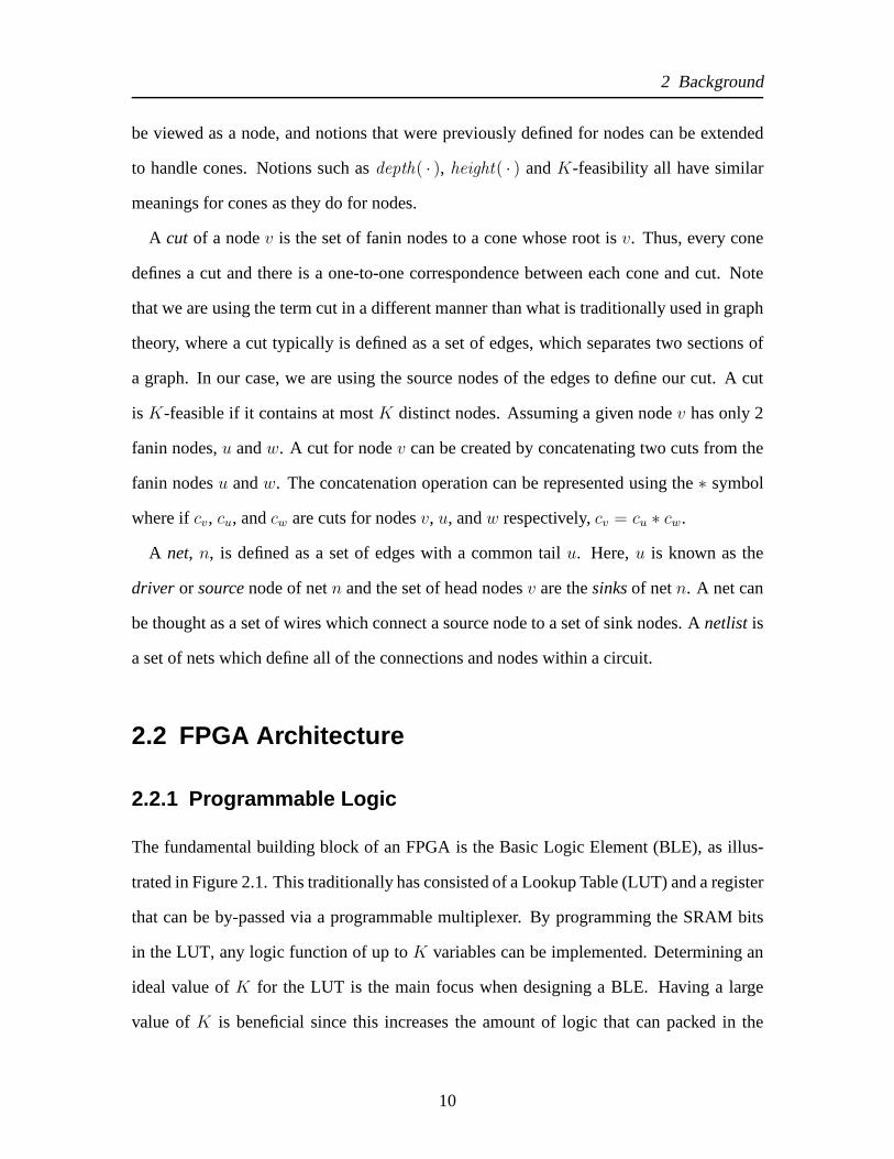
2.2.1 Programmable Logic
The fundamental building block of an FPGA is the Basic Logic Element (BLE), as illus-
trated in Figure 2.1. This traditionally has consisted of a Lookup Table (LUT) and a register
that can be by-passed via a programmable multiplexer. By programming the SRAM bits
in the LUT, any logic function of up toK variables can be implemented. Determining an
ideal value ofK for the LUT is the main focus when designing a BLE. Having a large
value ofK is beneficial since this increases the amount of logic that can packed in the
10

2 Background
. /01234567 /01
899:;;;<=>?@AB267. 23456 0CD
9EC3FGHI276HGHJK56456
Figure 2.1: A Basic Logic Element (BLE) consisting of a Lookup Table (LUT) and a con-figurable register.
BLE and reduces the number of BLEs along the critical path of the circuit. However, each
additional input to the LUT doubles its size thus finding a good balance between delay and
area is necessary. Previous work has shown that BLEs containing 4-input LUTs result in
the best area-delay balance [AR00]; though more recently, LUTs with 5 or 6 inputs have
been favoured to improve circuit delay [Mor06b, LAB+05] at the cost of some area.
BLEs are connected together via wire segments and programmable switches. How-
ever, there is a significant delay penalty associated with each connection switch a sig-
nal has to pass through. To mitigate this problem, FPGA architectures have adopted
a hierarchical structure, where BLEs are clustered together into larger blocks known as
Logic-Array Blocks (LABs) (the term Clustered Logic Block (CLB) is also commonly
used). The connection fabric within a LAB is often an order ofmagnitude faster than
the interconnect between LABs [RBM99]. Thus, by packing critical portions of a cir-
cuit into a small number of LABs, circuit delay improves dramatically. An example
of the hierarchical LAB structure is illustrated in Figure 2.2 where each LAB contains
n BLEs andI inputs. Previous work has shown that the number of required cluster
11

2 Background
LMNLMN
OPQRRSTUVWXP NLYZZZ[\ NLY]
^_^^^^_^^NLYNLY
`aMbcVX]LMN
d LMN VRefX]
g NLYVRefX] NLY
_̂̂hiiijk`aMbcVX]g VRefX Llm
^nlRopSqV]XSpSWrfXefX
sptqpQuuQcTS`vVXwP NTtwxsptqpQuuQcTSyRXSpRQTatfXVRq
LMNLMNOtRRSwXVtRNTtwx
Figure 2.2: The hierarchical structure of an FPGA.
inputs I can be significantly lower than the maximum value ofK × n for full logic
utilization within a LAB [BR97a, RBM99, AR00]. In particular, for BLEs containing
4-input LUTs, previous studies has shown that a good number of LAB inputs is I =
2n + 2 [BR97a, RBM99, AR00].
As Figure 2.2 shows, LABs are connected together with discrete routing segments where
each segment can host at most one inter-LAB signal. Connections between segments are
made using programmable multiplexers to determine which segments attach to a given
LAB. The number of segments found in a single channel is knownas thechannel-widthand
the channel-width together with the programmable switch blocks form the FPGA routing
fabric. Previous work has explored both the routing segmentstructure [BR99, LBJ+03]
and connections blocks [CFK96, Wil97] which yield good delay at a reasonable cost.
2.2.2 Commercial Architectures
In order to improve the versatility and performance of FPGAs, commercial FPGA archi-
tectures often add specialized blocks onto the FPGA which works in conjunction with the
12

2 Background
Logic Array Blocks (LABs)
M512 RAMBlocks
Phase-Locked Loops (PLLs)
DSP Blocks
M4K RAM Blocks
MegaRAM™Blocks
I/O Elements (IOEs)
Figure 2.3: Altera’s Stratix commercial FPGA [LBJ+03].
programmable logic. For example, Figure 2.3 has a high-level overview of Altera’s Stratix
FPGA [LBJ+03]. This consists of BLEs and programmable interconnect, along with mem-
ory and dedicated “hard” blocks. These hard blocks are high-performance structures which
can perform various arithmetic operations. An example of a typical hard block is shown
in Figure 2.4 which implements a multiply-accumulate operation. Since these structures
lack any programmable logic, they are much faster and smaller than a fully programmable
alternative. This both reduces the costs and enhances the performance of the FPGA. This
has led to more studies to both quantify the benefits of using hard blocks on FPGAs and
explore new structures that may be beneficial [JR05, LKJ+09].
2.3 FPGA CAD
The FPGA CAD flow has a major impact on performance of applications running on
FPGAs and each step is coupled very tightly to the underlyingFPGA architecture. These
13

2 Background
1.3.2 Multiply-Accumulator Mode
A
Scanout B
Scanout A
A
B Accumulator
Sign A
Sign B
Zero Acc
Sign A
Sign B
Data
Out
Acc
Overflow
Add / Sub 0
Figure 2.4: A multiply-accumulate “hard” block on the commercial Stratix FPGA [Alt05b].
steps are highlighted in Figure 2.5 and determine how efficiently a design gets maps onto
the programmable fabric of the FPGA.
2.3.1 Logic Synthesis and Technology Mapping
Logic synthesis is the first step in the CAD flow after a high-level description is converted
to atechnology independentnetlist. We define a technology independent netlist as a circuit
representation where each node represents a Boolean function that is not tied to any spe-
cific technological implementation. The goal of logic synthesis is to create an optimized
netlist consisting of basic gates, such as 2-inputANDandORgates [ESV92, MCB06a]. An
example of this is shown in Figure 2.6. In Figure 2.6(a), an unoptimized netlist is passed
to logic synthesis resulting in a less costly implementation as shown in Figure 2.6(b). Sev-
eral common techniques are used during logic synthesis to improve the area and delay of
14

2 Backgroundz{|}{~��������� ����������{����� z��{�����~��������� �|� {����� �}���{��{�}�
����{�}���|������{����{�����{}|��{��
������z��
��� ¡¢ £¤¤ ¥¦ §¨¢©ª«¦ ¬
������|����}�®��z��{���������¯��������}��{�} �����{�°�±|{����|}|°�{�}�
��²��}���|�����
���}�°��{|���|������{�
���|��|����� �|��³�}�¯��|{������
��z��zFigure 2.5: A generic CAD flow for FPGAs.
15

2 Background
a circuit including two-level minimization [BHMSV84], algebraic division [BM82], func-
tional decomposition [Ash59, RK62, JJHW97, YSC99, YCS00],rewiring [SB98, CLL02,
LJHM07], and rewriting [LSB05b, MCB06a].
x´xµ
F G
x¶ x·x¸ x¹
(a)
F G
xºx» x¼ x½x¾
(b)
F G
x¿xÀ xÁ xÂxÃ
(c)
F G
ÄÅÆÇÈ ÄÅÆÇÈxÉxÊ xË xÌxÍ
(d)
Figure 2.6: An illustration of the logic synthesis process and technology mapping. (a) Anunoptimized netlist. (b) An optimized netlist. (c) Identification of nodes to packinto a LUT for technology mapping. (d) Technology mapped circuit to 4-inputLUTs.
Once optimized, the netlist is then passed to the technologymapper which maps the
basic gates into technology specific nodes, such as 4-input LUTs [MBV06] as illustrated in
Figure 2.6(d). When mapping to LUTs, the goal is to pack as much logic as possible into
each LUT. This is beneficial since it minimizes the number of LUTs required to implement
the circuit. Other metrics such as delay and power should also be taken into consideration
during technology mapping. For example, in [AN06] the authors prove that static power
consumption of storing logic “1” versus a logic “0” is asymmetric and this can be leveraged
during technology mapping to reduce the FPGA power use.
16

2 Background
2.3.2 Clustering, Placement, and Routing
Clustering involves packing each BLE produced after technology mapping into a set of
LABs. One of the first works to effectively accomplish this was the VPACK tool [BR97a].
In VPACK, a greedy approach is used where BLEs are clustered one at a time. This starts
off with a seed BLE as the initial cluster. Next, additional BLEs are added to it based on an
attraction function. In VPACK, BLEs with more common connections to the current seed
cluster are chosen over other BLEs. This continues until thecurrent cluster utilizes all of
the logic or inputs into the LAB. Next, a new cluster is started until all BLEs are clustered
into LABs. VPACK was later improved in T-VPACK to include timing information into
its attraction function [MBR99]. More recently, routing considerations were taken into
account [SMS02, BMYS04] which was shown to reduce the overall area and power use of
the resulting netlist. A useful side-effect of clustering is that it can significantly reduce the
number of placeable objects in the circuits. This in turn reduces the solution space of the
placement problem.
During placement, each LAB is assigned to a single location on the FPGA chip such
that the overall interconnect use and circuit timing is minimized. Although several place-
ment techniques have been explored in the past, simulated annealing, as exemplified by
VPR [BR97b], has become the de facto standard for FPGA placement. During simulated
annealing based placement, individual LABs are randomly swapped between locations.
The swaps are accepted if circuit metrics such as wirelengthor timing is improved1. Dur-
ing placement, wirelength is estimated as the summation of thehalf-perimeterlength of all
nets within the design. An example of the half-perimeter of anet is shown in in Figure 2.7.
For timing-driven placement, the delay between two LABs is estimated using a lookup
method where the delay between two locations is precalculated empirically and cached in a
1To avoid getting "trapped" in local minima, simulated annealing will often accept moves which hurt timingor wirelength, so long as this improves the timing and wirelength in succeeding swaps [BR97b].
17
2 Background
lookup table [MBR00]. Along with several heuristics such ashill-climbing, simulated an-
nealing based placement has proved to be an extremely effective means to solve the FPGA
placement problem. One drawback of simulated annealing is its computational complex-
ity. As a result, placement has traditionally consumed the majority of the runtime in the
FPGA CAD flow; however recent advancement in parallelization [LBP08] and partition-
ing [SR99] has significantly reduced the runtime of FPGA placement to manageable levels.
ÎÏÐÑÒÓÔÕÖ×ØÙÖÚÖ× Û ÎÜÏ
Figure 2.7: The half-perimeter wirelength of a net is definedas half of the rectangle perime-ter which encompasses all terminals of the net. This rectangle is termed as abounding box.
Once placement completes, routing begins. During routing,LABs are connected to-
gether via programmable connections and wire segments. Dueto the discrete nature of
the FPGA routing problem, FPGA routing is significantly moredifficult than the general
routing problem found in ASICs. One of the more general approaches to FPGA routing is
PathFinder [ME95]. PathFinder connects LABs together suchthat the wire delay is min-
imized between connections. During this initial step, wiresegments can be used more
than once to create connections between LABs. Once all required connections are made,
a second routing iteration starts which “rips out” overusedwire segments. The cost of
the overused segments is incremented to deter the router from overusing them again. This
process continues until no more wire segments are overused.
18

2 Background
2.3.3 Physically-Driven Synthesis
Physically-driven synthesis, or physical synthesis for short, has become an important step
in achieving timing closure after placement. During physical synthesis, logic transforma-
tions are applied in conjunction with timing information derived from the placement. An
example of this is shown in Figure 2.8. Here we show a basic retiming operation where
registers are “pushed” across the circuit to shorten the register-to-register delay of the cir-
cuit [LS91, SMB05b]. Retiming is a popular means to optimizecircuit delay since it does
not change the cycle behaviour of the circuit, thus externalinterfaces to the circuit do not
need to be changed. In Figure 2.8(a), we show an unclustered netlist at the top and the
clustered and placed netlist below it. In this figure, each LAB is represented by a large
block and can pack at most four BLEs. Assuming that the delay between two BLEs is
proportional to their distance, shortening the length of the critical path will improve the
circuit delay. This is highlighted in Figure 2.8(b) where register d is pushed ahead of logic
element c. Although this shortens the path between logic element c and register d, the cur-
rent placement is now illegal since the pushed register is assigned to a full LAB. In order
to create a legal placement, the cells surrounding registerd must be displaced such that the
resulting placement is legal as shown in Figure 2.8(c) and Figure 2.8(d). This iterative pro-
cess between logic transformations and incremental placement continues until the circuit
delay converges to a desired value.
2.3.4 Engineering Change Orders (ECOs)
Engineering Change Orders (ECOs) cover a wide range of work which is either used to in-
crementally improve the delay of a design [CS00] or help modify the behaviour of a design
such that circuit delay is maintained [MCB89, CMB08, YSVB07, HCC99, Men05, Xil08].
The work presented in this dissertations falls in the lattercategory where we focus on late-
19

2 Background
ÝÞßÝÞß ÝÞßà áâ ã äà âã
ä á(a)
åæçåæç åæçè éê ë ìè êëé
ì(b)íîïíîï íîïð ñò ó ô
ð òóô
ñ(c)
õö÷õö÷ õö÷ø ùú û üø ú û
üù
(d)
Figure 2.8: Illustration of physically-driven synthesis applying retiming. (a) Current place-ment with long distance between register d and logic elementc. (b) Post-placement layout-driven optimization using retiming. (c)Incremental place-ment process for legalization. (d) Final legal placement ofoptimized netlist.
20

2 Background
stage ECOs that are applied directly to a place-and-routed netlist. Late-stage functional
changes often occur due to last minute feature changes or dueto bugs which have been
missed in previous verification phases. The most recent steps toward the automation of the
ECO experience include [CMB08] and [YSVB07]. Here, using formal methods and ran-
dom simulation, the authors in [CMB08, YSVB07] show how netlist modifications can be
automated. To apply modifications, the authors use random simulation vectors to stimulate
the circuit. Using the resulting vectors at each circuit node, they are able to find suggested
alterations to their design to match a specified behaviour. Following their modifications,
they require a formal verification step to ensure that their modification is correct. The re-
sults of their work is promising where they can automatically apply ECOs in more than
70% of the cases they present.
The technique in [YSVB07, CMB08] requires an explicit representation of any modifi-
cation, which does not scale to large changes. This is not a problem in ASICs since ECOs
requiring major changes are not desired since they are difficult to implement; however in
FPGAs, where we can reprogram individual logic cells, largechanges can be implemented
while maintaining circuit delay. Our approach improves on this where we can handle much
larger changes by using a SAT-based approach shown in Chapter 5.
2.3.5 Timing Analysis
Timing analysis occurs at every level of the FPGA CAD flow and is a main driver for circuit
optimizations aimed at improving the delay of the design. During timing analysis, every
node and edge within the circuit graph is assigned a delay value and critical portions of the
circuit are found. An example of this is shown in Figure 2.9 where each node and edge is
annotated with a delay value and the longest path delay of thecircuit,Delaymax, is shown.
This path is known as thecritical path of the circuit and determines the minimum clock
period (or maximum clock frequency) of the design.
21

2 Background
ýþÿ�þÿ �þÿ�þÿ ýþÿ�þÿ
����þÿ�þÿ ���
� � � ���þÿ �������������� � � !"#$%&''()&* � +!"',-.(',/ � 0!"
1*&23 � +45!"2'(6(2&*(67 � 8498:Figure 2.9: An illustration of a circuit graph with static timing values assigned to each node
and edge.
One simple method to timing analysis isstatic timing analysis. Static timing analysis
uses the static delay values of nodes and edges in the circuitgraph to calculate thecriticality
of each edge. Paths that contain many critical edges are optimized for delay.
The criticality of an edge inversely relates to the amount of flexibility an edge has to
increase its delay where critical edges have very little flexibility to increase its delay without
harming the clock frequency of the circuit. This flexibilityis based on the notion ofarrival
timeandrequired time. The arrival time is defined by Equation 2.1. In Equation 2.1,the
arrival time of a nodev is defined as the maximal value of the arrival time of a fanin to
nodev plus the delay of the fanin node and its edge connection,delay(u) + delay(〈u, v〉).
Basically, the arrival time of nodev is the longest path delay from a primary input to the
22

2 Background
nodev.
arrival(v) =
MAXu∈fanin(v){delay(〈u, v〉) + arrival(u)} +delay(v),
if v 6= {PI, register}
0, otherwise
(2.1)
The required times of each node is defined by a similar relationship as defined in Equa-
tion 2.2 which is the longest path delay between nodev and a primary output.
required(u) =
MINv∈fanout (u){required(v)− delay(〈u, v〉)} −delay(u),
if u 6= {PO, register}
Delaymax, otherwise
(2.2)
Using the arrival time and required time, we can defineslackas shown in Equation 2.3.
To find the criticality of each edge, we first normalize the slack to the largest arrival time
value, as shown in Equation 2.4. This is known as the slack ratio of the edge. Finally, using
the slack ratio, we can define the criticality of each edge as defined by Equation 2.5. Here,
the criticality ofv is defined as 1 minus the slack ratio ofv. The criticality of an edge takes
on the value between 0 and 1. Nodes which are attached to critical edges with a value equal
to or near 1 should be optimized for delay to help shorten the critical path.
slack(〈u, v〉) = required(v)− arrival(u)− delay(〈u, v〉) (2.3)
slackratio(〈u, v〉) =slack(〈u, v〉)
Delaymax
(2.4)
criticality(〈u, v〉) = 1− slackratio(〈u, v〉) (2.5)
The primary difficulty in performing static timing analysisis assigning accurate delay
23

2 Background
values to each node and edge. The most simplistic pre-placement delay model usesunit
delay. In the unit delay model, the delay of each edge is assigned a value of 0 and nodes
have a unit delay value. Various other more sophisticated delay estimation methods have
been applied for logic synthesis such asnetrange[LMS04]. The netrange of a net is de-
fined as the difference between the minimum and maximum logicdepth of any given node
connected to a net where the delay of a net is proportional to its netrange. Unfortunately,
effective pre-placement delay models are still lacking andrequire further work [MCSB06].
Post-placement delay estimation is much easier since the relative position of logic blocks,
and hence the approximate length of interconnect segments is well defined. Thus, after
placement and routing has completed estimations of delay values in the circuit is very ac-
curate. Leveraging this information can be extremely powerful when trying to improve cir-
cuit clock frequency. This occurs during the physically-driven synthesis and Engineering
Change Orders step where placement information is used to help guide logic transforma-
tions to incrementally increase the circuit clock frequency or modify its behaviour.
2.4 Introduction to Binary Decision Diagrams
A Binary Decision Diagram (BDD) is a directed acyclic graph that represents a Boolean
function. A BDD can be understood in terms of Shannon’s expansion [Sha38], as shown in
definition 2.4.1.
Definition 2.4.1 Shannon’s expansion:
F (x0, x1, ..., xn) = x0 ·F (0, x1, ..., xn) + x0 ·F (1, x1, ..., xn) (2.6)
In definition 2.4.1,F (0, x1, ..., xn) andF (1, x1, ..., xn) are the negative and positive cofac-
tors of functionF with respect to variablex0 respectively. The negative cofactor can be
represented asF |x0and the positive cofactor can be represented asF |x0
. Definition 2.4.1
24

2 Background
states that any Boolean expression can be represented as a summation of a variable and
its complement conjoined with its respective cofactor. Shannon’s expansion can be repre-
sented graphically as shown in Figure 2.10. Here, the dottedline represents the negative
assignment tox0, and the solid line represents a positive assignment.;<=; >? ; >?@ @Figure 2.10: Graphical representation of Shannon’s expansion.
A BDD extends the graph shown in Figure 2.10 to all variables in functionF . This is
illustrated in Figure 2.11 where we show the truth table, cube representation, and BDD
representation for the Boolean expressionf = x1x3x4 + x1x2x3 + x1x2x4. In the BDD
shown in Figure 2.11, each path from the root nodeF to a terminal node 0 or 1 represents a
minterm in functionF . The terminal value of that path represents the value ofF assuming
the minterm along that path is set to true.
The fully expanded BDD shown in Figure 2.11 is not very usefulsince it grows expo-
nentially with respect to the number of variables in the function. A more useful form is the
Reduced Ordered Binary Decision Diagram (ROBDD). A ROBDD significantly reduces
the size of a BDD by leveraging two reduction rules. The first one is illustrated in Fig-
ure 2.12. This removes nodes whose positive and negative edge point to the same node.
In Figure 2.12(a), we identify a node whose positive and negative edge point to the same
value 0. This is applied to all nodes resulting in the graph inFigure 2.12(d). Following
this, we remove redundant terminal nodes as illustrated in Figure 2.13(a). When applied to
all terminal nodes, the resulting graph is shown in Figure 2.13(b).
25

2 Background
x1x2x3x4 F0000 00001 00010 10011 00100 00101 00110 10111 01000 01001 01010 01011 01100 11101 11110 01111 1
(a) Truth-table
x1x2x3x4 F0-10 1110- 111-1 1(b) Cubes
AB ACADE E
FAGAG AC ABAB ABH E E E H E E E E E H H E HAG AGAG AGAG AG
(c) BDD
Figure 2.11: Truth-table, cube, and Binary Decision Diagram (BDD) representation offunctionf = x1x3x4 + x1x2x3 + x1x2x4.
26

2 Background
IJ IKILM M
NIOIO IK IJIJ IJP M M M P M M M M M P P M PIO IOIO IOIO IO
(a)
QR QSQTU
VQWQW QS QRQR QRX U U U X U U U U U X X U XQW QWQW QWQW QW
(b)
YZ Y[Y\]
^Y_Y[ YZYZ YZ` ] ] ] ` ] ] ] ] ] ` ` ] `Y_ Y_Y_ Y_Y_ Y_
(c)
ab acade
fac ababg e e g e e g e gah ah ah(d)
Figure 2.12: An illustration of reduction rule 1: removing redundant assignments.
27

2 Background
ij ikilm
nik ijij
m o m m o m oip ip ip(a)
qr qsqtuqs qrqrv w
qx qx qx(b)
Figure 2.13: An illustration applying reduction rule 1 to the entire graph: removing allredundant assignments.
28

2 Background
The second reduction rule is shown in Figure 2.14. Here, nodes that have the same
variable label and whose positive and negative edge point tothe same nodes can be replaced
with a single node. The parent edge of all nodes that are removed are then reattached to
the remaining node. This process is shown in figures 2.14(a) and 2.14(b). After applying
both of the reduction rules, the resulting ROBDD is shown in Figure 2.14(c). Generally
in literature, BDD is used synonymously with ROBDD and we will do the same in this
dissertation.
yz y{y|}y{ yzyz~ �
y� y� y�(a)
������� ����� �
�� ��(b)
���������
� ��� ��
(c)
Figure 2.14: An illustration of reduction rule 2: removing duplicate nodes.
29

2 Background
An interesting characteristic of BDDs is that every subgraph rooted at a single node and
terminated by the 0 and 1 terminal nodes represents a Booleanexpression. For example,
Figure 2.15(a) identifies the two expressions rooted at eachx3 node. This fact makes
BDD construction extremely efficient through dynamic programming. Here, subgraphs
can be reused to represent larger BDDs; this saves a significant amount of time and storage
space when manipulating BDDs [Som98]. We leverage this factto improve the algorithms
discussed in Chapter 3.
One additional reduction rule leverages the inverted representation of Boolean expres-
sions. Since each subgraph represents a Boolean expression, there may exists subgraphs
where are complements of each other. This is shown in Figure 2.15(a). We can reuse the
complemented form of a subgraph if we introduce inverted edges into the BDD. If a sub-
graph in the BDD is pointed to by an inverted edge, this implies that the terminal nodes are
inverted. This is shown in Figure 2.15(b) by the finely dottedline.
���������
� ��� �� �� � ������
(a)
���� �¡
¢ £�¤(b)
Figure 2.15: An illustration of using inverted edges.
BDDs have a canonical property where for a given variable ordering in the graph, and
assuming all of the previous reduction rules have been applied, there exists exactly one
30

2 Background
representation for a given Boolean function. For differentvariable order, the canonical
property does not hold. Furthermore, the number of nodes in the BDD varies dramatically
with variable order. For example, for the previous functionf = x1x3x4 +x1x2x3 +x1x2x4,
alternate variable orderings can lead to very different graphs as shown in Figure 2.16. Sev-
eral heuristics have been used to find a “good” ordering such that the size of the BDD is
minimized [Rud93].
¥¦¥§̈¥©
ª «¥¬(a)
®°̄±
² ³´® ± ±
(b)
Figure 2.16: An illustration of two resulting BDDs if alternate variable orders are used.
2.4.1 Zero-Suppressed Binary Decision Diagrams
The BDD data structure has been used in a wide range of applications for logic synthesis.
However, for some domains, BDDs are not well suited. As a result, there have been several
variants to the BDD data structure which have proved to be very useful for various applica-
tions [BFG+93]. One variation is the Zero-Suppressed Binary Decision Diagram (ZDD).
ZDDs differ from BDDs is one of its reduction rules. In BDDs, if the positive and negative
edge of a nodev point to the same nodeu, v is removed. In contrast, ZDDs will remove
a node if its positive edge points to the 0 terminal node. Thisvariation has major implica-
31
2 Background
tions on representing Boolean expressions. For example, Figure 2.17 illustrates a Boolean
expression represented as a BDD and as a ZDD.
µ¶µ·¸µ¹º »µ¼
(a)
½¾½¿À ½Á ýÄ
½¾½Á½Ä(b)
Figure 2.17: BDD and ZDD representation off = x1x2 + x3x4 [Mis01].
Figure 2.17 highlights that ZDDs are not good at representing generic Boolean functions.
However, when representing sets, ZDDs are extremely efficient. For example, consider
the set{x1x2, x1x3, x3}. When represented as its characteristic function [CM77], this is
represented asf = x1x2x3 + x1x2x3 + x1x2x3 whose BDD and ZDD representation is
shown in Figure 2.18. Clearly, the ZDD representation is much more efficient and as a
result, ZDDs have been widely used to quickly manipulate sets within CAD [Min93].
2.5 Introduction to Boolean Satisfiability
The Boolean Satisfiability (SAT) problem was introduced in 1971 as the first problem clas-
sified as NP-Complete [Coo71]. Given that P class problems have a polynomial run time,
it is generally thought that NP-Complete class problems areharder than P class problems.
This statement, although not formally proven, is often described byNP-C 6= P [CLRS01,
ch.34]. As a result, efficient heuristics must be applied to reduce the problem space and
time requirements for solving NP-Complete problems. Research in the area of SAT is an
32

2 Background
ÅÆÅÇÈÉ ÊÅËÅÆ ÅË
(a)
ÌÍÌÎÏÐ ÑÌÒ
(b)
Figure 2.18: BDD and ZDD representation of the characteristic function of{x1x2, x1x3, x3} [Mis01].
example of this where heuristics have demonstrated runtimeimprovements on a range of
NP-complete problems in the order of1000× in comparison to brute force methods.
Given a Boolean formulaF (x1, x2, ..., xn), SAT asks if there is an assignment to the
variables,x1, x2, ..., xn, such thatF evaluates to 1. If such an assignment exists,F is said
to besatisfiable, otherwise, it isunsatisfiable. A SAT solver serves to answer the SAT
problem.
(A + B + C)︸ ︷︷ ︸
· (A + B + C︸︷︷︸
)
clause literal
Figure 2.19: A Boolean formula in Conjunctive Normal Form.
For practical purposes, modern day SAT solvers work on Boolean formulae in Conjunc-
tive Normal Form (CNF). Boolean formulae in CNF consist of a conjunction of clauses.
A clause is a disjunction (logicalOR) of literals and a literal is any Boolean variable,
x ∈ {0, 1}, or its complement. An example Boolean expression in CNF is shown in Fig-
ure 2.19. Any Boolean formula can be converted to CNF using basic Boolean algebraic
33

2 Background
Logic Operation Symbolic Representation CNFDe Morgan’s Law (A + B) (A ·B)
(A ·B) (A + B)
Implication (A −→ B) (A + B)
Equivalence (A←→ B) (A + B) · (A + B)
Table 2.1: Conversion rules for CNF Construction.
techniques such as those shown in Table 2.1.
In CNF, the problem of SAT can be rephrased to the following: Given a Boolean formula,
F (x1, x2, ..., xn), in Conjunctive Normal Form (CNF), seek an assignment to thevariables,
x1, x2, .., xn, such that each clause has at least one literal evaluating to1. Interestingly,
when dealing with CNF Boolean formulae whose clauses all have fewer than three literals,
SAT is a polynomial problem [CLRS01, ch.34]. Once there exists at least one clause with
three or more literal terms, the problem becomes NP-Complete [CLRS01, ch.34].
2.6 Solving the Boolean Satisfiability Problem
One of the earliest works on SAT was done in 1960 by Davis and Putnam in [DP60]. This
was refined a few years later by Davis, Logemann, and Lovelandin [DLL62] to create the
DPLL algorithm. The DPLL algorithm was originally applied to theorem proverswhich
attempt to verify a set of propositional statements. The DPLL algorithm is based upon the
splitting rulewhich can be understood in terms of Shannon’s expansion [Sha38], as shown
in Definitions 2.6.1 and 2.6.2.
Definition 2.6.1 Shannon’s expansion:
F (x0, x1, ..., xn) = x0 ·F (0, x1, ..., xn) + x0 ·F (1, x1, ..., xn) (2.7)
Definition 2.6.2 Splitting Rule:F (x0, x1, ..., xn) is satisfiable if and only if
F (0, x1, ..., xn) is satisfiable orF (1, x1, ..., xn) is satisfiable.
34

2 Background
sat_solve(F, V, A)begin
if (F (A) ≡ 1)return satisfiable
if (F (A) ≡ 0)return unsatisfiable
// select a variable and assign it to 0// to check if F(0,...) is satisfiableselect a variablep ∈ VassignV ← (V − p)assignp← 0assignA← (A
⋃p)
if (sat_solve(F, V, A) ≡ satisfiable)return satisfiable
// 0 assignment failed, assign it to 1// to check if F(1,...) is satisfiableassignA← (A− p)assignp← 1assignA← (A
⋃p)
if (sat_solve(F, V, A) ≡ satisfiable)return satisfiable
// Formula is not satisfiable under the current assignment.unassignpassignA← (A− p)assignV ← (V
⋃p)
return unsatisfiableend
Algorithm 2.1: A recursive algorithm to solve SAT.
The splitting rule naturally defines a simple recursive algorithm for SAT shown in Algo-
rithm 2.1. Algorithmsat_solve accepts three parameters: the functionF, a set of variables
V that defineF, and a set of assignmentsA to the variables inV. Firstsat_solve checks if
the current assignment leads to a satisfiable or unsatisfiable solution. IfF is in an indeter-
minate state with respect to the current set of assignments,sat_solve selects an unassigned
variable (referred to as afree variable) and assigns it the value 0.sat_solve then recur-
sively checks if the remainder of the formula is satisfiable;if so, it returns satisfiable. If
35

2 Background
not, it toggles the last variable assignment to 1 and repeatsthe recursive check. If both
assignments lead to an unsatisfiable solution,sat_solve returns unsatisfiable.
Algorithm 2.1 is horribly inefficient; however, it is the core of all modern day SAT
solvers, which have come a long way since the first DPLL algorithm. Some popular ones
include Chaff, Grasp, and SATO [MMZ+01, MSS99, Zha97]. The reason for their suc-
cess stems from heuristics which can drastically reduce thesearch space of the SAT solver.
These heuristics include, but are not limited to, Boolean Constant Propagation, conflict-
driven learning, and non-chronological backtracking. Forthe interested reader, the fol-
lowing sections explains these concepts in detail, but is not necessary to understand the
successive chapters in this dissertation.
2.6.1 Heuristics To Solve the Boolean Satisfiability Proble m
Boolean Constant Propagation
Boolean Constant Propagation (BCP) reduces the search space by ignoring decisions that
will create an obvious unsatisfiable state. BCP works by taking advantage ofunit clauses
to force variable assignments in animplicationprocess. A unit clause is a clause with only
one free literal where all other literals in the clause evaluate to 0. Thus to satisfy a unit
clause, the implication process forces the free literal to evaluate to 1. For example, given
the assignment shown in Figure 2.20,x4 must be assigned to 0 to satisfy the expression.
(x1 + x2) · (x2 + x3 + x4)︸ ︷︷ ︸
unit clause
Figure 2.20: An example of a unit clause, given thatx1x2x3 = 110 andx4 is free.
36
2 Background
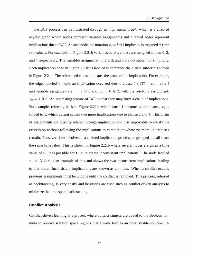
The BCP process can be illustrated through animplication graph, which is a directed
acyclic graph where nodes represent variable assignments and directed edges represent
implications due to BCP. At each node, the notationxi = b @ l impliesxi is assigned at time
l to valueb. For example, in Figure 2.21b variablesx1, x4, andx8 are assigned at time 0, 2,
and 4 respectively. The variables assigned at time 1, 3, and 5are not shown for simplicity.
Each implication edge in Figure 2.21b is labeled to reference the clause subscripts shown
in Figure 2.21a. The referenced clause indicates the cause of the implication. For example,
the edges labeled 1 imply an implication occurred due to clause 1 ((x1 + x4 + x2)1 )
and variable assignmentsx1 = 1 @ 0 andx4 = 0 @ 2, with the resulting assignment,
x2 = 1 @ 6. An interesting feature of BCP is that they may form a chain ofimplications.
For example, referring back to Figure 2.21b, when clause 1 becomes a unit clause,x2 is
forced to 1, which in turn causes two more implications due toclause 2 and 4. This chain
of assignments are directly related through implication and it is impossible to satisfy the
expression without following the implications to completion where no more unit clauses
remain. Thus, variables involved in a chained implication process are grouped and all share
the same time label. This is shown in Figure 2.21b where several nodes are given a time
value of 6. It is possible for BCP to create inconsistent implications. The node labeled
x7 = X @ 6 is an example of this and shows the two inconsistent implications leading
to that node. Inconsistent implications are known as conflicts. When a conflict occurs,
previous assignments must be undone until the conflict is removed. This process, referred
as backtracking, is very costly and heuristics are used suchas conflict-driven analysis to
minimize the time spent backtracking.
Conflict Analysis
Conflict-driven learning is a process whereconflict clausesare added to the Boolean for-
mula to remove solution space regions that always lead to an unsatisfiable solution. A
37

2 Background
F = ... · (x1 + x2)0 · (x1 + x4 + x2)1 · (x2 + x6)2 · (x4 + x2 + x1)3 ·
(x2 + x5 + x8)4 · (x4 + x6 + x7)5 · (x4 + x5 + x7)6 · ...(2.8)
(a) Boolean formula to illustrate BCP andconflicts.xÓ=1 @ 0
xÔ=0 @ 2
xÕ=1 @ 6
xÖ=1 @ 6
x×=1 @ 6
xØ=X @ 6
xÙ=1 @ 4
1
14
2
4
6
5
(b) Resulting implication graph from (a).
F = ... · (x1 + x4 + x8)(c) Conflict clause added due to conflict in (b).
(2.9)
Figure 2.21: A conflict-driven analysis implication graph.
detailed algorithm of this can be found in [MSS99] and is not discussed here, but referring
back to Figure 2.21, a quick explanation can be presented through an example. As stated
previously, nodex7 = X @ 6 is in conflict due to the conflicting implication edges 5 and 6,
thus backtracking must occur to undo this conflict. However,without learning it is possible
that this conflict arrangement may occur again; thus, it is beneficial to add information to
the Boolean formula to prevent this. Closer inspection of the implication graph in Fig-
ure 2.21 shows that the conflict originates at edges 1 and 4 dueto assignmentsx1 = 1,
x4 = 0, andx8 = 1. Further analysis of Equation 2.8 shows that assignmentx1 = 1,
38

2 Background
x4 = 0, andx8 = 1 will always cause a conflict. Thus, to prevent this in the future, a learnt
clause is added which is shown in Equation 2.9. The learnt clause is a redundant clause and
does not change the meaning of the original Boolean formulae, but it makes it impossible
for the assignmentx1 = 1, x4 = 0, andx8 = 1 to occur again.
Non-Chronological Backtracking
The process of reversing the most recent assignments due to aconflict is called chrono-
logical backtracking (i.e. in-order backtracking). However, often several assignments can
be reversed out of order if the source of the conflict can be identified. This is known
as non-chronological backtracking. Like conflict analysis, non-chronological backtrack-
ing uses conflict information to determine the original source of the conflict and reverse
all the decisions to that source. Continuing with the example in Figure 2.21, the original
source of the conflict was due to nodex8 = 1 @ 4. Thus, the backtracking process should
jump to decision level 4 to fix the conflict. This is depicted inthe decision treeshown
in Figure 2.22b which contrasts with chronological backtracking shown in Figure 2.22a.
A decision tree represents the variable assignment processwhere each branch represents
an assignment decision and each leaf represents a satisfiable or unsatisfiable solution. In
the case of unsatisfiable solutions, the decision tree backtracks up the tree to remove the
conflict.
2.6.2 Circuits and Boolean Satisfiability
The benefit of using SAT for problems in CAD is that circuit properties can be quickly
evaluated using any efficient SAT solver [McM03, SVV04, LSB05b, SMV+07, LJHM07].
However, before a circuit CAD problem can be formulated as a SAT problem, the circuit
must be converted to a Boolean formula in CNF form. This can beachieved using a tech-
nique first presented in [Lar92], which derives acharacteristic functionof a logic circuit.
39

2 Background
xÚ=1 @ 0
xÛ=1 @ 1
xÜ=0 @ 2
xÝ=1 @ 3
xÞ=0 @ 4
xÚß=0 @ 5
xà=0 @ 6 xà=1 @ 6
xÞ=1 @ 4
(a) Chronological backtracking.
xá=1 @ 0
xâ=1 @ 1
xã=0 @ 2
xä=1 @ 3
xå=0 @ 4
xáæ=0 @ 5
xç=0 @ 6 xç=1 @ 6
xå=1 @ 4
(b) Non-chronological backtracking.
Figure 2.22: Backtracking due to a conflict in Figure 2.21.
A B Z FAND
0 0 0 10 0 1 00 1 0 10 1 1 01 0 0 11 0 1 01 1 0 01 1 1 1
AZ
B
0
1
1
0
1
0
1
0
ABZ 00 01 11 10
0
1
FAND = (A + Z) · (B + Z) · (A + B + Z)
Figure 2.23: A characteristic equation derivation for 2-inputANDgate.
This CNF representation contain variables representing the primary input, primary output,
and intermediate circuit signals and evaluates to 1 if thesesignals are consistent. For ex-
40
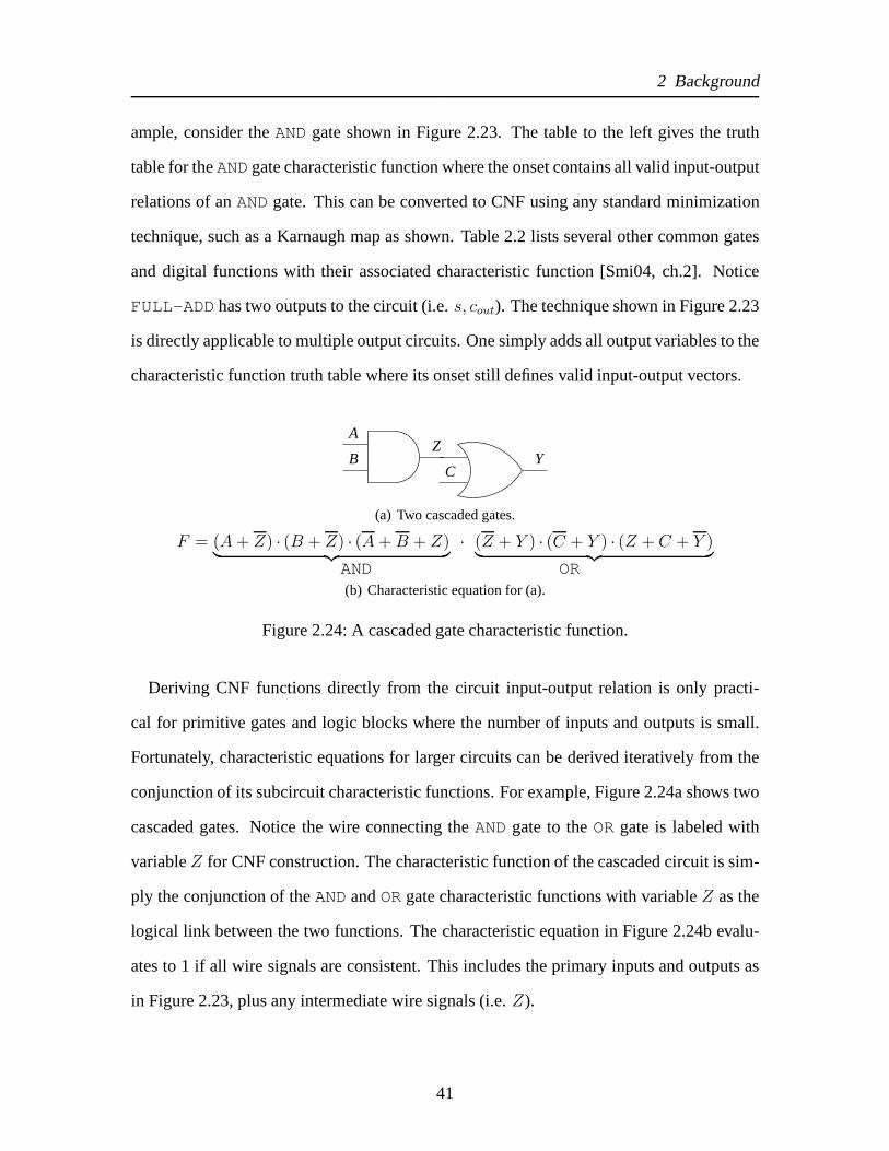
2 Background
ample, consider theANDgate shown in Figure 2.23. The table to the left gives the truth
table for theANDgate characteristic function where the onset contains all valid input-output
relations of anANDgate. This can be converted to CNF using any standard minimization
technique, such as a Karnaugh map as shown. Table 2.2 lists several other common gates
and digital functions with their associated characteristic function [Smi04, ch.2]. Notice
FULL-ADDhas two outputs to the circuit (i.e.s, cout). The technique shown in Figure 2.23
is directly applicable to multiple output circuits. One simply adds all output variables to the
characteristic function truth table where its onset still defines valid input-output vectors.
YC
BZ
A
(a) Two cascaded gates.
F = (A + Z) · (B + Z) · (A + B + Z)︸ ︷︷ ︸
· (Z + Y ) · (C + Y ) · (Z + C + Y )︸ ︷︷ ︸
AND OR(b) Characteristic equation for (a).
Figure 2.24: A cascaded gate characteristic function.
Deriving CNF functions directly from the circuit input-output relation is only practi-
cal for primitive gates and logic blocks where the number of inputs and outputs is small.
Fortunately, characteristic equations for larger circuits can be derived iteratively from the
conjunction of its subcircuit characteristic functions. For example, Figure 2.24a shows two
cascaded gates. Notice the wire connecting theANDgate to theORgate is labeled with
variableZ for CNF construction. The characteristic function of the cascaded circuit is sim-
ply the conjunction of theANDandORgate characteristic functions with variableZ as the
logical link between the two functions. The characteristicequation in Figure 2.24b evalu-
ates to 1 if all wire signals are consistent. This includes the primary inputs and outputs as
in Figure 2.23, plus any intermediate wire signals (i.e.Z).
41

2 Background
Gate Function CNF formula
AND y = x1 ·x2 · · ·xn
(n∏
i=1
(xi + y)
)
·
((n∑
i=1
xi
)
+ y
)
NAND y = x1 ·x2 · · ·xn
(n∏
i=1
(xi + y)
)
·
((n∑
i=1
xi
)
+ y
)
OR y = x1 + x2 + · · ·+ xn
(n∏
i=1
(xi + y)
)
·
((n∑
i=1
xi
)
+ y
)
NOR y = x1 + x2 + · · ·+ xn
(n∏
i=1
(xi + y)
)
·
((n∑
i=1
xi
)
+ y
)
XOR y = x1 ⊕ x2
(x1 + x2 + y) · (x1 + x2 + y) ·
(x1 + x2 + y) · (x1 + x2 + y)
NXOR y = x1 ⊕ x2
(x1 + x2 + y) · (x1 + x2 + y) ·
(x1 + x2 + y) · (x1 + x2 + y)
BUFFER y = x (x + y) · (x + y)
NOT y = x (x + y) · (x + y)
MUX 2:1 y = (s0 ↔ 1) ? x1 : x0
(s0 + x0 + y) · (s0 + x0 + y) ·
(s0 + x1 + y) · (s0 + x1 + y)
MUX 4:1
y = (s1 ↔ 1) ?
[(s0 ↔ 1) ? x3 : x2] :
[(s0 ↔ 1) ? x1 : x0]
(s0 + s1 + x0 + y) · (s0 + s1 + x0 + y) ·
(s0 + s1 + x1 + y) · (s0 + s1 + x1 + y) ·
(s0 + s1 + x2 + y) · (s0 + s1 + x2 + y) ·
(s0 + s1 + x3 + y) · (s0 + s1 + x3 + y)
FULL-ADDs = a⊕ b⊕ cin
cout = (a⊕ b) · cin + ab
(a + b + cout) · (a + b + cout) ·
(a + cin + cout) · (a + cin + cout) ·
(b + cin + cout) · (b + cin + cout) ·
(s + a + cout) · (s + a + cout) ·
(s + b + cout) · (s + b + cout) ·
(s + cin + cout) · (s + cin + cout) ·
(s + a + b + cin) · (s + a + b + cin)
Table 2.2: Characteristic functions for basic logic elements [Smi04, ch.2].42
2 Background
2.7 Relationship between Binary Decision Diagrams
and Boolean Satisfiability
In the previous two sections, we explored the properties of BDDs and SAT. We learnt that
the BDD explores properties of a circuit by storing Boolean expressions as a graph; whereas
SAT maps a circuit to a characteristic function and then applies a sequential algorithm to
traverse the function. BDDs have had a long history in CAD spanning several decades.
When applied to CAD, BDD graphs can be manipulated using fastBDD operators and
through dynamic programming which can be exploited due to the DAG structure of the
BDD. This had made BDDs extremely attractive in the past. However, the problem with
BDDs is that they suffer from memory explosion. Here, a givenBDD may require an
exponentially large number of nodes to represent a given Boolean expression. This has
created a wall in extending the application of BDDs to new areas.
Only in the last decade has SAT become popular in CAD. This hasprimarily been due to
the recent innovations started by the zChaff project [MMZ+01] which incorporated several
heuristics to significantly speed up the SAT process. UnlikeBDDs, SAT does not suffer
from memory explosion to the extent that BDDs do, since thereis a one-to-one correspon-
dence between the characteristic function of a circuit and the circuit size. The characteristic
function allows SAT to traverse the CNF to explore various properties of the circuit. The
drawback with this is that runtime becomes the limiting factor for SAT, where for some
SAT instances, the runtime of solving a problem is intractable.
Thus, there exists a complementary relationship between BDDs and SAT where BDDs
explore problems in space and SAT explore properties in time. For smaller problem in-
stances, BDDs are in general a faster means to solve problemsthan SAT. However, more
recently, more problems are finding a SAT-based solution which have been proved to be
much more scalable. This does not imply that SAT-based solutions will subsume all BDD-
43

2 Background
based solutions in the future, but simply illustrates that SAT and BDDs will continue to
play an important and synergistic role within CAD.
2.8 Summary
An overview of the primary architectural features of an FPGAwas given. First the BLE
was introduced as the basic building block of an FPGA. Following this, the LAB was
introduced and the benefits of using an hierarchical architecture was discussed followed by
a brief overview of the programmable routing fabric.
Following an architectural overview, the FPGA CAD flow was described. This disserta-
tion focuses primarily on improving the CAD flow where our goal is to improve the user
experience and scalability of existing CAD algorithms; specifically in logic synthesis and
ECOs.
The chapter then concludes with a brief overview of the Binary Decision Diagram data
structure and Boolean Satisfiability problem. These two problem domains share a com-
plementary relationship: BDDs solve Boolean expressions in space through a graph data
structure whereas SATs solves Boolean expressions in time through several algorithmic
approaches. In general, SAT based approaches to solving CADproblems has emerged as
more scalable than BDD based approaches and its applicationin CAD has grown in recent
years to many problem domains.
44

3 Improving BDD-based Logic Synthesis
through Elimination and
Cut-Compression
In a progression towards a more scalable and manageable FPGACAD flow, we investigate
methods to improve logic synthesis. We focus on logic synthesis since it has the most
flexibility to modify the circuit structure and has a large overall impact on the final circuit
performance. Furthermore, logic synthesis occupies a significant portion of runtime. In this
chapter we present means to help reduce the runtime of logic synthesis without impacting
the Quality of Result (QoR) of the optimized netlist.
The rest of the chapter will be organized as follows. Section3.1 will provide a brief
overview of the logic synthesis flow. Section 3.2 will describe some problems associated
with the existing logic synthesis flow. Specifically, we showhow existing techniques do
not scale to large circuit designs. Section 3.3 will outlineour solution to the problems we
discuss in the proceeding sections. Here, we propose a scalable approach to a key step
during logic synthesis: elimination. In doing so, we introduce a novel BDD-based cut
generation method that is an order of magnitude faster than previous approaches. Also, we
describe a new structural metric referred to asedge flowwhich helps reduce circuit area.
Section 3.4 will give an overview of our results and the chapter will conclude in Section 3.5.
45

3 Improving BDD-based Logic Synthesis through Eliminationand Cut-Compression
3.1 Introduction to Logic Synthesis
In the FPGA CAD flow, logic synthesis occurs after a high-level description is broken
down into basic logic gates. During logic synthesis, the goal is to optimize the circuit
netlist such that the resulting netlist has a more cost-effective implementation or has better
performance. Although there have been several generic flowsto the logic synthesis prob-
lem [ESV92, CJJ+03, MCB06a], in this work we focus on BDD-based synthesis flows.
BDD-based logic synthesis has gained popularity due to its compact representation of logic
function and scalable transformation techniques [YCS00, WZ05]. During BDD-based syn-
thesis, several generic steps are generally taken as shown in Figure 3.1. The first step taken
is elimination. The purpose of elimination is to remove redundancies within the circuit
netlist and form resynthesis regions in which succeeding optimizations can be applied. Af-
ter elimination,decompositionandshared-extractioncan occur. During this step, the resyn-
thesis regions formed during the elimination step are resynthesized such that the resulting
circuit is optimized. This process continues until the circuit meets some cost metrics or
no further improvement is achieved, after which the netlistis then passed onto technology
mapping.
3.2 Motivation
There has been a large body of work which has improved the decomposition and shared-
extraction step in logic synthesis; both to improve its QoR [BM82, Ash59, RK62, JJHW97]
and to improve its scalability [YSC99, YCS00, WZ05, MCB06a]. However, little focus
has been given to the elimination step. As a result, elimination has emerged as the primary
bottleneck for scalability in BDD-based synthesis engineswhere it has been reported to
take up to 70% of the runtime [WZ05]. During elimination, regions are grown from a
seed node where its fanins are successively collapsed into the node in a greedy fashion.
46
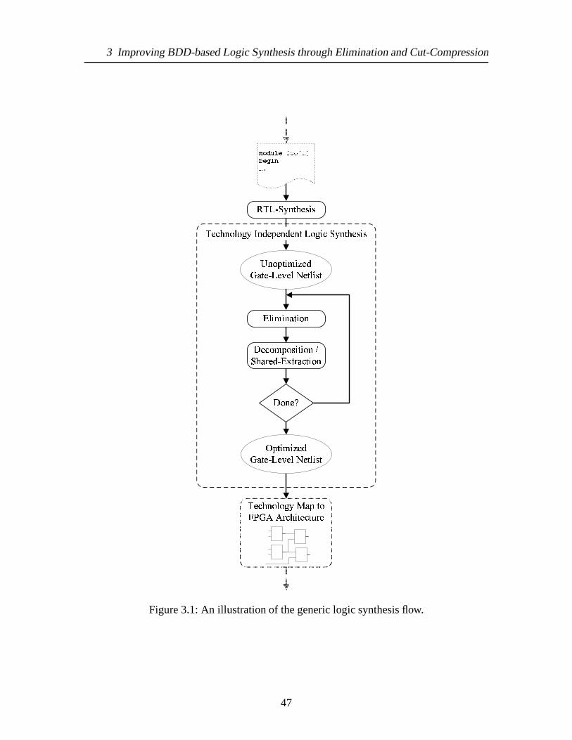
3 Improving BDD-based Logic Synthesis through Eliminationand Cut-Compression
èéêëìíîíïð ñòó ôíõö÷ø øùêëúôéêôûùé
üýþÿ�� ��� ���������è ��ðìôëé�ú�èéêëìíîíïð �ì�éóéì�éìô íïúê �ðìôëé�ú��ìíóôú�ú�é�÷òôé� é�éî �éôîú�ô�îú�úìòôúíì�éêí�óí�úôúíì ��ëòùé����ôùòêôúíì�óôú�ú�é�÷òôé� é�éî �éôîú�ô
�íìé�
Figure 3.1: An illustration of the generic logic synthesis flow.
47

3 Improving BDD-based Logic Synthesis through Eliminationand Cut-Compression
If the cost of the logic is reduced after the collapse, the collapse is committed into the
netlist, otherwise the collapse is undone. We measure simplification in terms of BDD
nodes, where we aim to reduce the number of BDD nodes after a collapse. This process is
illustrated in Figure 3.2. Figure 3.2(a) shows an unoptimized gate-level netlist. This netlist
is transformed to its BDD-based netlist representation in Figure 3.2(b) where each basic
gate in the original netlist is mapped to a logic node, whose logic function is represented
by a BDD. Next, a collapse operation is illustrated in Figure3.2(c) and 3.2(d) starting
from a randomly chosen seed node. Notice that after the collapse operation completes, the
number of resulting BDD nodes is reduced from 12 to 9 (terminal ’1’ and ’0’ nodes are not
included in the count). In situations where there is an increase in BDD nodes, the collapse
would be undone. After several collapse operations are done, the resulting netlist is shown
in Figure 3.2(e) resulting in 4 BDD nodes contained in a single elimination region (for
larger circuits, several elimination regions would result). Following this, a decomposition is
applied to decompose the netlist back into basic gates as shown in Figure 3.2(f) and 3.2(g).
In order to get to the simplified netlist in Figure 3.2(e), a total of five collapse operations
need to be applied. In general, the number of collapse operations during elimination can
be very large which is costly, particularly when a collapse needs to be undone. Ideally,
forming each elimination region should occur as one large collapse operation consisting of
several nodes, without the need to undo any collapse operations. For example, being able
to go directly from Figure 3.2(b) to Figure 3.2(e) would significantly reduce the runtime
of the overall elimination step. One way to accomplish this is to solve elimination as a
covering problem. As a covering problem, elimination regions are created by covering the
netlist. Following this, each cover is collapsed into a single node, which is significantly
faster than collapsing several nodes individually.
The covering problem has traditionally not been used to solve elimination since there are
48

3 Improving BDD-based Logic Synthesis through Eliminationand Cut-Compression
�� � �!�"�# �$% %�%"%$
(a)&' (' ()* +()('(, (-&)(,+ *&'
(-(,+ *&. (' &.+ *&- &. &-* +&, &, &)+ *&/(b)01 21 234 5232126 27
03265 40127265 408 21 085 407 08 074 506 06 035 409
(c)
:; <; <=> ?<=<;<@ <A:=<@? >:;
<A<@? >:B :@ :=? >:C:B> ?:D(d)
EF EG EHI JEFEKEHEG
LMEK
(e)
NONPNQNR NRNQS TUOO UOOUOVS TUWNPNOT SUOV(f)
XYXZZ[Z[\[][^ XZ_
(g)
Figure 3.2: An illustration of an elimination operation followed by a decomposition.
49

3 Improving BDD-based Logic Synthesis through Eliminationand Cut-Compression
several problems associated with it. The first problem is related to scalability. The covering
problem relies on a well known cut-generation step to generate its covers. However, cut
generation does not scale for cuts beyond a size of 6. For example, to generate all 7-input
cuts for circuits in the IWLS benchmark set can take several hours and requires several
hundred megabytes of memory. The second problem is that current methods to define cov-
ers are not applicable to elimination. If the covering problem can be used for elimination,
each cover must be chosen such that it can eliminate redundancies when collapsed and de-
fine regions ideal for resynthesis. In the following sections we will overview the covering
problem in detail and describe how we tackle both of these problems. First we illustrate a
compression technique for cut generation using BDDs. As we will show, this compression
technique leads to an order of magnitude reduction in both runtime and memory use when
generating cuts. Second, we introduce a new heuristic referred to asedge flowwhich helps
to quickly identify covers ideal for elimination.
3.3 Adaptation of Covering Problem to Elimination
3.3.1 Covering Problem
The covering problem seeks to find a set of covers for a graph such that a given charac-
teristic of the final covered graph is optimized. For example, when applied toK-LUT
technology mapping, the covering problem returns a coveredgraph such that the number
of resulting LUTs in the graph is minimized (eachK-input cover in the covered graph is
mapped directly to aK-LUT). This is illustrated in Figure 3.3.
A common framework to solve the covering problem is shown in Figure 3.4. The cover-
ing problem starts by generating allK-feasible cuts in the graph (line 1). This is followed
by a set of forward and backward traversals (line 3-4) which attempt to find a subset of
cuts to cover the graph such that a given cost function is minimized. Iteration is necessary
50

3 Improving BDD-based Logic Synthesis through Eliminationand Cut-Compression
x
edcba
f g(a)
x
edcba
f g(b)
edcba
f g
`abcd `abcd
(c)
Figure 3.3: Illustration of the covering problem when applied toK-LUT technology map-ping. (a) Initial network. (b) A covering of the network. (c)Conversion of thecovering into 4-LUTs.
1 GENERATECUTS(K)2 for i ← 1 upto MaxI
3 TRAVERSEFWD()4 TRAVERSEBWD()5 end for
Figure 3.4: High-level overview of network covering.
51

3 Improving BDD-based Logic Synthesis through Eliminationand Cut-Compression
(MaxI > 1) if the covering found in TRAVERSEBWD() influences the cost function used
in TRAVERSEFWD(). A detailed description of this algorithm when applied totechnology
mapping can be found in [MBV06].
Forward Traversal
1 foreach v ∈ TSORT(G(V,E))2 cutv ← M INCOSTCUT(v)3 costv ← COST(cutv)4 end foreach
Figure 3.5: High-level overview of forward traversal.
Figure 3.5 illustrates the high-level overview of the forward traversal. Here, each node is
visited in topological order from PIs to POs. For each node, the minimum cost cut is found
(line 2). After the minimum cost cut is found, the cost of the root nodev is assigned the cost
of the cut (line 3). Note that MINCOSTCUT is dependent on the goal of the algorithm. In
later sections, we will describe the cost function used whenwe apply the covering problem
to elimination.
Backward Traversal
1 MARKPOASV ISIBLE()2 foreach v ∈ RTSORT(G(V,E))3 if V ISIBLE(v)4 foreach u ∈ fanin(cutv)5 MARKASV ISIBLE(u)6 end if7 end foreach
Figure 3.6: High-level overview of backward traversal.
Figure 3.6 illustrates the high-level overview of the backward traversal. First, all POs
are marked as visible (line 1). Next, the graph is traversed in reverse topological order. If
52

3 Improving BDD-based Logic Synthesis through Eliminationand Cut-Compression
a node is visible, its minimum cost cut found in the precedingforward traversal,cutv, is
selected and all of its fanins are marked as visible (line 4-5). After the backward traversal
completes, the minimum cost cuts of all visible nodes in the graph are converted to cones
to cover the network.
Cut Generation
The primary bottleneck of the covering problem is its cut-generation process. Thus, over-
coming this problem is essential if the covering problem canbe migrated to elimination.
While cut generation has been traditionally applied to iterative FPGA technology map-
pers, such as DAOmap [CC04] and IMap [MBV06], there has been arenewed interest in
the cut generation problem [MCB06b, CMB06] due to its growing use in several other
CAD problems including:
• Boolean matching of PLBs [CH98, LSB05a]
• resynthesis of LUTs [LSB05b]
• synthesis rewriting [MCB06a]
In contrast to network flow methods to generate cuts [CD94, CH95], one of the first
pieces of work to generate allK-feasible cuts in a circuit graph was in [CD93]. Here, cuts
are generated using the recursive set relation shown in Equation 3.1.
Φ(v) = {cu ∗ cw | cu ∈ {{u} ∪ Φ(u) | u ∈ fanin(v)}, (3.1)
cw ∈ {{w} ∪ Φ(w) | w ∈ fanin(v)}, u 6= w, | cu ∗ cw |≤ K}
In Equation 3.1,Φ(v) represents the cut set for nodev; {u} represent the trivial cut
(containsu only); cu represents a cut from the cut set{{u} ∪ Φ(u)}; andΦ(u) represents
53

3 Improving BDD-based Logic Synthesis through Eliminationand Cut-Compression
the cut set for fanin nodeu. A cut set,Φ(v), is formed by visiting each node in topological
order from PIs to POs and merging cut sets as defined by Equation 3.1. Two cut sets are
merged by performing a concatenation (cu ∗ cw) of all cuts found in each fanin cut set,
and removing any newly formed cuts that are no longerK-feasible (| cu ∗ cw |≤ K). For
example, referring to Figure 3.7, cutc2 is generated by combining the cutc1 with the trivial
cut v4 (c2 = c1 ∗ v4 = v1v2v4). ef egeh eiejklmnlnokomnlnonp
Figure 3.7: Example of two cuts in a netlist for nodev5 wherec1 dominatesc2 (K = 3).
In terms of set operations, Equation 3.1 defines the Cartesian product operation. In other
words, generating cuts for a given nodev is equivalent to taking the Cartesian product of
the fanin cut sets ofv, and removing any elements which have more thanK circuit nodes.
This is illustrated in Figure 3.8.
3.3.2 BDD-based Cut-Compression
The primary problem in generating cuts through Equation 3.1is that cuts must be duplicated
and stored every time a new cut is generated. For example, referring back to Figure 3.8, the
cutsde andeg are duplicated and create the cuts in setΦ(a). Furthermore, Equation 3.1
generates redundant cuts. A cut,c2, is redundant if it completely contains all the input
nodes of another cut,c1, in which casec2 is dominatedby the cutc1. Figure 3.7 illustrates
this relation. We term these cuts as redundant since their removal does not impact the final
54

3 Improving BDD-based Logic Synthesis through Eliminationand Cut-Compression
qr sturv w xyz{ y z |tuqv w xz|{tusv w turv } tuqvw xq~ z|{}xr~ yz{w xrq~ yz|~ qyz~ rz| {
Figure 3.8: Example of generating cut sets through Cartesian product operation of fanincutsets.
quality of our application1. These factors lead to a large amount of redundant data and
operations when generating cuts and thus cut generation still does not scale beyond a cut
size of 7. Although this is not a problem for commercial FPGAsthat restrict their LUT size
to 6 or less [Alt04], migrating the covering problem to larger problems such as elimination
requires a more scalable cut generation solution.
Redundant data could be removed if a “factored” representation of the cuts was possible.
For example, in Figure 3.8, cut setΦ(a) in factored form would beΦ(a) = {(de, b)(eg, c)}.
This factorization operation has an analogy to Boolean algebra where Boolean expressions
are factored to share common subexpressions. If we could represent our cut sets as a
Boolean expression, we could leverage existing factorization representations and poten-
tially reduce storage requirements of maintaining large cut sets. This is possible if we
represent a cut as a cube of positive literals and a cut set as aBoolean disjunction of these
cubes to form a Sum of Products (SOP). For example, in SOP form, the cut set forΦ(a)
would be equivalent tofa = bc + cde + beg + deg. If we define asubcutas a subset of
fanin nodes of a cut, it is possible to share subcuts to represent an entire set of cuts. This
1It should be noted, that some applications do not consider dominated cuts redundant and can be chosen inthe final solution
55

3 Improving BDD-based Logic Synthesis through Eliminationand Cut-Compression
requires a factorization of the cut set SOP representation to extract common subexpres-
sions. Instead of explicitly applying a factorization operation which can be expensive if
applied numerous times, we can use a BDD which implicitly stores Boolean expressions in
factored form [Som99]. For example, the BDD used to represent the cut setfa is shown in
Figure 3.9. � ���������������������
� ��
��
Figure 3.9: The BDD representation of the cut set in Figure 3.10.
In order to fully extend our cut set representation into a Boolean space, we must pro-
vide a Boolean operation to apply the Cartesian product operation used in Equation 3.1.
Fortunately, if each cut set is represented as a SOP, the Cartesian product of these sets is
equivalent to a logicalANDoperation. This is shown in Equation 3.2.
fv = Πu∈fanin(v)(u + fu) (3.2)
Equation 3.2 is structurally very similar to the set relation shown in Equation 3.1; however,
Equation 3.2 is a Boolean operation applied directly to Boolean expressions representing
each cut set. Here, we map a unique Boolean variable to each nodev found in our netlist
and represent cuts by the conjunction of the fanin node variables. To join cut sets, we
56

3 Improving BDD-based Logic Synthesis through Eliminationand Cut-Compression
replace the set union operation (∪) with a logic OR. Furthermore, theΠ operation can be
thought as the logical AND of all clauses (u + fu), though this operation must be modified
to take care of a few special cases as described later in this chapter. An example of the
Boolean approach to cut generation is shown in Figure 3.10. This shows how each node is
represented by a Boolean variable and each product term in the function represents a cut.
Also, notice that the cut set functionfa is the conjunction between the clauses(c + fc) and
(b + fb).
�� � � ����� ����� � �� �� �� ������������� ��������������
� � �
Figure 3.10: A Boolean expression based representation of cut sets.
There are three primary benefits of using BDDs to represent our cut sets: 1) Cuts sets can
be implicitly shared when constructing larger cuts sets, thereby removing redundant storage
and computation; 2) Subcuts are shared within a cut set as cofactors within the BDD; 3)
Dominator cuts are automatically removed due to the BDD reduction rules presented in
Chapter 2. Examples of each of these benefits are shown in the following sections.
1) Cut Set Sharing: Figure 3.11 illustrates an example where cut sets are reusedto form
larger cuts. In Figure 3.11a, two smaller cut sets are represented as BDDs. In Figure 3.11b,
the BDDs shown in Figure 3.11a are reused as cofactors to build the BDD for functionfa.
We have effectively saved time and storage by avoiding the duplication operation of the
57

3 Improving BDD-based Logic Synthesis through Eliminationand Cut-Compression
smaller cut sets where we have effectively used a single BDD to represent three different
cut sets.
�� � ��� � ����� ���
(a)
¡ ¢£¤¥¦§¨©¦¥§¨¦¤¨©¥©§¨
¤
ª «
¥¨
© ¡ ¬£¨©¡ £§¨(b)
Figure 3.11: Illustration of reusing BDDs to generate larger BDDs. (a) Small BDDs repre-senting cut set functionfb andfc. (b) Reusing BDDs in (a) as cofactors withincut set functionfa.
2) Subcut Sharing as Cofactors:An example of subcut sharing is shown in Figure 3.12.
Notice that in the BDD representation, the subcutc1 = de is a positive cofactor for variable
c andg, and is shared by two larger cutsc3 = cde andc2 = deg. The benefit of subcut
sharing is very sensitive to variable ordering. For example, in the previous example,c1
could not be shared if variablesd ande were found at the top of the BDD. Hence, to ensure
that subcut sharing is maximized, we assign BDD variables tonodes such that fanin node
variables are always found below their fanout node variables in the BDD cut set. This is
stated formally in Lemma 3.3.1 and Proposition 3.3.2.
Lemma 3.3.1 Consider two functionsf1 and f2 represented as BDDs wheref1 is com-
posed off2 and some other variables (i.e.f1 = g(f2, x0, ..., xn)). Also, letθ be the set of
58

3 Improving BDD-based Logic Synthesis through Eliminationand Cut-Compression
variables found inf1 which are not inf2. The BDD graphf2 can exist as a subgraph inf1
if and only if all the variables inf2 are below all variables inθ.
An intuitive explanation to Lemma 3.3.1 can be seen in Figure3.11 where the BDD repre-
sentingfb is a subgraph infa, which would not be possible if variablesd ande were not at
the bottom of the BDD infa.
cb
a
c2=degc1=ded e g
c3=cde
(a)
c
d
ge
1 0(b)
Figure 3.12: BDD representation of nodea cutsc1, c2, andc3 (K = 3).
Cut sharing will only occur if BDD variables are assigned nodes in the following manner.
If the variable assigned to nodev and the variable assigned to nodeu appear in the same
BDD, f , and if u ∈ fanin(v), the variable assigned to nodev should appear above the
variable assigned to nodeu in f . For example, this relationship is shown in Figure 3.12.
Here, the node labeledc in Figure 3.12a has fanins labelede andg. This translates to the
BDD shown in Figure 3.12b where BDD variablec appears above variablese andg. This
variable ordering condition is stated formally in Proposition 3.3.2.
Proposition 3.3.2 Cut set sharing can only occur if the variable assigned to nodes is such
that variables assigned to a node will appear above variables assigned to their transitive
fanins if those variables appear in the same BDD cut set.
59

3 Improving BDD-based Logic Synthesis through Eliminationand Cut-Compression
Proof: Proof by contradiction. Recall from Equation 3.2 that the Boolean expression to
generate the cut set for a given nodev is fv = Πu∈fanin(v)(u + fu). First we will look at a
single fanin tov. Let us assigng = (u + fu) and assume the BDDfu exists as a subgraph
in g and hence is shared. Also assume thatu is not the top variable ing. However, ifu
is not the top variable ing, fu cannot exist ing by Lemma 3.3.2. Thus by contradiction,
if fu is shared ing, u must be the top variable ing. Since all variables infu are assigned
to the transitive the fanin nodes to the nodeu, the variables assigned to the transitive fanin
nodes appear belowu in function g. A same argument can be applied to all fanin nodes
u ∈ fanin(v). �
3) Removal of Dominator Cuts: The third benefit of using BDDs for cut generation is
shown in Figure 3.13 where dominated cuts are automaticallyremoved. Figure 3.13a illus-
trates the cutc1 and the dominated cutc2. As a BDD,c1 andc2 are shown in Figure 3.13b.
Since BDD nodec is now redundant (Chapter 2), it can be removed as in Figure 3.13c
which removes the dominated cutc2.
cb
a
c1=de
d e
c2=cde
(a)
d
e
1 0
c
(b)
d
e
1 0
(c)
Figure 3.13: Illustration of the dominated cutc2 and its removal through BDD-based re-duction.
3.3.3 Symbolic Cut Generation Algorithm
Figure 3.14 illustrates our cut generation algorithm. First, the netlist is sorted in topological
order (line 1). Next, the cut set function,fv, for each node in the graph is initialized to a
60

3 Improving BDD-based Logic Synthesis through Eliminationand Cut-Compression
CutGeneration()1 G(V, E)← TSORT()2 foreachv ∈ G(V, E)3 fv ← 14 bv ← CREATENEWBDDVARIABLE ()5 end foreach6 foreachv ∈ G(V, E)7 foreachu ∈ fanin(v)8 fx ← BDDOR(bu, fu)9 fv ← BDDANDPRUNE(fv, fx, K)10 end foreach11 end foreach
Figure 3.14: High-level overview of symbolic cut generation algorithm.
constant 1 and assigned a unique variable (line 2-5). Finally, for each node,v, its cut set is
formed following Equation 3.2 (line 7-10). When forming thecut set for nodev, each fanin
node,u, is visited (line 7) and a temporary cut set is formed by the logical OR of the trivial
cutu and its cut setfu. Next, the temporary cut set is conjoined to the cut set ofv using the
logical AND operation (line 9). When forming larger cuts with the logical AND operation,
it is possible to form cuts larger thanK, thus BDDANDPRUNE is also responsible for
pruning cuts that are notK-feasible. It does so by removing all cubes that are contain more
thanK positive literals which will be explained in the detail in the following section.
3.3.4 Ensuring K-Feasibility
When conjoining two cut sets together using the logical AND operation, we must ensure
that all cuts remaining in the new cut set areK-feasible. We achieve this by modifying the
BDD AND operation to remove cubes with more thanK literals. This recursive algorithm
is illustrated in Figure 3.15. Notice that the only difference in this algorithm compared to
the recursive definition of a BDD AND operation is the check inline 9. The algorithm
starts off by checking the trivial case where both BDD cut sets are constant functions (line
61

3 Improving BDD-based Logic Synthesis through Eliminationand Cut-Compression
< fz > BddAndPruneRecur(fx , fy, K, n)1 if ISCONSTANT(fx) AND ISCONSTANT(fy)2 return < fxANDfy >3 b ← GETTOPVAR(fx, fy)4 fnx← fx(b = 0)5 fny ← fy(b = 0)6 fpx← fx(b = 1)7 fpy ← fy(b = 1)8 fnb ← BDDANDPRUNERECUR(fnx, fny, K, n)9 if n ≤ K10 fpb ← BDDANDPRUNERECUR(fpx, fpy, K, n + 1)11 else12 fpb ← 013 SETTOPVAR(fz, b)14 SETCOFACTORS(fz, fnb, fpb)15 return < fz >
Figure 3.15: High-level overview of BDD AND operation with pruning forK.
1). If not the trivial case, the top most variable of both cut sets is retrieved (line 3). Next,
the cofactors relative to the variableb are found for the cut setsfx andfy (line 4-8). This
is followed by recursive calls to find the negative and positive cofactors of the new cut set
fz (line 9-12). When constructing the positive cofactor, we make sure that the number of
positive edges seen is less than or equal toK (line 9-10). If not, we prune out all cubes that
form due to that branch in the BDD. This works since our cut sets,fx andfy, only contain
positive literals andn is initialized to zero in the first call to BDDANDPRUNERECUR. Thus,
we can assumen is equivalent to the size of the cube in the current branch of the BDD.
Finally, we join the cofactors and form a new cut set,fz, and return (line 13-15).
The function SETCOFACTORSmust also be altered to suppress BDD nodes whose pos-
itive edge points to zero (line 3). If this occurs, this implies that there exists a cube with a
negative literal. Since our cut sets should only contain literals in positive form, we elimi-
nate them. This is similar to the reduction rule used to create a ZDD, though the resulting
graph is not a ZDD since complemented edges are allowed and the common edge reduction
62

3 Improving BDD-based Logic Synthesis through Eliminationand Cut-Compression
rule is still used as described in Chapter 2.
SetCofactors(fz , fnb, fpb)1 if fnb ≡ fpb
2 fz ← fpb
3 else if fpb ≡ 04 fz ← fnb
5 else6 SETPOSITIVECOFACTOR(fz , fpb)7 SETNEGATIVECOFACTOR(fz, fnb)8 return
Figure 3.16: Construction of BDD cut set givenfz if given positive and negative cofactors.
3.3.5 Finding the Minimum Cost Cut
In general, the cost of a given cut is usually defined recursively with the form as shown in
Equation 3.3.
costc = Σu∈fanin(c)costmin(cu) (3.3)
In Equation 3.3,u is a fanin of cutc, cu is the minimum cost cut associated with nodeu, and
costmin(cu) is the cost of the cutcu. For traditional cut generation methods where subcuts
are not shared, each cut has to be traversed independently todetermine the minimum cost
cut. Conversely, since we represent our cut set as a BDD wherewe share subcuts, we can
leverage dynamic programming to calculate the cut cost and find the minimum cut cost.
This is illustrated in the recursive algorithm in Figure 3.17. In MINCUTCOSTRECUR,
the minimum cost cut,cmin, and its cost,cost, from the cut setfv is returned. Notice that
cmin is returned as a cube where each positive literal in the cube represents a fanin node to
the cut. First, if the cut set is trivial (fv ≡ 1), the algorithm returns an empty cube (const 1)
with zero cost (line 1-2). If the cut set is empty, an invalid cube is returned (line 3-4). If the
cut set is not an empty set, the algorithm checks if this cut set has been visited already, and
if so, returns the cached information (line 6-7). If the cut set has not been visited previously,
63

3 Improving BDD-based Logic Synthesis through Eliminationand Cut-Compression
< cmin, cost > MinCutCostRecur(fv)1 if fv ≡ 12 return < 1, 0 >
3 else iffv ≡ 04 return < φ, φ >
5 // dynamic programming step6 if CACHED(fv)7 return < LOOKUP(fv) >
8 b← TOPVAR(fv)9 fnv ← fv(b = 0)10 fpv ← fv(b = 1)11 < cnmin, costn >← M INCUTCOSTRECUR(fnv)12 < cpmin, costp >← M INCUTCOSTRECUR(fpv)13 costp ← costp + GETNODECOST(b)14 if VALID (cnmin) AND VALID (cpmin)15 if costn < costp16 CACHE(fv, < cnmin, costn >)17 else18 fx ← BDDAND(cpmin, b)19 CACHE(fv, < fx, costp >)20 end else21 else ifVALID (cpmin)22 fx ← BDDAND(cpmin, b)23 CACHE(fv, < fx, costp >)24 else25 CACHE(fv, < cnmin, costn >)26 return < LOOKUP(fv) >
Figure 3.17: Find the minimum cost cut in a given cut set.
64
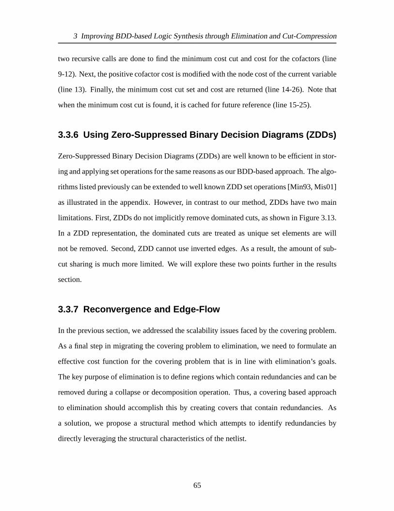
3 Improving BDD-based Logic Synthesis through Eliminationand Cut-Compression
two recursive calls are done to find the minimum cost cut and cost for the cofactors (line
9-12). Next, the positive cofactor cost is modified with the node cost of the current variable
(line 13). Finally, the minimum cost cut set and cost are returned (line 14-26). Note that
when the minimum cost cut is found, it is cached for future reference (line 15-25).
3.3.6 Using Zero-Suppressed Binary Decision Diagrams (ZDD s)
Zero-Suppressed Binary Decision Diagrams (ZDDs) are well known to be efficient in stor-
ing and applying set operations for the same reasons as our BDD-based approach. The algo-
rithms listed previously can be extended to well known ZDD set operations [Min93, Mis01]
as illustrated in the appendix. However, in contrast to our method, ZDDs have two main
limitations. First, ZDDs do not implicitly remove dominated cuts, as shown in Figure 3.13.
In a ZDD representation, the dominated cuts are treated as unique set elements are will
not be removed. Second, ZDD cannot use inverted edges. As a result, the amount of sub-
cut sharing is much more limited. We will explore these two points further in the results
section.
3.3.7 Reconvergence and Edge-Flow
In the previous section, we addressed the scalability issues faced by the covering problem.
As a final step in migrating the covering problem to elimination, we need to formulate an
effective cost function for the covering problem that is in line with elimination’s goals.
The key purpose of elimination is to define regions which contain redundancies and can be
removed during a collapse or decomposition operation. Thus, a covering based approach
to elimination should accomplish this by creating covers that contain redundancies. As
a solution, we propose a structural method which attempts toidentify redundancies by
directly leveraging the structural characteristics of thenetlist.
65

3 Improving BDD-based Logic Synthesis through Eliminationand Cut-Compression
In our analysis, we will focus on reconvergent paths to help isolate redundancies. A re-
convergent path is defined as a path that branches into two distinct paths which later merge
into a single path. Figure 3.18 illustrates two cones of logic: one without any reconvergent
paths, and one with reconvergent paths.
(a) Tree (b) Reconvergent
Figure 3.18: Illustration of cones with no reconvergent paths (a) and with reconvergentpaths (b).
Proposition 3.3.3 A cone of logic will have redundancies, only if it contains reconvergent
paths.
Proof: Proof by contradiction. Let’s assume that a cone of logic hasredundancies, but
contains no reconvergent paths. If a cone of logic contains no reconvergent paths, it forms
a tree structure. This implies that each node in the cone has exactly one path to a fanin to
the cone. If the cone has redundancies, this implies that oneof the nodes can be removed or
reduced (removal of one of the node inputs). However, if a node is removed or reduced, one
of the fanins of the cone will no longer have a path to the root of the cone, thereby changing
the function output from the root of the cone. Thus, the circuit has no redundancies and we
have a contradiction.�
By Proposition 3.3.3, when defining our covers we should isolate cones with reconver-
gent paths. In order to accomplish this, we use a heuristic cost function which attempts
to minimize the number of edges found within the final coveredgraph. This is ideal since
covers that contain reconvergent paths have less input edges than covers with no reconver-
66

3 Improving BDD-based Logic Synthesis through Eliminationand Cut-Compression
gent paths. Our cost function is referred to as edge flow,and by minimizing the overall edge
flow during covering selection, the total cut size of the finalcovering is minimized.
ef(Cv) =∑
u∈fanin(Cv)
ef(u) + W〈u,∗〉
| fanout(u) | (3.4)
ef(v) =MIN{ef(Cv) | Cv ∈ Φ(v)} (3.5)
Edge flow is defined recursively in Equation 3.4 and is denotedef( · ). The edge flow of
coverCv is defined as the sum of the edge flows of the fanin nodes toCv plus the weight
associated with each fanin edge〈u, ∗〉, W〈u, ∗〉. Here∗ is the head node for the fanin edge
of Cv. Also, for each fanin, we divide its edge flow summation by thesize of its fanout set.
The edge flow for a node is defined as the minimum cost edge flow ofany cover rooted at
nodev. If v is a primary input, its edge flow is defined as 0.
Under the general framework for the covering problem, the fanout size of a node will
not be known until the covering problem completes. For example, consider Figure 3.19.
If the covering chosen in the backward traversal is Figure 3.19a, nodev has a fanout of 2;
however, if the covering chosen is Figure 3.19b, the nodev has a fanout of 1. If the fanout
size can be estimated, edge flow can still be a good predictor of the resulting number of
edges in a given covering. The fanout size estimated can be found by taking a weighted
average of previous fanout sizes per node as shown in Equation 3.6 where| fanout(v)′ |est
is the estimate found in the previous iteration and| fanout(v) | is the actual number of
edges found in the last backward traversal. In cases wherev was not a cone root node in
the last covering chosen,| fanout(v) | is set to 1. On the first traversal,| fanout(v) |est is
set to the number of output edges of the nodev in the uncovered netlist. Previous reports
showed that settingα between 1.5 and 2.5 was best for iterations of 8 or less [MBV06].
67

3 Improving BDD-based Logic Synthesis through Eliminationand Cut-Compression
®(a) Two Fanouts
¯(b) One Fanout
Figure 3.19: Illustration of fanout dependency on the covering.
| fanout(v) |est=| fanout(v)′ |est +α | fanout(v) |
1 + α(3.6)
Figure 3.20: Equation for estimating a node’s fanout size.
3.4 Results
We empirically validate our analysis in the previous sections here. First, we create a BDD-
based cut generation algorithm, which we refer to asBddCut, and compare it to current
techniques. Next, we evaluate our edge flow heuristic when used to drive the covering
problem. Our last evaluation attempts to measure the benefits of the proposed covering
method under the context of a complete logic synthesis flow. To this end, we embed BddCut
as a replacement of the elimination procedure in FBDD, a BDD-based synthesis engine,
and evaluate its impact on runtime and area.
3.4.1 BddCut: Scalable Cut Generation
To evaluate our cut generation technique, we look at two aspects. Our first evaluation fo-
cuses on the scalability of the cut generation approach. Forevaluation, we compare our
68

3 Improving BDD-based Logic Synthesis through Eliminationand Cut-Compression
approach against two representative, state-of-the-art mappers: IMap, one of the earliest
mappers to use cut-generation for technology mapping; and ABC, the most recently re-
ported synthesis flow that employs a state-of-the-art cut generation algorithm for many of
its algorithms.
To investigate our symbolic approach to cut generation, we compare the cut generation
time of BddCut against IMap’s [MBV06] and ABC’s [MCB06b] cutgeneration time. Note
that during all flows, we generate all possible cuts (i.e. no pruning) of sizeK or less.
Table 3.1 and Table 3.2 shows detailed results for select circuits, followed by Table 3.3
and 3.4 with summarized results for the entire ITC and ISCAS89 benchmark suite. We also
show a peak memory use comparison between ABC and BddCut as shown in Table 3.5.
Finally, we compared BddCut with ABC for one of the largest IWLS circuits which is
shown in Table 3.6. In cases that the technology mapper ran out of memory, the circuit
time is marked as n/a.
K=6 (sec) K=7 (sec)Circuit BddCut IMap ABC BddCut IMap ABCC6288 0.20 40.64 0.52 0.67 660.76 5.66des 0.36 10.46 0.19 0.70 294.05 3.34i10 0.22 14.27 0.25 1.58 98.27 2.00b20 1.84 81.89 0.88 8.27 890.67 8.69b21 1.91 86.84 0.94 8.59 929.90 8.66b22_1 2.17 107.16 1.38 8.81 n/a 10.3s9234.1 0.11 3.96 0.13 0.33 38.32 0.75s38417 0.45 13.68 0.31 1.39 133.83 0.72s4863 0.11 19.27 0.11 0.36 269.07 0.84s1494 0.11 15.73 0.09 0.33 197.76 0.63Ratio Geomean 63x 0.83 225x 1.8x
Table 3.1: Detailed comparison of BddCut cut generation time against IMap and ABC.IMap could not run forK ≥ 8.
The results in the previous table clearly indicate that due to subcut sharing and redundant
cut removal, our symbolic approach scales better than traditional techniques where IMap
69
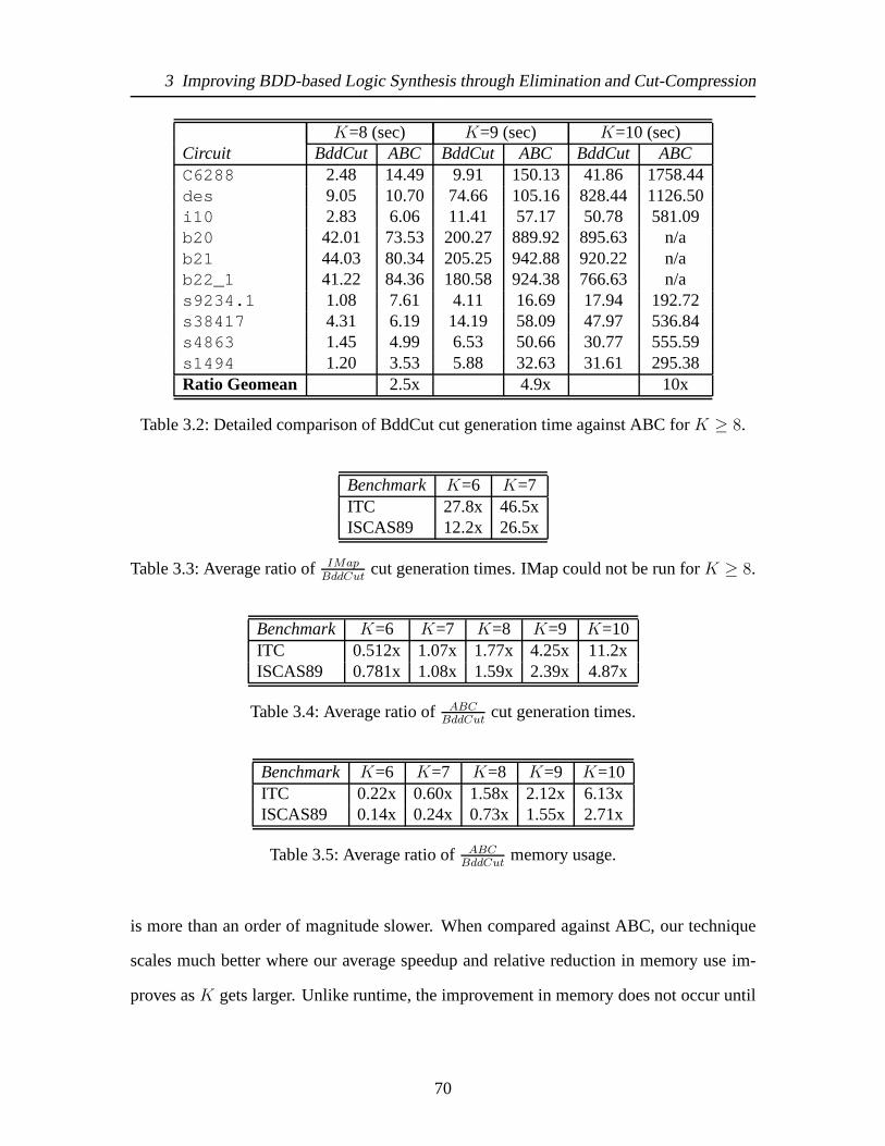
3 Improving BDD-based Logic Synthesis through Eliminationand Cut-Compression
K=8 (sec) K=9 (sec) K=10 (sec)Circuit BddCut ABC BddCut ABC BddCut ABCC6288 2.48 14.49 9.91 150.13 41.86 1758.44des 9.05 10.70 74.66 105.16 828.44 1126.50i10 2.83 6.06 11.41 57.17 50.78 581.09b20 42.01 73.53 200.27 889.92 895.63 n/ab21 44.03 80.34 205.25 942.88 920.22 n/ab22_1 41.22 84.36 180.58 924.38 766.63 n/as9234.1 1.08 7.61 4.11 16.69 17.94 192.72s38417 4.31 6.19 14.19 58.09 47.97 536.84s4863 1.45 4.99 6.53 50.66 30.77 555.59s1494 1.20 3.53 5.88 32.63 31.61 295.38Ratio Geomean 2.5x 4.9x 10x
Table 3.2: Detailed comparison of BddCut cut generation time against ABC forK ≥ 8.
Benchmark K=6 K=7ITC 27.8x 46.5xISCAS89 12.2x 26.5x
Table 3.3: Average ratio ofIMap
BddCutcut generation times. IMap could not be run forK ≥ 8.
Benchmark K=6 K=7 K=8 K=9 K=10ITC 0.512x 1.07x 1.77x 4.25x 11.2xISCAS89 0.781x 1.08x 1.59x 2.39x 4.87x
Table 3.4: Average ratio ofABCBddCut
cut generation times.
Benchmark K=6 K=7 K=8 K=9 K=10ITC 0.22x 0.60x 1.58x 2.12x 6.13xISCAS89 0.14x 0.24x 0.73x 1.55x 2.71x
Table 3.5: Average ratio ofABCBddCut
memory usage.
is more than an order of magnitude slower. When compared against ABC, our technique
scales much better where our average speedup and relative reduction in memory use im-
proves asK gets larger. Unlike runtime, the improvement in memory doesnot occur until
70

3 Improving BDD-based Logic Synthesis through Eliminationand Cut-Compression
runtime (sec) memory (GB)Cut Size BddCut ABC BddCut ABC
6 23.3 77.9 0.43 1.417 58.9 n/a 0.45 n/a8 152.9 n/a 0.60 n/a9 547.6 n/a 0.81 n/a
Table 3.6: Runtime comparison of BddCut with ABC on circuitleon2 (contains 278,2924-LUTs).
K gets large (K > 7). We found that because there is a fixed overhead in the CUDD
BDD manager [Som98], and therefore only at the larger cut sizes was this overhead amor-
tized through subcut sharing or if the benchmark is large as in the case ofleon2 shown
in Table 3.6. Without subcut sharing, memory runs out for a few of the larger benchmark
circuits whenK = 10. This is also true for extremely large benchmark circuits asshown in
Table 3.6 where ABC runs out of memory in circuitleon2 for K > 6. Fortunately, ABC
supports cut dropping which has proven to reduce the memory usage by several fold, but,
from our experience, cut dropping increases the cut computation time so we did not turn
on this feature. For example, with cut dropping enabled, ABCtook more than 12 hours to
generate 10-input cuts for circuitb20 , whereas BddCut takes less than 15 minutes.
Although ABC outperforms BddCut for small cut sizes, the longest 6-input cut gener-
ation time in BddCut was 2.8 seconds. For small cut sizes, theoverhead in storing and
generating BDDs is not amortized when generating cut sets symbolically, thus ABC is still
the better approach for smaller values ofK. The exception to this trend occurs for circuits
with a high degree of reconvergence such as for circuitC6288 (C6288 is a multiplier). For
these circuits, our relative speedup is much larger for all values ofK because reconvergent
paths dramatically increase the number of cut duplicationsin conventional cut generation
methods.
A concern one could raise with our symbolic approach is the effect of BDD representa-
tion of cuts on the cache. Since the CUDD package represents BDDs as a set of pointers,
71

3 Improving BDD-based Logic Synthesis through Eliminationand Cut-Compression
the nodes in each BDD may potentially be scattered throughout memory. Thus, any BDD
traversal would lead to cache thrashing, which would dramatically hurt the performance
of our algorithm. However, CUDD allocates BDD nodes from a continuous memory pool
leading to BDDs that exhibit good spatial locality. Our competitive results support this
claim and indicate that good cache behaviour is maintained with CUDD.
3.4.2 Edge Flow Heuristic
The new edge flow heuristic is used in the context of the covering problem for elimination.
Since in elimination attempts to capture reconvergent regions as described in Section 3.3.7,
our goal is to ensure that edge flow results in a graph with lessedges; however, we must
ensure that other metrics correlated to overall area and delay are not degraded. To do so,
we compare our edge flow based covering algorithm against a robust area driven covering
algorithm [MBV06]. The metrics we use to evaluate the resulting cover are the number of
resulting covers, the longest path of the resulting coveredgraph, and the resulting number
of edges in the graph. The resulting number of covers is important since this directly
correlates to the final area of the circuit. In a similar sense, the longest path correlates to
the final delay of the circuit.
Table 3.7 shows our results on the ITC and ISCAS89 benchmark set where only a few
circuits have been shown in detail. Three groups of columns are shown that compare the
number of covers (# Covers), longest path (Longest Path), and number of edges (# Edges) in
the resulting covered graph. The first column (af ) in each group lists the results of the area
driven flow, and the second column (ef ) in each group lists the results of the edge driven
flow. The edge flow heuristic has a clear impact on the final covered graph. Overall, edge
flow can reduce the overall number of edge in the final covered graph by 7% on average
with no impact to the area or delay of the final covered circuit. Interestingly these results
were also found successively in an independent study published in [JCCM08].
72
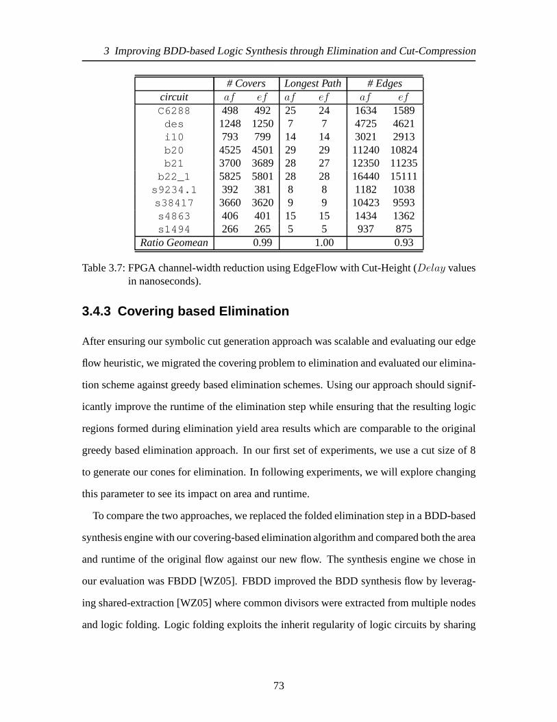
3 Improving BDD-based Logic Synthesis through Eliminationand Cut-Compression
# Covers Longest Path # Edgescircuit af ef af ef af efC6288 498 492 25 24 1634 1589
des 1248 1250 7 7 4725 4621i10 793 799 14 14 3021 2913b20 4525 4501 29 29 11240 10824b21 3700 3689 28 27 12350 11235
b22_1 5825 5801 28 28 16440 15111s9234.1 392 381 8 8 1182 1038s38417 3660 3620 9 9 10423 9593s4863 406 401 15 15 1434 1362s1494 266 265 5 5 937 875
Ratio Geomean 0.99 1.00 0.93
Table 3.7: FPGA channel-width reduction using EdgeFlow with Cut-Height (Delay valuesin nanoseconds).
3.4.3 Covering based Elimination
After ensuring our symbolic cut generation approach was scalable and evaluating our edge
flow heuristic, we migrated the covering problem to elimination and evaluated our elimina-
tion scheme against greedy based elimination schemes. Using our approach should signif-
icantly improve the runtime of the elimination step while ensuring that the resulting logic
regions formed during elimination yield area results whichare comparable to the original
greedy based elimination approach. In our first set of experiments, we use a cut size of 8
to generate our cones for elimination. In following experiments, we will explore changing
this parameter to see its impact on area and runtime.
To compare the two approaches, we replaced the folded elimination step in a BDD-based
synthesis engine with our covering-based elimination algorithm and compared both the area
and runtime of the original flow against our new flow. The synthesis engine we chose in
our evaluation was FBDD [WZ05]. FBDD improved the BDD synthesis flow by leverag-
ing shared-extraction [WZ05] where common divisors were extracted from multiple nodes
and logic folding. Logic folding exploits the inherit regularity of logic circuits by sharing
73

3 Improving BDD-based Logic Synthesis through Eliminationand Cut-Compression
transformations between equivalent logic structures. This has a huge impact on runtime
where it has been shown to reduce the number of elimination operations by 60% on aver-
age. We also compare against SIS for a common reference point. For ease of readability,
we will refer to our flow which uses covering-based elimination asFBDDnew. Starting
with unoptimized benchmark circuits, we optimized the circuits with FBDDnew, FBDD,
and SIS. To compare their area results, we technology mappedour optimized circuits to 4-
LUTs using the technology mapping algorithm described in [MBV06]. When optimizing
the circuits in SIS, we usedscript.rugged [ESV92]. Table 3.8 illustrates detailed results
for a few benchmark circuits. ColumnCircuit lists the circuit name, columnTime lists
the total runtime in seconds, and column4-LUT Arealists the 4-LUT count. Note a few
circuits caused SIS to run out of memory and are marked as n/a.The final row lists the
geometric mean of the ratio when compared againstFBDDnew.
Time (sec) 4-LUT AreaCircuit FBDDnew FBDD SIS FBDDnew FBDD SISb20 5.5 44.8 154.5 4514 4324 4773b21 7.9 35.8 185.1 3700 3689 3721b22_1 6.2 38.4 202.4 5788 6505 5664s38417 1.9 7.2 58.0 3560 3559 4052s38584 3.0 13.7 3927.3 4289 4152 4174s35932 3.9 4.1 n/a 3264 3360 n/as15850 0.8 9.1 68.8 1282 1270 1329systemcdes 3.1 11.3 123.1 1152 1207 1143vga_lcd 38.9 585.2 n/a 40680 40676 n/awb_conmax 18.6 104.2 1313.5 19135 19479 19726Ratio Geomean 5.7x 70x 1.00 1.03
Table 3.8: Detailed comparison of area and runtime ofFBDDnew against FBDD and SISfor K = 8. FBDDnew
FBDD or SIS
For the circuits shown in Table 3.8, our new flow is significantly faster than the original
FBDD with an average speedup of over 5x and an order of magnitude speedup over SIS.
The results also show that this speedup comes with no area penalty.
74
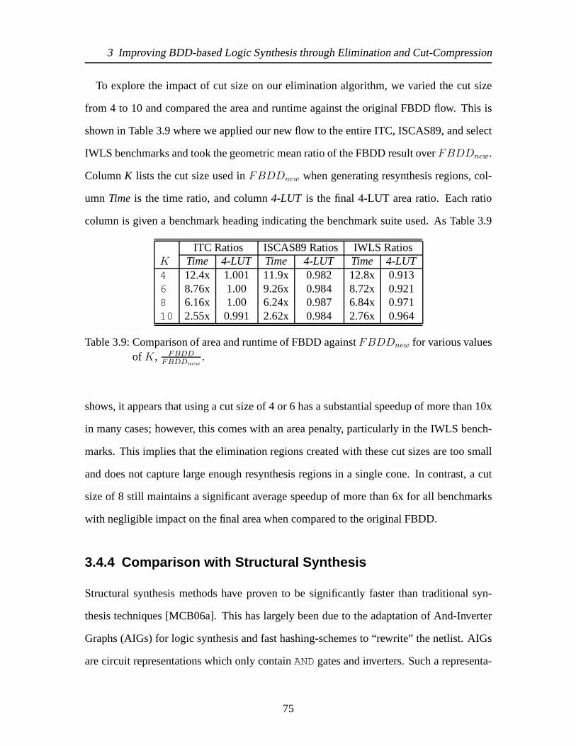
3 Improving BDD-based Logic Synthesis through Eliminationand Cut-Compression
To explore the impact of cut size on our elimination algorithm, we varied the cut size
from 4 to 10 and compared the area and runtime against the original FBDD flow. This is
shown in Table 3.9 where we applied our new flow to the entire ITC, ISCAS89, and select
IWLS benchmarks and took the geometric mean ratio of the FBDDresult overFBDDnew.
ColumnK lists the cut size used inFBDDnew when generating resynthesis regions, col-
umn Time is the time ratio, and column4-LUT is the final 4-LUT area ratio. Each ratio
column is given a benchmark heading indicating the benchmark suite used. As Table 3.9
ITC Ratios ISCAS89 Ratios IWLS RatiosK Time 4-LUT Time 4-LUT Time 4-LUT4 12.4x 1.001 11.9x 0.982 12.8x 0.9136 8.76x 1.00 9.26x 0.984 8.72x 0.9218 6.16x 1.00 6.24x 0.987 6.84x 0.97110 2.55x 0.991 2.62x 0.984 2.76x 0.964
Table 3.9: Comparison of area and runtime of FBDD againstFBDDnew for various valuesof K, FBDD
FBDDnew
.
shows, it appears that using a cut size of 4 or 6 has a substantial speedup of more than 10x
in many cases; however, this comes with an area penalty, particularly in the IWLS bench-
marks. This implies that the elimination regions created with these cut sizes are too small
and does not capture large enough resynthesis regions in a single cone. In contrast, a cut
size of 8 still maintains a significant average speedup of more than 6x for all benchmarks
with negligible impact on the final area when compared to the original FBDD.
3.4.4 Comparison with Structural Synthesis
Structural synthesis methods have proven to be significantly faster than traditional syn-
thesis techniques [MCB06a]. This has largely been due to theadaptation of And-Inverter
Graphs (AIGs) for logic synthesis and fast hashing-schemesto “rewrite” the netlist. AIGs
are circuit representations which only containANDgates and inverters. Such a representa-
75

3 Improving BDD-based Logic Synthesis through Eliminationand Cut-Compression
tion makes transformations on the netlist extremely fast where the netlist is locally updated
using rewriting which replaces 4-input logic functions within the netlist with an AIG repre-
sentation that either uses fewerANDgates or reduces the number of logic levels. Thus it is
generally accepted that structural AIG transformations are the fastest methods to perform
logic synthesis.
Table 3.10 shows a comparison of runtime and area between theABC logic synthesis
engine, a robust AIG-based synthesis flow, and our improved BDD-based synthesis flow
that uses a cut size of 8 during elimination. In the comparison, we use the resynthesis script
resyn2.rc to perform AIG rewriting and refactoring on the netlist and technology map
all circuits to 4-input LUTs.
ITC Ratios ISCAS89 Ratios IWLS RatiosTime 4-LUT Time 4-LUT Time 4-LUT1.31x 1.04 1.43x 1.01 1.28x 0.963
Table 3.10: Comparison of area and runtime of FBDD (K = 8) against AIG Rewrit-ing/Refactoring.
Overall, our results suggest that BDD-based synthesis flowsstill cannot beat AIG-based
flows using structural logic synthesis in terms of runtime. However, for larger benchmarks
found in the IWLS benchmark suite, we have a slight area advantage. Since we have shown
that we can reduce the synthesis flow runtime to an order of minutes, a 28% overhead in
terms of runtime translates to a few minutes, which in many cases is an acceptable amount
of runtime penalty when improving area. This shows that BDDsand structural techniques
can play a complementary role in optimizing netlists for logic synthesis.
76

3 Improving BDD-based Logic Synthesis through Eliminationand Cut-Compression
3.5 Summary
In this chapter we described a methodology for improving theruntime of BDD-based logic
synthesis flows by 6x with a negligible impact to the final circuit area. This speedup was
achieved by adapting the covering problem to elimination byintroducing a novel edge flow
heuristic to reduce the number of edges found in a logic circuit along with a BDD-based
compression technique to store and process cuts. Our results show that our edge flow
heuristic can reduce the number of edges within a circuit by 7% on average, while our
BDD-based compression technique was shown to reduce the cutgeneration runtime and
memory use by an order of magnitude.
77

4 Budget Management for Partitioning
Partitioning has become a popular means to manage scalability problems of existing CAD
algorithms. This is attractive since partitioning a circuit can dramatically reduce the solu-
tion space of the original problem, and hence improve its runtime. In the context of logic
synthesis, this involves partitioning the netlist followed by applying logic optimizations to
each partition. An example of a partitioned circuit is shownin Figure 4.1 which shows six
partitions highlighted in the dashed lines.
Figure 4.1: Partitioning of circuit for resynthesis.
In a partitioned circuit, each partition is optimized individually. For example, Fig-
78

4 Budget Management for Partitioning
ure 4.2(a) illustrates a depth optimization on an individual partition where the partition
depth is reduced. This optimized partition is then insertedback into the original circuit as
shown in Figure 4.2(b). By optimizing the depth of each partition, the overall circuit depth
has been reduced from 12 to 10 as highlighted by the shaded basic gates.
In the previous example, we were able to reduce the depth of the overall circuit by
optimizing each individual partition optimally. However,an optimal decomposition for
a circuit partition may not necessarily be the best decomposition when looking at the entire
circuit. For example, in the previous figure, the optimal depth decomposition of a partition
is shown in Figure 4.2(a). However, if a non-optimal skewed decomposition is used, as
shown in Figure 4.3(a), an improved global circuit depth of 8is achievable as shown in
Figure 4.3(b).
The previous example highlights that optimizations which may be beneficial from a sub-
circuit’s perspective may actually lead to a poor global result. One possible solution to this
is to apply incremental updates to the circuit, where partitions are individually optimized
in an iterative fashion. However, this requires several static timing iterations, which can
significantly hurt the runtime benefits of partitioning. Furthermore, a “ping-pong” prob-
lem can occur where paths are consistently over or under-optimized between iterations. To
avoid these problems, circuit constraints should be applied to all the partitions in a single
shot. In addition to removing the iterative nature of incremental approaches, this allows the
resynthesis engine to produce skewed decompositions as shown in Figure 4.3(a).
In this chapter we create partition constraints to improve the circuit depth with minimal
impact to the final circuit area. When applied to depth optimizations, the circuit constraint
we seek is known as the depth budget, which is a numeric value assigned to each partition
input. The depth budget for each input lists the maximum depth allowable between the
given input and root node in order to achieve some global depth value. This is beneficial for
two reasons. First, it indicates which input paths in a givenpartition must be “shortened”
79

4 Budget Management for Partitioning
(a)
(b)
Figure 4.2: Retransformation optimization to shorten the critical path using a localizedview of each partition. Original depth of circuit in Figure 4.2 is 12, final depthis 10 along shaded gates.
80

4 Budget Management for Partitioning
(a)
(b)
Figure 4.3: Retransformation optimization to shorten the critical path using budget con-straints to guide optimizations in each partition. Final depth is 8.
81

4 Budget Management for Partitioning
in order to improve the overall circuit depth. Second, it gives flexibility to input paths to
focus its circuit optimizations on area, as opposed to circuit depth. An illustration of this is
shown in Figure 4.4, which shows how we can achieve the skeweddecomposition shown
previously using depth budgets assigned to each partition inputs. In Figure 4.4, input paths
that are assigned a relatively large depth budget (6 in this case) can be optimized for area,
while input paths assigned small depth budgets (2 in this case) must be optimized for depth.
°°±± ²² ±±
Figure 4.4: Illustration of numericdepth budgetassignments to each partition input.
In this chapter, we show that the problem of deriving effective budget constraints as high-
lighted in Figure 4.4 can be formulated as an Integer-LinearProgram (ILP). By following
the constraints found from the ILP, the resulting optimizedcircuit has a superior Quality
of Result (QoR) to that of one with only a localized view of thepartition.
It is well known that the ILP problem is NP-complete [CLRS01]and, thus, solving
our budgeting problem as an ILP will not scale to large circuits requiring a large number
of constraints. To resolve this issue, we show later in Section 4.2.2 how we can reduce
82

4 Budget Management for Partitioning
our ILP to polynomial complexity by leveraging the concept of duality. Note that in this
chapter, the term duality is used in the context of convex optimization theory, and has no
relation to the definition of thedual of a logic functionfound in Boolean algebra. Doing so
reduces the problem runtime by over 100x, which is a necessary condition for our technique
to be practical for large circuits. Furthermore, although our reduced problem theoretically
has a polynomial complexity with respect to circuit size, empirically we find that it runs
in linear time on average. When run on the IWLS benchmark set,we show that our ILP
formulation can assist partition based logic synthesis which improves circuit depth by 11%
on average with a less than 1% penalty to area when compared against partitioning-based
flows without budgeting.
The rest of the chapter is organized as follows: Section 4.1 gives some background infor-
mation on the budget management problem; Section 4.2 illustrates our budget management
scheme in the context of logic synthesis and how we reduce itscomplexity to polynomial
time using duality; Section 4.3 highlights our results; andSection 4.4 concludes the chapter.
4.1 Background and Previous Work
4.1.1 Budget Management
Budget management is a common problem found in all steps of the FPGA CAD flow. It is
the problem of judiciously setting circuit constraints on local regions within a circuit while
providing enough freedom to optimize for other characteristics of the circuit [BGTS04,
LXZ07]. Furthermore, these local constraints must be set toensure that the global con-
straints of the entire circuit are also met. The difficulty ofbudget management arises when
various circuit characteristics work in opposition to eachother. For example, circuit area
and power have an inverse relationship to circuit depth and performance and choosing be-
tween alternate design implementations is often a trade-off between these characteristics.
83

4 Budget Management for Partitioning
An example of the budget management problem is found in [GBCS04] which works
on improving the resulting area of a circuit during high-level synthesis. During high-level
synthesis, the circuit is represented as a data-flow graph (DFG) where each node repre-
sents a functional operation (e.g. addition or multiplication). Choosing between various
implementations of each node involves a trade-off between clock-cycle latency and area.
In [GBCS04], clock-cycle latency is define as the number of clock cycles required to com-
plete a computation; this has a big impact on the final area of the circuit. For example,
for a given clock period, the area of a single-cycle multiplier is significantly higher than
to that of a multi-cycle multiplier. The problem of budget management deals with how to
choose between such alternatives of each DFG node such that the overall area is minimized
while maintaining the latency, in terms of clock cycles, of the entire circuit. An example
of this is shown in Figure 4.5 which shows two implementations of the same sequential
circuit. In Figure 4.5, each node represents a functional unit such as a multiplier and is
labeled with two numbers. The top number lists the latency ofthe node and the bottom
lists its area units. For the two DFGs shown, the latency is 7 (i.e. there are 7 registers along
every path from any input to output). In Figure 4.5(a), the total area is 84. Assuming that
the bottom most node will have a significant area savings if replaced with a 2-cycle unit,
the total circuit area can be reduced if an additional cycle is allocated to the bottom most
node. However, in order to maintain a circuit latency of 7, wemust obtain this additional
cycle from one node along each path which the bottom node belongs to as shown in Fig-
ure 4.5(b). In our case, we moved one cycle from the two nodes feeding into the top most
node (4-cycle unit replaced by a 3-cycle unit, and a 3-cycle unit is replaced with a 2-cycle
unit).
As the previous example illustrate, clock cycles should be assigned to nodes which can
best leverage the additional clock cycles to reduce its area. This is difficult since each
DFG node has a unique clock latency versus area trade-off curve. Thus, greedy heuristic
84

4 Budget Management for Partitioning
³́µ ¶µ³µ·
µ́¸µ́¸¹º» ¼½¾¿ÀÁºÂÃÄ¿Å Æ ÇȾº½ ÉÊú Æ ·³
(a)
ËÌË ÍÍÎÍÏ
ÌÍÐÍÌÍÑÒÓ ÔÕÖ×ØÙÒÚÛÜ×Ý Þ ßàÖÚÒÕ áâÛÒ Þ ßã
(b)
Figure 4.5: Alternate implementations of the same circuit,each node with a different circuitlatency allocated to it.
approaches often lead to missed opportunities to reduce circuit area. As an alternative, the
authors in [GBCS04] formulate this problem as a convex optimization problem. The results
of their budget management is significant where they are ableto reduce the overall FPGA
LUT usage of their design by 29% without changing the latencyof the final circuit.
From a budgeting perspective, our work is similar. However,in our case, we are dealing
with logic depth as our main budgeting constraint, as opposed to clock cycles.
4.2 Partitioning with Delay Budgeting
During logic synthesis, the primary goal is to minimize the circuit area, while reducing the
depth of the circuit. Achieving these goals after partitioning is significantly more difficult
since the critical path cannot be identified by looking at each partition individually. Fur-
thermore, even if the critical path information is annotated prior to partitioning, optimizing
each path in isolation can cause problems where paths are “over-optimized” for depth while
“under-optimized” for area. This chapter addresses these problems through budget man-
85

4 Budget Management for Partitioning
agement which annotates each partition with information tohelp guide the optimizer. This
approach has four primary steps as follows:
• A clustering algorithm to partition the netlist into disjoint partitions.
• A fast conversion of the circuit to an And-Inverter Graph (AIG), which is neces-
sary to help model the area-delay relationship of each partition used in the budget
management formulation.
• A budgeting algorithm to allocate a fair distribution of budget to the partition inputs.
• A resynthesis algorithm that can utilize the budgeting information to drive a delay
driven resynthesis engine.
4.2.1 Partitioning and AIG construction
To partition the circuit, we apply a variant of the covering problem which attempts to
minimize the number of edges found between partitions. The resulting circuit will be a
set of covers where each cover encapsulates a localized region of the circuit. A simplified
illustration of the partitioning phase is shown in Figure 4.6 and is described in detail in
Chapter 3. In Figure 4.6(b), partition regions are highlighted, which are then represented
as a single node in Figure 4.6(c). Although only small partitions are shown in this example,
larger partitions which can have more than 10 inputs are usedin this work.
After partitioning, each partition is converted to an And-Inverter Graph (AIG). An AIG
is a circuit representation which consists of only 2-inputANDgates and inverters as illus-
trated in Figure 4.7. Here, we represent inverters as “bubbles” on a given graph edge. The
benefit of this construction is that it unifies the representation of the entire circuit, which
makes resynthesis extremely fast and simple [MCB06a]. To generate the AIG, we first
convert the logic function for each node in the circuit into an irredundant sum-of-product
86

4 Budget Management for Partitioning
(a) (b) (c)
Figure 4.6: Clustering of a simple netlist. (a) Original netlist (b) Partitioning of originalnetlist (c) Representing each partition and PI as a single node
form (ISOP). An ISOP is a Boolean expression that contains noredundant cubes in the
expression. Following this, the ISOP for each node is factored to reduce its cost. This
simplified Boolean expression is then converted directly into a network of AND gates and
inverters [MCB06a]. We will show in later sections that the AIG structure will help us
express the area-delay relationship of each partition usedin our budgeting formulation.
f g
Figure 4.7: Example of an And-Inverter Graph (AIG) where each node is a 2-inputANDgate and each edge can be inverted.
4.2.2 Budget Management
Following partitioning and AIG construction, each partition must be annotated with in-
formation to guide the succeeding resynthesis step. Duringresynthesis the two primary
87

4 Budget Management for Partitioning
optimization metrics are area and depth where we seek to minimize both. However, since
in general area and depth are conflicting optimization parameters there exists a trade-off
decision where partitions that are optimized for area usually increase in depth. Thus, the
question that must be answered when resynthesizing each partition is as follows: what is
the maximum tolerable increase in depth for each partition without violating a given over-
all circuit depth constraint? We seek to maximize the depth of each partition since this
allows for more opportunities in area reduction. The inverse relationship between area and
depth is illustrated in Figure 4.8 where Figure 4.8(a) illustrates the circuit implementation
when area, in terms of gate count, is minimized while Figure 4.8(b) illustrates the circuit
implementation when delay, in terms of logic levels, is minimized at the cost of area.
f g
(a)
f g
(b)
Figure 4.8: Illustration of circuit optimization for 4.8(a) area (gate-count=4, logic-levels=4)and 4.8(b) depth (gate-count=7, logic-levels=3).
The question raised previously can be rephrased more formally as a budget management
problem stated as follows:
Problem 4.2.1 Delay Budgeting Problem. Given a partitioned circuit and a required delay
Dreq of the circuit measured in terms of circuit depth, allocate adelay budget on each
partition input such that the resulting delay on any given path is less than or equal toDreq
and the estimated total circuit area is minimized.
By solving Problem 4.2.1, a delay budget will be assigned to each partition input to give
88

4 Budget Management for Partitioning
guidance on resynthesis optimization. For example, referring to Figure 4.9, a delay budget
assignment is given to each partition input. These assignments act as an upper-bound on
depth for the resynthesis engine to follow. This results in afinal circuit implementation, as
shown previously in Figure 4.3, that has improved depth overa non-budgeted flow, even
though locally the resulting circuit appears to be sub-optimal in terms of circuit depth. Note
that we use depth as a measure of delay since at the logic synthesis level, accurate delay
information of each edge is not available.
ääåå ææ åå
Figure 4.9: Annotated partition inputs after delay budgeting.
In order to model Problem 4.2.1, we must first model the delay-area relationship of each
partition. For simplicity, we model the delay-area relationship as a piecewise-linear convex
function with respect to the depth budget,bij . Herei is the label assigned to the partition
whose output feeds into the partitionj. For every partition input, there is a depth budget
variable,bij . In the convex function, we measure delay in terms of logic levels, and area
in terms of gate count. Finally, we apply a lower and upper bound on the delay constraint
([L, U ]), since for any given partition, there will exist a minimum and maximum total depth
89

4 Budget Management for Partitioning
achievable by that partition. This relationship is illustrated in Figure 4.10 which shows
the piecewise-linear convex functionFij(bij). Here,bij is the depth budget, measured in
terms of logic levels, andFij(bij) is the estimate of area along the given path. Later, in
Section 4.2.2 we will illustrate how we derive the area-delay relationship,Fij(bij), in more
detail.
0
2
4
6
8
10
12
14
L M U
b ij
F( b
ijij
)
Figure 4.10: Simplified inverse relationship between delaybudget,bij , and area estimation,Fij(bij), defined over variablebij .
If we assume that the area and delay values take on integer values and that there exists
an area-delay relationship along each input of the partition, we can represent Problem 4.2.1
90
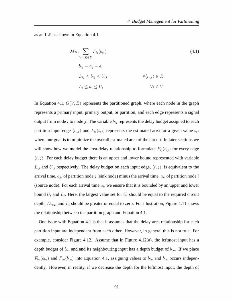
4 Budget Management for Partitioning
as an ILP as shown in Equation 4.1.
Min∑
∀〈i,j〉∈E
Fij(bij) (4.1)
bij = aj − ai
Lij ≤ bij ≤ Uij ∀〈i, j〉 ∈ E
Li ≤ ai ≤ Ui ∀i ∈ V
In Equation 4.1,G(V, E) represents the partitioned graph, where each node in the graph
represents a primary input, primary output, or partition, and each edge represents a signal
output from nodei to nodej. The variablebij represents the delay budget assigned to each
partition input edge〈i, j〉 andFij(bij) represents the estimated area for a given valuebij
where our goal is to minimize the overall estimated area of the circuit. In later sections we
will show how we model the area-delay relationship to formulateFij(bij) for every edge
〈i, j〉. For each delay budget there is an upper and lower bound represented with variable
Lij andUij respectively. The delay budget on each input edge,〈i, j〉, is equivalent to the
arrival time,aj , of partition nodej (sink node) minus the arrival time,ai, of partition nodei
(source node). For each arrival timeai, we ensure that it is bounded by an upper and lower
boundUi andLi. Here, the largest value set forUi should be equal to the required circuit
depth,Dreq, andLi should be greater or equal to zero. For illustration, Figure4.11 shows
the relationship between the partition graph and Equation 4.1.
One issue with Equation 4.1 is that it assumes that the delay-area relationship for each
partition input are independent from each other. However, in general this is not true. For
example, consider Figure 4.12. Assume that in Figure 4.12(a), the leftmost input has a
depth budget ofbba and and its neighbouring input has a depth budget ofbca. If we place
Fba(bba) andFca(bca) into Equation 4.1, assigning values tobba and bca occurs indepen-
dently. However, in reality, if we decrease the depth for theleftmost input, the depth of
91

4 Budget Management for Partitioning
j
k
i
bçè=aè -aç=3
bè é=aé-aè=2aé=5
aè=3
aç=0
Fè é(bè é)=Fè é(2)=6
Fçè (bçè )=Fçè (3)=5
2 < bçè < 5
2 < bè é < 50 < aé < 5
0 < aè < 5
0 < aç < 5
Figure 4.11: Graph to ILP formulation.
its neighbouring input must also decrease. Thus variablesbba andbca are related. Adding
this dependency to our problem significantly increases its complexity and for simplicity we
ignore this dependency. In later sections we empirically evaluate this simplification and
show in practice that it is not an issue.
f g
êëì êíì(a)
f g
îïð îñð(b)
Figure 4.12: Illustration of dependency of depth between inputs.
Reduction of ILP using Duality
Once we formulate Equation 4.1, we can use any standard ILP solver to derive a depth
budget,bij , for every edge〈i, j〉 in the graph. However, solving our ILP problem directly
92

4 Budget Management for Partitioning
is not scalable to large designs. To avoid solving our objective function directly, we should
attempt to reduce the complexity of our problem. Previous works [BGTS04, LXZ07] have
shown that in certain cases, an ILP can be reduced to a form which has a much simpler com-
plexity. These techniques are often based around the notionof convexity and duality where
a dual functionof the original objective function is used as the primary objective function.
If it turns out that the original objective function is convex, finding the optimal solution
to the dual function yields a result which is equivalent to the optimal value of the original
function. Since in Equation 4.1 we assumed thatFij(bij) is convex (linear or piecewise lin-
ear convex) for all edges〈i, j〉, it can be shown that∑
∀〈i,j〉∈E
Fij(bij) is also convex [BV04].
An example of convex dual problems whose optimal solutions are equivalent is the min-cut
max-flow problem. The min-cut problem finds the capacity along the minimum cut within
a network of pipes and is equivalent to the max-flow problem that finds the maximum flow
along the same network of pipes. This min-max relationship is a common characteristic
of dual functions where a minimization problem for a given functionf(a) is converted to
a maximization problem for a dual functiong(λ), andMin f(a) ≡ Max g(λ). Also, in
general there does not exist a functionG whereλ = G(a) which implies that a solution
in a generally does not have an relationship to a solution inλ [BV04]. It should be noted
that in general, the dual function of a given function may notbe simpler to solve, but we
will show in this section that for our specific problem, usingthe dual function proves to be
significantly more scalable than solving the problem in its native ILP form.
To solve a problem using duality, several steps must be taken. First, the original convex
function must be converted to its dual function. When converting a convex function to its
dual, the original optimization variables are “removed” where a new set of optimization
variables are introduced. These new variables are known asLagrangian multipliers. Once
the dual function is derived, the optimal values of the Lagrangian multipliers are found.
Finally, the dual solution must be mapped back to the original problem space to derive
93
4 Budget Management for Partitioning
the optimal values on the original optimization variables.For example, referring back to
the min-cut max-flow problem, optimizing for the max-flow problem results in a solution
λ∗, which can be mapped to a solutiona∗ in the min-cut solution space. The remainder
of this section will describe these steps in detail, though the reader may skip directly to
Section 4.2.3 if not interested in the mathematical derivation. For those not familiar with
the concept of duality in the context of convex optimizations, it is recommended to review
duality in [BV04, ch.5].
When converting Equation 4.1 to its dual, we can assume that all our problem variables
and constraints are integers as shown in Equation 4.2.
bij , Uij, Lij ∈Z ∀〈i, j〉 ∈ E (4.2)
ai, Ui, Lj ∈Z ∀i ∈ V
Also, to simplify the derivation, we will assume that each function Fij(bij) is a linear
functionWijbij as shown in Equation 4.3. Later on, we will show how we will break this
assumption to accommodate more general forms forFij(bij).
Min∑
∀〈i,j〉∈E
Wijbij (4.3)
bij = aj − ai
Lij ≤ bij ≤ Uij ∀〈i, j〉 ∈ E
Li ≤ ai ≤ Ui ∀i ∈ V
Wij ∈ Z ∀〈i, j〉 ∈ E
In order to formulate the dual of Equation 4.3, we must first reformulate the function
to remove theai constraints on the second last line and represent the objective function
94

4 Budget Management for Partitioning
∑
∀〈i,j〉∈E
Wijbij in terms of node variables (currently it is a summation of theedge variables
bij). We can remove the constraintLi ≤ ai ≤ Ui by creating a dummy node 0 and attaching
each nodei to this dummy node. Next, we will map everyai variable to ab0i variable. Thus,
the resulting formulation remains the same, whereW0i = 0 for all i ∈ V . Following this,
we will remove all variablesbij and replace them with their equality constraintbij = aj−ai.
This leads to Equation 4.4.
Min∑
∀〈i,j〉∈E
Wij(aj − ai) (4.4)
aj − ai ≤ Uij ∀〈i, j〉 ∈ E
aj − ai ≥ Lij ∀〈i, j〉 ∈ E
Following the removal of thebij variables,∑
∀〈i,j〉∈E
Wijbij can be reexpressed in terms of
node variables only as shown in Equation 4.5 [LS91].
∑
∀〈i,j〉∈E
Wij(aj − ai) =∑
∀i∈V
(∑
∀〈k,i〉∈E
Wki −∑
∀〈i,j〉∈E
Wij)ai
(4.5)
=∑
∀i∈V
σiai (4.6)
σi =∑
∀〈k,i〉∈E
Wki −∑
∀〈i,j〉∈E
Wij
Substituting Equation 4.5 into Equation 4.4 leads to Equation 4.7. Simplifying the con-
95

4 Budget Management for Partitioning
straints to a standardized form is shown in Equation 4.8
Min∑
∀i∈V
σiai (4.7)
aj − ai ≤ Uij ∀〈i, j〉 ∈ E
aj − ai ≥ Lij ∀〈i, j〉 ∈ E
Min∑
∀i∈V
σiai (4.8)
aj − ai − Uij ≤ 0 ∀〈i, j〉 ∈ E
ai − aj + Lij ≤ 0 ∀〈i, j〉 ∈ E
Once Equation 4.8 is formed, we are ready to find its dual function. First, we remove
the constraints onai by using Lagrangian multipliers. Lagrangian multipliers remove con-
straints on an objective function by introducing new variables, known as Lagrangian mul-
tipliers, and multiplying these variables by the constraints. In our case, our Lagrangian
multipliers areλij andρij which creates a new objective functionL(ai, λij, ρij). Assum-
ing that the Lagrangian multipliers are positive integers,they can be thought as a penalty
factor which penalizes the objective functionL(ai, λij , ρij) whenever the constraints on the
original objective function are not met. As a result, findinga validai, λij, ρij assignment
that minimizesL(ai, λij , ρij) is equivalent to finding a validai that minimizes the original
objective function.
L(ai, λij, ρij) =∑
∀i∈V
σiai +∑
∀〈i,j〉∈E
λij(aj − ai − Uij) +∑
∀〈i,j〉∈E
ρij(ai − aj + Lij) (4.9)
Although minimizingL(ai, λij , ρij) will find us a validai assignment, this is not use-
ful since the complexity of minimizingL(ai, λij, ρij) is equally as difficult as solving the
96

4 Budget Management for Partitioning
original objective function. Instead, we willimfimizeout theai variables inL(ai, λij , ρij).
This significantly reduces the complexity of our problem since the resulting function will
be dependent only on variablesλij andρij and we no longer have to search for a solution
in the domain ofai.
To imfimizeai fromL(ai, λij , ρij), we will take theinfimumof L(ai, λij, ρij) with respect
to variableai. The infimum of a function with respect to a variablex is defined as the
greatest lower bound over the function over the domain ofx. For example, Table 4.1 shows
the infimum of several well known functions. Note that the infimum of the third and fourth
function is also another function dependent on the remaining variables.
f(x) infx∈D
f(x)
ex 0x2 + 2 2x2 + y y
y ymx + b, {m, b} ∈ constant, m 6= 0 −∞
n∑
i=0
mixi + bi, ∀i {mi, bi} ∈ constant, mi 6= 0 −∞
Table 4.1: Infimum of several functions
To derive the infimum ofL(ai, λij, ρij) with respect toai, we first separate out parts of
L(ai, λij, ρij) that are not dependent onai as shown in Equation 4.10. In Equation 4.11, we
only show the terms dependent onai. These form a summation of linear functionsmai + b,
wherem is equivalent toρi or λij, andb = 0. From Table 4.1, the infimum of a summation
of linear functions is−∞ 1. However, as indicated in Table 4.1, there is one condition
where the infimum is well defined (i.e. not−∞). This occurs if∑
∀i∈V
σiai +∑
∀〈i,j〉∈E
λij(aj−
ai) +∑
∀〈i,j〉∈E
ρij(ai − aj) is constant zero (this is equivalent to the condition∀i mi = 0 in
the last entry in Table 4.1), which in turn implies that Equation 4.11 evaluates to constant
1The sum of a set of linear functions is known as anaffinefunction
97
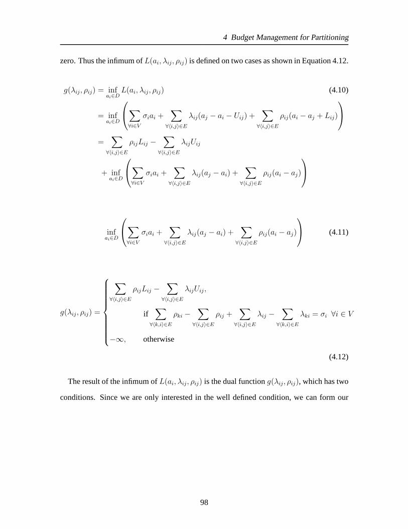
4 Budget Management for Partitioning
zero. Thus the infimum ofL(ai, λij, ρij) is defined on two cases as shown in Equation 4.12.
g(λij, ρij) = infai∈D
L(ai, λij, ρij) (4.10)
= infai∈D
∑
∀i∈V
σiai +∑
∀〈i,j〉∈E
λij(aj − ai − Uij) +∑
∀〈i,j〉∈E
ρij(ai − aj + Lij)
=∑
∀〈i,j〉∈E
ρijLij −∑
∀〈i,j〉∈E
λijUij
+ infai∈D
∑
∀i∈V
σiai +∑
∀〈i,j〉∈E
λij(aj − ai) +∑
∀〈i,j〉∈E
ρij(ai − aj)
infai∈D
∑
∀i∈V
σiai +∑
∀〈i,j〉∈E
λij(aj − ai) +∑
∀〈i,j〉∈E
ρij(ai − aj)
(4.11)
g(λij, ρij) =
∑
∀〈i,j〉∈E
ρijLij −∑
∀〈i,j〉∈E
λijUij ,
if∑
∀〈k,i〉∈E
ρki −∑
∀〈i,j〉∈E
ρij +∑
∀〈i,j〉∈E
λij −∑
∀〈k,i〉∈E
λki = σi ∀i ∈ V
−∞, otherwise
(4.12)
The result of the infimum ofL(ai, λij, ρij) is the dual functiong(λij, ρij), which has two
conditions. Since we are only interested in the well defined condition, we can form our
98

4 Budget Management for Partitioning
dual problem of the original ILP in Equation 4.1 as follows:
Max∑
∀〈i,j〉∈E
ρijLij −∑
∀〈i,j〉∈E
λijUij (4.13)
∑
∀〈k,i〉∈E
ρki −∑
∀〈i,j〉∈E
ρij +∑
∀〈i,j〉∈E
λij −∑
∀〈k,i〉∈E
λki = σi ∀i ∈ V
If we negate the objective function in Equation 4.13, the problem becomes a cost mini-
mization network flow algorithm where the dual variablesλij andρij are equivalent to the
flow along each edge〈i, j〉, Uij and−Lij represents the cost per unit flow on each edge,
andσi represents the flow demand on each nodei. This is shown in 4.14 and whose optimal
solution can be found in polynomial time [GT86, Gol97].
Min∑
∀〈i,j〉∈E
λijUij −∑
∀〈i,j〉∈E
ρijLij (4.14)
∑
∀〈k,i〉∈E
ρki −∑
∀〈i,j〉∈E
ρij +∑
∀〈i,j〉∈E
λij −∑
∀〈k,i〉∈E
λki = σi ∀i ∈ V
An illustration of the mathematical transformation described previously is shown in Fig-
ure 4.13. Figure 4.13(a) shows the original partition graphwhere each node represents a
partition and each edge represents connections between partitions. Figure 4.13(b) illus-
trates the converted graph with upper and lower bound constraints. Also, we show the
addition of the dummy nodev0 which is necessary to handle theai ≤ Ui constraints. For
clarity, we have shown this for only the top node.
Mapping dual variables to ai solution
Solving Equation 4.14 finds an optimal assignments to variablesλij andρij . However, our
original objective function seeks an optimal assignment tovariablesai. Thus, we must map
the optimal solutionλ∗ij andρ∗
ij in the dual solution space to the optimal solutiona∗i of the
99

4 Budget Management for Partitioning
(a)
5/-1
vò5/- 15 /-1
3/-1 5/ -1
3/-1
2 / -1
-5
2/-1
0 0
(b)
Figure 4.13: Graphical illustration of transforming the budget management problem into itsdual network flow problem. (a) Partitioned graph. (b) Upper and lower boundadded as edges to create network flow graph.
original objective function. In order to do this, we leverage the concept of complementary
slackness. This is stated in Proposition 4.2.2.
Proposition 4.2.2 Complementary slackness implies that for an optimal assignment toλ∗ij
andρ∗ij Equation 4.15 must hold.
λ∗ij(a
∗j − a∗
i − Uij) = 0, ∀〈i, j〉 ∈ E (4.15)
ρ∗ij(a
∗i − a∗
j + Lij) = 0, ∀〈i, j〉 ∈ E
Proof: Equation 4.15 is proven in Equation 4.16 [BV04, ch.5]. The first line states that
the optimal value of the original objective function is equal to the optimal value of its dual.
This is already assumed to be true from understanding duality for convex functions. The
second line is simply the definition of the dual function in expanded form, which is defined
as the infimum of the Lagrangian function with respect toai. The next inequality states
that the infimum will always be less than or equal to any value of the Lagrangian. This is
100

4 Budget Management for Partitioning
true since the infimum by definition is always less than its function (i.e. the greatest lower
bound). Finally, the last line states that the Lagrangian terms will always be less than or
equal to zero, and as a result, the Lagrangian will always be less than or equal to the original
objective function. Since the last line is equivalent to theoriginal objective function, this
implies thatλ∗ij(a
∗j − a∗
i − Uij) = 0 andρ∗ij(a
∗i − a∗
j + Lij) = 0 for all 〈i, j〉 ∈ E.
∑
∀i∈V
σia∗i = g(λ∗
ij, ρ∗ij) (4.16)
= infai∈D
∑
∀i∈V
σiai +∑
∀〈i,j〉∈E
λ∗ij(aj − ai − Uij) +
∑
∀〈i,j〉∈E
ρ∗ij(ai − aj + Lij)
≤∑
∀i∈V
σia∗i +
∑
∀〈i,j〉∈E
λ∗ij(a
∗j − a∗
i − Uij) +∑
∀〈i,j〉∈E
ρ∗ij(a
∗i − a∗
j + Lij)
≤∑
∀i∈V
σia∗i
�
The complementary slackness condition in Equation 4.15 is useful since it gives a rela-
tionship of eachai variable as shown in Equation 4.17.
∀〈i, j〉 ∈ E a∗j − a∗
i =
Uij, ifλ∗ij > 0
Lij , ifρ∗ij > 0
(4.17)
A problem with Equation 4.17 is that ifρ∗ij > 0 andλ∗
ij > 0, a∗j − a∗
i is undefined.
However, we can prove that such a condition is impossible in the following:
Proposition 4.2.3 If λ∗ij andρ∗
ij is the minimum cost solution to Equation 4.14, thenλ∗ij ×
ρ∗ij = 0, ∀〈i, j〉 ∈ E.
Proof: We know that assignmentsλ∗ij andρ∗
ij provide the solution to objective function in
Equation 4.14 with a minimum cost value ofM . Now assume that for a given edge〈i, j〉,
101

4 Budget Management for Partitioning
λ∗ij × ρ∗
ij 6= 0. This implies that there exists another feasible flow whereλij = λ∗ij − 1
andρij = ρ∗ij − 1 (this new flow will not violate flow conservation). This results in a
new flow cost ofM ′ = M + (−Uij + Lij). However, sinceUij > Lij , this implies
thatM ′ < M . Thus,M is not the minimum cost flow, and we have a contradiction and
λ∗ij × ρ∗
ij = 0, ∀〈i, j〉 ∈ E. This is illustrated in Figure 4.14.�óô õö÷ø ùú ÷øû÷ø ùü÷ø(a)
ýþ ÿ��� ��� �� ����� ���� ���(b)
Figure 4.14: Illustration of proof for Proposition 4.2.3. (a) Total costM = −Lij × ρij +Uij×λij. (b) Alternate feasible flow that does not violate the flow conservationof nodei or j. Total costM ′ = −Lij × (ρij − 1) + Uij × (λij − 1) =M + Lij − Uij, sinceLij < Uij thenM ′ < M .
Equation 4.17 only gives a relationship between the solution a∗i and its upper and lower
bound values. To find the exact assignment to eacha∗i , we will formulate a relationship
between eachai variable and the shortest path between each nodei and a primary input
found in the network flow residual graph. A residual graph of anetwork flow graph can be
thought as the “residual” flow capacity that exists for a feasible flow solution in the graph.
It is created by adding a reverse edge for every edge that has flow along it and adding an
edge for any edge that has any remaining flow capacity within it. For our problem, the
residual graph is constructed by adding an additional backward edge for every edge which
has flow through it. That is, for everyλ∗ij > 0 andρ∗
ij > 0, add an edge〈j, i〉. The cost of
the backward edge is the negative cost of the forward edge〈i, j〉. Once constructed, we can
find the shortest path between a primary input to every nodei. It turns out that the shortest
path value,di, found for every nodei is equivalent to−1×a∗i . This is stated more formally
in the following:
Proposition 4.2.4 The shortest path valuedi from a primary input to a nodei in the resid-
102
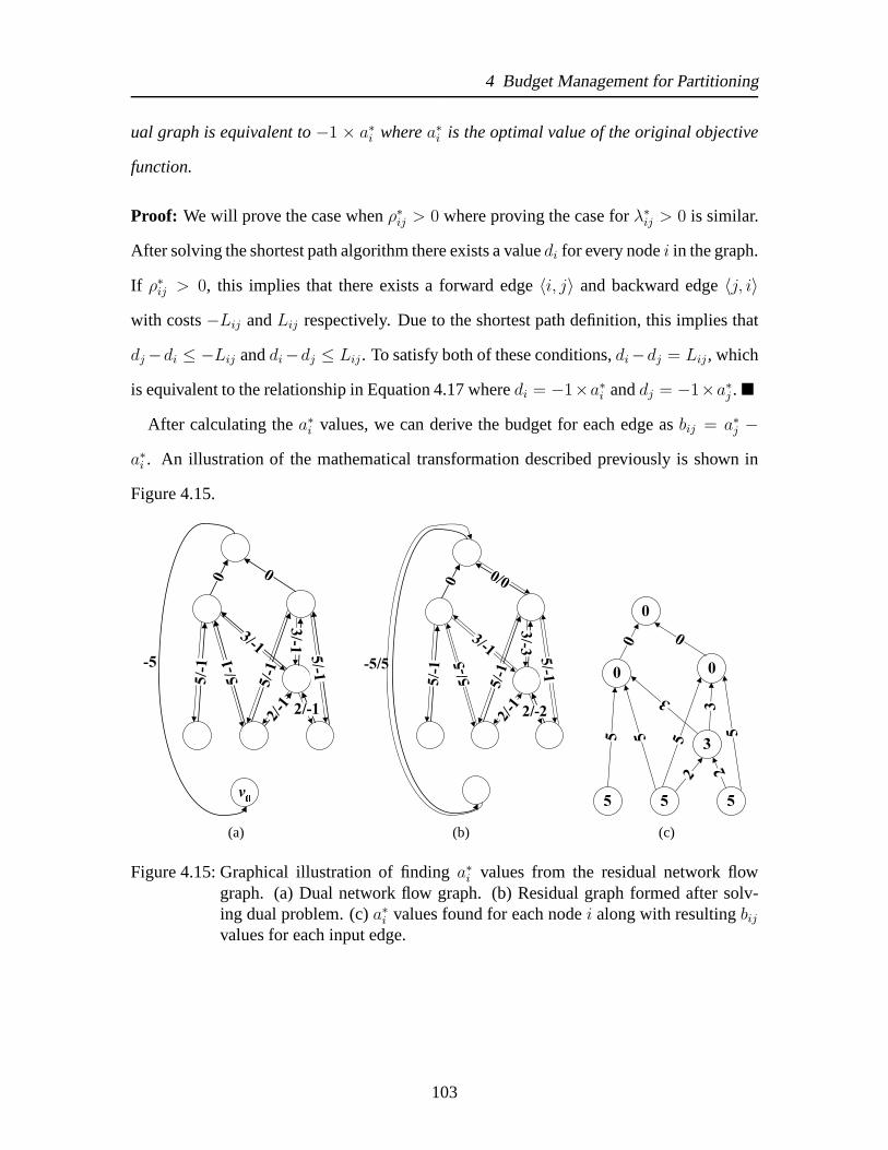
4 Budget Management for Partitioning
ual graph is equivalent to−1 × a∗i wherea∗
i is the optimal value of the original objective
function.
Proof: We will prove the case whenρ∗ij > 0 where proving the case forλ∗
ij > 0 is similar.
After solving the shortest path algorithm there exists a valuedi for every nodei in the graph.
If ρ∗ij > 0, this implies that there exists a forward edge〈i, j〉 and backward edge〈j, i〉
with costs−Lij andLij respectively. Due to the shortest path definition, this implies that
dj−di ≤ −Lij anddi−dj ≤ Lij . To satisfy both of these conditions,di−dj = Lij , which
is equivalent to the relationship in Equation 4.17 wheredi = −1×a∗i anddj = −1×a∗
j . �
After calculating thea∗i values, we can derive the budget for each edge asbij = a∗
j −
a∗i . An illustration of the mathematical transformation described previously is shown in
Figure 4.15.
5/-1
v�
5/- 15 /-1
3/-1 5/ -1
3/-1
2 / -1
-5
2/-1
0 0
(a)
5/-5
5/- 15 /-1
0 0/0
3/-3 5/ -1
3/-1
2 / -1
-5/5
2/-2
(b)
55
0 0
3
5 5 5
23
55
3
2
00 0
(c)
Figure 4.15: Graphical illustration of findinga∗i values from the residual network flow
graph. (a) Dual network flow graph. (b) Residual graph formedafter solv-ing dual problem. (c)a∗
i values found for each nodei along with resultingbij
values for each input edge.
103

4 Budget Management for Partitioning
Modelling area-delay relationship
In the previous sections, we introduced the area-delay relationship used for each partition
as a piecewise-linear convex function. This allows us to change the delay-area relationship
with respect to the delay, which often occurs when varying the depth of a given input path.
For example, in Figure 4.16, reducing the depth of inputa by 1 has no impact on area;
however, reducing the depth of inputa by 2 has an area penalty of 2 extra gates.
�(a)
(b)
�(c)
Figure 4.16: Illustration of area penalty with depth reduction and inverted edges.
To model the delay-area relationship, we leverage the information provided by the AIG,
where we count the number inverted edges along the longest path between the input and
the partition output. The key insight is that for a given input path, the depth of the path
can be reduced with no area penalty until the depth is reducedbeyond an inverted edge
along the path. This phenomenon is shown in the previous example in Figure 4.16 where
inputa caused an area penalty only when its path depth was reduced bymore than 1. Thus,
to reduce the depth of a path toMij , has no area penalty. However, modelling the delay-
area relationship as a constant does not model the fact that increasing the depth of an input
gives more slack to other paths, which in turn may be optimized for area. For example,
104

4 Budget Management for Partitioning
Figure 4.17 illustrates two partitions. If the path depth along inputa of the top partition is
reduced, this forces the path depth of inputb in increase as shown in Figure 4.17(b). This
could be harmful since the bottom partition may now need to reduce its depth since input
pathb is now longer, which in turn could lead to an area increase.
� �(a)
��(b)
Figure 4.17: Illustration of how reducing the depth of a pathimpacts decisions along otherpaths and partitions.
To take into account the issue highlighted in the Figure 4.17, we model the area-delay
relationship ofFij(bij) in the intervalbij ∈ [Mij , Uij] as a line with a slope of -1. Here,Uij
is an upper bound assigned tobij , which basically states that pathij cannot expand beyond
the depthUij . For the intervalbij ∈ [Lij , Mij ], Fij(bij) is modelled as a line with a slope of
-2. This states that attempting to reduce the depth of the partition input beyond the number
of inverted edges along the longest path has a stronger penalty. Here,Lij is a lower bound
assignment tobij which states that the depth of the input pathij cannot be reduced beyond
Lij .
105

4 Budget Management for Partitioning
0
2
4
6
8
10
12
14
L M U
b ij
F( b
ijij
)
Figure 4.18: Illustration of area-depth relationship for functionF (bij).
Assigning Upper and Lower Bound
For eachbij variable, we have an upper and lower boundUij andLij . To assign the upper
bound, we use the work presented in [BD97]. Here, the authorsdevelop a disjoint de-
composition algorithm based on the BDD data structure. Using a BDD representation of a
function, [BD97] shows how to decompose a BDD directly into basic gates and multiplex-
ers. The authors show how to efficiently find a decomposition that minimizes area using
the BDD data structure where most of the time a 2-input basic gate could be derived from
each node in the BDD. Knowing that the maximum depth of a givenBDD is N whereN
is the number of variables in the BDD and drawing from the workin [BD97] which shows
how we can map a BDD node directly to a 2-input gate in the majority of cases, we set the
upper bound for each edge toN . To set the lower bound, we take a look at two conditions.
If there are no inverted edges along a input to the root node ofthe partition, the path must
go through at least one AND gate, implying that the lower bound is 1. If there are inverted
edges along this path, it must go through at least one additional inverted edge, thus in this
106

4 Budget Management for Partitioning
case we set the lower bound to 2.
4.2.3 Resynthesis with Delay Budgets
Once we have a delay budget assigned to each incoming edge of apartition, we can resyn-
thesize the partition. To guide the resynthesis process, the delay budgets are used to alter
the input depth of each partition input. Doing so penalizes input paths which should be
optimized for depth, while giving freedom to input paths that can be optimized for area.
We alter the depth of each partition input, such that nodes with a small delay budget are
assigned a higher depth value. The depth assignment,δij , for a partitioni is defined as the
maximum budget assigned to its partition inputs minus the budget assigned to edge〈i, j〉
(Equation 4.18).
δij = Max{bij | j ∈ fanin(i)} − bij (4.18)
An example of this assignment is shown in Figure 4.19. In Figure 4.19(a), each number
assigned to the inputs represents the depth budget found after solving the dual problem
described previously. After this, we derive depth assignments,δij , for each inputj, where
in this caseMax{bij | j ∈ fanin(i)} equals 5. Looking at the depth assignments in
Figure 4.19(b), the inputs with an assignment greater than zero are penalized to alter the
input depth. This alters resynthesis decisions to attempt to reduce the path along penalized
input paths more than the depth along non-penalized input paths.
4.3 Results
We empirically validate our analysis in the previous sections here. First, we do a com-
parison between solving the budget management problem as anILP versus using the dual
problem that was derived in Section 4.2.2 . When solving budget management as an ILP,
we use the commercial MOSEK ILP solver [MOS08]. For the dual problem, we create our
107

4 Budget Management for Partitioning
abcde f3 34 554
(a)
abcde f2 21 001
(b)
Figure 4.19: Depth assignments to inputs after delay budgetassignments. (a) Delay bud-gets assigned to each partition input. (b) Depth adjustmentfound from Equa-tion 4.18. Assignments to each partition input are used to drive the resynthesisengine.
dual solver with the assistance of Andrew Goldberg’s network flow solver [Gol97]. Fol-
lowing this, we evaluate our budget management framework inthe context of a partition
based logic synthesis flow.
4.3.1 Dual Problem Performance
Table 4.2 illustrates our performance results between the commercial ILP solver and our
dual formulation where on average, the dual problem is two orders of magnitude faster than
solving the budget management problem in its native ILP form. Since we use the notion
of duality to achieve this speedup, optimality is preservedand the same result is found in
both the ILP formulation and dual problem. We ran our problemon over 100 different
IWLS circuits, where we show only the largest circuits in detail. In Table 4.2, the first
column lists the circuit name, followed by its size in terms of 2-input AND gates. The last
two columns lists the runtime in seconds of the MOSEK ILP solver followed by the dual
problem runtime using Goldberg’s network flow solver. The speedup experienced by the
dual solver is a necessary condition in order to apply our budget management problem in
108

4 Budget Management for Partitioning
Circuit nNodes TimeILP (sec) TimeNF (sec)b14_1 7196 27.72 0.40b14 8248 105.31 0.32
b15_1 12874 91.52 1.18b15 14008 60.56 1.66
b20_1 14124 128.11 0.96b21_1 14672 128.14 1.23b20 16452 154.31 1.02b21 17560 158.61 1.50
b22_1 21764 107.14 1.58b22 25144 217.34 2.06
b17_1 36692 1185.28 6.16b17 39956 3185.96 6.96
des_perf 88586 3185.96 6.96vga_lcd 152594 8530.26 17.27
ILP/NFave 101x
Table 4.2: Runtime comparison of ILP and NF formulation, over 100 circuits ran, onlylargest circuits shown. Run on a Pentium 4, 2.80GHz with 2GB of RAM
the context of logic synthesis.
4.3.2 Budget Management for Partitioned Logic Synthesis
After verifying that our dual formulation is indeed scalable to large designs, we applied our
budget management framework to logic synthesis. We compared two flows: a partitioned
based flow without budget management, and a partitioned flow with budget management.
To synthesize and technology map each partition, we used theABC logic synthesis engine
running the scriptresyn2.rc . After applying each logic synthesis flow, we measured
the area and depth of the resulting circuits in terms of 4-input LUTs.
Table 4.3 highlights our results when applied to the IWLS benchmark set (only larger
circuits shown in detail). In Table 4.3, the first column lists the circuit name, the next two
columns show the area results, and the final two columns show the depth results. For the
area results, we record the number of 4-input LUTs and show two columns of data listing
109

4 Budget Management for Partitioning
Area (4-LUTs) DepthCircuit NoBudget Budget NoBudget Budgetb14_1 1799 1791 21 19b14 2062 2068 22 20
b15_1 3005 3112 18 16b15 3189 3360 25 23
b20_1 3531 3546 26 22b21_1 3668 3670 26 21b20 4113 4135 27 23b21 4390 4359 27 23
b22_1 5441 5441 26 22b22 6286 6278 26 23
b17_1 9173 9181 18 16b17 9989 10230 38 32
des_perf 31977 31759 6 6vg_lcd 33165 34739 8 8
Ratio GeomeanALL 1.00 0.95Ratio GeomeanLARGE 1.01 0.89
Table 4.3: Impact of budget management framework on area anddepth for the IWLS set,only larger circuits shown in detail.
the non-budgeted results followed by the budgeted results.Similarly, the depth results
record the number of logic levels and show two columns listing the non-budgeted results
followed by the budgeted results. The second last line in Table 4.3 shows the average
comparison of the entire benchmark set. This shows that budgeting overall only improves
the circuit depth by 5%. However, after examining many circuits, it turned out that if a
partition could capture most of the critical paths in the circuit, budgeting was not necessary.
Budgeting is not necessary in such cases since a single partition has the true critical path of
the entire circuit does not need external information to optimally reduce the critical path of
the circuit. This phenomenon generally occurred in small circuits with a very low number
of logic levels. Ignoring these circuits, our improvement to circuit depth increases to 11%
with little impact to the final area. The improvements we achieve in Table 4.3 almost comes
for free as the overhead to run the budget management flow is negligible where it takes less
110

4 Budget Management for Partitioning
than 2 minutes for the larger IWLS circuits.
4.4 Summary
We have described a budget management framework which is empirically shown to be
scalable and applicable to improve a partitioned based logic synthesis flow. By converting
our budget management problem to its dual form, we show how wecan improve the runtime
of the application by two orders of magnitude. Furthermore,when applied in the context of
a logic synthesis flow, we improve the logic depth by 11% with negligible impact to area.
As partitioning becomes more common in existing CAD flows, budget management is
a necessary condition to ensure that QoR is maintained whileimproving the scalability of
the FPGA CAD flow.
111

5 Automation of ECOs
As FPGA design complexity increases, achieving tight timing and area constraints is be-
coming very challenging and often requires several design iterations as shown at the top of
Figure 5.1. Here, a design described in a Hardware Description Language (HDL) is passed
to an FPGA CAD flow such as Quartus II. If design constraints are not met after the CAD
flow finishes, the designer must modify their existing HDL code and rerun the CAD flow.
To complicate things, even if performance constraints are met, bug fixes or feature changes
may still be required. Applying these changes directly at the HDL and using a “from
scratch” FPGA recompile is often not an option since this does not guarantee that circuit
performance will be maintained. To avoid this problem, designers typically handle late-
stage changes through a process known as engineering changeorders (ECOs). ECOs are
small functional changes applied directly to a place-and-routed netlist such as the rewiring
of LUTs or changing LUT implementations. As a result, ECOs have a very predictable
impact on the final performance of the circuit and preserve much of the engineering effort
previously invested in the design.
In a design flow where almost all tasks are automated, ECOs remain a primarily manual
process. As a result, applying ECOs is very error-prone and can require several iterations
to correctly modify a design. This makes FPGA very difficult to use as a digital design
medium. The ECO process is illustrated in Figure 5.1 throughthe path labelled asOriginal
Flow. The feedback process shown inOriginal Flow can often tie up a designer for several
months [Mor06a, Gol04, Goe07, Pla05] which leads to missed project deadlines. To make
112

5 Automation of ECOs
things worse, this methodology will not scale since FPGA designs double in size with each
generation. With very short design cycles demanded today, this will be very detrimental to
a product’s success.
module foo (…)always @ (…)begin
…end…… ������������������ ��
�����! � �� ��! "�#�$%$%&'( &'($%&'()���*�#+����#�+,���*�-.��� $��!*/�#0�+,
)�# ��'*%+1 ��'*%+
��++2���3������#,4567689: ;:<=
>?= ;:<=Figure 5.1: Generalized flow using ECOs.
To avoid the expensive and error-prone nature of ECOs, we introduce a resynthesis ap-
proach that is able to automatically update the behaviour ofa circuit by using existing logic
within the design. This is beneficial since it requires no manual intervention. This can
potentially reduce the time spent on ECOs from weeks to a few hours.
The proposed flow is shown at the bottom of Figure 5.1 labelledasNew Flow. Unlike
theOriginal Flow, theNew Flowdoes not require an iterative approach. DuringNew Flow,
the circuit behaviour is updated using two steps. First, theproposed algorithm applies a
localization step which isolates nodes within the netlist which need to be changed. For
example, during bug-fixes, the localization step will isolate nodes which are the source of
113

5 Automation of ECOs
the erroneous behaviour of the circuit. Following this, theproposed algorithm applies a
resynthesis step to alter the circuit. The resynthesis stepfirst defines the function that will
replace the existing nodes found in the localization step. Next, the proposed algorithm
uses a SAT-based decomposition to break our necessary changes into a set of subfunctions.
During decomposition, subfunctions must exist within the place-and-routed netlist. This
ensures that the proposed algorithm has a predictable impact on the final performance of
the circuit. By using a SAT-based approach, we will show thatunlike previous approaches,
we can handle multiple changes and do not require a formal verification step to ensure that
our modifications are correct.
The ultimate goal of this work is to create an ECO flow which canautomatically update
the behaviour of a circuit in a manner which preserves as muchas possible the placement
and routing of the circuit while maintaining timing. This can be achieved by satisfying the
following three criteria:
• be minimally disruptive to an existing place-and-routed circuit.
• have little or no impact to the performance of a circuit.
• be robust enough to handle a wide range of changes.
In later sections, we will show that our approach does indeedsatisfy the previous three cri-
teria. In particular, when applied to Altera’s Stratix architecture using several benchmarks
from the Altera QUIP [Alt08] and the ITC benchmark suites we will show our technique
on average leaves over 90% of a place-and-routed circuit unchanged; has a marginal impact
to circuit performance where we reduce the frequency by lessthan 3% on average; and is
robust enough to handle over 80% of the changes presented. Inall cases, we require no
manual intervention by the user.
The rest of the chapter is organized as follows: Section 5.1 discusses the background
and related work; Section 5.2 describes the proposed algorithm in detail; Section 5.3 shows
114

5 Automation of ECOs
experimental results; and Section 5.4 concludes the chapter.
5.1 Background and Related Work
5.1.1 Terminology
The combinational portion of a LUT network can be represented as a directed acyclic graph
(DAG). A node in the graph represents a LUT, primary input (PI), or primary output (PO).
An edgein the graph with headv, and tailu, represents a signal in the logic circuit that is
an output of nodeu and an input of nodev. Primary inputs (PIs) are nodes with no inputs,
and primary outputs (POs) are nodes with no outputs.
A nodeu is atransitive fanout(fanin) of v if there exists a path between an input (output)
of u and an output (input) ofv. In this chapter, we will often use the term transitive fanout
or transitive fanin of a nodev to refer to all nodes which are a transitive fanout or transitive
fanin to nodev.
When defining a function at a nodev, it is termed aglobal functionif the function support
set consist of only PIs. Conversely, alocal functionis a function whose support set consists
of variables which may not be PIs. Asupport setof a function is the set of variables
that directly determine the output value of a function and the size of the support set is the
number of variables in the set.
5.1.2 Related Work
ECOs covers a wide range of work which is either used to incrementally improve the per-
formance of a design [CS00] or help modify the behaviour of a design such that circuit
performance is maintained [MCB89, CMB08, YSVB07, HCC99, Men05, Xil08]. Our
115

5 Automation of ECOs
work falls in the latter category where we focus on late-stage ECOs which are applied
directly to a place-and-routed netlist. Late-stage functional changes often occur due to
last minute feature changes or due to bugs which have been missed in previous verifi-
cation phases. The most recent steps toward the automation of the ECO experience in-
clude [CMB08] and [YSVB07]. Here, using formal methods and random simulation, the
authors in [CMB08, YSVB07] show how netlist modifications can be automated. To apply
modifications, the authors use random simulation vectors tostimulate the circuit. Using
the resulting vectors at each circuit node, they are able to find suggested alterations to their
design to match a specified behaviour. Following their modifications, they require a formal
verification step to ensure that their modification is correct. The results of their work is
promising where they can automatically apply ECOs in more than 70% of the cases they
present.
The technique in [YSVB07, CMB08] requires an explicit representation of any modifi-
cation, which does not scale to large changes. This is not a problem in ASICs since ECOs
requiring major changes are not desired since they are difficult to implement; however
in FPGAs, where we can reprogram logic cells without disrupting the placement, large
changes can be implemented while maintaining circuit performance. Our approach im-
proves on this where we can handle much larger changes by using a SAT-based approach
shown in the following sections.
5.1.3 Boolean Satisfiability (SAT)
For completeness, this section gives a brief overview of theSAT problem. A more detailed
description of the SAT problem is found in Chapter 2, Section2.5. Given a Boolean expres-
sionF (x1, x2, ..., xn), Boolean satisfiability (SAT) seeks an assignment to the variables,x1,
x2, ...,xn, such thatF evaluates to true. If this is possible,F is said to besatisfiable, oth-
erwise, it isunsatisfiable. SAT solvers are tools that serve to find if a Boolean formula is
116

5 Automation of ECOs
satisfiable or not. For practical reasons, modern day SAT solvers work on Boolean expres-
sions in Conjunctive Normal Form (CNF). An example of a Boolean expression is shown
in equationFAND in Figure 5.2
Recent advancement in SAT solvers [MMZ+01] have improved their runtime perfor-
mance by an order of magnitude, thus several problems in EDA can be practically solved
using SAT. In order to solve circuit problems with SAT, oftenthe circuit needs to be con-
verted into a Boolean expression which is then input into theSAT solver. This Boolean
expression [Lar92] is known as acharacteristic functionfor the circuit. The characteris-
tic function of a circuit evaluates to true if all variable assignments of the wires, inputs,
and outputs of the circuit have a feasible assignment. For example, consider theANDgate
shown in Figure 5.2. The table to the left gives the truth table for theANDgate character-
istic function which can be converted to CNF using any standard minimization technique.
Figure 5.3 shows how to derive the characteristic function of larger circuits by conjoining
the characteristic functions of individual gates within the circuit.
AZ
B
A B Z FAND
0 0 0 10 0 1 00 1 0 10 1 1 01 0 0 11 0 1 01 1 0 01 1 1 1
FAND = (A + Z)︸ ︷︷ ︸
· (B + Z) · (A + B︸︷︷︸
+Z)
clause literal
Figure 5.2: Characteristic function derivation for 2-input AND gate.
After deriving the characteristic function of a circuit, wecan use it in conjunction with
SAT solvers to examine logical properties of the circuit forvarious CAD problems. For
example, in Section 5.2.1, we will show a SAT-based technique using the characteristic
117

5 Automation of ECOs
YC
BZ
A
F =(A + Z) · (B + Z) · (A + B + Z) ·
(Z + Y ) · (C + Y ) · (Z + C + Y )
Figure 5.3: Cascaded gate characteristic function: top clauses fromANDgate; bottomclauses fromORgate.
function to isolate errors within a design.
In this chapter, we will often refer to a circuit as beingsatisfiablewithout explicitly
showing its characteristic function. We define a circuit as being satisfiable if there is a
satisfying assignment to the characteristic function of the circuit. The circuit is unsatisfi-
able if no such assignment exists. Furthermore, asatisfying assignmentto a circuit is an
assignment which is consistent with the circuit’s characteristic function. For example, one
possible satisfying assignment to the circuit in Figure 5.3is ABCZY = 01101.
5.2 Automated ECOs: General Technique
From a manual perspective, ECOs are applied by first isolating the logic that needs to be
changed. Following this, the designer must determine what to map the existing logic to,
that is, what new logic functions are required to correctly change the circuit. Finally, the
designer must determine how to implement these new logic functions within the context
of the existing place-and-routed circuit. In this work, we propose a method to automate
all of these steps using Boolean satisfiability. We do so by breaking our problem up into
two steps: netlist localization, followed by netlist modification. This flow is highlighted in
Figure 5.4.
Before netlist localization or netlist modification can occur, the desired behaviour of the
118

5 Automation of ECOs
Netlist Localization
MAX-SAT
based
Netlist Modification
Derive
Suitable Global
Function Fc
SAT-based
Derivation
Fc=h(g
1,g
2,…,g
k)
More
Focal Points
?
Changes to
Place & Routed
Netlist
NO
YES
Focal Points
Figure 5.4: Automated ECO flow: a MAX-SAT based netlist localization step followed bya SAT based Netlist Modification step.
circuit must be well defined. This is the behaviour that we ultimately want our circuit to
implement. To model this desired behaviour, we will use amodel netlist. This model netlist
is a logic netlist which defines the new input and output behaviour of the circuit. Once we
have the model netlist, netlist localization and modification can occur.
Netlist localizationfinds a set of locations which we will refer to asfocal points. These
focal points help isolate regions that need to be modified. Inthis work, we propose using
a MAX-SAT formulation first introduced in [SMV+07] to find our focal points. Following
netlist localization, thenetlist modificationoccurs. During this step, the proposed algo-
rithm will leverage existing logic found in the design to help rewire the nodes at each
focal point such that the resulting circuit will match the behaviour of the model netlist.
This starts by first deriving the proper global functionFc to replace the logic at each focal
point. After a new global function is found, a search of the netlist is conducted to find a
proper set of subfunctions,{g1, g2, ..., gk}, to implement the new global functionFc such
119

5 Automation of ECOs
thatFc = h(g1, g2, ..., gk). Since these subfunctions, which we will refer to asbasis func-
tions, already exist in the place-and-routed netlist, the only required changes to the netlist
revolves around the implementation of thedependency functionh. As we will show in
Section 5.2.2, implementingh requires much fewer changes than implementingFc from
scratch and in this work, we will show how we both select our basis functionsgi and derive
the dependency functionh using SAT. This makes the proposed algorithm well suited for
ECOs which must preserve the existing place-and-routed circuit as much as possible.
5.2.1 Netlist Localization
Netlist localization is the process of identifying which nodes must be changed in order to
change the behaviour of the circuit such that it matches the behaviour of the model netlist.
The approach we use to find these nodes is based upon the work presented in [SMV+07].
Here the authors introduce a localization technique based upon Maximum Boolean Satisfiability
(MAX-SAT). Like SAT, MAX-SAT seeks a satisfiable variable assignment to a CNF. How-
ever, in the case of unsatisfiability, MAX-SAT seeks an assignment which maximizes the
number of satisfying clauses. Using the set of unsatisfiableclauses, we can isolate discrep-
ancies between two netlists. @A BC D@A BC DEF F FEF F EFigure 5.5: Maximum satisfiability solution to localization.
This process is illustrated in the Figure 5.5. Consider the two circuits in Figure 5.5. The
top circuit is the model netlist while the bottom circuit is the implementation of the original
circuit. Under the input stimulus{a = 0, b = 1, d = 1} the original circuit has a response
of {e = 0} which conflicts with the model response of{e = 1}. The corresponding CNF
120

5 Automation of ECOs
for the original circuit and the input/output vectors are shown below.
(a) · (b) · (d) · (e) ·
(a + c) · (b + c) · (a + b + c) ·
(c + e) · (d + e) · (c + d + e)
(5.1)
The above equation is unsatisfiable; however, the MAX-SAT problem will attempt to
maximize the number of satisfied clauses. One possible solution to this is satisfying all
clauses except for clause(a + c). Since clause(a + c) is derived from theAND-gate, this
indicates that the function output from this gate (i.e. function on wire c) is the source
of the discrepancy. Clause(a) could have also been identified in the MAX-SAT solution
which does not help identify the discrepancy in our circuit.To avoid fruitless clauses from
being identified, such clauses can be forced a satisfying assignment prior to solving the
MAX-SAT problem.
This type of localization is known as trace-based localization where a vector set is used
to help identify discrepancies between two netlists. The main limitation with this approach
is that if only a small set of vectors or traces are available,false locations will be identified.
However, assuming that a large enough set of vectors are available, an iterative approach
can be applied to the localization process where the number of potential locations are re-
duced.
In our case, we will often refer to discrepancy points isolated by the localization point
asfocal points. Also, in many examples, we will assume there only exists onefocal point,
which we will refer to assingle-location modifications.
In the example shown in Figure 5.5, the original circuit and model netlist exist as a gate-
level netlist. This is not necessary, since we are only interested in the characteristic function
of the current circuit and IO response of the model netlist; not their implementation. This
is important in our case where our circuit exists as a netlistof LUTs on Altera’s Stratix
121

5 Automation of ECOs
architecture and our model netlist consists of a netlist of AND and inverter gates (AIG)
synthesized from an RTL netlist.
5.2.2 Netlist Modification
After netlist localization occurs, the netlist can be modified. Modifications are centered
around thefocal pointsthat were identified during the localization phase. Referring back
to Figure 5.4, the process of netlist modification requires aseries of steps. First, we must
define a global functionFc to replace the existing global function at each focal point.Fol-
lowing this, we must decompose the replacement functionFc such that it leverages existing
logic within the place-and-routed netlist. We will show later on that we use a special-
ized circuit construct to define an implicit representationof the on and offset ofFc. This
significantly enhances the scalability of our approach. Once we have found a suitable rep-
resentation forFc, we will then decomposeFc into a set of basis functions. Since our basis
functions already exist within the place-and-routed netlist, we have significant control in
how we decompose our function, which is a requirement if we want to minimally disrupt
the existing place-and-routed circuit.
To understand why we need to find a suitable global function toreplace the function at
each focal point, consider the circuit illustrated in Figure 5.6. Assume nodeξ is identified
during the localization step. The transitive fanin and fanout for nodeξ are labelled asTFI
andTFO . The inputs to the circuit are labeled as the variable setX, and the outputs of
the circuit are labeled as the variable setY. Also, note that we illustrate some of the input
branches to the transitive fanout with dotted lines which will be important later on in the
following figure (Figure 5.7). Assuming we can change the global functionH(Xp) to any
arbitrary functionFc(Xs) whereXp ⊆ X andXs ⊆ X, we can alter the circuit behaviour to
match our model netlist. Thus, the ECO problem becomes one offinding a suitable global
functionFc(Xs) to replace the existingH(Xp). This leads to the following definition and
122

5 Automation of ECOs
lemma.
Definition 5.2.1 Suitable Global Function: In the case of a single focal point, ξ, identified
during the localization step, a suitable global functionFc is defined as a function which can
be used to replace an existing global functionH found atξ such that the resulting circuit
matches the input-output behaviour of a model netlist.
Lemma 5.2.2 For a single-location modification, such as the one shown in Figure 5.6, the
circuit behaviour of the original circuit can be altered to match a model netlist if and only if
the global function located at focal pointξ is replaced with another suitable global function
Fc(Xs).
G
H)(ξTFO
ξ IJGKL)(ξTFIMNOPQRSTSUVWPQSQ XYQVZMNOPQRSTSUVWPQY[T XYQVZ
Figure 5.6: Illustration of localized nodeξ. Modification can be applied by replacingH(Xp) with some arbitrary functionFc(Xs).
Our work follows Lemma 5.2.2 where given a set of focal pointsreturned by the local-
ization step, we attempt to replace the global function at each location with another global
function. This requires us to first find a suitable global function, which we label asFc.
We do so by deriving an implicit representation ofFc using a specialized circuit construct.
123

5 Automation of ECOs
Following this, we search for a set of basis functions{g1,g2,...,gk} from the existing netlist
and see if they can be used to implement the new functionFc. This requires a SAT-based
functional dependency check described later on in this section. If the basis functions pass
the SAT test, we can generate the decompositionFc = h(g1, g2, ..., gk) whereh is known as
the dependency function betweenFc and the basis functions{g1,g2,...,gk}. To understand
this in detail, we will first consider the simple case of a combinational circuit containing a
single focal point returned from the localization step.
Deriving a suitable global function,Fc, can be done through brute force means where we
explicitly createFc. However, an explicit representation ofFc, such as a truth table or BDD,
will not scale sinceFc may depend on several variables. To avoid this problem we instead
choose to construct an implicit representation ofFc. We start off with a construction of the
circuit shown in Figure 5.7. On the left side of Figure 5.7(a)we show a circuit we intend to
modify, which looks similar to Figure 5.6. However, in Figure 5.7(a), we replace the focal
point ξ with an input pine. Doing so gives us the freedom to search for a suitableFc to
replace pine. Next, we have to constrain the input-output behaviour of the circuit to match
the model netlist. We do this by attaching the model netlist to our circuit as shown on the
left side of Figure 5.7(a). Here, we tie the circuit inputs together and connect the outputs
with anXORgate along with anORgate at the top. Following this, we force theORgate
output to 0 (q = 0). This equivalence construction is also known as a Miter circuit [Bry86]
and as a result of these constraints, any satisfying assignment to the circuit in Figure 5.7(a)
will be consistent with the input-output behaviour of the model netlist.
After constraining the circuit to the model netlist behaviour, we seek to remove the “don’t
care” space of the suitable functionFc. This gives us greater flexibility in choosing a proper
Fc. We do this by restricting the input space,X, to values where pine is observable at the
outputs. Informally,e, is observable at a PO,y, if for a given assignment, the value ofe
impacts the value ofy. Otherwise,e is not observable at nodey. This is appropriate since
124

5 Automation of ECOs
\
]^ _`abcdbecfgehij
(a) Attaching circuit to model netlist
k
lm nopqrsqtruvtwxyzx{
(b) Attaching observability constraints forCircuitConstrain
Figure 5.7: Circuit to be modified
125

5 Automation of ECOs
pin e will ultimately be replaced withFc. This is shown in Figure 5.7(b) which we will refer
to asCircuitConstrain. In CircuitConstrain, we duplicate the transitive fanout of pin
e. When connecting the duplicated transitive fanout to the original circuit, we complement
input pine, while all other input branches to the transitive fanout arekept the same. Also,
for each output pair of the duplicated transitive fanout andoriginal circuit, we add anXOR
gate followed by anORgate and set the output of theORgate to 1 (o = 1). The circuitry
added at the outputs along with the duplicated transitive fanout checks to see if the input
pin e is observable at the outputs. For example, if the output of theORgate is 0 (o=0), this
implies that the value on pine does not matter and will not affect the outputs. Based on the
previous description ofCircuitConstrain, we find the following lemma and proposition
to be true.
Lemma 5.2.3 CircuitConstrain is satisfiable if and only if the output of the current cir-
cuit matches the output of the model netlist and if pine is observable at the outputs.
Proposition 5.2.4 CircuitConstrain is satisfiable if and only if the assignment toe and
the assignment to the input vectorX is consistent with a suitableFc. In other words, for all
satisfying assignments toCircuitConstrain, Fc(X) = e.
Proof: Assume that if we have a satisfying assignment to
CircuitConstrain then the values one andX do not match any suitableFc. In other words,
assume that for a given satisfiable assignment toe andX thene 6= Fc(X). Thus, this im-
plies that the output of the current circuit does not match the model netlist by Lemma 5.2.2.
However, this is not possible since any satisfying assignment to CircuitConstrain must
match the input-output behaviour of the model netlist by Lemma 5.2.3. Thus, by contra-
diction any satisfying assignment toe andX implies a match to a suitableFc. Now let us
assume that if the values one andX match a suitableFc then we do not have a satisfying
assignment toCircuitConstrain. In this case, ife = Fc(X), then the output response of
126

5 Automation of ECOs
our circuit will match the model netlist. Also,e must be observable since we can restrict
the inputs space ofX to the observable space ofFc. However, these two conditions must
imply that we must have a satisfying assignment toCircuitConstrain by Lemma 5.2.3.
Thus, by contradiction, if the values one andX match a suitableFc then we have a satis-
fying assignment toCircuit-Constrain. Hence we have proved thatCircuitConstrain
is satisfiable if and only if the assignment toe and the assignment to the input vectorX is
consistent with a suitableFc. �
By proposition 5.2.4, we can use the circuit in Figure 5.7(b)to find a suitableFc by
exploring all satisfying assignments toe andX. Doing so will effectively create the entire
truth table for functionFc. For example, we would start by settingX to 000...00. We would
then find a satisfying value fore. This value found fore would representFc(000...00).
Next, we would continue forX = 000...01 and so on.
The problem with the previously described approach is that this requires an exhaustive
traversal of the input spaceX, which does not scale. Furthermore, implementingFc directly
is not desirable since this may require significant changes to the existing place-and-routed
netlist. A more practical approach for ECOs would be to search for a set of basis functions,
{g1, g2, ..., gk}, found from the existing netlist and check if this set of basis functions can
be used to implementFc such thatFc = h(g1, g2, ..., gk). Informally, this will be possible
if and only if there does not exist a situation where the output values of the basis functions
{g1, g2, ..., gk} are equivalent for a given pair of input vectors andFc is not equivalent for
the same pair of input vectors. For example, consider Figure5.8. Here we show four
functions,g1, g2, g3, andFc. In this example, all functions are dependent on three variables
x1, x2, andx3. Looking at functiong1 andg2, we see that there exists a given input pair
{000, 001} whereg1 andg2 are equivalent, butFc is not equivalent. Thus, it is impossible
to find a functionh such thatFc = h(g1, g2). In contrast, if we select functionsg1 andg3, it
is impossible to find an input pair whereg1 andg3 are equivalent andFc is not equivalent.
127

5 Automation of ECOs
Thus, in this case, there exists a dependency functionh such thatFc = h(g1, g3) (in this
caseh = g1 · g3 + g1 · g3). This process is beneficial since only the dependency function
h needs to be derived, which in general should have a smaller support set than the global
functionFc. This is ideal for ECOs since implementing the dependency functionh within
the existing circuit has a much smaller and predictable impact than implementing the entire
global functionFc from scratch.
x1x2x3 g1 g2 g3 Fc
000 0 0 0 1001 0 0 1 0010 0 0 0 1011 0 1 1 0100 0 0 1 0101 0 0 1 0110 1 0 1 1111 1 1 1 1
Figure 5.8: Functional dependency example
To formally check the condition described previously we will use a SAT-based ap-
proach [LJHM07]. This requires constructing a characteristic function that checks for
the following condition: for a given set of basis functions{g1, g2, ..., gk}, does there ex-
ist a minterm pair where the basis functions are equivalent and Fc is not equivalent. To
create this characteristic function, we construct the circuit shown in Figure 5.9. In Fig-
ure 5.9, we have duplicatedCircuit-Constrain and labeled them asCircuitConstrain0
andCircuitConstrain1. In each duplicated copy, we have simplifiedCircuitConstrain
and have only shown their duplicated input and output pins.
To check if there exists a minterm pair where a set of basis functions output values are
equivalent, we can extract a basis function set from each duplicated circuit and connect
them together with anXOR-ORgate network and set theORgate output to 0 (d = 0) as
shown in Figure 5.9. Here, we have selected two wiresg1 andg2 as the basis functions. The
128

5 Automation of ECOs
|}~}��
�}��
����}�����|�}����|�}�
| �~���
����
�������|������|�����������~�������} ��������~��������
Figure 5.9: Deriving global functionF = h(g1, g2) using dependency check construct.
support set of the basis functionsg1 andg2 in CircuitConstrain0 (CircuitConstrain1)
are labeled asXs0 (Xs1) which is a subset of the variable setX0 (X1). Due to these con-
straints, a satisfying assignment to Figure 5.9 will find an minterm pair assignment to vari-
ablesX0 andX1 where the basis functions are equivalent.
To check if there exists a minterm pair whereFc is not equivalent, we can also use the
circuit construct in Figure 5.9. Here, we will constrain each duplicated pine. Since in
CircuitConstrain, only satisfiable assignments toe andX are consistent with a suitable
global functionFc(X) by proposition 5.2.4, constraininge to 0 or 1 provides a means to
constrain the inputX to the offset and onset forFc(X). This is stated more formally in the
following lemma.
Lemma 5.2.5 In CircuitConstrain of Figure 5.7(b), if pine is assigned a value 0,
CircuitConstrain is satisfiable if and only if the input vectorX is assigned a value found
in the offset of the functionFc(X). Conversely, if pine is assigned a value 1, the circuit
is satisfiable if and only if the input vectorX is assigned a value found in the onset of the
functionFc(X).
Following from Lemma 5.2.5, the circuit in Figure 5.9 constrainse0 to 0 ande1 to 1 to
restrict the possible assignments toX0 andX1. Specifically, settinge0 to 0 constrains all
129

5 Automation of ECOs
possible assignments ofX0 to the offset ofFc, while settinge1 to 1 constrains all possible
assignments ofX1 to the onset ofFc. Thus, due to these constraints, a satisfying assignment
to Figure 5.9 will find a minterm pair assignment to variablesX0 andX1 that respectively
map to the offset and onset of functionFc. Thus, for this minterm pair,Fc is not equivalent.
Using the previous circuit constraints in Figure 5.9, we cancreate the characteristic func-
tion shown in Equation 5.2.
∃X0∃X1 (CircuitConstrain0 CNF ) ·
(CircuitConstrain1 CNF ) ·
(e0 ≡ 0) · (e1 ≡ 1) · (g1(Xs0) ≡ g1(Xs1)) ·
(g2(Xs0) ≡ g2(Xs1)) · (X0 6= X1)
(5.2)
In Equation 5.2, assume thatCircuitConstrain0 CNF (CircuitConstrain1 CNF ) repre-
sents the clauses derived from the characteristic functionof CircuitConstrain0 (CircuitConstrain1).
Equation 5.2 asks if there exists a minterm assignment pair to X0 andX1 which map to the
off and onset ofFc respectively (i.e.e0 ≡ 0 ande1 ≡ 1), while the basis functions are
equivalent. This leads to the following proposition.
Proposition 5.2.6 If Equation 5.2 is satisfiable the basis functions,gi, cannot be used to
implement a suitable global functionFc. If Equation 5.2 is unsatisfiable, the basis func-
tions,gi, can implement a suitable global functionFc.
Proof: Assume if Equation 5.2 is satisfiable thenFc has a decompositionh(g1, g2, ..., gk).
If Equation 5.2 is satisfiable, this implies that there is a vector assignmentC0 to X0 which
maps to the offset ofFc and there exists a vector assignmentC1 to X1 which maps to
the onset ofFc, which follows from Lemma 5.2.5. This also implies that vector C0 and
vectorC1 map to the same output vector,K = k1k2...kk in the output space of the basis
set{g1, g2, ..., gk} due to thegi equality constraints in Equation 5.2. However, since we
130

5 Automation of ECOs
have assumedFc = h(g1, g2, ..., gk) in the first statement, this impliesFc(C0) = h(K) = 0
andFc(C1) = h(K) = 1, thus we have a contradiction. Thus if Equation 5.2 is satisfiable
then Fc cannot be decomposed intoh(g1, g2, ..., gk). To prove the second statement in
proposition 5.2.6, we can use a similar argument and will notshow it in detail here.�
Equation 5.2 is a set of propositions which must be broken (i.e. Equation 5.2 must be
unsatisfiable) in order to identify a suitable set of basis functions. This process is equivalent
to property checking on a given circuit and is known to be NP-complete [CL73]. Also,
although intractable, heuristic SAT solvers have proven tobe able to find solutions to these
problems without needing to apply an exponentially number of operations with respect to
the problem size.
If Equation 5.2 is unsatisfiable, we can derive the correct dependency functionh from
the proof of unsatisfiability. This requires backtracing through the set of clauses that are
the source of the unsatisfiable condition and creating a function based on these clauses. In
our case, if the functionh is small enough (its support set size is less than 20), we create a
BDD representation ofh. We limit the variable size to 20 since this minimizes the risk of
BDD explosion [BS02]. In the cases where the BDD does get verylarge, we fail to create
a proper implementation ofh. Derivingh based on the proof of unsatisfiability is based on
the theorem of Craig interpolation and will not be discussedhere. For a detailed description
on derivingh please refer to [McM03] and [LJHM07].
If the support size ofh is less than the number of inputs to a LUT, we can implementh
in a single LUT and the modification process is complete. However, if the support size of
h is larger than the number of inputs to a LUT, we must decomposeand technology map
h to the circuit architecture. In our case, we decomposeh into a network of LUTs for the
Stratix architecture. However, one can modify their decomposition algorithm to maph into
any technology. During the decomposition, since timing information is available, we skew
the decomposition such that critical wires are placed near the top of the decomposition tree.
131
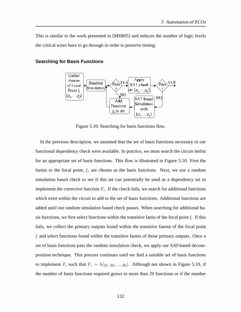
5 Automation of ECOs
This is similar to the work presented in [MSB05] and reduces the number of logic levels
the critical wires have to go through in order to preserve timing.
Searching for Basis Functions�������������� �� �¡¢���� £¤¥¦§ §̈¥© ª «��¬�®�¯¡����� °¬¬�¯� ����¥± �� ���°²²¡³®°´ �� µ�� ¤¥¦§ §̈¥¶ª ·¸ ¹º®·¸¹º®¢���» ¢���»®°´ ¼���¬®�¯¡�����½���¤¥¦§ §̈¥¶ª
Figure 5.10: Searching for basis functions flow.
In the previous description, we assumed that the set of basisfunctions necessary in our
functional dependency check were available. In practice, we must search the circuit netlist
for an appropriate set of basis functions. This flow is illustrated in Figure 5.10. First the
fanins to the focal point,ξ, are chosen as the basis functions. Next, we use a random
simulation based check to see if this set can potentially be used as a dependency set to
implement the corrective functionFc. If the check fails, we search for additional functions
which exist within the circuit to add to the set of basis functions. Additional functions are
added until our random simulation based check passes. When searching for additional ba-
sis functions, we first select functions within the transitive fanin of the focal pointξ. If this
fails, we collect the primary outputs found within the transitive fanout of the focal point
ξ and select functions found within the transitive fanins of those primary outputs. Once a
set of basis functions pass the random simulation check, we apply our SAT-based decom-
position technique. This process continues until we find a suitable set of basis functions
to implementFc such thatFc = h(g1, g2, ..., gk). Although not shown in Figure 5.10, if
the number of basis functions required grows to more than 20 functions or if the number
132

5 Automation of ECOs
random simulation calls is more than 10, the search will terminate.
x1x2x3 e g1 g2 g3
100 0 0 0 1001 0 0 0 1010 1 0 0 0011 0 0 1 1110 1 1 0 1101 0 0 0 1
Figure 5.11:Random simulation example.
The random simulation check shown in Figure 5.10 is used as a quick check to see if the
current basis function set can be used to implementFc without going through the more ex-
pensive SAT-based check described in the previous section.Here, using
CircuitConstrain in Figure 5.7(b), we randomly simulate the PIsX and pine. Vec-
tors which violate the observability (o = 1) and equality (q = 0) constraint are discarded.
Following this, we search through the circuit netlist and find a set of nodes whose vectors
do not satisfy Equation 5.2. For example, consider Figure 5.11. Assume that the circuit PIs
are variablesx1, x2, andx3 and functionsgi are chosen from the existing circuit. Here we
show the value of the functions,gi, with respect to a random input vector assignment to the
PIs and pine. Using this sample set, we can see that the set{g1, g2} cannot be used as our
basis set since there exists a primary input pair,{001, 010}, which satisfies Equation 5.2. In
contrast, basis set{g1, g3} is a possible set since there does not exist any input pair which
satisfies Equation 5.2. Since our random simulation set is not exhaustive, we must apply
the SAT-based check described in the previous section to cover any input vectors missed
during the random simulation.
If the current basis set fails the random simulation test, wemust add additional functions
to build a proper set of basis functions. To help guide the search, we use a SAT based
vector generation to create input patterns that can find additional vector pairs that need to
be differentiated. The SAT based vector generation works by duplicating the circuit and
133

5 Automation of ECOs
“locking” each pair of duplicated basis functions to equivalent values and setting the pair
of duplicated input pinse to complemented values. Following this, a SAT solver is run
32 times to find a set of 32 different satisfying values on the other wire which generates a
new vector set. Using these new vector sets, we search for functions that candifferentiate
minterms currently differentiated by pine, but not differentiated by the current basis func-
tion set. Informally, a function set candifferentiatea pair of minterms if their outputs are
different for that minterm pair. For example, in Figure 5.11, {g1, g2} cannot differentiate
minterms001 and010 sinceg1(001) ≡ g1(010) andg2(001) ≡ g2(010). Since pine differ-
entiates this pair, to create a valid basis set from{g1, g2} for pin e, we would need to pick
an additional functiongj that can differentiate vectors001 and010 (differentiating pairs
{100, 010} and/or{101, 010} are also possible). Wires whose functions cover the most
vectors not differentiated by the current basis set are chosen first. This greedy algorithm
helps to minimize the size of the basis function set. The second criteria when choosing
basis functions is their timing criticality: basis functions with non-critical wires are chosen
over basis functions with critical wires.
Partitioning of Circuit and Treatment of Registers
In order to help reduce the size of Equation 5.2, we can removeportions of the circuit
which do not impact the behaviour of the current node being modified. This is illustrated
in Figure 5.12. Here, we are assuming that nodeξ was localized in our netlist localiza-
tion step. Using nodeξ, we collect the set of outputs within the transitive fanout of ξ, as
shown in Figure 5.12(a). Following this, we collect the transitive fanin of each output, as
shown in Figure 5.12(b). Since the POs of the implemented netlist may require that their
transitive fanin PIs be changed during the modification, thetransitive fanin collected in
Figure 5.12(b) is defined by the model netlist. Thus, this requires that our model netlist
be a white-box implementation, such as an gate-level netlist derived from an RTL descrip-
134
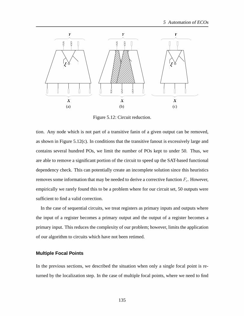
5 Automation of ECOs
¾
¿ξ
(a)
À
Áξ
(b)
Â
Ãξ
(c)
Figure 5.12: Circuit reduction.
tion. Any node which is not part of a transitive fanin of a given output can be removed,
as shown in Figure 5.12(c). In conditions that the transitive fanout is excessively large and
contains several hundred POs, we limit the number of POs keptto under 50. Thus, we
are able to remove a significant portion of the circuit to speed up the SAT-based functional
dependency check. This can potentially create an incomplete solution since this heuristics
removes some information that may be needed to derive a corrective functionFc. However,
empirically we rarely found this to be a problem where for ourcircuit set, 50 outputs were
sufficient to find a valid correction.
In the case of sequential circuits, we treat registers as primary inputs and outputs where
the input of a register becomes a primary output and the output of a register becomes a
primary input. This reduces the complexity of our problem; however, limits the application
of our algorithm to circuits which have not been retimed.
Multiple Focal Points
In the previous sections, we described the situation when only a single focal point is re-
turned by the localization step. In the case of multiple focal points, where we need to find
135

5 Automation of ECOs
multiple suitable global functions, we apply a step-by-step approach where we modify each
focal point one at a time. While modifying a given focal point, ξ, additional focal points
are “locked down” such that they are set to fixed values. For example, one overly simplistic
heuristic would be to set all focal points other thanξ to value 0 (in general, this would not
work since this could make the focal pointξ unobservable at the outputs, such as in a case
whereξ and another focal point enter into a singleANDgate). This ensures that changes
seen at the output are due to the focal pointξ, and not due to the other focal points found
within the netlist. The locking down of focal points has the possibility of not converging,
particularly for complex changes requiring several modifications. However, in practice the
step-by-step heuristic works in the majority of cases as shown empirically in Section 5.3
where we have at most four focal points into the design.
5.3 Results
To ensure that the resynthesis technique described in the previous sections can be applied to
late-stage ECOs, we must ensure that our technique can automatically update the behaviour
of a circuit while minimally disrupting the existing place-and-routed netlist and preserve
timing. Thus, we evaluate our work based on three criteria: how disruptive our technique
is on a place-and-routed netlist, how much impact our technique has on performance, and
how robust our technique is in handling changes. Two experiments will be run to quantify
these three criteria. The first experiment models a late-stage specification change at the
RTL, while the second experiment models a late-stage bug fix.We run our algorithm on
circuits from Altera’s QUIP [Alt08] and the ITC benchmark suite.
All experiments are run on a PentiumD 3.2 GHz processor with 2GB of RAM. Circuits
are synthesized using Quartus II 7.1 and for Altera’s Stratix architecture. To communicate
136
5 Automation of ECOs
with Quartus II, we use Altera’s QUIP TCL interface [Alt08].
5.3.1 Specification Changes
In our first set of experiments, we seek to see how disruptive our approach is on an existing
place-and-routed circuit and its impact on performance. This is important for late-stage
ECOs since we want to preserve as much as possible the engineering effort invested previ-
ously when applying our changes. During this experiment, weapply a late-stage specifica-
tion change both using a full recompile of the design and using the proposed ECO approach.
During the experiment, we first implement a circuit described in Verilog or VHDL using
Altera’s Quartus II CAD flow. In the initial compile, we use Altera’s design space explorer
to achieve the best possible timing performance. Next, we modify the original HDL code
and use this modified code as our new specification (this wouldbe themodel netlistas
described in Section 5.2). Modifications are primarily constrained to control-path code or
modifications tocase andif-else statements where we change less than three lines of
code. An example of such changes is shown in Figure 5.13. After our code is modified,
we perform a full recompile of the modified HDL code and recordthe performance impact.
For comparison, we also apply the required HDL changes directly to the optimized circuit
using our ECO approach and record its performance impact andmeasure the disruption to
the place-and-routed netlist.
To quantify the disruption to the existing netlist due to a full recompile and from the ECO
compile, we measure the percent change in timing and the percentage of LUTs and wires
disrupted in the original place-and-routed circuit. Theseresults are shown in Table 5.1. The
first column shows the circuit name,Circuit, followed by three major column groups. The
first group,Before, reports the circuit size in terms of LUTs and timing numbersduring the
initial compile of the design (i.e. before applying any changes). Timing numbers report
the minimum clock period in terms of nanoseconds. The next group of columns headed
137
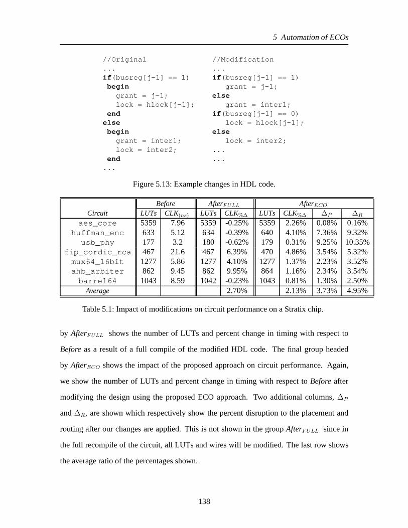
5 Automation of ECOs
//Original //Modification... ...if(busreg[j-1] == 1) if(busreg[j-1] == 1)begin grant = j-1;
grant = j-1; elselock = hlock[j-1]; grant = inter1;
end if(busreg[j-1] == 0)else lock = hlock[j-1];begin else
grant = inter1; lock = inter2;lock = inter2; ...
end ......
Figure 5.13: Example changes in HDL code.
Before AfterFULL AfterECO
Circuit LUTs CLK(ns) LUTs CLK%∆ LUTs CLK%∆ ∆P ∆R
aes_core 5359 7.96 5359 -0.25% 5359 2.26% 0.08% 0.16%huffman_enc 633 5.12 634 -0.39% 640 4.10% 7.36% 9.32%
usb_phy 177 3.2 180 -0.62% 179 0.31% 9.25% 10.35%fip_cordic_rca 467 21.6 467 6.39% 470 4.86% 3.54% 5.32%
mux64_16bit 1277 5.86 1277 4.10% 1277 1.37% 2.23% 3.52%ahb_arbiter 862 9.45 862 9.95% 864 1.16% 2.34% 3.54%
barrel64 1043 8.59 1042 -0.23% 1043 0.81% 1.30% 2.50%Average 2.70% 2.13% 3.73% 4.95%
Table 5.1: Impact of modifications on circuit performance ona Stratix chip.
by AfterFULL shows the number of LUTs and percent change in timing with respect to
Beforeas a result of a full compile of the modified HDL code. The final group headed
by AfterECO shows the impact of the proposed approach on circuit performance. Again,
we show the number of LUTs and percent change in timing with respect toBeforeafter
modifying the design using the proposed ECO approach. Two additional columns,∆P
and∆R, are shown which respectively show the percent disruption to the placement and
routing after our changes are applied. This is not shown in the groupAfterFULL since in
the full recompile of the circuit, all LUTs and wires will be modified. The last row shows
the average ratio of the percentages shown.
138

5 Automation of ECOs
As our results show, the results of a “from scratch” recompile shown in columnsAfterFULL,
are fairly acceptable on average where performance decreases by 2.70%. However, when
examining the individual performance impact of each circuit, we see that the results varies
by a large amount from -0.62% to 9.95%. This illustrates the unpredictable nature of a
full recompile on circuit performance. Furthermore, during a full recompile, the entire
netlist is disrupted, thus all of the placement and routing effort invested previously is lost.
In contrast, the proposed ECO approach has a much more predictable impact to perfor-
mance where the performance change varies between 0.31% to 4.86%. Also, the average
disruption of our approach is relatively low where we keep over 95% of the placement
and routing unchanged. Based on what is reported in industry[Mor06a], we feel that this
number is acceptable to most designers, which is a necessarycondition for the practical
use of our approach. In terms of runtime, the proposed ECO approach is approximately 2x
faster than performing a full compile. However, this discrepancy in runtime has more to
do with the internal algorithms of Quartus II than our work and thus, detailed numbers are
not shown. Furthermore, runtime comparisons would not reflect the reduction in time from
going from a manual process, which often takes several days,to the proposed automatic
ECO approach, which takes a few hours to complete.
During our experiments, we found that the class of changes weapplied did not create
drastic changes to the netlist. Specifically, during the localization process, all of our HDL
changes would result in less than five focal points being returned. In cases where five
or more focal points were returned, we found that our approach had difficulty finding a
non-disruptive modification to the place-and-routed netlist.
We should note that we used Quartus II’s TCL ECO interface to change and legalize the
circuit. Unfortunately, the TCL ECO interface does not provide an incremental placement
flow. Instead, Quartus II will apply a limited placement algorithm to new or modified
nodes. Here, the ECO placer will only move nodes to existing free locations within the
139

5 Automation of ECOs
FPGA and will not displace pre-existing nodes within the netlist. As a result, this may hurt
timing significantly since circuitous routes can be createdby new nodes. To overcome this
limitation, we manually unplace a small region surroundingeach new node. This gives
the placer much more flexibility in where to place nodes and reduces the impact of newly
introduced nodes. However, if given access to a full incremental placement algorithm, we
feel that our timing and disruptive impact would be less thanwhat is shown in Table 5.1.
5.3.2 Error Correction
In our second set of experiments, we apply the proposed ECO technique to fix errors in-
serted into a design. Errors include rewiring of LUTs or changing the LUT functions of
various nodes. To stress the approach, multiple errors are inserted into the design such that
the errors interact with each other. Errors interact when they are inserted at nodes whose
transitive fanouts overlap with each other. This is necessary to ensure that the complexity
of the correction increases as more errors are added to the design. After errors are in-
serted into the design, Quartus II’s place-and-route is rerun on the circuit to achieve the
best performance possible.
Table 5.2 shows our results for various circuits when five errors are inserted into the
design. The first columnCircuit lists the circuit name. This is followed by two column
groups:BeforeandAfterECO. Beforelists the number of LUTs and timing numbers before
the application of the ECO fix. Timing numbers report the minimum clock period in terms
of nanoseconds.AfterECO lists the total number of LUTs after the ECO fix and the rela-
tive change in timing with respect to the the timing reportedin theBeforecolumn. Also,
additional columns∆P and∆R are shown which respectively show the percent disruption
of the placement and wires after the ECO fix is applied. The final row shows the average
of the percentages. Unlike the previous results shown in Table 5.1, comparisons with a
full recompile is not done in this case since a designer wouldbe required to fix the error
140

5 Automation of ECOs
Before AfterECO
Circuit LUTs CLK(ns) LUTs CLK%∆ ∆P ∆R
aes_core 5359 7.95 5359 0.00% 1.12% 1.28%huffman_enc 633 5.08 633 0.20% 3.16% 3.61%
usb_phy 177 3.13 177 0.00% 13.56% 10.33%fip_cordic_rca 467 21.6 471 2.31% 12.85% 14.68%
mux64_16bit 1277 5.86 1277 0.51% 4.70% 5.37%ahb_arbiter 865 8.97 972 16.83% 6.94% 7.93%
barrel64 1041 8.58 1041 -4.66% 5.76% 6.59%b03 59 3.37 59 0.89% 16.95% 19.37%b04 184 6.56 184 -9.60% 32.61% 37.27%b08 58 3.68 58 5.71% 8.62% 9.85%b09 50 3.97 50 -3.02% 16.00% 11.43%b10 78 3.79 79 -17.41% 10.26% 11.72%b11 167 6.68 187 4.64% 9.58% 10.95%b12 378 6.17 381 3.40% 4.23% 4.84%b14 3014 8.17 3015 2.57% 1.99% 2.28%b15 6012 9.17 6023 6.98% 1.00% 1.14%
Average 0.18% 9.33% 9.91%
Table 5.2: Automated correction results on a Stratix chip.
manually by hand, which in many of the cases could not be practically solved by hand in
an efficient manner. The proposed technique, however, can find a fix automatically.
Table 5.2 shows that the proposed ECO technique has a marginal impact to timing where
we reduce timing on average by 0.18%. This is potentially misleading since for some
circuits, such asb04 andb10 , we improve timing by a large amount. This can occur in
some rare cases since the decomposition of the dependency functionh is timing driven and
has the potential to shorten the critical path. After removing these outliers, the average
impact to timing is 1.72%. Another outlier,ahb_arbiter , proved difficult to correct
where we found that in this circuit, the proper alterations required more than 15 basis
functions to correct it, which ultimately disrupted its timing significantly. Considering
that the proposed technique applies ECO changes in an automated fashion within minutes,
we feel that 1.72% is an acceptable tradeoff of timing for improved designer productivity
141

5 Automation of ECOs
where the designer would manually fix these problems in a spanof several days. Also,
we found that many of the fixes occurred on paths that were critical or near critical. Thus,
without a timing driven decomposition ofh and a timing driven search for basis functions,
circuit performance would not be maintained.
In terms of average disruption to the existing netlist, we disturb approximately 10% of
the place-and-routed netlist during our correction. We should note that this disruption is
skewed by the fact that for smaller circuits, a large relative disruption cannot be avoided.
For example, in the extreme case where a circuit contains only five LUTs, fixing five errors
in the circuit would disrupt 100% of the netlist. If circuitswith less than 200 LUTs are
removed from Table 5.2, the average disruption to the placement and routing drops to
approximately 5%.
When inserting less than five errors into the design, we foundwe were able to correct
over 80% of the circuits. However, as the number of errors increased, the circuit correction
problem became significantly difficult. This was primarily due to the localization step.
For complex fixes, the localization step often returns several focal points, which can be
much more numerous than the number of errors injected into the design. This significantly
complicates the correction process both in terms of deriving a suitable global functionFc
and minimizing the disruption to the existing netlist. Fortunately, the likelihood that large
errors are not detected early in the design flow is low and, as aresult, applying large changes
with late-stage ECOs is not a likely occurrence.
As a final experiment, we examined the impact of the the primary output removal heuris-
tic described in Section 5.2.2. This is shown in Figure 5.14 where we show the percentage
of outputs removed versus the runtime of the SAT solver when correcting circuitb15 . Dur-
ing this experiment, we inserted bugs into nodes whose transitive fanouts contained more
than 300 primary outputs and registers. Following this, we removed a percentage of outputs
or registers and attempted to rectify the circuit. After rectification, we recorded the runtime
142
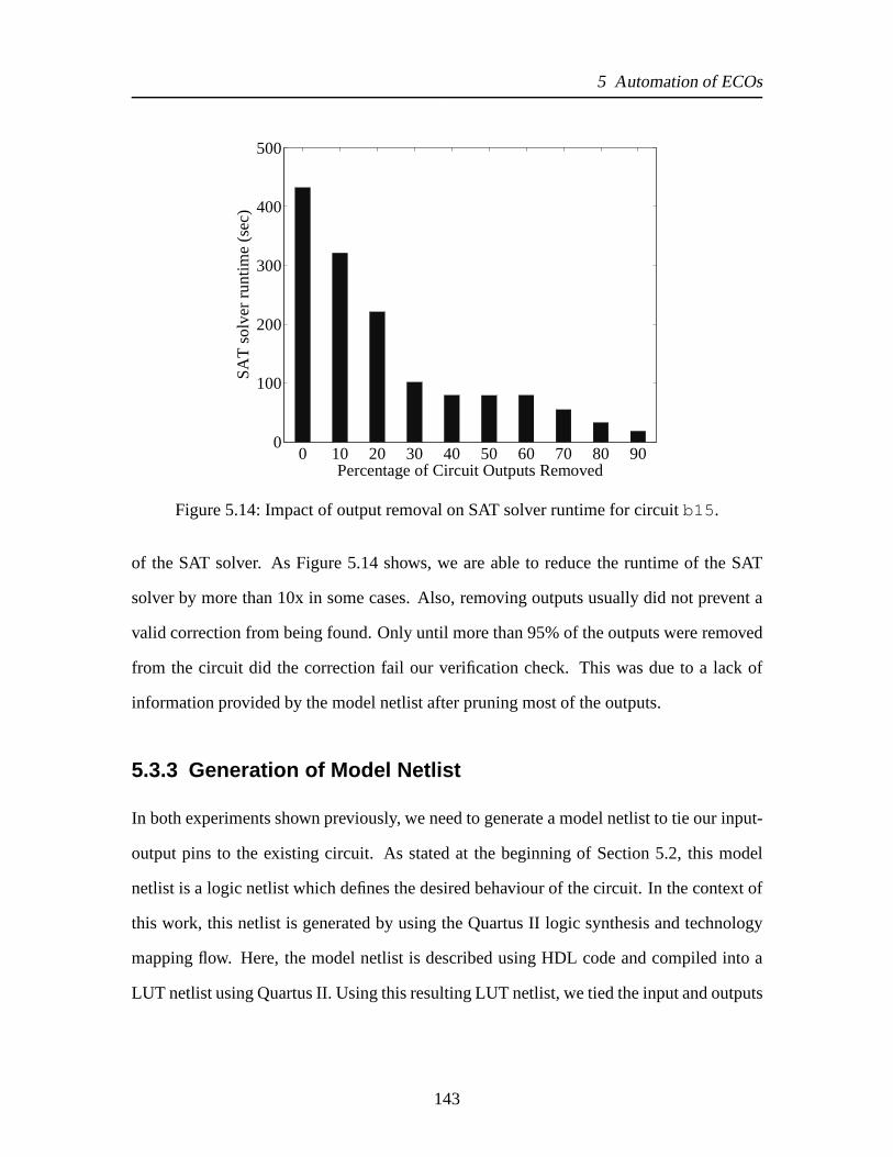
5 Automation of ECOs
0 10 20 30 40 50 60 70 80 900
100
200
300
400
500
Percentage of Circuit Outputs Removed
SA
T s
olv
er r
un
time
(sec
)
Figure 5.14: Impact of output removal on SAT solver runtime for circuitb15 .
of the SAT solver. As Figure 5.14 shows, we are able to reduce the runtime of the SAT
solver by more than 10x in some cases. Also, removing outputsusually did not prevent a
valid correction from being found. Only until more than 95% of the outputs were removed
from the circuit did the correction fail our verification check. This was due to a lack of
information provided by the model netlist after pruning most of the outputs.
5.3.3 Generation of Model Netlist
In both experiments shown previously, we need to generate a model netlist to tie our input-
output pins to the existing circuit. As stated at the beginning of Section 5.2, this model
netlist is a logic netlist which defines the desired behaviour of the circuit. In the context of
this work, this netlist is generated by using the Quartus II logic synthesis and technology
mapping flow. Here, the model netlist is described using HDL code and compiled into a
LUT netlist using Quartus II. Using this resulting LUT netlist, we tied the input and outputs
143

5 Automation of ECOs
into the equivalence relationship shown previously in Figure 5.7.
5.4 Summary
Improving the ECO experience through automation is necessary to reduce the complexity
of using FPGAs. In this work, we have shown an approach to automate the ECO experi-
ence. We have shown that our technique is robust and applicable to commercial FPGAs
where we apply our work to Altera’s Stratix architecture. Wehave also shown how we
can integrate our flow with Altera’s commercial CAD suite Quartus II. All of these factors
provide a promising foundation toward the full automation of ECOs.
144

6 Conclusion and Future Work
6.1 Summary of Contributions
In this dissertation we improved the overall user experience of FPGA design tools through
two means. First, we enhanced the scalability and runtime ofexisting logic synthesis flows.
Secondly, we provided a solid foundation to automate the ECOprocess.
In Chapter 3, we focus on improvements to BDD-based logic synthesis. Since BDDs
are a powerful means to manipulate and optimize circuits they are widely used in logic
synthesis flows. Unfortunately, current BDD-based logic synthesis face scalability issues,
particularly during its elimination step. As a solution, wedemonstrated how we can solve
elimination as a covering problem. In doing so, we applied two key innovations to the
covering problem. First, we developed a scalable cut generation step based on BDD com-
pression. Second, we developed a cost function termed edge flow to help isolate redun-
dancies in the circuit. Our BDD-based compression technique for cut generation was able
to reduce its memory and computation requirements by an order of magnitude. The edge
flow heuristic leads to a 7% decrease in routing wires or edgesin the final covered netlist,
with no impact to area or delay of the circuit. Combining boththese improvements to elim-
ination yielded a 6x speedup in our BDD-based synthesis flow with a negligible impact to
area.
We continue to improve the logic synthesis flow in Chapter 4 where we looked at im-
proving partitioning based logic synthesis. Partitioningis a necessary step in many CAD
145

6 Conclusion and Future Work
flows to improve scalability, however, the problem with partitioning is that optimizing each
partition in isolation leads to suboptimal results. As a solution to this, we derived partition
constraints to help during resynthesis through an Integer-Linear Program (ILP) formula-
tion. By following these constraints, the localized optimizer will produce a solution with
superior quality to that of one with only a localized view of the partition. Unfortunately,
our ILP formulation is NP-complete and does not scale to large circuits. To avoid this is-
sue, we showed how we can reduce our ILP to polynomial complexity by leveraging the
concept of duality. Doing so improved the problem runtime byover 100x. When run on
the IWLS benchmark set, we showed that our ILP formulation can improve circuit depth
by 12% on average when compared against partitioning-basedflows that do not use our
technique. Furthermore, our reduction in depth came with a less than 1% penalty to circuit
area.
Finally, in Chapter 5, we improved the FPGA ECO flow. In a design flow where al-
most all tasks are automated, ECOs remain a primarily manualand expensive process. As
a solution, we introduced an automated method to tackle the ECO problem. Specifically,
we introduced a resynthesis technique using Boolean Satisfiability (SAT) which can auto-
matically update the functionality of a circuit by leveraging the existing logic within the
design; thereby removing the inefficient manual effort required by a designer. By using
this technique, we showed how we can automatically update a circuit implemented on an
FPGA while keeping over 90% of the placement unchanged.
6.2 Future Work
Although we have significantly improved the scalability of existing BDD-based synthe-
sis flows in Chapter 3, there still remains possibilities to improve the QoR. In particular,
SAT based logic synthesis [LSB05b, MBJJ09] has been proven as a scalable and effective
146

6 Conclusion and Future Work
means to significantly reduce circuit area. Since BDDs have adual relationship with SAT,
where BDDs solve problems in space, whereas SAT solve problems in time (Chapter 2,
Section 2.7), there are further possibilities to map the extraction and decomposition algo-
rithms in our BDD-based synthesis flows to SAT. Doing so may yield better results since
using SAT could potentially expand the search window to resynthesize logic functions.
The budgeting work presented in Chapter 4 can also be extended to several other appli-
cation domains. In particular, power budgeting is a very important problem for FPGAs,
such as the Stratix III [LAC+09]. In the Stratix III, LABs can be configured to a low power
mode, the drawback to this is that the performance of the LAB drops. Thus, only non-
critical portions of the circuit can be set to low power. Thissignificantly drops the overall
power use of the FPGA with little or no impact to performance.The method they use to
reduce the power in their circuit is incremental in nature, where post-placement, individual
LABs are configured to low power in conjunction with timing analysis to ensure that the
performance of the circuit has not degraded. There is potential to improve this process if
the power configuration occurred in conjunction with placement or other steps in the CAD
flow. This could be possible with the assistance of budget management. For example, dur-
ing placement, a power budget could be assigned to each LAB. By following the budget of
each LAB, the cost function of the placement algorithm couldbe altered to account for this
to help increase the number of opportunities to set LABs to a low power configuration.
Finally, the ECO work presented in Chapter 5 can be extended to create a more robust
ECO flow. In particular, extending the ECO work to handle retiming circuits, or if the
latch behaviour is not well defined would be extremely powerful. Since retiming modifies
the behaviour at each latch, our existing ECO approach is notapplicable since it requires
that the register behaviour be well defined in the model netlist. As a solution, a record of
the steps taken during retiming can be made. This idea was first presented in [MB08] for
sequential verification. Once a history is created, the retiming operations can be “undone”
147

6 Conclusion and Future Work
during the ECO process, or the history can be encoded into ourSAT formulation to obtain
the proper modification for ECOs. The work done in [SKB01] mayalso be applicable to
our problem. In [SKB01], the authors introduce the notion ofsequential SPFDswhich
can be used to express “flexibility” within a logic network. Since in our ECO work, we
ultimately want to find alternate implementations of a givenBoolean function, quickly
finding flexibility within the network may increase the number of opportunities to find
valid modifications for our ECOs.
Also, the work in Chapter 5 can be directly applied to the ASICdomain. However,
ASICs are much more rigid since reconfigurable logic is not available and as a result, the
set of basis functions available for the ASIC is potentiallymuch smaller. One method to
mitigate this problem is to add flexibility into the post-layout. This can include populating
very small reconfigurable gates throughout the design. Currently, similar methods exist in
industry; however, exploration of reconfigurable gates is an area which has not be explored
in the public domain.
Overall, by improving the design efficiency of the FPGA design flow, we can signifi-
cantly reduce the barriers of entry in using FPGA technology. This not only reduces the
end costs of FPGA based products, but leads to wider use and easier access to this exciting
and powerful technology.
148

7 Appendix: ZDD Prune Algorithm
ZDDs can also be used to compress our cut representations, however, there are a few draw-
backs when using ZDDs in our case. First, since ZDDs cannot allow for complemented
edges, a ZDD representations for each cut set is larger than the BDD representation. Also,
dominated cuts are not removed in the ZDD representation. This has strong implications on
the runtime of creating cutsets. When we embed ZDDs into our cut generation algorithm, it
is 2x slower than the BDD based approach. Furthermore, it consumes approximately 10%
more memory. The following lists the algorithms used to generate cuts when using a ZDD.
Figure 7.1 illustrates the ZDD algorithm which prunes the cut set. Note that this is analo-
gous to BDDANDPRUNERECUR Chapter 3, though applied specifically to set manipulation
in ZDDs.
Figure 7.2 illustrates the impact of removing the dominatedcut cdefg from cut set in
BDD representation versus ZDD representation. Without theremoval of the dominated
cuts, the ZDD has one extra BDD node. This problem is multiplies for larger cut sets as
shown in Figure 7.3. In Figure 7.3, the BDD is approximately 30% smaller than the ZDD.
149

7 Appendix: ZDD Prune Algorithm
< fz > ZddUnateProductPruneRecur(fx , fy, K, n)1 if ISCONSTANT(fx) AND ISCONSTANT(fy)2 return < fxANDfy >3 b ← GETTOPVAR(fx, fy)4 fnx← fx(b = 0)5 fny ← fy(b = 0)6 fpx← fx(b = 1)7 fpy ← fy(b = 1)8 fnb ← ZDDUNATEPRODUCTPRUNERECUR(fnx, fny, K, n)9 if n ≤ K10 f1 b ← ZDDUNATEPRODUCTPRUNERECUR(fpx, fpy, K, n + 1)11 f2 b ← ZDDUNATEPRODUCTPRUNERECUR(fpx, fny, K, n + 1)12 f3 b ← ZDDUNATEPRODUCTPRUNERECUR(fnx, fpy, K, n + 1)13 f4 b ← ZDDUNATEPRODUCTPRUNERECUR(fnx, fny, K, n)14 sum1 ← ZDDUNION(f1 b, f2 b)15 sum2 ← ZDDUNION(sum1 , f3 b)16 SETTOPVAR(fz, b)17 SETCOFACTORS(fz, sum2 , f4 b)18 else19 fz ← ZDDUNATEPRODUCTPRUNERECUR(fnx, fny, K, n)20 return < fz >
Figure 7.1: High-level overview of ZDD Unate Product operation with pruning forK.
150

7 Appendix: ZDD Prune Algorithm
F0
a
b
d
c
d
1
e e
g
f f
(a) BDD
F0
a
b
d
c
d
0
e e e
1
f f
g
(b) ZDD
Figure 7.2: Illustration of dominated cut removal in BDD versus ZDD.
49983
49984
49985
49986
49987
49988
49989
49992
49993
49994
49995
49996
49997
49999
50000
F0
80a0d
80a0c
809d1
80a0b80a00
80a02
80a0a
809ff
809fe
809ef
80a01
809e9 809f7
809fd 80a09
809fc 80a08809ee
809ed
1
809fb80a07
809fa
809d9
809e8 80a06
3a32d7
809f6
809d6
809ec809cf
80a05
809ea
809f5
809f1
809f9809eb3a3320
3a331b
809e7
80a04809f4 809f83a331f 809e6
3a32d5 3a3319 3a331d
809e5 809f3 80a033a331e 809f0
3a3317
3a3318
809f2
(a) BDD
49983
49984
49985
49986
49987
49988
49989
49992
49993
49994
49995
49996
49997
49999
50000
F0
6cf24c
6cf24b
6cf1d0
6cf21d 6cf24a
6cf21c
6cf201
6cf222 6cf249
6cf21b
6cf20c
6cf2216cf21e 6cf2486cf226
6cf21a6cf220 6cf236 6cf2476cf225
6cf206 6cf214
6cf2356cf22e 6cf2196cf20b
6cf21f
6cf2466cf23e6cf224
6cf245
0
6cf23d 6cf2186cf20a 6cf2346cf22d 6cf223
6cf200
1
6cf205 6cf213
6cf1db
6cf233
6cf1eb
6cf1cb 6cf244
6cf1e06cf1ea
6cf23c6cf22c
6cf1b7
6cf209 6cf217
6cf208
6cf207
6cf23b
6cf20e
6cf1c4
6cf1be
6cf22b
6cf227
6cf204 6cf1ca 6cf232
6cf22f
6cf243
6cf240
6cf212 6cf216
6cf23a6cf1c3 6cf22a6cf203 6cf1c9 6cf231 6cf2426cf211 6cf215
6cf2396cf23f 6cf241
6cf1ba
6cf1c2 6cf1c86cf202 6cf210 6cf230
6cf1b9 6cf1c1
6cf20d 6cf229
6cf1b6
6cf1b8
6cf228 6cf2386cf1c76cf20f
6cf237
(b) ZDD
Figure 7.3: Larger example of illustration of dominated cutremoval in BDD versus ZDD.Picture taken from the CUDD BDD/ZDD package [Som98].
151
References
[Alt04] Altera Corporation.Stratix II Device Handbook, October 2004.
[Alt05a] Altera Corporation. FPGAs for high performance DSP applications. Tech-nical Report wp-01023-1.1, May 2005.
[Alt05b] Altera Corporation.Stratix MAC WYSIWYG Description, May 2005.
[Alt07] Altera Corporation.Quartus II Handbook, May 2007.
[Alt08] Altera Corporation.Quartus II University Interface Program, 2008.
[AN06] Jason H. Anderson and Farid N. Najm. Active leakage power optimiza-tion for FPGAs. IEEE Journal on Technology in Computer Aided Design,25(3):423–437, 2006.
[AR00] Elias Ahmed and Jonathan Rose. The effect of LUT and cluster size on deep-submicron FPGA performance and density. InInternaltional Symposium onField-Programmable Gate Arrays, pages 3–12, 2000.
[Ash59] R. L. Ashenhurst. The decomposition of switching functions. InInterna-tional Symposium on Theory of Switching Functions, pages 74–116, 1959.
[BD97] Valeria Bertacco and Maurizio Damiani. The disjunctive decomposition oflogic functions. InInternational Conference on Computer-Aided Design,pages 78–82, Washington, DC, USA, 1997. IEEE Computer Society.
[BFG+93] Iris R. Bahar, Erica A. Frohm, Charles M. Gaona, Gary D. Hachtel, EnricoMacii, Abelardo Pardo, and Fabio Somenzi. Algebraic decision diagramsand their applications. InInternational Conference on Computer-Aided De-sign, pages 188–191, Los Alamitos, CA, USA, 1993. IEEE Computer Soci-ety Press.
[BGTS04] E. Bozorgzadeh, S. Ghiasi, A. Takahashi, and M. Sarrafzadeh. Optimal in-teger delay-budget assignment on directed acyclic graphs.IEEE Journal onTechnology in Computer Aided Design, 23(8):1184–1199, August 2004.
[BHMSV84] R. K. Brayton, G. D. Hatchel, C. McMullen, and A. L.Sangiovanni-Vincentelli. Logic Minimization Algorithms for VLSI Synthesis. KluwerAcademic Publishers, 1984.
152

7 References
[Bie07] Jeff Bier. DSP performance of FPGAs revealed.DSP Magazine, pages 10–11, 2007.
[BM82] R. K. Brayton and C. McMullen. The Decomposition and Factorization ofBoolean Expressions. InInternational Symposium on Circuits and Systems,pages 49–54, May 1982.
[BMYS04] E. Bozorgzadeh, S. Ogrenci Memik, X. Yang, and M. Sarrafzadeh.Routability-driven packing: Metrics and algorithms for cluster-based FP-GAs. Journal of Circuits Systems and Computers, 13:77–100, 2004.
[BR97a] Vaughn Betz and Jonathan Rose. Cluster-based logicblocks for FPGAs:Area-efficiency vs. input sharing and size. InInternational Conference onCustom Integrated Circuits Conference, pages 551–554, 1997.
[BR97b] Vaughn Betz and Jonathan Rose. VPR: A new packing, placement androuting tool for FPGA research. InInternational Conference on Field-Programmable Logic and Applications, pages 213–222, 1997.
[BR99] Vaughn Betz and Jonathan Rose. FPGA routing architecture: Segmentationand buffering to optimize speed and density. InInternaltional Symposium onField-Programmable Gate Arrays, pages 59–68, February 1999.
[BRV90] Stephen D. Brown, Jonathan Rose, and Zvonko G. Vranesic. A detailedrouter for field-programmable gate arrays. InInternational Conference onComputer-Aided Design, pages 382–385, November 1990.
[Bry86] Randal E. Bryant. Graph-based algorithms for Boolean function manipula-tion. IEEE Transactions on Computers, 35(8):677–691, 1986.
[BS02] Michael Baldamus and Klaus Schneider. The BDD space complexityof different forms of concurrency.Journal of Fundamenta Informaticae,50(2):111–133, 2002.
[BV04] Stephen Boyd and Lieven Vanderberghe.Convex Optimizations. CambridgeUniversity Press, 2004.
[CC04] D. Chen and J. Cong. DAOmap: a depth-optimal area optimization mappingalgorithm for FPGA designs. InInternational Conference on Computer-Aided Design, pages 752–759, Washington, DC, USA, 2004.
[CD93] Jason Cong and Yuzheng Ding. On area/depth trade-offin LUT-based FPGAtechnology mapping. InProceedings of Design Automation Conference,pages 213–218, 1993.
[CD94] J. Cong and Y. Ding. FlowMap: An optimal technology mapping algorithmfor delay optimization in lookup-table based FPGA designs.IEEE Journalon Technology in Computer Aided Design, 13(1):1–13, January 1994.
153

7 References
[CFK96] Y.-W. Chang, D. F.Wong, and C. K.Wong. Universal switch modules forFPGA design.Design Automation of Electronic Systems, 1(1):80–101, Jan-uary 1996.
[CH95] Jason Cong and Yean-Yow Hwang. Simultaneous depth and area minimiza-tion in LUT-based FPGA mapping. InInternaltional Symposium on Field-Programmable Gate Arrays, pages 68–74, 1995.
[CH98] Jason Cong and Yean-Yow Hwang. Boolean matching for complex PLBs inLUT-based FPGAs with application to architecture evaluation. In Internal-tional Symposium on Field-Programmable Gate Arrays, pages 27–34, 1998.
[CJJ+03] D. Chai, J.H. Jiang, Y. Jiang, Y. Li, A. Mishchenko, and R.Brayton. MVSIS2.0 Programmer’s Manual, UC Berkeley. Technical report, Electrical Engi-neering and Computer Sciences, University of California, Berkeley, 2003.
[CL73] Chin-Liang Chang and Richard Char-Tung Lee.Symbolic Logic and Me-chanical Theorem Proving. Academic Press, Inc., 1973.
[CLL02] Jason Cong, Yizhou Lin, and Wangning Long. SPFD-based global rewiring.In Internaltional Symposium on Field-Programmable Gate Arrays, pages77–84, New York, NY, USA, 2002. ACM.
[CLRS01] Thomas H. Cormen, Charles E. Leiserson, Ronald L. Rivest, and Clif-ford Stein. Introduction to Algorithms. The MIT Press, Cambridge, Mas-sachusetts, 2 edition, 2001.
[CM77] E. Cerny and M.A. Marin. An approach to unified methodology of combi-national switching circuits.IEEE Transactions on Computers, C-26(8):745–746, 1977.
[CMB06] S. Chatterjee, A. Mishchenko, and R. Brayton. Factor Cuts. InInternationalConference on Computer-Aided Design, pages 143–150, 2006.
[CMB08] K.H. Chang, I. L. Markov, and V. Bertacco. Fixing design errors with coun-terexamples and resynthesis.IEEE Journal on Technology in ComputerAided Design, 27(1):184–188, 2008.
[Coo71] Stephen A. Cook. The complexity of theorem-provingprocedures. InSTOC’71: Proceedings of the third annual ACM symposium on Theoryof comput-ing, pages 151–158, New York, NY, USA, 1971. ACM.
[CS00] Jason Cong and M. Sarrafzadeh. Incremental physicaldesign. InInterna-tional Symposium on Physical Design, pages 84–93, 2000.
[DLL62] Martin Davis, George Logemann, and Donald Loveland. A machine programfor theorem-proving.Journal of Communications of the ACM, 5(7):394–397,1962.
154

7 References
[DP60] Martin Davis and Hilary Putnam. A computing procedure for quantificationtheory.Journal of the ACM, 7:201–215, 1960.
[ESV92] E. M. Sentovich, K. J. Singh, L. Lavagno, C. Moon, R. Murgai, A. Saldanha,H. Savoj, P. R. Stephan, R. K. Brayton and A. Sangiovanni-Vincentelli. SIS:A system for sequential circuit synthesis. Technical report, Electrical Engi-neering and Computer Sciences, University of California, Berkeley, 1992.
[GBCS04] S. Ghiasi, E. Bozorgzadeh, S. Choudhuri, and M. Sarrafzadeh. A uni-fied theory of timing budget management. InInternational Conference onComputer-Aided Design, pages 653–659, Washington, DC, USA, 2004.
[Goe07] Richard Goering. Post-silicon debugging worth a second look. EEtimes,2007.
[Gol97] Andrew V. Goldberg. An efficient implementation of ascaling minimum-cost flow algorithm.J. Algorithms, 22(1):1–29, 1997.
[Gol04] Steve Golson. The human ECO compiler. InSynopsys User Group Confer-ence (SNUG). Trilobyte Systems, 2004.
[GT86] A V Goldberg and R E Tarjan. A new approach to the maximum flow prob-lem. In STOC ’86: Proceedings of the eighteenth annual ACM symposiumon Theory of computing, pages 136–146, 1986.
[HCC99] Shi-Yu Huang, Kuang-Chien Chen, and Kwang-Ting Cheng. AutoFix: ahybrid tool for automatic logic rectification.IEEE Journal on Technology inComputer Aided Design, 18(9):1376–1384, September 1999.
[ICK04] Mask cost trends.IC Knowledge LLC, 2004.
[JCCM08] Stephen Jang, Billy Chan, Kevin Chung, and Alan Mishchenko. WireMap:FPGA technology mapping for improved routability. InInternaltional Sym-posium on Field-Programmable Gate Arrays, pages 47–55, 2008.
[JJHW97] Jie-Hong Jiang, Jing-Yang Jou, Juinn-Dar Huang, and Jung-Shian Wei. BDDbased lambda set selection in roth-karp decomposition for LUT architecture.In Proceedings of Asia South Pacific Design Automation Conference, pages259–264, January 1997.
[JR05] Peter Jamieson and Jonathan Rose. A verilog RTL synthesis tool for hetero-geneous FPGAs. InInternational Conference on Field-Programmable Logicand Applications, pages 305–310, August 2005.
[LAB +05] David Lewis, Elias Ahmed, Gregg Baeckler, Vaughn Betz, Mark Bourgeault,David Cashman, David Galloway, Mike Hutton, Chris Lane, Andy Lee, PaulLeventis, Sandy Marquardt, Cameron McClintock, Ketan Padalia, Bruce
155

7 References
Pedersen, Giles Powell, Boris Ratchev, Srinivas Reddy, JaySchleicher,Kevin Stevens, Richard Yuan, Richard Cliff, and Jonathan Rose. The StratixII logic and routing architecture. InInternaltional Symposium on Field-Programmable Gate Arrays, pages 14–20, New York, NY, USA, 2005.ACM.
[LAC+09] David Lewis, Elias Ahmed, David Cashman, Tim Vanderhoek, Chris Lane,Andy Lee, and Philip Pan. Architectural enhancements in Stratix III TM andStratix IV TM. In Internaltional Symposium on Field-Programmable GateArrays, pages 33–42, 2009.
[Lam03] David Lammers. Spending on masks can pay off, Sematech finds.EEtimes,2003.
[Lam05] David Lammers. Shift to 65 nm has its costs.EEtimes, November 2005.
[Lar92] Tracy Larrabee. Test pattern generation using Boolean satisfiability.IEEETransactions on Computer-Aided Design of Integrated Circuits and Systems,11(1):4–15, January 1992.
[LBJ+03] David Lewis, Vaughn Betz, David Jefferson, Andy Lee, Chris Lane, PaulLeventis, Y Marquardt, Cameron Mcclintock, Bruce Pedersen, Giles Pow-ell, Srinivas Reddy, Chris Wysocki, Richard Cliff, and Jonathan Rose. TheStratix TM routing and logic architecture. InInternaltional Symposium onField-Programmable Gate Arrays, pages 12–20. ACM Press, 2003.
[LBP08] Adrian Ludwin, Vaughn Betz, and Ketan Padalia. High-quality, deterministicparallel placement for FPGAs on commodity hardware. InInternaltionalSymposium on Field-Programmable Gate Arrays, pages 14–23, 2008.
[LJHM07] Chih-Chun Lee, Jie-Hong R. Jiang, Chung-Yang (Ric) Huang, and AlanMishchenko. Scalable exploration of functional dependency by interpolationand incremental SAT solving. InInternational Conference on Computer-Aided Design, pages 227–233, 2007.
[LKJ+09] Jason Luu, Ian Kuon, Peter Jamieson, Ted Campbell, Andy Ye, Mark Fang,and Jonathan Rose. VPR 5.0: FPGA CAD and architecture exploration toolswith single-driver routing, heterogeneity and process scaling. In Internal-tional Symposium on Field-Programmable Gate Arrays, 2009.
[LMS04] Qinghua Liu and Malgorzata Marek-Sadowska. Pre-layout wire length andcongestion estimation. InProceedings of Design Automation Conference,pages 582–587, 2004.
[LS91] C. E. Leiserson and J. B. Saxe. Retiming synchronous circuitry. Algorith-mica, 6(1):5–35, 1991.
156

7 References
[LSB05a] Andrew C. Ling, Deshanand P. Singh, and Stephen D. Brown. FPGA PLBevaluation using quantified Boolean satisfiability. InInternational Confer-ence on Field-Programmable Logic and Applications, pages 19–24, August2005.
[LSB05b] Andrew C. Ling, Deshanand P. Singh, and Stephen D. Brown. FPGA tech-nology mapping: a study of optimality. InProceedings of Design AutomationConference, pages 427–432, New York, NY, USA, 2005. ACM Press.
[LXZ07] Chuan Lin, Aiguo Xie, and Hai Zhou. Design closure driven delay relax-ation based on convex cost network flow. InInternational Conference onDesign and Test in Europe, pages 63–68, San Jose, CA, USA, 2007. EDAConsortium.
[MB08] Alan Mishchenko and Robert K. Brayton. Recording synthesis history forsequential verification. InInternational Conference on Formal Methods inComputer-Aided Design, pages 27–34, 2008.
[MBJJ09] Alan Mishchenko, Robert Brayton, Jie-Hong RolandJiang, and StephenJang. Scalable don’t-care-based logic optimization and resynthesis. InIn-ternaltional Symposium on Field-Programmable Gate Arrays, pages 151–160, New York, NY, USA, 2009. ACM.
[MBR99] Alexander (Sandy) Marquardt, Vaughn Betz, and Jonathan Rose. Usingcluster-based logic blocks and timing-driven packing to improve FPGAspeed and density. InInternaltional Symposium on Field-ProgrammableGate Arrays, pages 37–46, New York, NY, USA, 1999. ACM Press.
[MBR00] Alexander Marquardt, Vaughn Betz, and Jonathan Rose. Timing-drivenplacement for FPGAs. InInternaltional Symposium on Field-ProgrammableGate Arrays, pages 203–213, New York, NY, USA, 2000. ACM.
[MBV06] Valavan Manohararajah, Stephen D. Brown, and Zvonko G. Vranesic.Heuristics for area minimization in LUT-based FPGA technology mapping.IEEE Journal on Technology in Computer Aided Design, 25:2331–2340,November 2006.
[MCB89] J. C. Madre, O. Coudert, and J. P Billon. Automating the diagnosis and therectification of digital errors with PRIAM. InInternational Conference onComputer-Aided Design, pages 30–33, 1989.
[MCB06a] A. Mishchenko, S. Chatterjee, and R. Brayton. DAG-aware AIG Rewriting:A fresh look at combinational logic synthesis. InProceedings of DesignAutomation Conference, pages 532–536, 2006.
157

7 References
[MCB06b] Alan Mishchenko, Satrajit Chatterjee, and RobertBrayton. Improvements totechnology mapping for LUT-based FPGAs. InInternaltional Symposiumon Field-Programmable Gate Arrays, 2006.
[McM03] Ken L McMillan. Interpolation and SAT-based model checking. InInter-national Conference on Computer Aided Verification, volume 2725, pages1–13, 2003.
[McM08] Sile McMahon. Gartner revised semiconductor market growth in 2008.FABTECH, 2008.
[MCSB06] Valavan Manohararajah, Gordon R. Chiu, DeshanandP. Singh, andStephen D. Brown. Difficulty of predicting interconnect delay in a timingdriven FPGA CAD flow. InWorkshop on System Level Interconnect Predic-tion, pages 3–8, March 2006.
[ME95] Larry McMurchie and Carl Ebeling. PathFinder: A negotiation-basedperformance-driven router for FPGAs. InInternaltional Symposium onField-Programmable Gate Arrays, pages 111–117, 1995.
[Men05] Mentor Graphics.Precision Synthesis: product overview, 2005.
[Min93] Shinichi Minato. Zero-suppressed BDDs for set manipulation in combina-torial problems. InProceedings of Design Automation Conference, pages272–277, New York, NY, USA, 1993. ACM Press.
[Mis01] Alan Mishchenko. An introduction to zero-suppressed binary decision dia-grams. Technical report, 2001.
[MMZ +01] Matthew W. Moskewicz, Conor F. Madigan, Ying Zhao, Lintao Zhang, andSharad Malik. Chaff: Engineering an Efficient SAT Solver. InProceedingsof Design Automation Conference, pages 530–535, 2001.
[Mor06a] Kevin Morris. Time for a change: Mentor mondernizes the ECO.FPGA andStructured ASIC, May 2006.
[Mor06b] Kevin Morris. Virtex 5 is alive.FPGA and Structured ASIC, May 2006.
[MOS08] MOSEK.The MOSEK optimization tools manual, 2008.
[MSB05] Valavan Manohararajah, Deshanand P. Singh, and Stephen D. Brown. Post-placement BDD-based decomposition for FPGAs. InInternational Confer-ence on Field-Programmable Logic and Applications, pages 31–38, August2005.
[MSS99] João P. Marques-Silva and Karem A. Sakallah. GRASP:A search algorithmfor propositional satisfiability.IEEE Transactions on Computers, 48(5):506–521, May 1999.
158

7 References
[Pla05] Daniel Platzker. FPGA design meets the heisenberg uncertainty principle.SOCcentral, November 2005.
[RBM99] Jonathan Rose, Vaughn Betz, and Alexander Marquardt. Architecture andCAD for Deep-Submicron FPGAs. February 1999.
[RK62] J. P. Roth and R. M. Karp. Minimization over Boolean graphs.IBM Journalof Research and Development, pages 227–238, 1962.
[RMM+03] Michael L. Rieger, Jeffrey P. Mayhew, Lawrence Melvin, Robert Lugg, andDaniel Beale. Anticipating and controlling mask costs within EDA physicaldesign. InSPIE, volume 5130, pages 617–627, 2003.
[Rud93] Richard Rudell. Dynamic variable ordering for ordered binary decision dia-grams. InInternational Conference on Computer-Aided Design, pages 42–47, 1993.
[SB98] Subarnarekha Sinha and Robert K. Brayton. Implementation and use ofSPFDs in optimizing Boolean networks. InInternational Conference onComputer-Aided Design, pages 103–110, 1998.
[Sha38] Claude E Shannon. A Symbolic Analysis of Relay and Switching Cir-cuits. Transactions of the American Institute of Electrical Engineers AIEE,57:713–723, 1938.
[SKB01] Subarnarekha Sinha, Andreas Kuehlmann, and RobertK. Brayton. Sequen-tial SPFDs. InInternational Conference on Computer-Aided Design, pages84–90, Piscataway, NJ, USA, 2001. IEEE Press.
[SMB05a] Deshanand Singh, Valavan Manohararajah, and Stephen D. Brown. Two-stage physical synthesis for FPGAs. InIEEE Custom Integrated CircuitsConference, pages 171–178, September 2005.
[SMB05b] Deshanand P. Singh, Valavan Manohararajah, and Stephen D. Brown. In-cremental retiming for FPGA physical synthesis. InProceedings of DesignAutomation Conference, pages 433–438, 2005.
[Smi04] Alexander D.S. Smith. Diagnosis of combinational logic circuits usingboolean satisfiability. Master’s thesis, University of Toronto, 2004.
[SMS02] Amit Singh and Malgorzata Marek-Sadowska. Efficient circuit clusteringfor area and power reduction in FPGAs. InInternaltional Symposium onField-Programmable Gate Arrays, pages 59–66, 2002.
[SMV+07] Sean Safarpour, Hratch Mangassarian, Andreas G. Veneris, Mark H. Liffiton,and Karem A. Sakallah. Improved design debugging using maximum satisfi-ability. In International Conference on Formal Methods in Computer-AidedDesign, pages 13–19, 2007.
159

7 References
[Som98] F. Somenzi. CUDD: CU decision diagram package release 2.3.0. Universityof Colorado at Boulder, 1998.
[Som99] F. Somenzi. Binary decision diagrams.NATO Science Series F: Computerand Systems Sciences, 173:303–366, 1999.
[SR99] Y. Sankar and J. Rose. Trading quality for compile time: Ultra-fast place-ment for FPGAs. InInternaltional Symposium on Field-Programmable GateArrays, 1999.
[SVV04] Alexander Smith, Andreas Veneris, and Anastasios Viglas. Design diagnosisusing Boolean satisfiability. InProceedings of Asia South Pacific DesignAutomation Conference, pages 218–223, 2004.
[ter09] terasIC.DE3 User Manual, 2009.
[VKT02] Navin Vemuri, Priyank Kalla, and Russell Tessier. BDD-based logic syn-thesis for LUT-based FPGAs.ACM Trans. Des. Autom. Electron. Syst.,7(4):501–525, 2002.
[Wil97] Steven J.E. Wilton.Architectures and Algorithms for Field-ProgrammableGate Arrays with Embedded Memories. PhD thesis, 1997.
[Wor06] Jerry Worchel. FPGA market will reach $2.75 billionby decade’s end.In-Stat, (IN0603187SI), 2006.
[WRV96] Steven J. E. Wilton, Jonathan Rose, and Zvonko G. Vranesic. Memory/logicinterconnect flexibility in FPGAs with large embedded memory arrays. InInternational Conference on Custom Integrated Circuits Conference, pages144–147, 1996.
[WZ05] Dennis Wu and Jianwen Zhu. FBDD: A folded logic synthesis system. InIn-ternational Conference on ASIC, pages 746–751, Shanghai, China, October2005.
[Xil00] Xilinx Corporation. Xilinx 2000 Databook, 2000.
[Xil08] Xilinx Corporation. SmartCompile Technology: SmartGuide, 2008.
[Yan01] Chiang Yang. Challenges of mask cost & cycle time.Intel, January 2001.
[YCS00] Congguang Yang, Maciej J. Ciesielski, and Vigyan Singhal. BDS: a BDD-based logic optimization system. InProceedings of Design Automation Con-ference, pages 92–97, 2000.
[YSC99] Congguang Yang, V. Singhal, and M. Ciesielski. BDD decomposition forefficient logic synthesis. InInternational Conference on Computer Design,pages 626–631, 1999.
160

7 References
[YSVB07] Yu-Shen Yang, S. Sinha, A. Veneris, and R. K. Brayton. Automating logicrectification by approximate SPFDs. InProceedings of Asia South PacificDesign Automation Conference, pages 402–407, 2007.
[Zha97] Hantao Zhang. SATO: an efficient propositional prover. In Proceedings ofthe International Conference on Automated Deduction, volume 1249, pages272–275, 1997.
[ZLM06] Yue Zhuo, Hao Li, and Saraju P. Mohanty. A congestiondriven place-ment algorithm for FPGA synthesis. InInternational Conference on Field-Programmable Logic and Applications, pages 1–4, August 2006.
161