Embed Size (px)
Citation preview

5/12/2006 © 2006 IBM Corporation
IBM Systems and Technology Group
Workshop On Compact Modeling, Nanotech 2006
Extraction of Scalable HiCuM Parameters and Verifikation for Advanced SiGe HBTs
Ramana M. Malladi, Kim M. Newton, Michael Schroter*, VukBorich†
Susan L.Sweeney, Jay Rascoe, Sonal Venkatadri, JianYang†, Steve Chen† IBM Semiconductor Research & Development Center, Essex Junction,VT 05452
*University of California, San Diego, San Diego, CA 92093

© 2006 IBM Corporation2 5/12/2006Workshop On Compact Modeling, Nanotech 2006
IBM Systems and Technology Group
OutlineMotivation
Modeling Methodology
Parameter Extraction ProcedureResults
– DC
– Small Signal
– High-Frequency Noise
– Distortion
Summary
© 2006 IBM Corporation3 5/12/2006Workshop On Compact Modeling, Nanotech 2006
IBM Systems and Technology Group
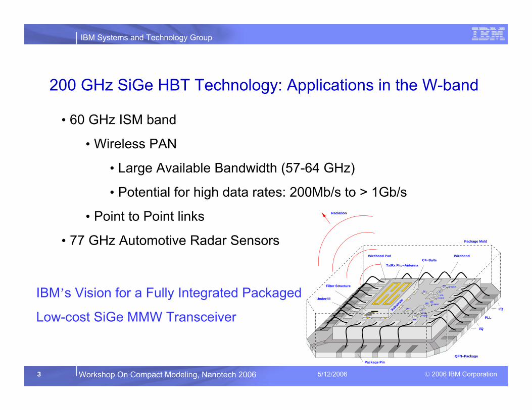
200 GHz SiGe HBT Technology: Applications in the W-band
• 60 GHz ISM band
• Wireless PAN
• Large Available Bandwidth (57-64 GHz)
• Potential for high data rates: 200Mb/s to > 1Gb/s
• Point to Point links
• 77 GHz Automotive Radar Sensors
SiGe−Chip
Radiation
I/Q
I/Q
PLL
QFN−Package
Package Mold
Package Pin
Tx/Rx Flip−Antenna
Wirebond Pad Wirebond
Filter Structure
C4−Balls
Substra
te
Underfill
90
MIX
MIX
LNA
I−signal
Q−signal
VCO
90PA
MIX
MIX
Q−signal
I−signal
VCOIBM’s Vision for a Fully Integrated Packaged
Low-cost SiGe MMW Transceiver

© 2006 IBM Corporation4 5/12/2006Workshop On Compact Modeling, Nanotech 2006
IBM Systems and Technology Group
STI
SiGe Base
C CB BE
SIC
Structure of an Advanced SiGe HBT
Emitter
Deep Trenchx
E B C
Ge
x
• Ge ramp and base thickness help in Speed
• SIC tailoring for Breakdown
J.S.Rieh, Proc. of IEEE

© 2006 IBM Corporation5 5/12/2006Workshop On Compact Modeling, Nanotech 2006
IBM Systems and Technology Group
Expected Scope of Model Scalability
p-cell
Performance Type (HP, MP, HB)
Emitter Width (w)
Emitter Length (l)
Emitter Stripes (n)
Multiplicity (m)
Contact Config
(CBE,CEB,..)
Reliability Options
© 2006 IBM Corporation6 5/12/2006Workshop On Compact Modeling, Nanotech 2006
IBM Systems and Technology Group
0
80
160
240
1.E-05 1.E-04 1.E-03 1.E-02
Ic (A)
fT(GHz)
0
10
20
30
1.E-04 1.E-03 1.E-02 1.E-01
Ic (A)
fT (G
Hz)
0
20
40
60
1.E-05 1.E-04 1.E-03 1.E-02
Ic (A)
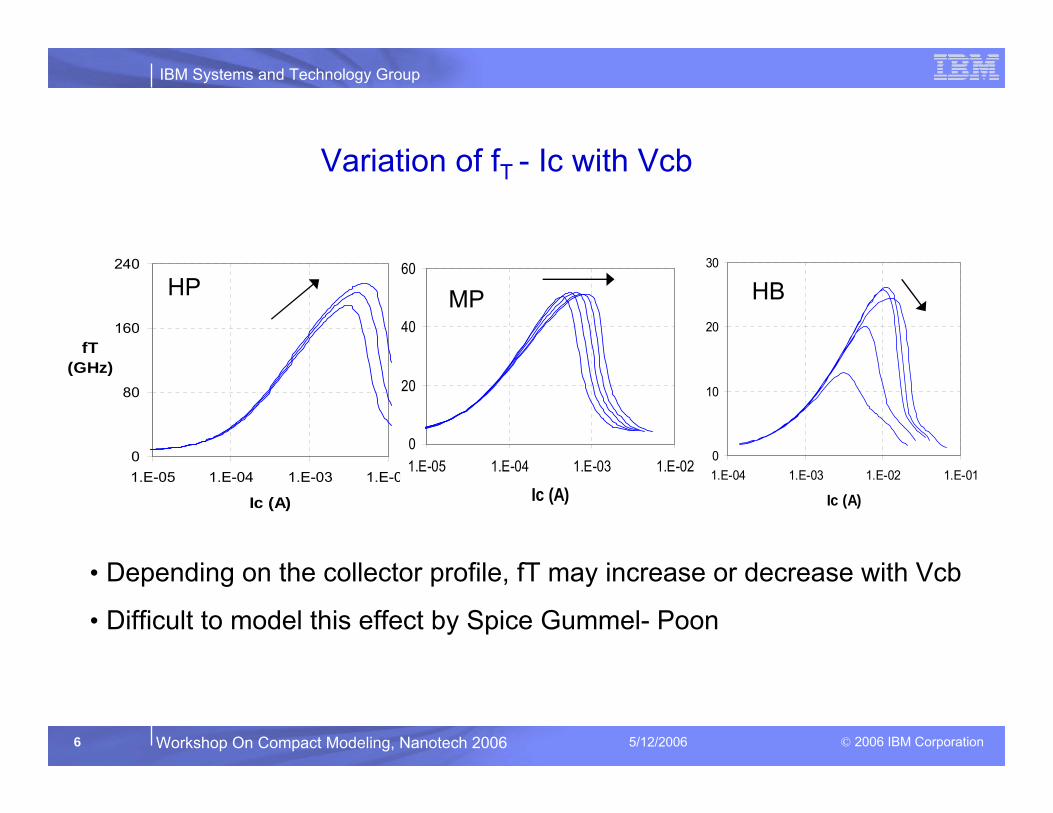
Variation of fT - Ic with Vcb
• Depending on the collector profile, fT may increase or decrease with Vcb
• Difficult to model this effect by Spice Gummel- Poon
HP MP HB

© 2006 IBM Corporation7 5/12/2006Workshop On Compact Modeling, Nanotech 2006
IBM Systems and Technology Group
0
1
2
3
4
0 2 4 6
Vce (V)
Ic (m
A)
0.78
0.82
0.86
0.90
0 2 4 6
Vce (V)
Vbe
(V)
• The BVCEO spans a wide range in a given technology
• The effect of self-heating becomes severe in advanced HBTs
• Quasi-saturation modeling critical for applications using HB devices (eg. PAs)
Avalanche and Self-heating Regimes

© 2006 IBM Corporation8 5/12/2006Workshop On Compact Modeling, Nanotech 2006
IBM Systems and Technology Group
Terminal Resistances 4
Capacitances (BE, BC, CS C-V ) 23
Saturation Currents 22
(Fwd and Inverse, Ideal and non-ideal)
Low current transit time 3
High current transit time 10
Self-heating 2
Avalanche 2
Substrate Transistor/Substrate Network 7
Noise and NQS 5
Temperature coefficients 14
HICUM (High-Current Model) Parameters for Extraction# of parameters

© 2006 IBM Corporation9 5/12/2006Workshop On Compact Modeling, Nanotech 2006
IBM Systems and Technology Group
Methodology
Test Structures: Transistors of various geometries
Specialized Test Structures
Measurements: DC, S-parameters (110GHz)
Model: Hicum 2.1
Parameter Extraction: Matlab
Simulations: Spectre (Cadence)
• Scaling Equations are implemented in Spectre language in the model file

© 2006 IBM Corporation10 5/12/2006Workshop On Compact Modeling, Nanotech 2006
IBM Systems and Technology Group
⎟⎠⎞
⎜⎝⎛
+=
⎟⎠⎞
⎜⎝⎛
+
−=
−=
+=
22121
22121.2
12
)12(2
)12()11(
YYrealRsub
YYimagf
Ccs
fYimagCbc
fYimagYimagCbe
π
π
π
Junction Capacitance Extraction Flow
C B E B C
Cold-S: (i) Vbe=0, vary Vcb (ii) Vcb=0, vary Vbe Total Capacitancefrom Cold-S (Cj)
(On Modeling Transistors)
STI oxide Cap.(Large area Str)
OverlapCapacitance
(Large area Str)
Deembed and Split Cbei into Area & Peri Parts
Cj= CaA + CpP
Area PartC-V fit
Peri Part
C-V fit
C-V Fit

© 2006 IBM Corporation11 5/12/2006Workshop On Compact Modeling, Nanotech 2006
IBM Systems and Technology Group
0.0
1.0
2.0
3.0
-3.0 -2.0 -1.0 0.0
Vbc (V)C
bc (f
F/Sq
um
)
0
25
50
75
100
-1 -0.5 0 0.5 1
Vbe(V)
Cbe
(fF)
HP
MP
HB0.52 μm
3 μm
18 μm
12 μm
)(55.0),(65.0),(95.0)()()(
ln.
000
0
0
HBVSPVHPVVbiHBnSPnHPn
nnkTVbi
nnn
p
n
=>>
⎟⎟⎠
⎞⎜⎜⎝
⎛=
Scaling of Junction Capacitances
zVbiVj
CC⎟⎠⎞⎜
⎝⎛ −
=/1
0
● Data, — Model0.12xL

© 2006 IBM Corporation12 5/12/2006Workshop On Compact Modeling, Nanotech 2006
IBM Systems and Technology Group
Base Resistance Test Structures
C CB2 B1 B2
w
0
300
600
900
1200
0.0 0.1 0.2 0.3
W/dL
Rb
(Ohm
s)Extrinsic BaseResistance
Increasing Vbe
LWrr
IV
R bix
BBb Δ
+=Δ
=2
2,1B1B2
C
E

© 2006 IBM Corporation13 5/12/2006Workshop On Compact Modeling, Nanotech 2006
IBM Systems and Technology Group
Bias Dependence of Base Resistance and
Extraction of Zero-bias Hole Charge in the Base
3000
3500
4000
4500
5000
-0.6 -0.3 0.0 0.3 0.6Vbe (V)
Rbi
(Ohm
/Sq)
250
300
350
Rbx
(Ohm
-um
)
010
QpQjciQjei
rbirbiR +
≈−≡′∫=2
1
1 x
xp
bi
pdxqr
μ
-0.2
0.0
0.2
0.4
-10 0 10
Qj (fC/squm)R
'
Qp0 ~ 60 fC/μm2

© 2006 IBM Corporation14 5/12/2006Workshop On Compact Modeling, Nanotech 2006
IBM Systems and Technology Group
⎥⎦⎤
⎢⎣⎡ −=
VtV
VtV
QQIsi bcbe
ppTT expexp
/ 0 fcfcfbfefefT
rTfTjcijcijeijeippT
QhQQhQ
QQQhQhQQ
++=
++++= 0
1.E-12
1.E-08
1.E-04
1.E+00
0.4 0.7 1.0Vbe (V)
Ic, I
b (A
)
1.E-14
1.E-10
1.E-06
1.E-02
1.E+02
0.4 0.7 1.0
Vbe (V)Ie
, Ib,
Ix (A
)
Transfer Current: Forward and Reverse Gummels

© 2006 IBM Corporation15 5/12/2006Workshop On Compact Modeling, Nanotech 2006
IBM Systems and Technology Group
0.E+00
2.E-03
4.E-03
0.E+00 1.E+03 2.E+03 3.E+03
1/Ic 1/
2.pi
.fT
0
100
200
1.E-04 1.E-03 1.E-02
Ic (A)
fT (G
Hz)
Extraction of Low Current Total Transit Time
jcT
jcjefT
CrercxIcVCC
f)()(
.21
++++=τπ
pCBCBBEEfecf τττττττ ++++==

© 2006 IBM Corporation16 5/12/2006Workshop On Compact Modeling, Nanotech 2006
IBM Systems and Technology Group
( ) ⎟⎠⎞
⎜⎝⎛ −+−Δ+= 111000 c
c bfvlhf ττττ
Extraction of the Low Current Transit Time Components
0
2
4
6
-1.0 0.0 1.0 2.0 3.0Vcb (V)
● Data, — Fit
τ f0
(ps)
Collector τ0(ps) Δτ0h(ps) τbfvl(ps)
HP 0.66 -0.1 0.1
MP 2.2 2.6 2.73
HB 4.9 3.5 6.0
Δτ0h= { τbfvl = carrier jam component
BC SCR Component
Early Effect Component
c = cjci0/cjci
τ0 = predominantly neutral base (not f(V))
HP
HB
MP

© 2006 IBM Corporation17 5/12/2006Workshop On Compact Modeling, Nanotech 2006
IBM Systems and Technology Group
Extraction of the High Current Transit Time Parameters
• Ick: critical current for the onset of high-current effects (base push-out)
• High-current part of the transit time:
• Ick is determined graphically0ff τττ −=Δ
⎟⎟
⎠
⎞
⎜⎜
⎝
⎛ −′+
⎟⎟
⎠
⎞
⎜⎜
⎝
⎛ ′+
′=
PT
ce
ceci
ce
VVV
VV
rVIck lim
2
lim
0
1
1
1
0
2
4
6
8
0.0 0.5 1.0 1.5 2.0
Ic/Ick
Δτ(s
)
0
4
8
12
0.0 0.5 1.0 1.5
Vce (V)
Ick
(mA
)
0
4E-12
8E-12
0.0E+00 8.0E-03 1.6E-02
Ic (A)
Δτ(p
s)
Vcb
Ick1 Ickn
● Data, — Fit

© 2006 IBM Corporation18 5/12/2006Workshop On Compact Modeling, Nanotech 2006
IBM Systems and Technology Group
0.E+00
1.E-04
2.E-04
3.E-04
4.E-04
0.0 0.5 1.0 1.5 2.0
Vce (V)
Ic (A )
0.52 μm
0.E+00
1.E-03
2.E-03
3.E-03
4.E-03
0.0 0.5 1.0 1.5 2.0
Vce (V)
Ic (A)
3 μm
0.E+00
4.E-03
8.E-03
1.E-02
2.E-02
0.0 0.5 1.0 1.5 2.0
Vc e ( V)
I c ( A )
18 μm
Geometry Scaling of the Output Curves
W=0.12 μm W=0.12 μm W=0.12 μm

IBM Systems and Technology Group
© 2005 IBM Corporation9 5/12/2006Workshop on Compact Modeling, Nanotech 2006
0
50
100
150
200
250
1.E-05 1.E-04 1.E-03 1.E-02 1.E-01Ic (A)
fT(GHz)
0
10
20
30
1.E+09 1.E+10 1.E+11 1.E+12
Frequency (GHz)
MA
G/M
SG (d
B)
fT-Vcb and MAG/MSG: Model vs Measurement
Vcb= -0.4, 0, 0.5
Vbe
● Data, — Model

© 2006 IBM Corporation19 5/12/2006Workshop On Compact Modeling, Nanotech 2006
IBM Systems and Technology Group
0
50
100
150
200
250
1.E-05 1.E-04 1.E-03 1.E-02 1.E-01
Ic (A)
fT (G
Hz)
Geometry Scaling of fT-Ic
● Data, — Model
0.52 μm
3 μm
18 μm

© 2006 IBM Corporation20 5/12/2006Workshop On Compact Modeling, Nanotech 2006
IBM Systems and Technology Group
Noise Parameter Simulations
High Frequency Noise Parameter Simulations
• Simulated by SP (with noise) engine in Spectre
2
,min optGGG
n YYGRFF −+=
Fmin : Minimum Noise Figure
Rn: Noise Resistance
YG,opt: The optimum admittance to get minimum noise (GG,opt + jBG,opt)

© 2006 IBM Corporation21 5/12/2006Workshop On Compact Modeling, Nanotech 2006
IBM Systems and Technology Group
0
1
2
3
0.7 0.75 0.8 0.85 0.9 0.95
Vbe(V)
Fmin
(dB
)
0
40
80
120
0.7 0.75 0.8 0.85 0.9 0.95
Vbe (V)
Rn
(Ohm
s)
0
0.4
0.8
0.7 0.75 0.8 0.85 0.9 0.95
Vbe (V)
|Gop
t|
0
40
80
120
0.7 0.75 0.8 0.85 0.9 0.95
Vbe (V)
Phas
e(G
opt)
Noise Parameters: Measurement vs Model (at 18 GHz)
● Data, — Model

© 2006 IBM Corporation22 5/12/2006Workshop On Compact Modeling, Nanotech 2006
IBM Systems and Technology Group
Linearity Measurements and Simulations
Measurements
• Measurements done on an ATN Load pull system
• Tuned for Maximum PAE/ Maximum Pout
• f1=5 GHz, f2 = 5.001 GHz
Simulations
• Harmonic Balance in RFDE (IC51)
• QPSS in Spectre (IC51)
• Simulated 2-tone distortion behavior
2f2-f1
f1 f2
3f2-2f1
• Linearity simulations provide a good check to the accuracy of
the model parameter set and model implementation in the simulator

IBM Systems and Technology Group
© 2005 IBM Corporation10 5/12/2006Workshop on Compact Modeling, Nanotech 2006
pbii qq
qrr
Δ+=
0
00 fjcijeip qqqq +Δ+Δ=Δ, where
0qq p −≤Δ , leads to divide-by-zero errors
We addressed this in ADS2005 by limiting pqΔ
fjcijeip qqqq ++=Δ lim0qq p >Δ
,lim0qq p =Δ lim0qq p ≤Δ
when
when
Improved Rbi Implementation for Better Convergence-1
,0*lim0 qFq −=where .10 << F
A value of F=0.75 is found to provide a good trade-off between convergence and compatibility with the reference implementation.

IBM Systems and Technology Group
© 2005 IBM Corporation11 5/12/2006Workshop on Compact Modeling, Nanotech 2006
[ ]22lim00lim00lim0
0
)(21 δ+−Δ+−Δ+=Δ
++=Δ
qqqqqq
qfqjciqjeiq
ppp
p
Hyperbolic smoothing is applied to the limiting function to eliminate derivative discontinuities at q0lim-
-
Improved Rbi Implementation for Better Convergence-2
Where δ controls the trade-off between smoothness and accuracy. A good choice for δ is d=1e-3*q0’ where q0’ is the parameter describing the temperature-independent part of q0. Derivative expressions are altered as follows:
dTqd
qdqd
dTdq
dqqd
dTqd p
p
ppp 0
0
lim0
lim0
..Δ
Δ
Δ+
Δ=
Δ,. 0
0 bei
p
p
p
bei
p
dVqd
dqqd
dVqd ΔΔ
=Δ

© 2006 IBM Corporation23 5/12/2006Workshop On Compact Modeling, Nanotech 2006
IBM Systems and Technology Group
Inter Modulation Distortion: Measurement vs Model
0
10
20
30
40
-50 -30 -10 10
Pin (dBm)
Ic (m
A)
-0.1
0.3
0.6
0.9
1.2
Ib (m
A)
-40
-20
0
20
-50 -40 -30 -20 -10 0
Pin (dBm)
Pout
(dB
m)
Vbe
• Biased at Vbe = 0.86 V, Vce= 1.36V, corresponds to 35% of peak fTcurrent
• Self-biasing effect is well captured
• Bias dependence is well modeled
● Data, — Model
-120
-70
-20
30
-50 -30 -10 10Pin (dBm)
Pout
, IM
3, IM
5 (d
Bm
)

© 2006 IBM Corporation24 5/12/2006Workshop On Compact Modeling, Nanotech 2006
IBM Systems and Technology Group
Summary
• Most of the important parameters can be extracted by simple
measurements and expressions and fitting routines
• Scaling of these parameters is technology and device layout
dependent
• Hicum 2.1 is able to describe the device characteristics
satisfactorily