Embed Size (px)
Citation preview
External Cavity Diode Lasers:
Controlling Laser Output via Optical Feedback
A thesis submitted in partial fulfillment of the requirement for the degree of Bachelor
of Science with Honors in Physics from the College of William and Mary in Virginia,
by
Matthew Charles Schu
Accepted for ___________________________
(Honors)
Anne C. Reilly
Advisor
Gina L. Hoatson
Todd D. Averett
Robert M. Lewis
Williamsburg, Virginia
April 2003

1
Abstract
Semiconductor diode lasers are widely used in modern technology because of their
compactness, low cost, and durability. However, diode lasers have two major
drawbacks. Light emitted by a diode laser is not monodirectional and typically has a
large bandwidth. While collimating the output of a diode laser is a relatively simple
problem to solve with lenses, narrowing the bandwidth of the output requires
construction of an external cavity. In this project we have created an external cavity
diode laser (ECDL), which selects a single wavelength from the entire output
spectrum of the diode laser and drives the laser at this wavelength. Thus, by using
optical feedback from a diffraction grating, we are able to narrow the total bandwith
emitted by the diode laser. We have characterized the tuning of this laser and show
how the laser can be used to conduct research and also teach students the
fundamentals of laser physics and semiconductor applications.
2
Table of contents
Acknowledgements . . . . . . . . . . . . . . . . . . . . . . . . . . . . . . . . . . . . . . . . . . . . . . . . . 4
1.0 Introduction . . . . . . . . . . . . . . . . . . . . . . . . . . . . . . . . . . . . . . . . . . . . . . . . . . . 5
2.0 Physics Background . . . . . . . . . . . . . . . . . . . . . . . . . . . . . . . . . . . . . . . . . . . . . 6
2.1 General Principle of Lasers . . . . . . . . . . . . . . . . . . . . . . . . . . . . . . . . . 6
2.2 Semiconductor Physics . . . . . . . . . . . . . . . . . . . . . . . . . . . . . . . . . . . . 11
2.3 Semiconductor Diode Lasers . . . . . . . . . . . . . . . . . . . . . . . . . . . . . . . 14
2.4 The External Cavity Diode Laser . . . . . . . . . . . . . . . . . . . . . . . . . . . . 15
3.0 Experiment . . . . . . . . . . . . . . . . . . . . . . . . . . . . . . . . . . . . . . . . . . . . . . . . . . . . 18
3.1 Description of Materials and Setup. . . . . . . . . . . . . . . . . . . . . . . . . . . 18
3.2 Operating the External Cavity Diode Laser . . . . . . . . . . . . . . . . . . . 21
3.3 Measuring Intense Output from ECDL . . . . . . . . . . . . . . . . . . . . . . . 24
4.0 Data Collection and Analysis . . . . . . . . . . . . . . . . . . . . . . . . . . . . . . . . . . . . . 25
4.1 Output Power vs. Drive Current . . . . . . . . . . . . . . . . . . . . . . . . . . . . 25
4.2 Tunable Lasing Modes . . . . . . . . . . . . . . . . . . . . . . . . . . . . . . . . . . . 26
4.3 Stable Range vs. Current . . . . . . . . . . . . . . . . . . . . . . . . . . . . . . . . . 27
4.4 Selected Wavelength vs. Angular Position . . . . . . . . . . . . . . . . . . . . 29
5.0 Conclusions and Future Work . . . . . . . . . . . . . . . . . . . . . . . . . . . . . . . . . . . 30
5.1 Comments on Results . . . . . . . . . . . . . . . . . . . . . . . . . . . . . . . . . . . . . 30
5.2 Future Study and Use of the System . . . . . . . . . . . . . . . . . . . . . . . . . 32
References . . . . . . . . . . . . . . . . . . . . . . . . . . . . . . . . . . . . . . . . . . . . . . . . . . . . . . 33

3
List of Figures
Figure 1 : Three tier laser medium . . . . . . . . . . . . . . . . . . . . . . . . . . . . . . . . . . . 9
Figure 2 : Diagram of ruby laser . . . . . . . . . . . . . . . . . . . . . . . . . . . . . . . . . . . . 10
Figure 3 : Energy band diagram . . . . . . . . . . . . . . . . . . . . . . . . . . . . . . . . . . . . . 12
Figure 4 : Band diagram of an insulator and a metal . . . . . . . . . . . . . . . . . . . 13
Figure 5 : Band diagram of semiconductors . . . . . . . . . . . . . . . . . . . . . . . . . . . 14
Figure 6 : Collimating lens . . . . . . . . . . . . . . . . . . . . . . . . . . . . . . . . . . . . . . . . . 16
Figure 7 : Diagram of constructed ECDL . . . . . . . . . . . . . . . . . . . . . . . . . . . . . 20
Figure 8 : Current vs. Power . . . . . . . . . . . . . . . . . . . . . . . . . . . . . . . . . . . . . . . 25
Figure 9 : Attainable Lasing Modes . . . . . . . . . . . . . . . . . . . . . . . . . . . . . . . . . 26
Figure 10: Maximum Stable Wavelength vs. Current . . . . . . . . . . . . . . . . . . . . 29
Figure 11: Output as a Function of Angle . . . . . . . . . . . . . . . . . . . . . . . . . . . . . 30
4
Acknowledgements
First of all, I would like to thank my advisor, Prof. Anne Reilly of William and Mary,
for guiding me through my first long term research project in physics. Prof. Reilly
was a constant source of help for me and I thank her for giving me her time and
patience. I would also like to thank some other members of the William and Mary
community; Kirk Jacobs in the machine shop for allowing me to use the shop tools
and for his expertise in creating several of our components; Keoki Seu for his help
and advice in the lab; Prof. Gina Hoatson for reminding me of important deadlines
that I was not supposed to miss; and Prof. Todd Averett and Prof. Robert Lewis for
agreeing to be on my defense committee. I would also like to thank Prof. Kane and
Prof. Kossler and their students; Carson Davis, Drew Donnelly, Jack Simonson, Kyle
Wisian, and Jim Younkin, for working my project into their advance laboratory class
for physics and giving me excellent feedback, which helped me prepare for my
defense. Finally, I would like to thank the College of William and Mary for
providing me with the space and materials I needed to conduct this thesis project.
5
1.0 Introduction Because of their small size, low cost, and durability, semiconductor diode lasers are
common in such devices as CD players, laser pointers, and telecommunication
machinery. Recent discoveries of ways to refine the output of diode lasers, which is
naturally very divergent and has a large bandwidth, have allowed these lasers to be
used even in research applications such as atomic spectroscopy, where a precise
tunable light source is required[1]. One of the outcomes of these discoveries is more
cost effective laboratory equipment. A tunable diode laser system costs on the order
of one thousand dollars while a tunable dye laser system can costs tens of thousands
of dollars. Consequently, diode laser systems can be used to open up new areas of
research for small laboratories and also make tunable lasers accessible to educators
and students.
While collimating the output of a diode laser is a relatively simple problem
with lenses, narrowing the bandwidth of the output involves more complicated
physics. In this thesis work we have constructed an external cavity diode laser, which
selects a single wavelength from the entire output spectrum of the diode laser using a
diffraction grating and drives the laser at this wavelength. Using this form of optical
feedback we demonstrate control over the laser wavelength. In this work we have
studied the laser output parameters, wavelength and power, as a function of the laser
input and cavity parameters, current and grating angle.
6
2.0 Physics Background 2.1 General Principles of Lasers
This thesis work relies heavily on exploiting the properties of semiconductor
diode lasers. Before we can begin to discuss these properties, it is necessary to
understand the basics of lasers in general. The term laser is an acronym for Light
Amplification by Stimulated Emission of Radiation. Unlike light from standard
sources such as light bulbs, laser light is coherent. In a perfectly coherent beam of
light all of the photons composing the beam propagate is the same direction, are all of
the same wavelength, and have same phase. In order to construct a laser system one
must have three basic components: an active medium, an excitation source and a laser
cavity. The excitation source and the active medium must be chosen so that the
source creates a population inversion of electrons in the medium. As in most
materials, the electrons of the active medium of any given laser tend to stay at or near
their ground state energy levels in the absence of excitation. Excitation can be
accomplished either by introducing thermal or electronic energy (hear or a current),
or using light of a certain wavelength to excite electrons into higher orbitals, thereby
putting the atoms in higher energy states. This process of exciting electrons up to
higher energy states is often referred to as pumping. Once an electron is excited up to
a higher energy level, it has a tendency to jump back down to its previous lower
energy state. If the rate a which electrons are pumped into the higher energy levels is
faster than the natural time it takes for the electrons to degenerate to their ground
states a population inversion is created in the active medium. Simply stated, a
population inversion occurs when more electrons are being excited to higher energy

7
states of a medium than the system can remove from these higher energy levels via
natural decay.
When the electron in the higher energy state decays down to its lower energy
state it emits some form of energy to preserve the principle of energy conservation.
Quantum mechanics tells us that this energy takes the form of another photon, and
moreover that this energy of this photon must equal the energy difference between
atomic energy states:
E2 � E1 = hν (1)
where E2 and E1 are the excited and the unexcited energy levels of the electron,
respectively, h is Plank�s constant, and ν is the frequency of the photon. Thus, the
frequency, and therefore the wavelength, of the emitted photon are entirely
predictable if one knows the initial and final energy states of the electron.
The direction of the propagating photon, however, is not predictable. How
then does this process lead to coherent light sources that are characteristic of laser
light? To answer this we must differentiate between spontaneous and stimulated
emission of photons. Spontaneous emission of photons involves electrons randomly
decaying from higher energy levels to lower energy levels. This process does not
produce coherent light. In stimulated emission, an incoming photon initiates the
decay or transition of an electron from an excited level to a lower level, causing it to
emit a photon which is a replica of itself. This stimulated emission is a product of the
quantum mechanical nature of the active medium. The region between the ground
state of the electrons and the allowed higher energy states is quantum mechanically
forbidden to the electron. To describe transitions between these states we use

8
probability models. Thus given the existence of an incoming photon, an electron in
the ground state has a certain probability of moving across the forbidden quantum
mechanical barrier into the higher level energy state. The probability of transition is
independent of the direction of the motion across this barrier. Therefore, an electron
that is already in the higher state has the same probability of moving into the ground
state given an incoming photon as an electron in the ground state has of moving into
the higher energy state. For a complete explanation of this phenomenon we refer to
Griffiths� Introduction to Quantum Mechanics [2]. For this discussion, all that one
needs to know about the process of stimulated emission is that the photon given off
by this induced decay to the ground state is of the same frequency and direction of the
photon that induced the change. The initial photon is never absorbed by the electron.
Consequently, the number of photons moving in the same direction with a given
frequency doubles after the induced energy level jump.
The coherent light of a laser is achieved by coupling our active medium with a
laser cavity. The cavity selects some of the photons emitted spontaneously to
repropagate through the medium. The only photons allowed to repropagate through
the medium are those having a wavelength that satisfies the equation:
λn = 2L/n (2)
where L is the length of the laser cavity, n is the harmonic mode of the wave. Thus,
the cavity allows only photons whose wavelength can form a standing wave in the
cavity, which limits the wavelength, phase, and direction of the photons allowed to
repropagate through the medium. These photons induce other photons of the same
propagating direction, phase and wavelength via stimulated emission, and in a brief
9
time all the photons propagating through the cavity are coherent. To get this
coherent light out of the cavity and make use of it, one only needs to make one of the
reflective end of the cavity semi-reflective, thus allowing some of the coherent light
to escape. The rate at which photons are randomly absorbed or exit through the semi-
reflective ends of the cavity is called loss. The rate at which the photons give rise to
other photons via stimulated emission is call gain. To have a functioning laser our
gain versus loss ratio must be greater than one.
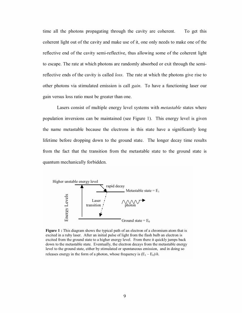
Lasers consist of multiple energy level systems with metastable states where
population inversions can be maintained (see Figure 1). This energy level is given
the name metastable because the electrons in this state have a significantly long
lifetime before dropping down to the ground state. The longer decay time results
from the fact that the transition from the metastable state to the ground state is
quantum mechanically forbidden.
Higher unstable energy level rapid decay
Metastable state = E1
Laser
transition photon
Ground state = E0
Figure 1 : This diagram shows the typical path of an electron of a chromium atom that is excited in a ruby laser. After an initial pulse of light from the flash bulb an electron is excited from the ground state to a higher energy level. From there it quickly jumps back down to the metastable state. Eventually, the electron decays from the metastable energy level to the ground state, either by stimulated or spontaneous emission, and in doing so releases energy in the form of a photon, whose frequency is (E1 � E0)/h.
Ener
gy L
evel
s
10
Typical decay times of allowed transitions take about a microsecond or less.
Transitions across forbidden energy regions may take one thousand to one million
times longer depending on the size of the energy gap[3].
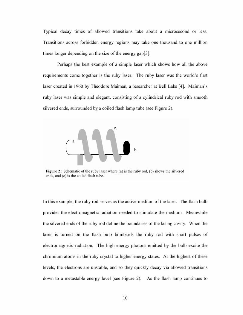
Perhaps the best example of a simple laser which shows how all the above
requirements come together is the ruby laser. The ruby laser was the world�s first
laser created in 1960 by Theodore Maiman, a researcher at Bell Labs [4]. Maiman�s
ruby laser was simple and elegant, consisting of a cylindrical ruby rod with smooth
silvered ends, surrounded by a coiled flash lamp tube (see Figure 2).
In this example, the ruby rod serves as the active medium of the laser. The flash bulb
provides the electromagnetic radiation needed to stimulate the medium. Meanwhile
the silvered ends of the ruby rod define the boundaries of the lasing cavity. When the
laser is turned on the flash bulb bombards the ruby rod with short pulses of
electromagnetic radiation. The high energy photons emitted by the bulb excite the
chromium atoms in the ruby crystal to higher energy states. At the highest of these
levels, the electrons are unstable, and so they quickly decay via allowed transitions
down to a metastable energy level (see Figure 2). As the flash lamp continues to
c. b. Figure 2 : Schematic of the ruby laser where (a) is the ruby rod, (b) shows the silvered ends, and (c) is the coiled flash tube.
a.
11
pulse, more and more electrons get �stuck� in metastable energy level due to the
slower decay rate, and a population inversion is created. When electrons finally do
make the jump from the metastable state down to the ground state, they give off a
photon of a precise frequency as discussed before. These photons are reflected
through the active medium by the silvered ends of the ruby. Some escape the cavity
and produce the laser�s beam of light. Others induce other photons via stimulated
emission before eventually escaping or being absorbed by an atom in the crystal.
After the success of the first ruby laser, research in the field of lasers took off
at an amazing rate. Today we have lasers that produce coherent beams of a wide
range of wavelengths using a variety of mediums. The work of this thesis, however,
deals specifically with semiconductor diode lasers. In order to understand how these
devices function, it is necessary to understand the basics of semiconductor physics.
2.2 Semiconductor Physics
The unique distribution of electrons in atoms is what makes some materials
good conductors, other materials poor conductors, and still other materials
semiconductors. Each electron in an atom has a net energy value that comes from the
sum of its kinetic and potential energies. We know from quantum mechanics that
each electron's energy is not random. Rather, there are defined regions of allowed and
unallowed energy states about the nucleus that constrain the �choice� of energies for
a given electron. Moreover, from the Pauli Exclusion Principle we know that not
more than two electrons, each with opposite spins, can occupy a given state the same
time. When atoms are brought together to form a solid, the individual energy states
12
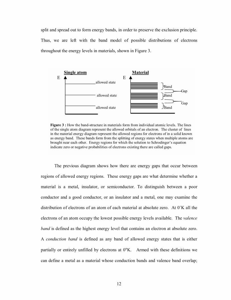
split and spread out to form energy bands, in order to preserve the exclusion principle.
Thus, we are left with the band model of possible distributions of electrons
throughout the energy levels in materials, shown in Figure 3.
The previous diagram shows how there are energy gaps that occur between
regions of allowed energy regions. These energy gaps are what determine whether a
material is a metal, insulator, or semiconductor. To distinguish between a poor
conductor and a good conductor, or an insulator and a metal, one may examine the
distribution of electrons of an atom of each material at absolute zero. At 0ûK all the
electrons of an atom occupy the lowest possible energy levels available. The valence
band is defined as the highest energy level that contains an electron at absolute zero.
A conduction band is defined as any band of allowed energy states that is either
partially or entirely unfilled by electrons at 0°K. Armed with these definitions we
can define a metal as a material whose conduction bands and valence band overlap;
Single atom Material E E allowed state Band Gap allowed state Band
Gap allowed state Band
Figure 3 : How the band-structure in materials form from individual atomic levels. The lines of the single atom diagram represent the allowed orbitals of an electron. The cluster of lines in the material energy diagram represent the allowed regions for electrons of in a solid known as energy band. These bands form from the splitting of energy states when multiple atoms are brought near each other. Energy regions for which the solution to Schrodinger�s equation indicate zero or negative probabilities of electrons existing there are called gaps.
13
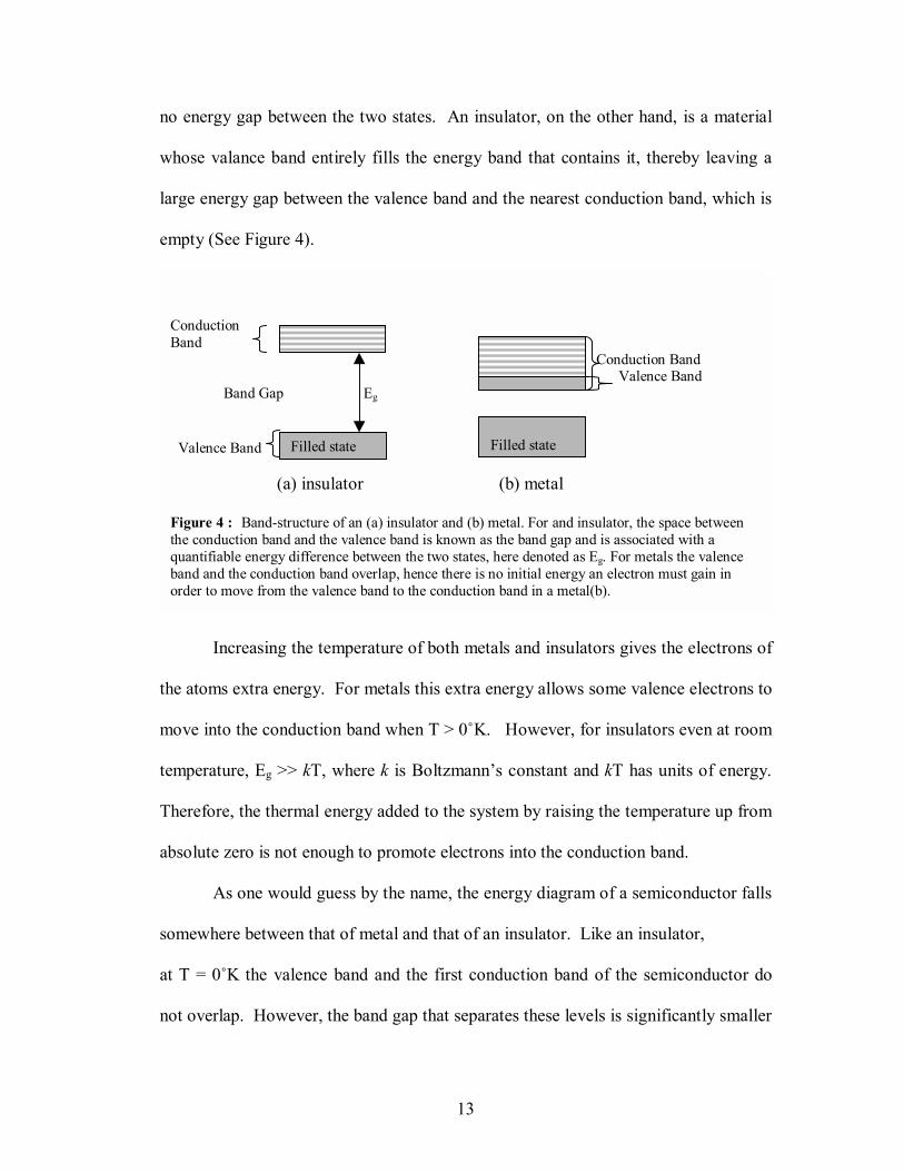
no energy gap between the two states. An insulator, on the other hand, is a material
whose valance band entirely fills the energy band that contains it, thereby leaving a
large energy gap between the valence band and the nearest conduction band, which is
empty (See Figure 4).
Increasing the temperature of both metals and insulators gives the electrons of
the atoms extra energy. For metals this extra energy allows some valence electrons to
move into the conduction band when T > 0ûK. However, for insulators even at room
temperature, Eg >> kT, where k is Boltzmann�s constant and kT has units of energy.
Therefore, the thermal energy added to the system by raising the temperature up from
absolute zero is not enough to promote electrons into the conduction band.
As one would guess by the name, the energy diagram of a semiconductor falls
somewhere between that of metal and that of an insulator. Like an insulator,
at T = 0ûK the valence band and the first conduction band of the semiconductor do
not overlap. However, the band gap that separates these levels is significantly smaller
Conduction Band Conduction Band Valence Band Band Gap Eg Valence Band (a) insulator (b) metal Figure 4 : Band-structure of an (a) insulator and (b) metal. For and insulator, the space between the conduction band and the valence band is known as the band gap and is associated with a quantifiable energy difference between the two states, here denoted as Eg. For metals the valence band and the conduction band overlap, hence there is no initial energy an electron must gain in order to move from the valence band to the conduction band in a metal(b).
Filled state Filled state
14
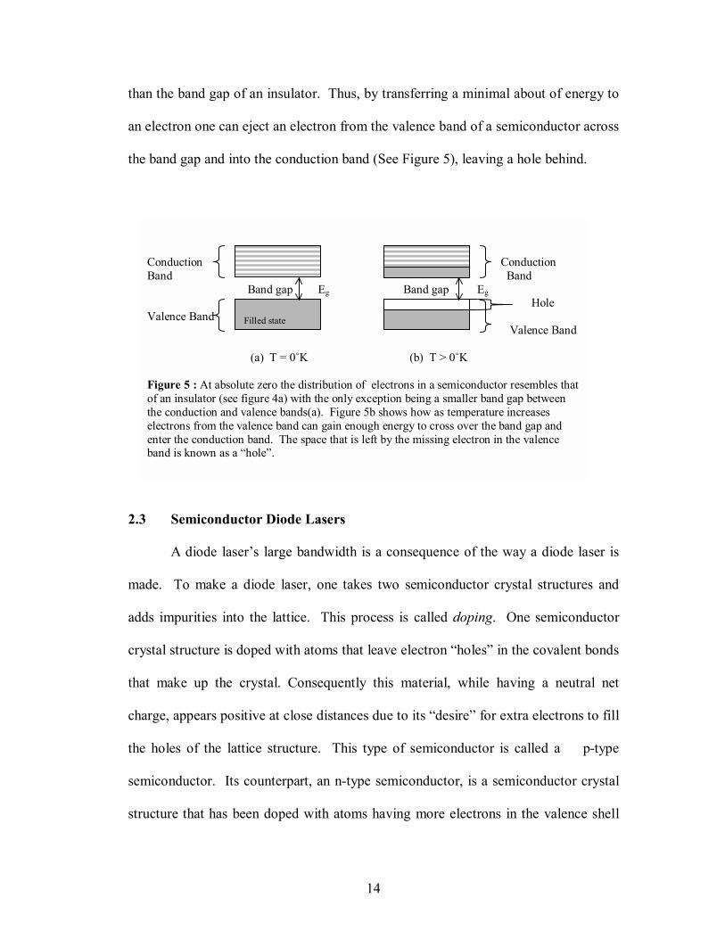
than the band gap of an insulator. Thus, by transferring a minimal about of energy to
an electron one can eject an electron from the valence band of a semiconductor across
the band gap and into the conduction band (See Figure 5), leaving a hole behind.
2.3 Semiconductor Diode Lasers
A diode laser�s large bandwidth is a consequence of the way a diode laser is
made. To make a diode laser, one takes two semiconductor crystal structures and
adds impurities into the lattice. This process is called doping. One semiconductor
crystal structure is doped with atoms that leave electron �holes� in the covalent bonds
that make up the crystal. Consequently this material, while having a neutral net
charge, appears positive at close distances due to its �desire� for extra electrons to fill
the holes of the lattice structure. This type of semiconductor is called a p-type
semiconductor. Its counterpart, an n-type semiconductor, is a semiconductor crystal
structure that has been doped with atoms having more electrons in the valence shell
Conduction Conduction Band Band Band gap Eg Band gap Eg Hole Valence Band Valence Band (a) T = 0ûK (b) T > 0ûK Figure 5 : At absolute zero the distribution of electrons in a semiconductor resembles thatof an insulator (see figure 4a) with the only exception being a smaller band gap between the conduction and valence bands(a). Figure 5b shows how as temperature increases electrons from the valence band can gain enough energy to cross over the band gap and enter the conduction band. The space that is left by the missing electron in the valence band is known as a �hole�.
Filled state

15
than the atoms of the crystal which they replace. These impurities give the
semiconductor a negative appearance at close distances due to its willingness to give
up the extra electrons not used in the covalent bonding of the crystal lattice. When a
p-type and an n-type semiconductor are joined together the result is called a p-n
junction. Applying a voltage across this junction creates a diode. If a voltage is
applied in the right direction current flows through the pn-junction and as it does
electrons in high energy states in the n-type lattice find holes as they move across the
p-n junction. When an electron finds a hole, it decays down to a lower energy state,
releasing a photon. The energy released as an electron drops down into a hole
depends on the size of the energy gap an electron crosses to combine with a hole.
This gap distance depends on three things: the type of semiconductors used to make
the diode, the thermal energy inside the diode, and the way in which the p and n-type
semiconductors are joined together. The faces of the semiconductor crystals are
made reflective by either coatings or the cut of the crystal. The reflective ends create
the laser cavity, the final component of our laser[5]. Since the size of a standard
diode laser cavity is about 1mm in length, one can see (using Equation 2) that the
difference between allowed wavelengths in the laser cavity are very small. For
example, if λn = 700nm and L = 1mm, then Equation 2 gives the next allowed
wavelength λn+1 ≈ 699.8nm, making ∆λ=0.2nm. This property of the diode laser
causes the laser to emit multiple wavelengths of light.
2.4 The External Cavity Diode Laser (ECDL)
Another drawback of working with diode lasers is that, unlike other types of
lasers, the light emitted by a diode laser greatly diverges in an oval shape pattern with
16
the highest spread of light at an angle of about 25 degrees. Such a wide beam is
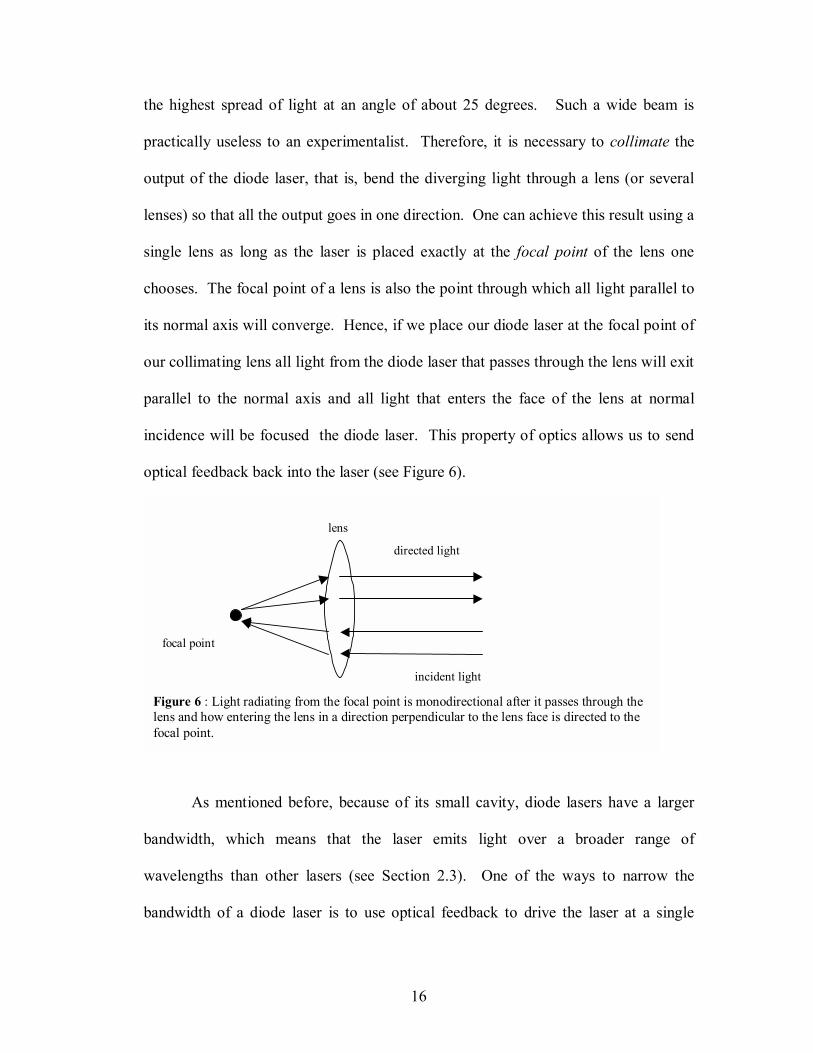
practically useless to an experimentalist. Therefore, it is necessary to collimate the
output of the diode laser, that is, bend the diverging light through a lens (or several
lenses) so that all the output goes in one direction. One can achieve this result using a
single lens as long as the laser is placed exactly at the focal point of the lens one
chooses. The focal point of a lens is also the point through which all light parallel to
its normal axis will converge. Hence, if we place our diode laser at the focal point of
our collimating lens all light from the diode laser that passes through the lens will exit
parallel to the normal axis and all light that enters the face of the lens at normal
incidence will be focused the diode laser. This property of optics allows us to send
optical feedback back into the laser (see Figure 6).
As mentioned before, because of its small cavity, diode lasers have a larger
bandwidth, which means that the laser emits light over a broader range of
wavelengths than other lasers (see Section 2.3). One of the ways to narrow the
bandwidth of a diode laser is to use optical feedback to drive the laser at a single
focal point
lens
incident light
directed light
Figure 6 : Light radiating from the focal point is monodirectional after it passes through the lens and how entering the lens in a direction perpendicular to the lens face is directed to the focal point.
17
allowed lasing frequency. As previously discussed, the collimation lens of the ECDL
is one critical part of attaining optical feedback. The second part of our system that
allows optical feedback is the diffraction grating. A diffraction grating is finely
scored reflective material that, due to its geometry, allows only certain wavelengths
of light incident at an angle θ to interfere constructively with itself as it is reflected
outward. The formula for constructively diffracted orders of light reflected from a
diffraction grating is:
d sinθ = m λ (3)
where d is the spacing between reflective surfaces, θ is the angle of incidence, λ is the
wavelength of the incident light and m is an integer[6]. One consequence of the
above equation for is that spectra diffracted off a grating are reproduced at several
different angular positions about the grating. The various replications of the spectra
are called orders of diffraction and obey the following relationship.
(sin θi + sin θm)= N m λ (4)
where θm is the angle of the mth order diffracted beam, N is the spatial frequency of
the grating (units nm-1), and θi, m, λ are incident angle, integer, and wavelength as
before[7].
18
3.0 Experiment 3.1 Description of Materials and Setup
The key components of this external cavity diode laser (ECDL) setup are a
current driver, a standard 9mm diode laser of the 780nm range, a collimating lens, a
diffraction grating, two kinematic optical mounts, an Ocean Optics S2000
spectrometer, and two digital multimeters used to monitor the input current the and
the power of the laser output. In this thesis work, the construction began with the
housing for the Thorlabs laser diode current driver (model LD1255). The driver is a
small circuit board roughly 8cm x 3.5cm in size and is about 1.0cm thick when all the
electrical components are mounted onto it. Consequently, the housing for the driver
is only of modest size, 15cm x 5cm x 7cm. The benefits to using this particular driver
include the ability to vary the input current both internally and externally by
electronic control, and the ability to monitor the input current and output power
simultaneously. The next critical piece of the setup is the laser housing. The
housing consists of a three prong 9mm diode laser socket placed in a kinematic mirror
mount from Thorlabs (product number : KC1-T), which as three independent
adjusters on the back to change the angle. By wiring our laser driver to a three-prong
socket rather than directly to the diode laser, one can easily replace the diode laser
within the system and thus have the ability to diodes of different ranges of
wavelengths. The lens used is an aspheric collimating lens of focal length 5mm, and
it is mounted to a 35 mm cage plate, CP03 (from Thorlabs). The optical feedback of
the system is controlled by a 12.7mm gold diffraction grating from Edmund Optics
having a coarseness of 1200 grooves per millimeter. Like the laser diode, the
19
diffraction grating is placed on a mount whose angle can be finely adjusted by three
screws on the back. Before securing the diffraction grating on our kinematic mount,
the grating is first affixed to a cylindrical piece of Lucite, which at one end has a
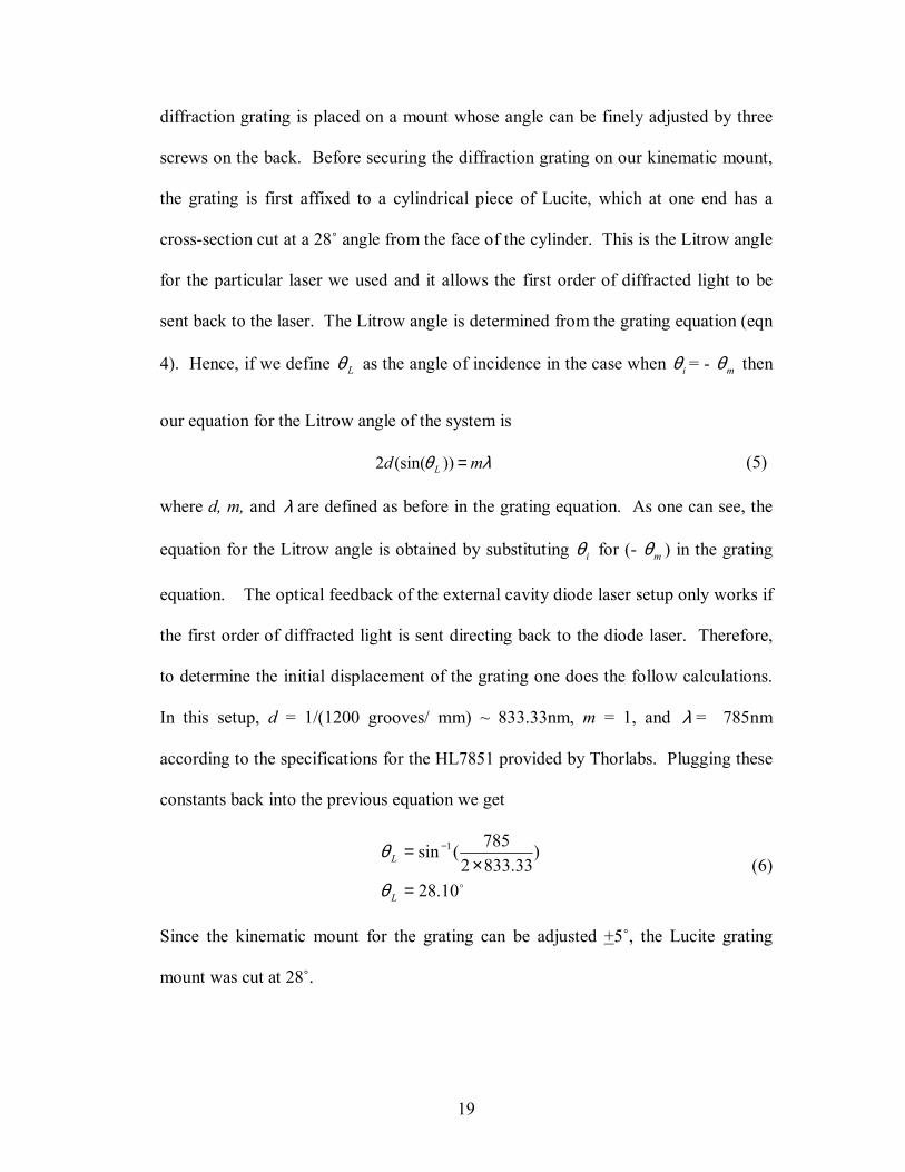
cross-section cut at a 28û angle from the face of the cylinder. This is the Litrow angle
for the particular laser we used and it allows the first order of diffracted light to be
sent back to the laser. The Litrow angle is determined from the grating equation (eqn
4). Hence, if we define Lθ as the angle of incidence in the case when iθ = - mθ then
our equation for the Litrow angle of the system is
λθ md L =))(sin(2 (5)
where d, m, and λ are defined as before in the grating equation. As one can see, the
equation for the Litrow angle is obtained by substituting iθ for (- mθ ) in the grating
equation. The optical feedback of the external cavity diode laser setup only works if
the first order of diffracted light is sent directing back to the diode laser. Therefore,
to determine the initial displacement of the grating one does the follow calculations.
In this setup, d = 1/(1200 grooves/ mm) ~ 833.33nm, m = 1, and λ = 785nm
according to the specifications for the HL7851 provided by Thorlabs. Plugging these
constants back into the previous equation we get
o10.28
)33.8332
785(sin 1
=×
= −
L
L
θ
θ (6)
Since the kinematic mount for the grating can be adjusted +5û, the Lucite grating
mount was cut at 28û.
20
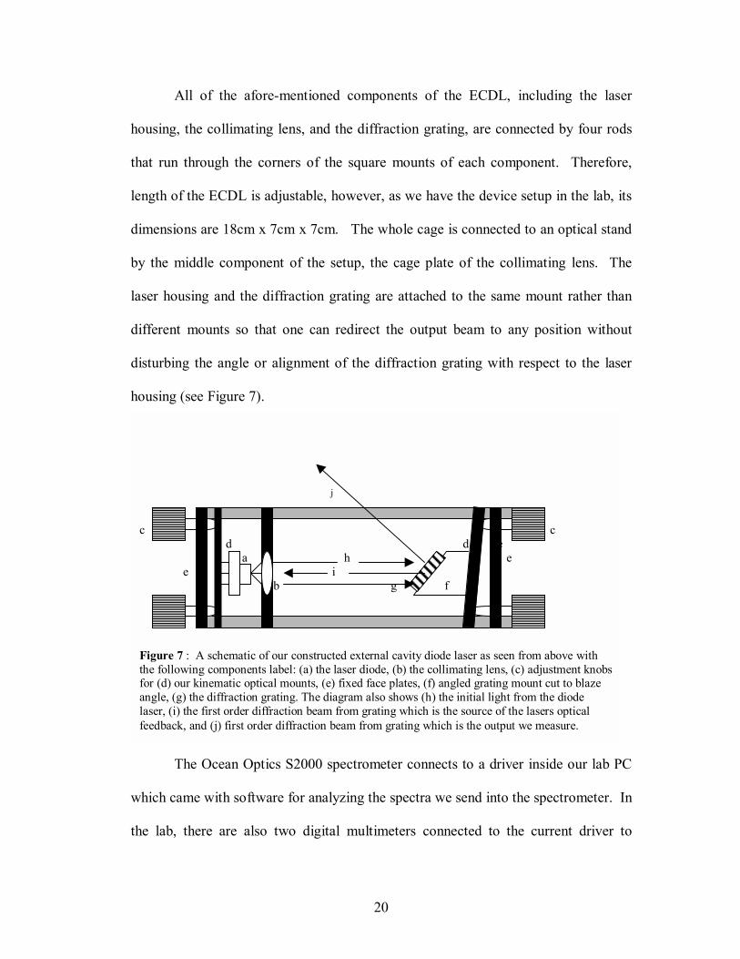
All of the afore-mentioned components of the ECDL, including the laser
housing, the collimating lens, and the diffraction grating, are connected by four rods
that run through the corners of the square mounts of each component. Therefore,
length of the ECDL is adjustable, however, as we have the device setup in the lab, its
dimensions are 18cm x 7cm x 7cm. The whole cage is connected to an optical stand
by the middle component of the setup, the cage plate of the collimating lens. The
laser housing and the diffraction grating are attached to the same mount rather than
different mounts so that one can redirect the output beam to any position without
disturbing the angle or alignment of the diffraction grating with respect to the laser
housing (see Figure 7).
The Ocean Optics S2000 spectrometer connects to a driver inside our lab PC
which came with software for analyzing the spectra we send into the spectrometer. In
the lab, there are also two digital multimeters connected to the current driver to
j c c d d e
a h e e i b g f Figure 7 is a schematic of our constructed external cavity diode laser as seen from above with the following components labeled: (a) the laser diode, (b) the collimating lens, (c) adjustment knobs for (d) our kinematic optical mounts, (e) fixed face plates, (f) angled grating mount cut to blaze angle, (g) the diffraction grating. The diagram also shows (h) the initial light from the diode laser, (i) the zero order diffraction beam from grating which is the source of the laser�s optical feedback, and (j)zero order diffraction beam from grating which is the output we measure.
j c c d d e
a h e e i b g f Figure 7 : A schematic of our constructed external cavity diode laser as seen from above with the following components label: (a) the laser diode, (b) the collimating lens, (c) adjustment knobs for (d) our kinematic optical mounts, (e) fixed face plates, (f) angled grating mount cut to blaze angle, (g) the diffraction grating. The diagram also shows (h) the initial light from the diode laser, (i) the first order diffraction beam from grating which is the source of the lasers optical feedback, and (j) first order diffraction beam from grating which is the output we measure.

21
monitor current across the diode laser and the output power. The resolution of the
spectrometer is 1nm, while the resolution of the digital multimeters is 0.1mA.
3.2 Operating the External Cavity Diode Laser
To operate the ECDL one first selects a diode laser with the appropriate
bandwidth. Since some of the laser�s output will be retroreflected back into the
cavity, it is important to choose a laser diode with highly reflective coating on the
back face and a reduced reflectivity coating on the output face. While many low
power diode lasers do not have such coatings, diode lasers that produce 30mW or
more output power generally have these extra coatings[8]. In this experiment an
HL7851 785nm laser diode with an output power rating of 50mW was used. The
HL7851 was placed into the three-prong diode socket on the laser mount. Since all
laser diodes are extremely sensitive to static electricity and can be shorted out by
sudden spikes of current, it is important to turn the internal variable resistor (pot) all
the way to its highest resistance setting before the current driver is turned on. Once
this is so, one should turn slowly increase the amount of current through the system
by slowly turning the pot until the input current is just above the threshold current, or
the minimum current value at which the diode laser lases. At this point the laser
needs to sit for about 1 hour until the system achieves thermal equilibrium (i.e., it has
to warm up) since the thermal energy of the semiconductor material significantly
affects the energy of the photons that are emitted by the diode laser.
While waiting, the laser output is collimated by adjusting the laser until it is
exactly 1 focal length from the collimating lens. In practice the best way to see if the
22
laser is at the focal point of the lens is to remove the back half of the ECDL, which is
the diffraction grating and mount, and aim the entire laser housing at a distant wall to
see if the spread of the output beam on the wall is the same size as the spread
produced by shining the laser on a piece of paper right in front of the setup. It is
possible for one to have agreement in the size of the light beam on the wall and that
of the beam on the piece of paper and still have the output not collimated. Therefore,
one should examine the spread of the laser beam on the piece of paper when the paper
is at several different points between the laser diode and the wall. If the size of the
spread is constant regardless of the position of the paper, then the laser is collimated.
Aside from being collimated, it is also desirable to have the output from the laser
level with the horizontal plane. Since the laser is on a kinematic mount, it is easy to
make sure the collimated beam is not angled up or down from the horizontal. The
laser beam must be horizontal so that the first order diffracted beam will be directed
back at the collimating lens rather than above or below it. The tool used to ensure the
beam is parallel to the ground is a simple thin metal panel (Thorlabs) that hangs from
the top rods of our ECDL cage set and has a pin hole located exactly at the height of
the center axis of the cage. By placing the panel on the cage, one can see if the laser
light is skewed from the horizontal axis, using the angle adjusters on the back of the
laser house, and redirect the beam accordingly.
Once the laser beam is collimated, one can replace the grating and mount are
replaced onto the ECDL cage, and the alignment of the laser is rechecked. If the
alignment tool is hanging in the center of the cage setup, two red dots will be seen
from the back (grating side) of the ECDL. One dot is the light coming through the
23
pinhole from the laser diode on the other side. This light reflects off the grating and
creates a second red dot on the panel. What is desired is to have these two dots
overlap entirely. If this is not already so, one can move the second dot by using the
adjustment knobs on the kinematic grating mount. After all the previous alignments
have been made the zero order diffraction coming off the ECDL is directed into the
fiver optic input of the spectrometer.
Even with all the fine tuning that has been done to ensure the light is being
sent back into the laser diode, at this point it is likely that the diffracted beam is still
not being sent directly into the diode laser�s small cavity. The way to know one has
succeeded in creating a new source of optical feedback for the diode laser is to watch
the distribution of wavelengths on the spectrometer while slowly adjusting the knobs
on the back of the grating mount.
One of tricks learned to get the alignment close to perfect that helped in this
experiment was to put the fiber optic cable through a hole in a stiff piece of paper,
such that the entire spread of the beam could be seen on the vertical plane. While
observing how the light fell on the plane two somewhat overlapping beams were
noticed; one being slightly fainter than the other. The second, fainter beam came
from the light that was reflected off the collimating lens that had already been
diffracted by the grating. Thus the two distributions came from two light beams that
had traveled two different distances. That the light beams did not line up exactly
indicated that there still was some error in the alignment. By adjusting the kinematic
mounts one can get these beams to overlap.
24
Once certain the light diffracted off the grating is reentering the lasing cavity
of the diode laser, one can use the new extended adjustable cavity to select several
different output wavelengths to study or utilize. To select different wavelength
within the tunable range of the diode laser, one simply adjusts the horizontal angle of
the diffraction grating using a fine adjustment micrometer on the back of the mount.
To understand why changing the angle of the diffraction grating changes the
wavelength of the retroreflected beam, consider the Litrow angle equation (eqn. 5).
We see that when we adjust Lθ we change the allowed wavelength of light that is
directed back into the laser diode. Hence, changing the angle of the diffraction
grating selects a different wavelength at which we drive the lasing process.
3.3 Measuring Intense Output from the ECDL
Initially, we ran into the problem that the unfiltered light from the ECDL was
too intense for our spectrometer to read accurately, making it impossible to determine
where the peak of a distribution was located. To overcome this obstacle we had to
devise a way to cut down on the intensity of the light that was being sent to the fiber
optic receiver without omitting any wavelengths from the spectrum. The solution
was to first reflect the output beam off a normal piece of glass before sending the
beam to the spectrometer.

25
4.0 Data and Analysis 4.1 Output Power versus Current
The threshold current for the HL7851 diode laser was found to be around
40mA. The threshold current is found by setting the internal pot of the laser diode to
zero and then slowly increasing the driver current using the manual pot. Meanwhile,
one watches for light to appear on a flat piece of paper placed in front of the diode
laser. Since the human eye is far more sensitive to photons than most electronic
equipment, finding the threshold current of the diode laser by eye is perfectly
legitimate.
Beyond finding the threshold current it is also useful to know how the laser
power increases as a function of current. To measure the power of our output
spectrum we used an external laser power meter (Molectron AS500). The power
meter was located so that it received the collimated output coming directly from the
diode laser. Figure 8 shows the output power versus input current for the HL7851
laser diode, with the diffraction grating removed.
0
5
10
15
20
50 60 70 80 90 100 110 120 130
Current vs. Power
y = -15.067 + 0.28x R= 0.99908
Out
put P
ower
(m
W)
Drive Current (mA) Figure 8: The relationship between output power and input current. From the threshold current up till roughly 110 mA the plot of the output power vs. current follows a linear trend. However, beyond this region this output is not linear.
26
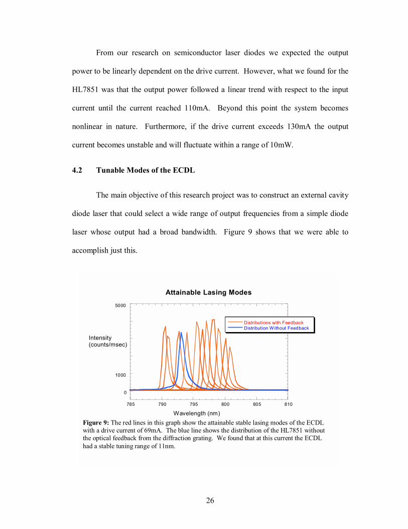
From our research on semiconductor laser diodes we expected the output
power to be linearly dependent on the drive current. However, what we found for the
HL7851 was that the output power followed a linear trend with respect to the input
current until the current reached 110mA. Beyond this point the system becomes
nonlinear in nature. Furthermore, if the drive current exceeds 130mA the output
current becomes unstable and will fluctuate within a range of 10mW.
4.2 Tunable Modes of the ECDL
The main objective of this research project was to construct an external cavity
diode laser that could select a wide range of output frequencies from a simple diode
laser whose output had a broad bandwidth. Figure 9 shows that we were able to
accomplish just this.
0
1000
5000
785 790 795 800 805 810
Attainable Lasing Modes
Distributions with FeedbackDistribution Without Feedback
Intensity(counts/msec)
Wavelength (nm)Figure 9: The red lines in this graph show the attainable stable lasing modes of the ECDL with a drive current of 69mA. The blue line shows the distribution of the HL7851 without the optical feedback from the diffraction grating. We found that at this current the ECDL had a stable tuning range of 11nm.
27
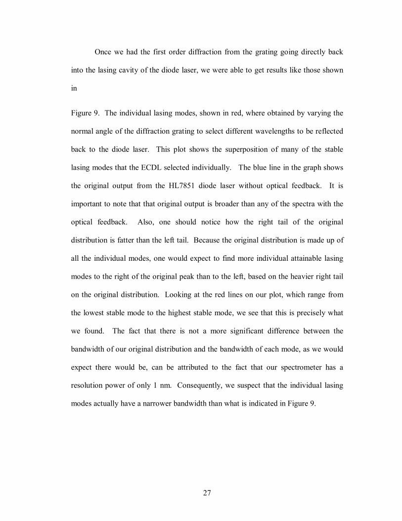
Once we had the first order diffraction from the grating going directly back
into the lasing cavity of the diode laser, we were able to get results like those shown
in
Figure 9. The individual lasing modes, shown in red, where obtained by varying the
normal angle of the diffraction grating to select different wavelengths to be reflected
back to the diode laser. This plot shows the superposition of many of the stable
lasing modes that the ECDL selected individually. The blue line in the graph shows
the original output from the HL7851 diode laser without optical feedback. It is
important to note that that original output is broader than any of the spectra with the
optical feedback. Also, one should notice how the right tail of the original
distribution is fatter than the left tail. Because the original distribution is made up of
all the individual modes, one would expect to find more individual attainable lasing
modes to the right of the original peak than to the left, based on the heavier right tail
on the original distribution. Looking at the red lines on our plot, which range from
the lowest stable mode to the highest stable mode, we see that this is precisely what
we found. The fact that there is not a more significant difference between the
bandwidth of our original distribution and the bandwidth of each mode, as we would
expect there would be, can be attributed to the fact that our spectrometer has a
resolution power of only 1 nm. Consequently, we suspect that the individual lasing
modes actually have a narrower bandwidth than what is indicated in Figure 9.
28
4.3 Stable Range versus Current
To study how semiconductor diode lasers are affected by increases in the
current and the thermal energy across the p-n junction, we next studied how our
tunable range of wavelengths was affected by input current. Figure 10 shows how the
position of the highest stable mode of a given tunable range changed with an
increasing current.
In general, the upper ends of the tunable ranges increase as current
increases. However, the relationship between current and peak wavelength is clearly
not linear. Notice that there is a large jump in peak wavelengths as we move from a
drive current of 75mA to 80mA, but then the peak wavelength barely changes at all
until we push the drive up to 110mA. Such a complex relationship between tunable
range and drive current suggests that calibrating an ECDL such as this one would be
difficult if one wanted to include all possible parameters that could be varied in the
system (see Figure 10).

29
4.4 Selected Wavelength versus Angular Position
The final aspect of our system that we wished to analyze was the angular dependence
of the feedback lasing modes. Using the fine adjustment knob on the back of our
diffraction grating mount, we recorded the change of wavelength versus the Litrow
angle. Since the wavelength that is sent back to the diode laser travels along the path
of the incident beam of light, we expect the relationship between angular
displacement and the wavelength of our output to obey the Litrow angle equation
(eqn 5). The Litrow angle was changed by moving a micrometer which tilted the
grating base plate by a certain distance that we could measure to a level of accuracy
of 1µm. The data are shown on Figure 11. We expect, from looking at Equation 5, a
linear relationship when plotting the wavelength versus 2sin(θ). Moreover, the
0
1000
2000
3000
4000
5000
780 785 790 795 800 805 810 815
Maximum Stable Wavelength vs Current
60 mA
65 mA
70 mA
75 mA
80 mA
80 mA
85 mA
90 mA
95 mA
100 mA
105 mA
110 mA
Intensity counts/msec
Wavelength (nm)
Figure 10: Each peak on this graph represents the highest wavelength in the stable tunable range at a given input current. The different input currents are differentiated by color and pattern and are indicated in the legend to the left. In general, the upper ends of the tunable ranges tend to increase as the current increases.

30
expected slope of the graph is d = 833.33(nm), which is the grating spacing constant
we calculated earlier.
Our results, shown on Figure 11, agreed with our expectations. The absolute value of
the slope of our best fit line was 855.59 (nm) which is within 2.7% of our expected
slope.
5.0 Conclusions and Future Work
5.1 Conclusions After a semester of failed attempts, we finally constructed an external cavity
diode laser that produces a tunable, collimated beam of light. We studied and
characterized the output of the tunable, monochromatic light source we had created,
and from our observations of the ECDL�s output, given variations of certain input
parameters, we determined the following properties about out system. First, we
801
802
803
804
805
806
0.098 0.099 0.1 0.101 0.102 0.103 0.104
Output as a Function of Angle
Wavelength of peak
y = 889.99 - 855.59x R= 0.99878
wavelength(nm)
2*sin( Litrow Angle) Figure 11: This graph shows the relationship between the selected wavelength and the angle of the diffraction grating. The data above agrees with what is predicted by the Litrow angle equation. The drive current for the laser diode while the data was taken was 130 mA.
31
noticed that we could select monochromatic lasing modes from an 11nm range of
possible lasing modes. Tuning the precise wavelength we wanted was fairly easy
with the setup we had. By design, our ECDL has a single knob to control the
horizontal change in the normal angle of the grating. We found that, as predicted by
the Litrow angle equation, the wavelength selected was linearly dependent on the sine
of the Litrow angle.
However, we observed that the laser�s response to a change in current was not
linear. We suspect the system�s complicated response to changes in current stem
from internal characteristics of the diode laser. There appeared to be a linear and
nonlinear region in the graph of laser output power vs. current, and when the system
was driven at higher levels the output power was unstable. These observations
suggest than the internal dependence on drive current may more complex than we
assumed and may be due to internal saturation of the laser diode.
5.2 Future Study and Use of the System
The next step in improving the lab device we have constructed is to make the
device controllable by computer or digital controls. Piezoelectric crystals can be
inserted on the back of the diffraction grating mount to adjust the angle of the grating.
Such a change in the setup would take minimal effort. Calibrating the input current
and the output power, however, will be much more of a challenge. As we noted in
our results, further data must be collected to establish the relationship between the
drive current and the output light of the ECDL before we can determine and equation
that would allow us to understand this behavior.
32
Until then, the setup as is can still be used for educational purposes in either
general public lectures on lasers or for advanced undergraduate labs. This setup is
ideal for a teaching a general audience about important concepts in laser physics such
as feedback, bandwidth, and coherent light sources. Moreover, since semiconductor
lasers are used in many devices today it is important to use setups like this one in
general lectures to introduce the members of the audience to this type of laser. For all
the above reasons, this setup is well suited for the advanced undergraduate laboratory,
and gives the students experience in collimation techniques and working with a
variety of optical components.
33
References [1] Conroy, R.S, et al. �A Visible Extended Cavity Diode Laser for the
Undergraduate Laboratory.� American Journal of Physics. 68 (10), October 2000.
[2] Griffiths, David J. Introduction to Quantum Mechanics. Prentice Hall. Upper
Saddle River, NJ: 1995. [3] O�Shea, Donald; W. Russell Callen; William T. Rhodes. Introduction to Lasers
and Their Applications. Addison-Wesly Publication Co. Reading, Massechusetts:1978.
[4] Hecht, Jeff. Laser Pioneers. Academic Press, Inc. Boston: 1992. [5] Neamen, Donald A. Semiconductor Physics and Devices. Richard D. Irwin, Inc.
Boston: 1992. [6] Meyer-Arendt, Jurgen R., M.D. Introduction to Classical and Modern Optics:
Fourth Ed. Prentice Hall. Englewood Cliffs, NJ: 1995. [7] Agilent Technologies, �Plane Diffraction Grating Design�
www.semiconductor.agilent.com/spg/doc/hdg/cm/diffract/plane_dg.shtml [8] MacAdam, K.B. , A. Steinbach, and C Wieman. �A narrow-band tunable diode
laser system with grating feedback, and a saturated absorption spectrometer for Cs and Rb.� American Journal of Physics. 60 (12) December, 1992.