Embed Size (px)
Citation preview

University of Technology Digital Techniques Laboratory Department of Electrical and Electronic Engineering First Year
1-1
EXPERMENT NUMBER (1)
LOGIC GATES AND BOOLEAN ALGEBRA
After completing this experiment, you will be able to:
OBJECT:
1- Use TTL logic to verify experimentally several of rules for Boolean
algebra.
2- Experimentally determine the truth table for circuits with two input
variables.
THEORY
In analog circuits many different voltages may exist at the same
time, whereas in digital circuits there are only two. These two voltages are
referred to as logic 1 and logic 0 states, as true and false or by some other
similar name. Because of the use of only two states, digital logic is said
to be binary in nature.
:
In digital logic there are three basic elements: The AND gate, the
OR gate, and Inverter (NOT gate). What the do is very simple but it is
essential that you under stand them by inter connecting a number of these
gates into circuits, they can perform various increasingly complex
functions such as addition of two numbers, counting, multiplication or
division of any two numbers, keeping the time of day, and even running
a whole computer. To learn their characteristics and the simple short and
methods by which their functions can be described, the two gates and the
inverter will be studied separately.
1- The AND Gate
The AND gate is a device whose output is a logic 1 if both of its
inputs are logic 1. If any one of the inputs is a 0, the output will be a
0.This gate is shown by a symbol in Fig. (1-1). Where the two inputs are
:

University of Technology Digital Techniques Laboratory Department of Electrical and Electronic Engineering First Year
1-2
AB C
on the left, marked A and B, and the output is on the right, marked C.
The truth table is shown in Table (1-1) and the logic equation is C = A.B.
Fig. (1-1) The AND logic gate symbol.
Table (1-1) Truth table for AND gate
The OR gate is a device whose output is a logic 1 if either one or
both its inputs are logic 1. The OR gate is shown by symbol in Fig. (1-2)
with the two inputs A and B again on the left and the output C on the
right. The truth table for OR gate is shown in Table (1-2) and the logic
equation is C = A + B.
2-The OR Gate:
Fig. (1-2) OR logic gate symbol.
A B
C
0 0 0 0 1 0 1 0 0 1 1 1
AB
C

University of Technology Digital Techniques Laboratory Department of Electrical and Electronic Engineering First Year
1-3
Table (1-2) Truth table for OR gate.
3- The Inverter
The third and most simple element of digital logic is the inverter, it
is also known as the NOT function. The inverter is different from the AND
and OR gates, in that it has only a single input. The inverter simply
converts logic 1 at its input to logic 0 at its output and conversely, logic 0
to a 1. The inverter can be represented by either of the symbols shown in
Fig. (1-3).
:
Fig. (1-3) The logic symbol for NOT gate.
Table (1-3) Truth table for INVERTOR
A B
C
0 0 0 0 1 1 1 0 1 1 1 1
A
C 0 1 1 0

University of Technology Digital Techniques Laboratory Department of Electrical and Electronic Engineering First Year
1-4
AB
C
The NAND gate function is the complement of the AND
function, as indicated by a graphic symbol which consists of an AND
graphic symbol followed by a small circle (bubble) which represents
the NOT gate that is shown in Fig. (1-4) and the truth table shown in
Table (1-4).
4- The NAND Gate:
Fig. (`1-4) Logic Symbol for NAND gate
Table (1-4) Truth table for NAND gate
5- The NOR G
The NOR function is the complement of the OR function and
uses an OR graphic symbol followed by small circle (bubble) which
represents NOT gate. That is shown in Fig. (1-5) and the truth table
shown in Table (1-5).
ate:
Fig (1-5) Logic Symbol for NOR gate.
A B C 0 0 1 0 1 1 1 0 1 1 1 0
AB C

University of Technology Digital Techniques Laboratory Department of Electrical and Electronic Engineering First Year
1-5
Table (1-5) Truth table for NOR gate
There is one more gate that needs to be considered – The gate EX
– OR which has only two inputs, shown in Fig. (1-6). The EX - OR
gate has a logic high output when either of its inputs is high but not
when both are high or both are low. Notice that in the logic equation
we have introduced a new symbol called EX - OR. The EX - OR gate
is quite useful, since its output is high only when the inputs are different,
it's truth table shown in Table (6) the logic equation is :
6- The EX - OR Gate:
C = AB + A B
C =A B
Fig. (1-6) EX - OR logic symbol and its equivalent circuit.
A B C
0 0 1 0 1 0 1 0 0 1 1 0
AB
C
BA
University of Technology Digital Techniques Laboratory Department of Electrical and Electronic Engineering First Year
1-6
AB
C
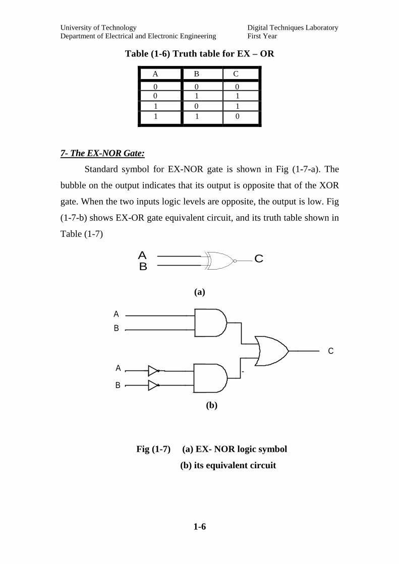
Table (1-6) Truth table for EX – OR
7- The EX-NOR Gate:
Standard symbol for EX-NOR gate is shown in Fig (1-7-a). The
bubble on the output indicates that its output is opposite that of the XOR
gate. When the two inputs logic levels are opposite, the output is low. Fig
(1-7-b) shows EX-OR gate equivalent circuit, and its truth table shown in
Table (1-7)
(a)
(b)
Fig (1-7) (a) EX- NOR logic symbol
(b) its equivalent circuit
A B C 0 0 0 0 1 1 1 0 1 1 1 0
AB
A
B
C

University of Technology Digital Techniques Laboratory Department of Electrical and Electronic Engineering First Year
1-7
Table (1-7) Truth table for EX -NOR.
When a logic gate is performing a useful function in a circuit, its
inputs can change and its output will react to these changes according to
the truth table for that gate. It is often quite useful to have a symbolic
representation for these logic states, as they change with time. A
convenient method for doing this is to draw a timing diagram. The main
purpose of a timing diagram is to show what the conditions in a logic
circuit are at any one particular time. By using timing lines, it is possible
to oversee all inputs and outputs simultaneously. If any input or output
line is displayed on an oscilloscope screen.
TIMING DIAGRAMS:
(a)
(b)
A B C
0 0 1 0 1 0 1 0 0 1 1 1
A
B
C
A
B
C

University of Technology Digital Techniques Laboratory Department of Electrical and Electronic Engineering First Year
1-8
(c)
(d)
Fig. (1-8) Timing diagram for logic gates.
(a) Timing diagram for AND gate.
(b) Timing diagram for OR gate.
(c)Timing diagram for EX-OR gate.
(d) Timing diagram for EX-NOR gate.
Boolean algebra consists of a set of laws that have logical
relationships. Unlike ordinary algebra, where an unknown can take any
value, the elements of Boolean algebra are binary variables and can have
only one of two valves 1 or 0 (also called TRUE or FALSE). Variables
are typically letters of the alphabet.
Symbols used in Boolean algebra include the bar, which is NOT or
complement, the connective + which implies logical addition and is
read " OR " and the connective which implies logical multiplication
A
B
C
A
B
C

University of Technology Digital Techniques Laboratory Department of Electrical and Electronic Engineering First Year
1-9
and is read u
AND ". The dot is frequently eliminated when logical
multiplication is shown. Thus A.B is written AB. The basic rules of
Boolean algebra are shown in Table (1-8).
Table (1-8) Basic rules of Boolean algebra
1
A + 0 =
A
2 A+ 1 =1
3 A. 0 = 0
4 A. 1 = A
5
A+ A = A
6
A+ A =1
7 A. A = A
8 A. A = 0
9 A = A
10 A + AB = A
11 A+ AB = A+B
12 (A + B)(A + C) = A + BC
Note
: -A, B, and C can represent a single variable or combination of variables

University of Technology Digital Techniques Laboratory Department of Electrical and Electronic Engineering First Year
1-10
In this experiment you will use TTL logic to become familiar with this
important family. There are several subfamilies of CMOS which have
different specifications. The original CMOS family was the 4000
series. Other families include the 54C / 74C family, which is
functionally and pin - out - compatible with TTL 54 / 74 series, and the 54
HC / 74HC, which is functionally and pin - out - compatible with TTL
54LS / 74LS logic. The 54C / 74C series is faster and can sink 50% more
current that the 4000 series. One disadvantage of CMOS is that it is
damaged more easily than TTL. Because the TTL (Transistor - Transistor
Logic) is the most widely used logic family. Almost every major
manufacturer has a TTL product line and most common TTL integrated
circuits are produced by several companies.
APPARATUS
1. Oscilloscope.
:
2. The software Electronic Work Bench
3. Function generator.
4. Logic INTIKIT unit
5. I C ‘s 7 4 0 4 , 7 4 3 2 , 7 4 0 8 , 7 4 8 6 , 7 4 0 , 7 4 0 2 , 74266.
PROCEDURE
Part One: Using practical connection:-
:
1- Connect the circuit shown in Fig. (1-1).
2- Apply a signal to (A) input from the first pulse generator of amplitude
4 V (P-P), f = 1KHz. Draw the wave form of input A.
3- Apply a signal to (B) input from the second pulse generator of
amplitude, 4V (P-P), f = 500Hz. Draw the wave from of input B.
4- Draw the output waveform of the AND logic gate.

University of Technology Digital Techniques Laboratory Department of Electrical and Electronic Engineering First Year
1-11
Vin Vout
Vin Vout
Vin Vout
5- Repeat steps (2), (3) and (4) for Fig. (1-2), Fig. (1-3), Fig. (1-4),
Fig. (1-5), Fig (1-6), Fig (1-7) and draw the output waveforms for each
figure.
6- Prove rule 1 (see Table 8) with the circuit of Fig. (1-9). Use 5V for the
power supply, with 0V to 4V level on the output. Sketch the input signal,
Vin, and voltage on your sketches. To obtain the proper time relationship
between signals, look at both signals at one time on the scope while
triggering on one channel only.
Fig. (1-9) The OR - gate that implement rule (1)
7-Change the circuit to that of Fig. (1-10). Sketch the input and output
signals.
Fig. (1-10) The OR- gate that implement rule (5).
8-Connect the circuit of Fig. (1-11). Sketch the input and output signals.
Which rule of this circuit illustrates?
Fig. (1-11) The AND - gate that implement rule (7).
9- Design a circuit that illustrates rule 10, Use the signal generator for A
and a switch (or wire) for B. Sketch the A input and output signal.

University of Technology Digital Techniques Laboratory Department of Electrical and Electronic Engineering First Year
1-12
Part Two: Simulation using Electronic Work Bench (EWB) package.
1. Connect the circuit shown in Fig. (1-1, 2, 3, 4, 5, 6, 7) by using logic
gates.
2. Connect the circuit shown in Fig. (1-1, 2, 3, 4, 5, 6, 7) by using
IC’s 7404, 7432, 7408, 7436, 7400, 7402 and 74266.
3. Repeat steps 1, 2 for three and four variables inputs and find the
truth table.
4. Connect all Boolean Algebra rules in Table (1-8) by using gates and
ICs.
The following window shows the simulation of 4-inputs OR gate using
(EWB) package.

University of Technology Digital Techniques Laboratory Department of Electrical and Electronic Engineering First Year
1-13
DISCUSSION
1- Design the logic circuit for the following conditions and draw the
output wave form, X is a 0 if any two of the three variables A, B, and
C are 1, X is a1 for all other conditions.
:
2- Implement the following function with only AND and NOT gates.
F=A B + A B + B C
W=X Y (X Z + X Y Z + Y Z) + X Z
3- TTL SSI comes mostly in 14 - pin packages. Two pins are reserved for
power supply and the other pins are used for input and output
terminals. How many gates are enclosed in one such package if it
contains the following types of gates:-
a) 2 - input exclusive - OR gates.
b) 3 - input AND gates.
c ) 4 – input NAND gates.
d) 5-input NOR gates.
e) 8 - input NAND gates.
4- Use NAND gate, NOR gate, or combinations of both to
implement the following expression:-
a) X=A [B + C (D + E)]
b) X = B (CDE + E F G) (A B + C)
5 - a) What is the applications of AND gate and OR gate?
b) In OR gate why 1 + 1 = 1?
c) The Fig. (12 - a) shows the A & B inputs and the output is C, For
the OR gate using the A and B inputs of Fig. (12 - a) draw the C
output for each of the following:
• The AND gate.
• The NAND gate Fig. (12 – b).
• The NOR gate Fig. (12 – c).
• The negative AND gate Fig. (12 – d).

University of Technology Digital Techniques Laboratory Department of Electrical and Electronic Engineering First Year
1-14
AB C A
BC
A
BC
• The negative OR gate Fig. (12 – e).
(a) (b)
(c) (d)
Fig. (1-12) For problem (5).
AB C
A B C

University of Technology Digital Techniques Laboratory Department of Electrical and Electronic Engineering First Year
2-1
EXPERIMENT NUMBER (2)
THE APPLICATIONS OF EXCLUSIVE- OR
OBJECT
The EX - OR is a widely used function because of special arithmetic
properties which will be discussed below and because of its wide
applications.
:
THEORY
1-
:
Parity Checker
Errors can occur as digital codes are being transferred from one point
to another within a digital system or while codes are being transmitted from
one system to another. The errors take the form of undesired changes in the
bits that make up the coded information that is, a 1 can change to a 0 or a
0 to 1, due to component malfunctions or electrical noise. If we have four
bit word, to detect the occurrence of an odd number of errors in this word, a
single bit will be added to the word that makes the number of (ones) in the
word either even number (even parity) or odd number (odd parity), so, if an
odd number of errors occurred in the word, then, the total number of ones
will not remain the same, it will change from odd to even or from even to
odd. The EX - OR gate is the most suitable circuit to provide parity
checker. Fig. (2-1) shown the circuit of four bit even parity checker.
:
AB
CD
X
L=even parity bitH=odd parity bit
Fig. (2-1) Four bit parity checker.

University of Technology Digital Techniques Laboratory Department of Electrical and Electronic Engineering First Year
2-2
A B C
Control signal
x y z
2- Control Inverter
The EX - OR gate can be used as a (NOT) gate by connecting one of
the inputs to logic 1, for this reason it can be used to complement a word
by using one of the inputs as control line as shown in Fig. (2-2). When
the control signal is logic zero then X=A, Y= B, Z=C, and when control
signal is logic one then X= A, Y= B, Z= C
:
Fig. (2-2) Control inverter logic circuit.
3- UBinary to Gray / Gray to Binary Conversion:
The Gray code is widely used in many digital systems specially in
shaft encoders and analog to digital converter, but it is very difficult to use
the Gray –code in arithmetic operations, since there are only one bit change
between any two consecutive Gray code number, and it is un-weighted code
and the EX-OR gate is the most suitable gate for this purpose as shown in
Fig (2-3).
(a) (b)
Fig. (2-3) (a) Gray to Binary convertor. (b) Binary to Gray convertor.
X1 X2 X3 X4
A B C D
MSB
Binary code
Gray code
X1 X2 X3 X4
A B C D
MSB
Binary code
Gray code

University of Technology Digital Techniques Laboratory Department of Electrical and Electronic Engineering First Year
2-3
The basic function of comparator is to compare the magnitude of two
quantities in order to determine the relationship of those quantities. In its
simplest form, a comparator circuit determines if two numbers are equal.
The EX-OR gate is a basic comparator because its output is a 1 if its two
input bits are not equal and a 0 if the inputs are equal. If the comparison is
such that the states of one number with respect to the other is to be specified
one of the three conditions A > B, A< B, and A = B.
4- Digital Comparator:
Table (2-1) Comparator of two numbers one bit each.
A B A>B A<B
A=B
0 0 0 0 1
1 0 1 0 0
0 1 0 1 0
1 1 0 0 1
1- Logic INTIKIT unit.
APPARATUS:
2- IC’s: 7486, 74266, 7408, 7432, 7404.
3- The software Electronic Work Bench (EWB).
University of Technology Digital Techniques Laboratory Department of Electrical and Electronic Engineering First Year
2-4
Part One: Using practical connection
PROCEDURES:
1- Connect the circuit shown in Fig. (2-1) and find the even parity bit and
add parity bit for each number.
2- Connect the circuit shown in Fig (2-2) and check the result when the
control signal is 1 and when the control signal is 0.
3- Connect 3- Bit gray to binary converter circuit and find the equivalent
binary for the following gray code numbers110, 111, 101, and 001.
Then connect 3-Bit binary to gray code converter circuit and find the
equivalent gray code for the following binary numbers 011, 000, 010,
and 111.
4-Referring to the Table (2-1) design the circuit for two bit compactor.
Part two: Using simulation Electronic Work Bench (EWB) package.
1- Connect the circuit shown in Fig. (2-1) by using logic gates and find
the even parity bit and odd parity bit for each number.
2- Connect the circuit shown in Fig (2-2) by using logic gates; check the
result when the control signal is 1 and when the control signal is 0.
3- Connect 4-Bit Gray to Binary by using logic gates, and find the truth
table.Connect 4-Bit Binary to Gray by using logic gates, and find the
truth table.
4- Connect two number comparator circuits by using logic gates.
5- Repeat steps 1, 2, 3, 4 and 5 by using IC’s.
The following window represents example of the (EWB) package.

University of Technology Digital Techniques Laboratory Department of Electrical and Electronic Engineering First Year
2-5
1- Is the Gray code arithmetic code? Why? Where this code used?
DISCUSSION:
2 - What is the parity bit?
3 - Design five - bit odd parity checker?
4- a) What are the main applications of the comparator?
b) Design two – two bit comparator.
5- Convert five bit Gray to binary code, write truth table and draw the
circuit diagram.

University of Technology Digital Techniques Laboratory Department of Electrical and Electronic Engineering First Year
3-1
EXPERIMENT NUMBER (3)
ARITHMETIC ELEMENTS
OBJECT
After completing this experiment, you will be able to design and
build any circuit that can be add and subtract binary numbers.
:
THEORY
An arithmetic element is any circuit that can add, subtract, multiply,
divide, or perform some other arithmetic function with binary numbers.
Arithmetic elements lie securely in the domain of computer technology
and the related technology of electronic calculators. With all of the
complexity of computer circuits, it is slightly reassuring to realize, that, the
basis of all the arithmetic operations that a computer performs is one simple
circuit that consist of only a few gates - the full adder. The full adder simply
adds two binary logic bits (and a carry), but as it turns out, the full adder can
be used to subtract, multiply, divide, extract square roots, and perform many
other mathematical functions.
:
1- Binary Addition
To perform the addition of two numbers in binary form, the following
four fundamental rules of algorithms are used:
:
0+0=0, 1+0=1, 0+1=1, 1+1=0 and carry 1
These algorithms can be applied to any two positive binary numbers,
(integers) and are the only basic rules that must be observed in binary
addition. For example:

University of Technology Digital Techniques Laboratory Department of Electrical and Electronic Engineering First Year
3-2
11 Carries 111
0110 6 Augend 0011 3
0011 + 3 Addend 0111 +
1001 9 Sum 1010 10
7
HALF ADDER
One logic circuit that can be used to begin implement addition
according to the above algorithms is shown in Fig. (3 - 1). It accepts two
binary digits on its input and produces two binary digits on its output, a sum
bit and a carry bit.
:
C0
S = A B
=A B
Fig. (3 - 1) Half Adder Logic Circuit
FULL ADDER
The full-adder accepts three inputs, and generates a sum output and a
carry output. It must sum the two input bits and the input carry bit, yielding
the equation for the input carry bit, yielding the equation for the sum output
of the full- adder.
:
S = (A B) Ci
The output carry is a 1 for the full-adder if both inputs to the first
exclusive –OR gate are 1s or if both inputs to the second exclusive –OR
gate are 1s.
CARRY
A B
SUM

University of Technology Digital Techniques Laboratory Department of Electrical and Electronic Engineering First Year
3-3
C0
This function is implemented and combined with the sum logic to perform a
complete full-adder circuit, as shown in Fig. (3-2). this circuit is used in
calculators, computers, and much other arithmetic circuit to perform not
only addition, but also multiplication, division, and Subtraction. All these
operations can be performed by utilizing special algorithms and the full adder
circuit.
= A B + (A B) Ci
CARRY OUT
SUM
A
B
Carry in
HA
HA
carry
sum
carrysum
Fig. (3 - 2) Full Adder Logic Circuit.
PARALLEL ADDER
The parallel adder consist of several full adder circuit stages that are inter
counted so that the carry output of one stage becomes the carry input to
the succeeding stage, as shown in Fig. (3 - 3). Therefore, a four stage parallel
adder will handle the propagation of all carries and can be used to add any
two 4 - bit binary numbers. Several significant features in parallel adder
should be understood. First, even though it is called parallel, the adder
works in a sequential manner. If we are to add the numbers:
:
1111 C (Carries)
00111 A (Augend)
01001 B (Addend)
10000 (Sum)

University of Technology Digital Techniques Laboratory Department of Electrical and Electronic Engineering First Year
3-4
A carry is generated by each stage of the addition. The first adder Uo
must complete the addition of Ao and Bo in order to generate the carry Co
input to the second stage U1.Therefore, U1 cannot correctly perform its part
of the addition sequence until Uo has completed adding and generating carry
Co. Likewise, U2 has to wait for U1 to generate carry C1 and so on. The
carries pass sequentially through all stages of the parallel adder and last sum
output is not correct until the last carry is generated. This carry propagation
is similar to propagation through the stages of a ripple counter.
Therefore, the adder in Fig. (3 - 3) is referred to as a parallel adder with
ripple carry. 'Notice that every stage of this adder performs an addition as
soon as it's A and B inputs are present, but the outputs of any stage may not
be correct until a carry input has been processed. A parallel adder with ripple
carry requires a relatively long time for all the carries to be generated and
processed.
Fulladder
U3
Fulladder
U0
Fulladder
U2
Fulladder
U1
B3 B2 B1 B0A1A2A3 A0
C3 C2 C1 C0
Sum 3 Sum 0Sum 1Sum 2Carryout
Externalcarry in
Fig. (3 - 3) Four-Bit Parallel adder.

University of Technology Digital Techniques Laboratory Department of Electrical and Electronic Engineering First Year
3-5
2-BINARY SUBTRACTION
Binary subtraction can be done in several different ways. First, to
perform direct subtraction of one binary number from another, rules or
algorithms can be written that are similar to those written for addition:
:
0 – 0 = 0, 1 – 0 = 1, 1 – 1 = 0, 0 – 1 = 1 and borrow (1)
These algorithms permit the subtraction of any two binary numbers, as
long as the minuend is larger than the subtrahend. Such subtraction is shown
by the following two examples:
1001 9 Minuend 1100 12
0101 5 Subtrahend 0011
0100 4 Difference 1001 9
3
There, is, however, another more commonly used method of subtraction,
which is based on adding the complement of one number to another
number, instead of subtracting
9 1001 Minuend 1001
-3 0011 Subtrahend 1100
6 0110 1 0101 add to the minuend
complement of subtrahend
1
0110 difference
add end-around carry to LSB
HALF and FULL SUBTRACTION
To implement the first set of subtraction algorithms above (direct
binary subtraction), a half subtractor and a full subtractor can be constructed
that correspond to the half and full adders for addition. Fig. (3 - 4) and (3-5)
show that.
:

University of Technology Digital Techniques Laboratory Department of Electrical and Electronic Engineering First Year
3-6
A
BSUM
CARRY
AB
Borrow in
Borrow out
Difference out
But just as in adder circuits, various types of gates can be used to
achieve the same result. In fact, the adder and subtractor circuits are so
similar that it is also possible to construct a combined adder / subtractor
circuit, with an ability to switch from one operation to the other by means of a
single control signal.
Fig. (3 - 4) Half subtractor Logic Circuit.
= A B Bi
= AB + (A B) Bi
Fig. (3 -5) Full Subtractor Logic Circuit.
1. Logic INTIKIT unit
APPARATUS:
2. I C’s: 7404, 7408, 7432, 7486
3. The software Electronic Work Bench (EWB).

University of Technology Digital Techniques Laboratory Department of Electrical and Electronic Engineering First Year
3-7
PROCEDURE
Part One: Practical connection.
:
1 - Connect the circuit shown in Fig. (3-1) and find its truth table.
2- Connect the circuit shown in Fig. (3 -2) and find its truth table, then find
function of its outputs.
3- Repeat step (1) for Fig. (3- 4) and, repeat step (2) for Fig. (3-5).
4- Design parallel 2 - bit adder logic circuit and find its results
Part Two: Simulation using Electronic Work Bench (EWB).
1- Connect the circuit shown in Fig. (3-1), (3-2), (3-4), (3-5) by using
logic gates.
2- Repeat step 1 using IC’s.
3- Repeat step 1 using half adder block.
4- Connect the circuits shown in Fig. (3-4), for each set of the following
binary numbers, determine the result of the following:
(a) A3 A2 A1 A0 = 0100 B3 B2 B1 B0 = 0100
(b) A3 A2 A1 A0 = 1100 B3 B2 B1 B0 = 1001
(c) A3 A2 A1 A0 = 1000 B3 B2 B1 B0 = 1011
The following window represents example of the (EWB) package.

University of Technology Digital Techniques Laboratory Department of Electrical and Electronic Engineering First Year
3-8
DISCUSSION
1 - Show that the output carry in a full adder circuit can be expressed as.
:
Ci +1 = Gi + Pi Ci = {Gi Pi + Gi Ci)
2- Using 4 Exclusive – OR gates and a 4 - bit Full adder circuit, construct a
4-bit parallel adder subtractor. Use an input select variable V so that
when V = 0,
3- Why the computers and calculators use full adder circuit and not use full
subtractor?
the circuit adds and when V = 1, the circuit subtracts.
4- What are the methods used to store the negative numbers in the
computer memory?
5- Implement half subtractor circuit using NOR gates only.
University of Technology Digital Techniques Laboratory Department of Electrical and Electronic Engineering First Year
4-1
EXPERIMENT NUMBER (4)
DECODERS AND ENCODERS
UOBJECT:
To be familiar with basics of conversion from binary to decimal by
using decoder circuits or by using encoder circuits to convert from decimal
to binary.
UTHEORY:
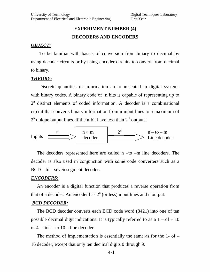
Discrete quantities of information are represented in digital systems
with binary codes. A binary code of n bits is capable of representing up to
2P
nP distinct elements of coded information. A decoder is a combinational
circuit that converts binary information from n input lines to a maximum of
2P
nP unique output lines. If the n-bit have less than 2P
nP outputs.
Inputs
The decoders represented here are called n –to –m line decoders. The
decoder is also used in conjunction with some code converters such as a
BCD – to – seven segment decoder.
UENCODERS:
An encoder is a digital function that produces a reverse operation from
that of a decoder. An encoder has 2 P
nP (or less) input lines and n output.
U BCD DECODER:
The BCD decoder converts each BCD code word (8421) into one of ten
possible decimal digit indications. It is typically referred to as a 1 – of – 10
or 4 – line – to 10 – line decoder.
The method of implementation is essentially the same as for the 1- of –
16 decoder, except that only ten decimal digits 0 through 9.
n 2n n × m decoder
n – to – m Line decoder
University of Technology Digital Techniques Laboratory Department of Electrical and Electronic Engineering First Year
4-2
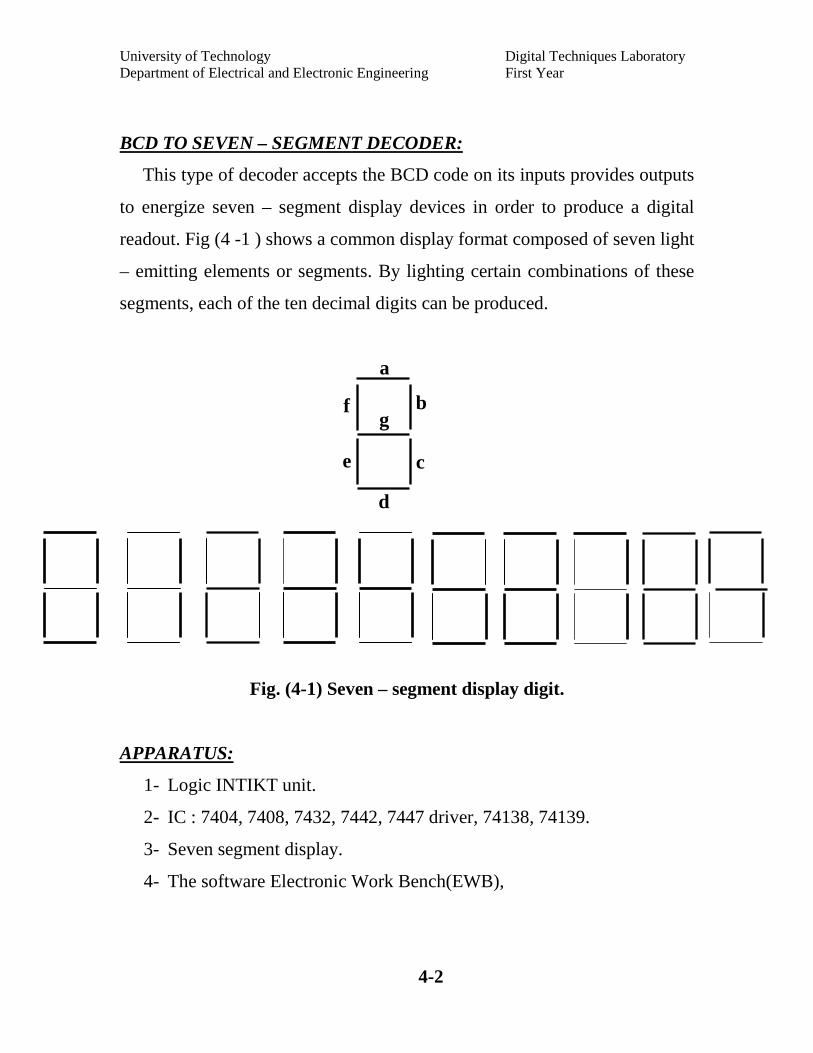
UBCD TO SEVEN – SEGMENT DECODER:
This type of decoder accepts the BCD code on its inputs provides outputs
to energize seven – segment display devices in order to produce a digital
readout. Fig (4 -1 ) shows a common display format composed of seven light
– emitting elements or segments. By lighting certain combinations of these
segments, each of the ten decimal digits can be produced.
Fig. (4-1) Seven – segment display digit.
UAPPARATUS:
1- Logic INTIKT unit.
2- IC : 7404, 7408, 7432, 7442, 7447 driver, 74138, 74139.
3- Seven segment display.
4- The software Electronic Work Bench(EWB),
a
b
f g
c
d
e

University of Technology Digital Techniques Laboratory Department of Electrical and Electronic Engineering First Year
4-3
UPROCEDURE:
Part One: Using practical connection. 1- Connect the circuit shown in Fig. (4-2) and find its truth table.
2- Connect the IC74138 (3 – to – 8 – decoder). Set data switches as
shown in 3 – to – 8 decoder truth table and record the output.
3- Connect the IC 7442 (BCD to decimal decoder). Set data switches as
shown in the BCD to decimal decoder output table, record the output
and complete the truth table.
4- Connect the circuit shown in Fig. (4-3) and find its truth table.
5- Design the circuit shown in Fig. (4-4) and produce the numbers 1,2
and 3.
Note: The IC 7447 and 74139 Active Low.
Part Two: Computer simulation using Electronic Work Bench (EWB)
package.
1. Connect the circuit shown in Fig. (4.2) using gates and ICR.
2. Connect the circuit shown in Fig. (4.2) using IC(74139).
3. Connect (3-4) decoder using IC (74139).
4. Connect the BCD to seven segment decoder using IC(7447).
Record the output and complete the truth table.
5. Connect the circuit shown in Fig.(4.3)using gates and IC, find its
truth table.

University of Technology Digital Techniques Laboratory Department of Electrical and Electronic Engineering First Year
4-4
The following window represents example of the (EWB) package.
UDISCUSSION:
1- A combinational circuit is defined by the following three functions:
Design the circuit with a decoder and external gates.
2- Design a BCD – to – excess – 3 code converter with a BCD – to –
decimal decoder and four OR gates.
3- Draw the logical diagram of a 2-line to 4 – line decoder/demultiplexer
using NOR gates only.
4- Specify the truth table of tables of an octal – to – binary priority
encoder. Provide an output to indicate if at least one of the inputs is a
1.
5- Construct a 5 × 32 decoder with four 3 × 8 decoder / demultiplexers
and 2 × 4 decoder. Use a block diagram construction.

University of Technology Digital Techniques Laboratory Department of Electrical and Electronic Engineering First Year
4-5
Table (4-1) 2 – to – 4 decoder truth table (Active High)
INPUTS OUTPUTS
B A X0 X1 X2 X3
0 0 1 0 0 0 0 1 0 1 0 0 1 0 0 0 1 0 1 1 0 0 0 1
Table (4-2) 3 – to – 8 decoder truth table(Active Low)
INPUTS OUTPUTS
C B A 0 1 2 3 4 5 6 7
0 0 0 0 1 1 1 1 1 1 1 0 0 1 1 0 1 1 1 1 1 1 0 1 0 1 1 0 1 1 1 1 1 0 1 1 1 1 1 0 1 1 1 1 1 0 0 1 1 1 1 0 1 1 1 1 0 1 1 1 1 1 1 0 1 1 1 1 0 1 1 1 1 1 1 0 1 1 1 1 1 1 1 1 1 1 1 0
B
A
X0
X1
X2
X3
Fig. (4-2) Decoder Logic Circuit (2 – to – 4 lines)

University of Technology Digital Techniques Laboratory Department of Electrical and Electronic Engineering First Year
4-6
Table (4-3) Truth table of BCD decimal decoder.
INPUTS OUTPUTS
AR3 AR2 AR1 AR0 YR0 YR1 YR2 YR3 YR4 YR5 YR6 YR7 YR8 YR9
0 0 0 0
0 0 0 1
0 0 1 0
0 0 1 1
0 1 0 0
0 1 0 1
0 1 1 0
0 1 1 1
1 0 0 0
1 0 0 1
Table (4-4) Truth table of four to two encoder.
INPUTS OUTPUTS
WR3 WR2 WR1 WR0 XR1 XR0
0 0 0 1
0 0 1 0
0 1 0 0
1 0 0 0
Fig. (4 -3) Encoder logic circuit (4- to – 2 line).
W1
W3
W2
X0
X1

University of Technology Digital Techniques Laboratory Department of Electrical and Electronic Engineering First Year
4-7
(a)
7447 BCD –to- Seven Segment Seven Segment Display
Decoder / Driver (Decimal Display)
(b)
Fig. (4 – 4) (a) Seven segment (b) BCD – to seven segment decoder.
a
b
f g
c
d
e
VCC
g f a
h
dp c
d
e
GND
+5v
1s 2s 4s 8s
BCD INPUTS
A B C D
a
b
c
d
e
f g
a
b
c
d
e
f g
Decoder 7447
GND
University of Technology Digital Techniques Laboratory Department of Electrical and Electronic Engineering First Year
5-1
EXPERIMENT NUMBER (5)
MULTIPLEXERS AND DEMULTIPLEXERS
UOBJECT:
After completing this experiment, you will be able to:-
1- Use an N – inputs multiplexer to implement, an arbitrary truth table
containing 2P
NP variables.
2- Use a demultiplexer to implement a multiplier – output combinational
circuit from the same set of input variables.
UTHEORY:
The multiplexer or data selector is a circuit that has several input lines
and a single output line. It also has control or selection inputs that permit
digital data on any one of the inputs to switched to the output line.
The circuit that performs the opposite function called demultiplexer or
decoder, which takes data from one line and distributes them to a given
number of output lines. These definitions are illustrated in Fig. (5–1). The
routing of the data is determined by additional logic signals called the select
(or address) inputs. In multiplexer IC may have an enable input to control
the operation of the unit when the enable input is in a given binary state, the
outputs are disabled, and when it is in the other state (the enable state), the
circuit function as a normal multiplexer. The enable input (sometimes called
strobe) can be used to expand two or more multiplex. Enable input digital
multiplexer with a large number of inputs. In some cases two or more
multiplexer are enclosed within one IC package.

University of Technology Digital Techniques Laboratory Department of Electrical and Electronic Engineering First Year
5-2
Fig. (5 – 1) Multiplexers and Demultiplexers.
There are many types of multiplexer such as two – to – one line
multiplexer which is shown in Fig.(5–2) and other types of MUX, 4 – to – 1
line, 8 – to – 1 line and 16 – to – 1 line multiplexer and the number of select
lines for these multiplexer are 1, 2, 3, and 4 line respectively.
The multiplexer is a very useful for connecting two or more sources to a
single, destination among computer units, and it is useful for constructing a
common bus system. One useful application for multiplexer is
implementation of combinational logic function directly.
Fig. (5 – 2) Two – to – one line MUX.
Multiplexer (Mux) Demultiplexer (Demux) Data Data in out
Switch control (select lines)
A
S
B
output

University of Technology Digital Techniques Laboratory Department of Electrical and Electronic Engineering First Year
5-3
Fig. (5 – 3) 1 – to – 2 lines DEMUX.
Boolean Function Implementation:
If we have a Boolean function of n+1 variable, we take n of these
variables and connect them to the selection lines of a multiplexer. The
remaining signal variable of the function is used for the inputs of the
multiplexer. If A is this signal able, the inputs of the multiplexer are chosen
to be either A or or 1 or 0. By judicious use of these four values for the
inputs and by connecting the other variables to the selection lines, one can
implement any Boolean function with a multiplexer. In this way it is
possible to generate any function of n+1 variable with a 2 P
nP – to – 1
multiplexer. To demonstrate this procedure with a concrete example,
consider the function of three variables:-
∑ (1, 3, 5, 6)
The function can be implemented with a 4 – to – 1 multiplexer as shown
in Fig. (5 – 4) Two of variables, B and C are applied to the selection lines in
that order. The inputs of the multiplexer are 0, 1, A, and . When BC = 00,
output F = 0. Since IR0R = 0. Therefore, both minterms mR0R = and mR4R =
produce a 0 output, since the output is 0 when BC= 00 regardless of
the value of A. when BC = 01, output F=1 since IR1R = 1 therefore, both
minterms mR1R= and mR5R = produce a 1 output, since the output is
1 when BC= 01 regardless of the value of A.
Data Input S A
B

University of Technology Digital Techniques Laboratory Department of Electrical and Electronic Engineering First Year
5-4
(a)
NUMBER A B C F
0 0 0 0 0
1 0 0 1 1
2 0 1 0 0
3 0 1 1 1
4 1 0 0 0
5 1 0 1 1
6 1 1 0 1
7 1 1 1 0
(b)
IR0 IR1 IR2 IR3
0 1 2 3
A 4 5 6 7
0 0 1 A
(c)
Fig. (5 – 4) Implementation F (A, B, C) = ∑ (1, 3, 5, 6) with multiplexer.
(a)Multiplexer – Implementation. (b) Truth table
(c)Implementation Table
0
1
A
Ā
B C
F
I0 I1 I2
4 × 1 MUX Y S1 S0

University of Technology Digital Techniques Laboratory Department of Electrical and Electronic Engineering First Year
5-5
When BC = 10, input IR2R is selected. Since A is connected to this
input, the output will be equal to 1 only for minterm but
not for minterm , because when =1 then A= 0, and since
IR2R = 0 we have F = 0. Finally when BC = 11, select IR3 R input an
connected to this input, the output will be equal 1 only for
but not forR R R.
UAPPARATUSU:
1. Logic INTIKT unit.
2. Pulse generator.
3. Oscilloscope.
4. IC 7404, 7408, 7432, 74153, 74138.
5. The software Electronic Work Bench (EWB).
UPROCEDURE:
Part One: Using practical connection. 1. Connect the circuit. Shown in Fig. (5 – 2).
2. Connect the circuit shown in Fig. (5 – 3).
3. Connect the output of Multiplexer to Demultiplexer circuit that
shown in Fig. (5 – 3) and find the output of demultiplexer when
(S= 0) and when (S = 1).
4. Connect the IC74153 (4 – to – 1 line multiplexer) set data switches
as in table (5-1) and record the output.
5. Implement the following function by using IC74153(4 – to – 1 line
multiplexer. F (A, B, C) = ∑ (2, 4, 6, 7).

University of Technology Digital Techniques Laboratory Department of Electrical and Electronic Engineering First Year
5-6
Part Two: Computer simulation using Electronic Work Bench (EWB)
package.
1. Connect the circuit shown in Fig. (5-2) gates.
2. Connect the circuit shown in Fig. (5-2) using IC (74157).
3. Connect the circuit shown in Fig. (5-3).
4. Connect the IC74153 4 to 1 multiplexer set data switches as
in table Fig. (5-4-b) and record the output.
5. Implement the following function By using IC74153
F = ABABCABC ++
Table (5-1) The 4 ×1 line multiplexer.
Select inputs Data inputs Strobe outputs
B A DR0 DR1 DR2 DR3 G Y
X X X X X X 1 0
0 0 0 X X X 0 0
0 0 1 X X X 0 1
0 1 X 0 X X 0 0
0 1 X 1 X X 0 1
1 0 X X X X 0 0
1 0 X X 0 X 0 1
1 1 X X X 0 0 0
1 1 X X X 1 0 1
Note:- X is a don’t care (0 or 1)
University of Technology Digital Techniques Laboratory Department of Electrical and Electronic Engineering First Year
5-7
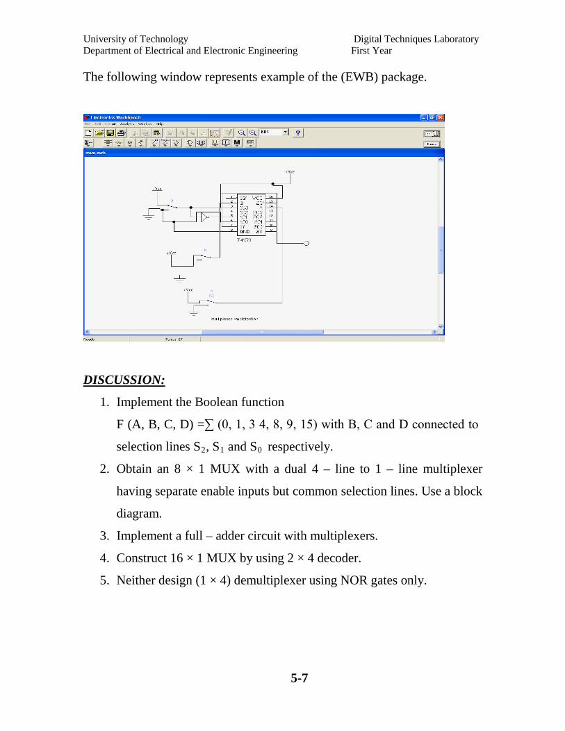
The following window represents example of the (EWB) package.
UDISCUSSION:
1. Implement the Boolean function
F (A, B, C, D) = ∑ (0, 1, 3 4, 8, 9, 15) with B, C and D connected to
selection lines SR2R, SR1R and SR0 R respectively.
2. Obtain an 8 × 1 MUX with a dual 4 – line to 1 – line multiplexer
having separate enable inputs but common selection lines. Use a block
diagram.
3. Implement a full – adder circuit with multiplexers.
4. Construct 16 × 1 MUX by using 2 × 4 decoder.
5. Neither design (1 × 4) demultiplexer using NOR gates only.

University of Technology Digital Techniques Laboratory Department of Electrical and Electronic Engineering First Year
6-1
EXPERIMENT NUMBER (6)
BISTABLE MULTIVIBRATORS (FLIP – FLOPS)
UOBJECT:
After completing this experiment, you will be able to:
1- Differentiate between various types of Flip – Flops.
2- Investigate several application circuits for both the latch and the
Flip – Flop.
UTHEORY U0TU:
Flip-Flops are synchronous bistable devices, also know as bistable
multivibratoes. This case, the term synchronous means that the output
changes state only at a specified point on a triggering input called the
clock (CLK) which is designated as a control input, C, that is, changes in
the output occur in synchronization with the clock. The most common
types of Flip-Flops are discussed below.
1- Basic Flip-Flop circuit is very important and will be analyzed in
considerable detail before proceeding to develop other circuit from
it. It is called an RS (Reset – Set) Flip-Flop or Rs latch. The latch is
type of temporary storage device that has two stable states
(bistable) and is normally placed in a category separate from that of
flip-flops. Latches are basically similar to Flip-Flops because they
are bistable devices that can reside in either of two states using a
feedback arrangement, in which the output is connected back to the
opposite inputs. To analyze the RS latch, being by raising the set
input S to logic 1 level, while holding the reset input R to logic 0,
and see what happens. First of all output goes to the logic 0 state.
But logic 0 at is connected to the lower gate and now the lower
gate has two logic 0 inputs – its output Q goes to logic 1. The logic
1 at Q is connected back to the input of the upper gate and the

University of Technology Digital Techniques Laboratory Department of Electrical and Electronic Engineering First Year
6-2
upper gate has two inputs as shown in Fig. (6 – 1) therefore, the
logic 1 at S can now become a logic 0 and the output will not
change. If the logic 1 at S goes to logic 0, the S input was used to
activate (or set) this circuit. As a result, the gates have latches
themselves in certain states, and, as long as the R input remains
logic 0, nothing will change. (Thus, this device is called a latch).
To reset the circuit, raise R to logic 1, Q will become logic 0 and
logic 1. And when S=1 the Q will be a logic 1 and when ever the R
input will be logic 1, Q=0. Finally if both inputs R and S high
simultaneously. Since any one high input to the NOR gates will
cause the output to the logic 0, both output to the logic 0, both
outputs will be logic 0 under these conditions. This special state of
the RS latch.
(a)
Input
S R
Output
Comments
0 0 NC NC No change. Latch remains in present state
0 1 0 1 Reset
1 0 1 0 Set
1 1 0 0 Not allowed
(b)
Fig. (6 -1) Latch circuit with NOR gates.
(a) Logic diagram (active high) (b) Truth table
R Q S Q
1
0 1 0

University of Technology Digital Techniques Laboratory Department of Electrical and Electronic Engineering First Year
6-3
The basic Flip – Flop circuit or RS latch can be constructed
from two NAND gates as shown in Fig. (6-2).
(a)
Input
S R
Output
Comments
0 0 N.C N.C No change. Latch remain in present state
0 1 0 1 Reset
1 0 1 0 Set
1 1 0 0 Invalid
(b)
Fig. (6 – 2) Latch circuit with NAND gates
(a) Logic diagram (active low)
(b) Truth table
1
0
1
0
S Q R Q

University of Technology Digital Techniques Laboratory Department of Electrical and Electronic Engineering First Year
6-4
2- RS FLIP – FLOP
This type of Flip – Flop constructed by adding gates to the
inputs of the basic circuit, the Flip – Flop can be made to respond
to input levels during the occurrence of clock pulse. The clocked
RS Flip – Flop shown in Fig. (6 – 3) consists of a basic NOR gate
latch and two AND gates.
The outputs of the two AND gates remain at 0 as long as the
clock pulse is 0. Regardless of the (S) and (R) input values. When
the clock pulse goes to 1, information from the (S) and (R) inputs
is allowed to reach the basic latch.
The set state is reached with S = 0, R = 1and CLK = 1. To change
to the clear state the inputs must be S = 0, R = 1 and CLK = 1.
With both S = 1 and R = 1 the occurrence of a clock pulse
causes both outputs to momentarily go to 0. When the pulse is
removed, the state of Flip – Flop is indeterminate, i.e. either state
may result, depending on whether the set or the reset input of the
latch remains a1 longer before the transition to 0 at the end of the
pulse.
(a)
Pulse Narrowing
Circuit CLK
R
S
Positive Spike
Q Q

University of Technology Digital Techniques Laboratory Department of Electrical and Electronic Engineering First Year
6-5
Inputs
S R CLK
Outputs
Comments
0 0 X No change
0 1 ↑ 0 1 RESET
1 0 ↑ 1 0 SET
1 1 ↑ ? ? Invalid
(b)
Fig. (6 – 3) S R Flip – Flop.
(a) Logic diagram. (b) Truth Table
3 – D FLIP – FLOP
The D Flip – Flop shows in Fig. (6 – 4) is a modification of R S Flip –
Flop. NAND gates 1 and 2 from a basic Flip – Flop and gates 3 and 4
modify it into a closed R S Flip – Flop. The D input goes directly to the S
input, and its complement, through gate 5, is applied to the R input. As
long as the clock pulse input is at 0 gates 3 and 4 have a 1 in their
outputs, regardless of the value of the other inputs. This conforms to the
requirement that the two inputs of a basic NAND Flip – Flop remain
initially at the 1 level. The D input is sampled during the occurrence of a
clock pulse. If it is 1, the output of gate 3 goes to 0, switching the Flip –
Flop to the set state. If it is 0, the output of gate 4 goes to 0, switching the
Flip – Flop to clear state. The D Flip – Flop receives the designation from
its ability to transfer "data" into a Flip – Flop. It is basically an R S Flip –
Flop with an inverter in the R input. The added inverter reduces the
number of inputs from two to one. This type of Flip – Flop is some times
called a gated D – latch. The CLK input is often the variable designation
to indicate that this input enables the gated latch to make possible the data
entry into to the Flip – Flop.

University of Technology Digital Techniques Laboratory Department of Electrical and Electronic Engineering First Year
6-6
(a)
(b)
Input
D CLK
Output
Comments
1 ↑ 1 0 SET (store 1)
0 ↑ 0 1 RESET (store 0)
(c)
Fig. (6 – 4) D Flip – Flop. (a) Logic diagram of D Flip – Flop
(b) Logic Symbol for D Flip-Flop (c) Truth Table
4– J – K Flip – Flop
A J – K Flip – Flop is a refinement of the RS Flip – Flop in that the
indeterminate state of the RS type is defined in the JK type. Inputs J and
K behave liked inputs S and R to set and clear the Flip – Flop (not that in
a J – K Flip – Flop. The letter J is for set and the letter K is for clear).
Pulse Narrowing
Circuit
Data D Input CK
5
3
4
1
2
Q
Q
S
R
Q
Q Data D Input
CLK

University of Technology Digital Techniques Laboratory Department of Electrical and Electronic Engineering First Year
6-7
When high are applied to both J and K simultaneously, the Flip – Flop
switches to its complement state, that is, if Q = 1, it switches to Q=0, and
vice versa. The J – K Flip – Flop shown in Fig. (6 – 5) behaves like an RS
Flip – Flop, except when both J and K are equal to 1. When both J and K
are 1, the clock pulse is transmitted through one NAND gate only, the
one whose input is connected to the Flip – Flop output which is presently
equal to 1. Thus, if Q = 1, the output of the lower NAND gate becomes 0
upon application of a clock pulse and so that the Flip – Flop will be
complement it's output.
(a)
(b)
Inputs J K CLK
Outputs
Comments
0 0 ↑ No change 0 1 ↑ 0 1 RESET 1 0 ↑ 1 0 SET 1 1 ↑ Toggle
(c)
Fig (6 – 5) J – K Flip – Flop (a) Logic diagram of J – K Flip – Flop
(b) Logic Symbol (c) Truth Table
Ǭ
Q J CLK
K Q
Q J
CLK K
Pulse Narrowing
Circuit
J
CLK
Q
Q
3
4
1
2 K

University of Technology Digital Techniques Laboratory Department of Electrical and Electronic Engineering First Year
6-8
Fig. (6 – 6) shows a J –K Flip – Flop with present and clear inputs, this
illustrates basically how these inputs are work. They can be either active
Low or active HIGH.
(a)
(b)
CLK
Pulse Narrowing
Circuit
PRE
J
K
CLR
Q
Q
Q
Q J
CLK
K
PRE
CLR

University of Technology Digital Techniques Laboratory Department of Electrical and Electronic Engineering First Year
6-9
CP CLR J K Q
X 0 1 X X ?
X 1 0 X X ?
0 1 1 X X ?
↑ 1 1 0 0 ?
↑ 1 1 0 1 ?
↑ 1 1 1 0 ?
↑ 1 1 1 0 ?
(C)
Fig. (6 – 6) J – K Flip – Flop with preset and clear.
(a) J – K Flip – Flop circuit with active LOW present and clear
(b) Logic system (C) Truth table.
5 – T Flip – Flop
The T Flip – Flop is a single – input version of the J – K Flip – Flop.
As shown in Fig. (6 – 7), the T Flip – Flop is obtained from a J – K type
if both inputs are tied together. The designation T comes from the ability
of the Flip – Flop to "toggle" or change state, it assumes the complement
state when the clock pulse occurs while input T is logic 1. The symbol
and truth table are shown in Fig. (6-7).
(a)
Q
Q T
CLK

University of Technology Digital Techniques Laboratory Department of Electrical and Electronic Engineering First Year
6-10
Inputs
T CLK
Outputs
Comments
1 ↑ Toggle
0 ↑ No change
(b)
Fig. (6 – 7) T Flip – Flop.
(a) Logic Symbol (b) Truth Table
6- Master – Slave Flip – Flop:
A master – Slave Flip – Flop is constructed from two separate Flip –
Flop. One circuit severs as a master and the other as a slave, and the
overall circuit is referred to as a master – slave Flip – Flop.
The logic diagram of a J – K master – slave Flip – Flop is shown in
Fig (6 – 8). It consists of master Flip – Flop, a slave Flip – Flop, and an
inverter. When clock pulse CLK, is 0, the output of the inverter is 1.
Since the clock input of the slave is 1, the Flip – Flop is enable and output
Q is equal to Y, while is equal to . The master Flip – Flop is disabled
because CLK = 0. When the pulse becomes 1, the information then at the
external J and K inputs is transmitted to the master Flip – Flop.
The slave Flip – Flop, however, is isolated as long as the pulse is at
its 1 level, because the output of the inverter is 0. When the pulse returns
to 0, the master flip – Flop is isolated, this prevents the external inputs
from affecting it. The slave Flip – Flop then goes to the same state as the
master Flip – Flop. The timing relationships shown in Fig. (6 – 9)
illustrate the sequence of events that occurs in master – slave Flip – Flop.

University of Technology Digital Techniques Laboratory Department of Electrical and Electronic Engineering First Year
6-11
Fig. (6 – 8) Logic diagram of master – slave Flip – Flop.
Fig. (6 – 9) Timing relation ships in a master – slave Flip – Flop
J
K
CLK
CP
J
Y Master
Q Slave
Where K = 0
Q
Q J
K Q
Q J
K
Q
Q
Y
Y Master Slave
Master – Slave Flip - Flop

University of Technology Digital Techniques Laboratory Department of Electrical and Electronic Engineering First Year
6-12
UAPPARATUS:
1- Logic INTIKT unit.
2- Oscillator.
3- Oscilloscope.
4- ICs: 7404, 7400, 7402, 7472, 7474, 7408.
5- The software Electronic Work Bench (EWB).
UPROCEDURE:
One: using practical connection.
1- Connect the circuit shown in Fig. (6 – 1 – a).
2- Apply a signal to R input from the oscillator with amplitude = 2V
(P – P), f = 500 Hz draw the wave form.
3- Apply a second signal to S input with amplitude (4V (P – P),
f=1000Hz and draw the waveform.
4- Then draw the Q output waveform.
5- Repeat step (2), (3) and (4) for Fig. (6 – 2 – a).
6- Repeat step (2), (3) and (4) for Fig. (6 – 3 – a).
7- Connect the circuit of Fig. (6 – 4 – a).
8- Apply a signal to D input from the oscillator with amplitude = 4V
(P – P), f = 50 KHz draw the waveform.
9- Apply a signal to CLK input from the clock (high speed) of the
logic INTIKT unit.
10-Draw the Q output waveform.
11- By using the IC 7474, connect the logic diagram of the D Flip –
Flop by using logic INTIKT unit and then find its truth table.
12- By using the IC 7472 connect the logic diagram of the J – K Flip
– Flop by using logic INTIKT unit and then find its truth table.
13- Connect the circuit of T Flip – Flop. Which IC will be used?
14- Connect the circuit shown in Fig. (6 – 8) and find it's output.

University of Technology Digital Techniques Laboratory Department of Electrical and Electronic Engineering First Year
6-13
Part Two: Simulation using Electronic Work Bench (EWB).
1. Connect the circuit shown in Fig. (6-1-a).
2. Connect the circuit shown in Fig. (6-2-a).
3. Connect the circuit shown in Fig. (6-3-a).
4. Connect the circuit shown in Fig. (6-4-a).
5. Repeat step 4 using Block.
6. Repeat step 4 using IC7474.
7. Connect the circuit shown in Fig. (6-5-a).
8. Repeat step 7 using Block.
9. Repeat step 7using IC7472.
The following window represents example of the (EWB) package.

University of Technology Digital Techniques Laboratory Department of Electrical and Electronic Engineering First Year
6-14
UDISCUSSION:
1- For a master – slave J – K Flip – Flop with the inputs below, sketch
the Q output waveform. Assume Q is initially low. Assume the Flip
– Flop accepts data at the positive – going edge of the clock pulse.
2- The following serial data stream is to be generated using a J – K
positive edge – triggered Flip – Flop. Determine the inputs
required. 101110010010111001000111.
3- By using J – K flip/flop from RS Flip – Flop use block diagram
and other gates.
4- The following serial data are applied to the Flip – Flop below.
Determine the resulting serial data that appear on the Q output.
There is one clock pulse for each bit time. Assume Q is initially 0.
JR1R: 1001101 KR1R: 0001110
JR2R: 0111010 KR2R:1101100
JR3R: 1111000 KR3R:1010101
5- a- what are the application of Flip – Flop. b- What is the difference
between the Flip – Flop circuit and the other combinational logic
circuits?
CK
J
K
Q
Q J
K
CK