Embed Size (px)
Citation preview

7/29/2019 DDR3 Device Operation Timing Diagram
http://slidepdf.com/reader/full/ddr3-device-operation-timing-diagram 1/154
1
DDR3+ Device Operation
DDR3+ SDRAM
Device Operation
7/29/2019 DDR3 Device Operation Timing Diagram
http://slidepdf.com/reader/full/ddr3-device-operation-timing-diagram 2/154
2
DDR3+ Device Operation
Contents
1. Functional Description1.1 Simplified State Diagram1.2 Basic Functionality1.3 RESET and Initialization Procedure
1.3.1 Power-up Initialization Sequence1.3.2 Reset Initialization with Stable Power
1.4 Register Definition1.4.1 Programming the Mode Registers1.4.2 Mode Register MR01.4.3 Mode Register MR11.4.4 Mode Register MR21.4.5 Mode Register MR3
2. DDR3 DRAM Command Description and Operation2.1 Command Truth Table2.2 CKE Truth Table2.3 No Operation (NOP) Command2.4 Deselect Command2.5 DLL-off Mode2.6 DLL on/off switching procedure
2.6.1 DLL “on” to DLL “off” Procedure2.6.2 DLL “off” to DLL “on” Procedure
2.7 Input clock frequency change2.8 Write Leveling
2.8.1 DRAM setting for write leveling & DRAM termination function in that mode2.8.2 Procedure Description2.8.3 Write Leveling Mode Exit
2.9 Extended Temperature Usage2.9.1 Auto Self-Refresh mode - ASR Mode2.9.2 Self-Refresh Temperature Range - SRT
2.10 Multi Purpose Register2.10.1 MPR Functional Description2.10.2 MPR Register Address Definition2.10.3 Relevant Timing Parameters2.10.4 Protocol Example
2.11 ACTIVE Command2.12 PRECHARGE Command2.13 READ Operation
2.13.1 READ Burst Operation2.13.2 READ Timing Definitions2.13.3 Burst Read Operation followed by a Precharge
2.14 WRITE Operation2.14.1 Burst Operation2.14.2 WRITE Timing Violations2.14.3 Write Data Mask

7/29/2019 DDR3 Device Operation Timing Diagram
http://slidepdf.com/reader/full/ddr3-device-operation-timing-diagram 3/154
3
DDR3+ Device Operation
2.14.4 tWPRE Calculation2.14.5 tWPST Calculation
2.15 Refresh Command2.16 Self-Refresh Operation2.17 Power-Down Modes
2.17.1 Power-Down Entry and Exit2.17.2 Power-Down clarifications - Case 12.17.3 Power-Down clarifications - Case 22.17.4 Power-Down clarifications - Case 3
2.18 ZQ Calibration Commands2.18.1 ZQ Calibrations Description2.18.2 ZQ Calibrations Timing2.18.3 ZQ External Resistor Value, Tolerance, and Capacitive loading
3. On-Die Termination (ODT)
3.1 ODT Mode Register and ODT Truth Table3.2 Synchronous ODT Mode3.2.1 ODT Latency and Posted ODT3.2.2 Timing Parameters3.2.3 ODT during Reads
3.3 Dynamic ODT3.3.1 Functional Description3.3.2 ODT Timing Diagrams
3.4 Asynchronous ODT Mode3.4.1 Synchronous to Asynchronous ODT Mode Transitions3.4.2 Synchronous to Asynchronous ODT Mode Transition during Power-Down Entry3.4.3 Synchronous to Asynchronous ODT Mode Transition during Power-Down Exit3.4.4 Synchronous to Asynchronous ODT Mode during short CKE high and short CKE low periods
4. AC and DC Input Measurement Levels4.1 AC and DC Logic Input Levels for Single-Ended Signals
4.1.1 AC and DC Input Levels for Single-Ended Command and Address Signals4.1.2 AC and DC Input Levels for Single-Ended Data Signals
4.2 Vref Tolerances4.3 AC and DC Logic Input Levels for Differential Signals
4.3.1 Differential signal definition4.3.2 Differential swing requirements for clock (Ck - CK) and strove (DQS - DQS)4.3.3 Single-ended requirements for differential signals
4.4 Differential Input Cross P oint Voltage4.5 Slew Rate Definitions for Single-Ended Input Signals4.6 Slew Rate Definitions for Differential Input Signals
5. AC and DC Output Measurement Levels5.1 Single Ended AC and DC Output Levels5.2 Differential AC and DC Output Levels5.3 Single Ended Output Slew Rate5.4 Differential Output Slew Rate5.5 Reference Load for AC Timing and Output Slew Rate

7/29/2019 DDR3 Device Operation Timing Diagram
http://slidepdf.com/reader/full/ddr3-device-operation-timing-diagram 4/154
4
DDR3+ Device Operation
5.6 Overshoot and Undershoot Specifications5.6.1 Address and Control Overshoot and Undershoot Specifications5.6.2 Clock, Data, Strobe and Mask Overshoot and Undershoot Specifications
5.7 Output Driver DC Electrical Characteristics5.7.1 Output Driver Temperature and Voltage sensitivity
5.8 On-Die Termination (ODT) Levels and I-V Characteristics5.8.1 On-Die Termination (ODT) Levels and I-V Characteristics5.8.2 ODT DC Electrical Characteristics5.8.3 ODT Temperature and Voltage sensitivity
5.9 ODT Timing Definitions5.9.1 Test Load for ODT Timings5.9.2 ODT Timing Definitions
6. Electrical Characteristics & AC Timing for DDR3-800 to DDR3-21336.1 Clock Specification
6.1.1 Definition for tCK (avg)6.1.2 Definition for tCK (abs)6.1.3 Definition for tCH (avg) and tCL (avg)6.1.4 Definition for tJ IT (per) and tJ IT (per, lck)6.1.5 Definition for tJ IT (cc) and tJ IT (cc, lck)6.1.6 Definition for tERR (nper)
6.2 Refresh parameters by device density
7. Electrical Characteristics and AC Timing7.1 Timing Parameters for DD3-800, DDR3-1067, DDR3-1333, and DDR3-16007.2 Timing Parameters for DDR3-1866 and DDR3-2133 Speed Bins7.3 J itter Notes
7.4 Timing Parameter Notes7.5 Address / Command Setup, Hold and Derating7.6 Data Setup, Hold and Slew Rate Derating

7/29/2019 DDR3 Device Operation Timing Diagram
http://slidepdf.com/reader/full/ddr3-device-operation-timing-diagram 5/154
5
DDR3+ Device Operation
1 . Func t iona l Desc r ip t i on
1.1 Simplified State Diagram
This simplified State Diagram is intended to provide an overview of the possible state transitions and thecommands to control them. In particular, situations involving more than one bank, the enabling or disabling of on-die termination, and some other events are not captured in full detail.
IdleZQ
Bank
Precharging
Power
Writing
ACT
READ A
READ
SRE
REF
PDE
ZQCL,ZQCS
PDX
RDX
PDE
WRITE
Automatic Sequence
Command Sequence
READ AWRITE AREAD
PRE, PREA
Refreshing
DownPowerDown
Active
READ A
WRITE A
Active Precharge
ReadingWriting
Activating
SRX
READWRITE
Calibration
PRE, PREA PRE, PREA
WRITE A
WRITE
Figure 1. Simplified State Diagram
Reading
Self Refreshing
MRS,MPR,Write
Leveling
ZQCL
InitializationResetProcedure
PowerOn
from anystate
RESET
Powerapplied
Table 1. State Diagram Command Definiti ons
Ab br eviation Fun ct ion Ab br eviati on Fun ct ion Ab br eviati on Funct ionACT Active Read RD, RDS4, RDS8 PDE Enter Power-downPRE Precharge Read A RDA, RDAS4, RDAS8 PDX Exit Power-down
PREA Precharge All Write WR, WRS4, WRS8 SRE Self-Refresh entryMRS Mode Register Set Write A WRA, WRAS4, WRAS8 SRX Self-Refresh exitREF Refresh RESET Start RESET Procedure MPR Multi-Purpose Register
ZQCL ZQ Calibration Long ZQCS ZQ Calibration Short - -Note: See “2.1 Command Truth Table” on page 22 for more details.
MRS
7/29/2019 DDR3 Device Operation Timing Diagram
http://slidepdf.com/reader/full/ddr3-device-operation-timing-diagram 6/154
6
DDR3+ Device Operation
1.2 Basic FunctionalityRead and write operation to the DDR3 SDRAM are burst oriented, start at a selected location, and continuefor a burst length of eight or a ‘chopped’ burst of four in a programmed sequence. Operation begins with theregistration of an Active command, which is then followed by a Read or Write command. The address bitsregistered coincident with the Active command are used to select the bank and row to be activated (BA0-BA2select the bank; A0-A15 select the row; refer to “DDR3 SDRAM Addressing” in each datasheet for specificrequirements). The address bits registered coincident with the Read or Write command are used to select thestarting column location for the burst operation, determine if the auto precharge command is to be issued (viaA10), and select BC4 or BL8 mode ‘on the fly’ (via A12) if enabled in the mode register.
Prior to normal operation, the DDR3 SDRAM must be powered up and initialized in a predefined manner. Thefollowing sections provide detailed information covering device reset and initialization, register definition,command descriptions, and device operation.
1.3 RESET and Init ialization Procedure
1.3.1 Power-up Initialization Sequence The following sequence is required for POWER UP and Initialization.
1. Apply power (RESET is recommended to be maintained below 0.2x VDD, (all other inputs may be unde-fined). RESET needs to be maintained for minimum 200 us with stable power. CKE is pulled “Low” any-time before RESET being de-asserted (min. time 10 ns). The power voltage ramp time between 300 mvto VDD min must be no greater than 200 ms; and during the ramp, VDD>VDDQ and (VDD-VDDQ) < 0.3volts.
- VDD and VDDQ are driven from a single power converter output, AND- The voltage levels on all pins other than VDD, VDDQ, VSS, VSSQ must be less than or equal to
VDDQ and VDD on one side and must be larger than or equal to VSSQ and VSS on the other side. Inaddition, VTT is limited to 0.95 V max once power ramp is finished, AND
- Vref tracks VDDQ/2.
OR
- Apply VDD without any slope reversal before or at the same time as VDDQ.- Apply VDDQ without any slope reversal before or at the same time as VTT & Vref.- The voltage levels on all pins other than VDD, VDDQ, VSS, VSSQ must be less than or equal to
VDDQ and VDD on one side and must be large than or equal to VSSQ and VSS on the other side.2. After RESET is de-asserted, wait for another 500 us until CKE becomes active. During this time, the
DRAM will start internal state initialization; this will be done independently of external clocks.3. Clocks (CK, CK) need to be started and stabilized for at least 10 ns or 5 tCK (which is larger) before CKE
goes active. Since CKE is a synchronous signal, the corresponding set up time to clock (tIS) must bemet. Also, a NOP or Deselect command must be registered (with tIS set up time to clock) before CKEgoes active. Once the CKE is registered “High” after Reset, CKE needs to be continuously registered“High” until the initialization sequence is finished, including expiration of tDLLK and tZQinit.
4. The DDR3 SDRAM keeps its on-die termination in high-impedance state as long as RESET is asserted.Further, the SDRAM keeps its on-die termination in high impedance state after RESET deassertion untilCKE is registered HIGH. The ODT input signal may be in undefined state until tIS before CKE is regis-tered HIGH. When CKE is registered HIGH, the ODT input signal may be statically held at either LOW orHIGH. If RTT_NOM is to be enabled in MR1, the ODT input signal must be statically held LOW. In allcases, the ODT input signal remains static until the power up initialization sequence is finished, includingthe expiration of tDLLK and tZQinit.

7/29/2019 DDR3 Device Operation Timing Diagram
http://slidepdf.com/reader/full/ddr3-device-operation-timing-diagram 7/154
7
DDR3+ Device Operation
5. After CKE is being registered high, wait minimum of Reset CKE Exit time, tXPR, before issuing the firstMRS command to load mode register. (tXPR = max (tXS; 5 x tCK)
6. Issue MRS Command to load MR2 with all application settings. (To issue MRS command for MR2, provide
“Low” to BA0 and BA2, “High” to BA1.)7. Issue MRS Command to load MR3 with all application settings. (To issue MRS command for MR3, provide“Low” to BA2, “High” to BA0 and BA1.)
8. Issue MRS Command to load MR1 with all application settings and DLL enabled. (To issue “DLL Enable”command, provide “Low” to A0, “High” to BA0 and “Low” to BA1-BA2).
9. Issue MRS Command to load MR0 with all application settings and “DLL reset” (To issue DLL reset com-mand, provide “High” to A8 and “Low” to BA0-2).
10. Issue ZQCL command to starting ZQ calibration.
11. Wait for both tDLLK and tZQinit completed.
12. The DDR3 SDRAM is now ready for normal operation.
Figure 2. Reset and Initi alization Sequence at Power-on Ramping
TaCK#
CK
Tb Tc Td Te Tf Tg Th Ti Tj Tk
MRS1) VALID1)MRS MRS ZQCLMRS
tCKSRX
NOTES:1. From time point “Td” until “Tk ” NOP or DES commands must be applied between MRS and ZQCLcommands.
TIME BREAK DON’T CARE
CKE
BA MR3 VALIDMR1 MR0MR2
VALID
T=500T=200
Tmin 10ns tIS
tXPR tMRD tMRD tMRD tMOD tZQinit
tDLLK
tIS
tIS tIS
Static LOW in case RTT_Nom is enabled at time Tg, otherwise static HIGH or LOWODT
RTT
VALID
VDD, VDDQ
Command
Reset #
7/29/2019 DDR3 Device Operation Timing Diagram
http://slidepdf.com/reader/full/ddr3-device-operation-timing-diagram 8/154
8
DDR3+ Device Operation
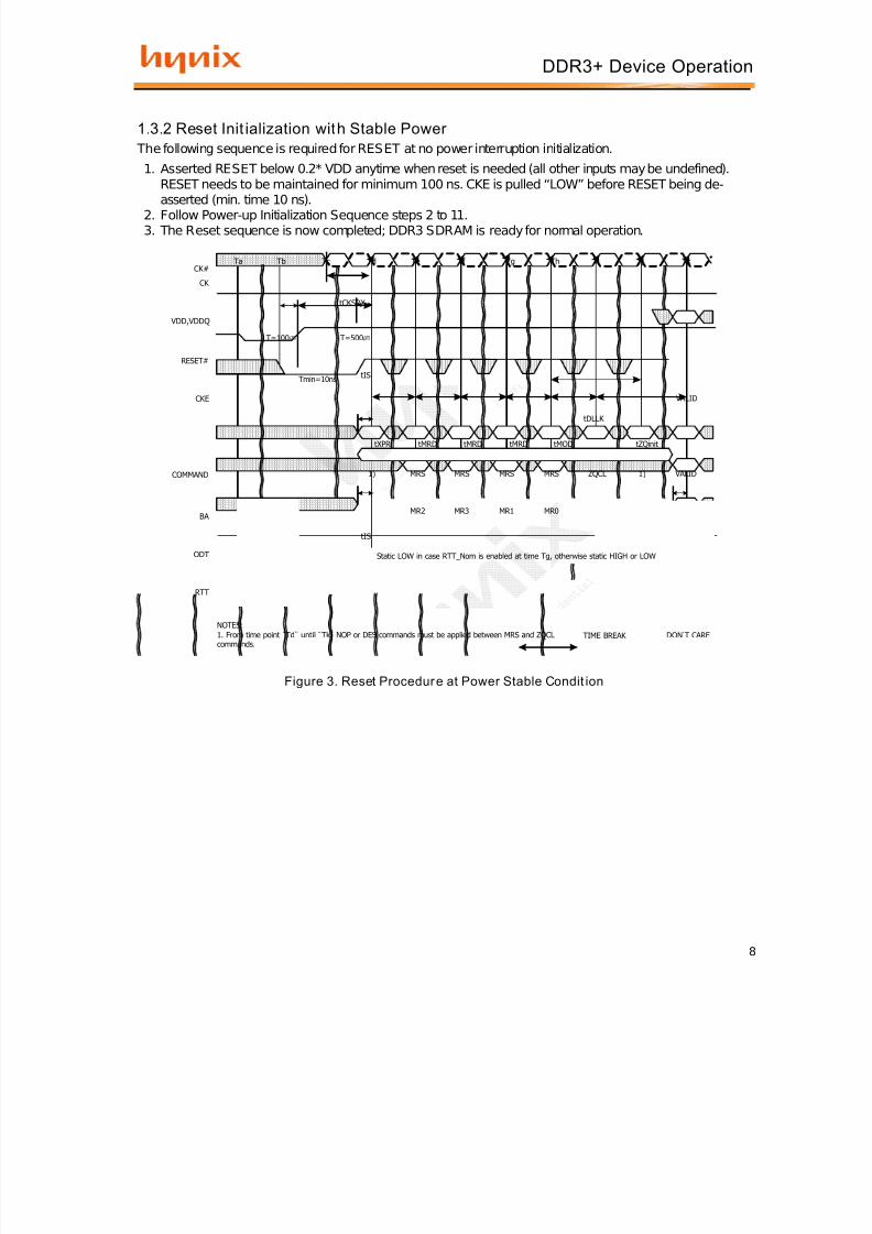
1.3.2 Reset Init ialization with Stable Power The following sequence is required for RESET at no power interruption initialization.
1. Asserted RESET below 0.2* VDD anytime when reset is needed (all other inputs may be undefined).
RESET needs to be maintained for minimum 100 ns. CKE is pulled “LOW” before RESET being de-asserted (min. time 10 ns).2. Follow Power-up Initialization Sequence steps 2 to 11.3. The Reset sequence is now completed; DDR3 SDRAM is ready for normal operation.
Figure 3. Reset Procedur e at Power Stable Condit ion
TaCK#
CK
COMMAND
Tb Tc Td Te Tf Tg Th Ti Tj Tk
MRS1) VALID1)MRS MRS ZQCLMRS
tCKSRX
NOTES:1. From time point “Td” until “Tk ” NOP or DES commands must be applied between MRS and ZQCLcommands.
TIME BREAK DON’T CARE
CKE
BA MR3 VALIDMR1 MR0MR2
VALID
T=500T=100
Tmin=10nstIS
tXPR tMRD tMRD tMRD tMOD tZQinit
tDLLK
tIS
tIS tIS
Static LOW in case RTT_Nom is enabled at time Tg, otherwise static HIGH or LOW
VDD,VDDQ
RESET#
ODT
RTT
VALID

7/29/2019 DDR3 Device Operation Timing Diagram
http://slidepdf.com/reader/full/ddr3-device-operation-timing-diagram 9/154
9
DDR3+ Device Operation
1.4 Register Definition
1.4.1 Programming the Mode Regist ers
For application flexibility, various functions, features and modes are programmable in four Mode Registers,provided by the DDR3 SDRAM, as user defined variables and they must be programmed via a Mode RegisterSet (MRS) command. As the default values of the Mode Registers (MR#) are not defined, contents of ModeRegisters must be fully initialized and/or re-initialized, i.e. written, after power-up and/or reset for proper oper-ation. Also the contents of the Mode Registers can be altered by re-executing the MRS command during nor-mal operation. When programming the mode registers, even if the user chooses to modify only a sub-set of the MRS fields, all address fields within the accessed mode register must be redefined when the MRS com-mand is issued. MRS command and DLL Reset do not affect array contents, which means these commandscan be executed any time after power-up without affecting the array contents.
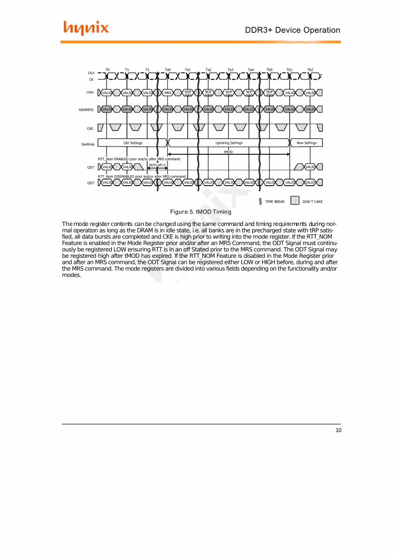
The mode register set command cycle time, tMRD is required to complete the write operation to the moderegister and is the minimum time required between two MRS commands shown in Figure 4.
Figure 4. tMRD Timing
The MRS command to Non-MRS command delay, tMOD, is required for the DRAM to update the features,except DLL reset, add is the minimum time required from an MRS command to a non-MRS command exclud-
ing NOP and DES shown in Figure 5.
ADDRESS
T0CK#
CK
T1 T2 Ta0 Ta1 Tb0 Tb1 Tb2 Tc0 Tc1 Tc2
MRS VALIDMRS VALID
Old Settings
TIME BREAK DON’T CARE
CMD
CKE
VALID
VALID VALID NOP /DES
NOP /DES
NOP /DES
NOP /DES
VALID
VALID VALID VALID VALID VALID VALID VALID VALID VALID VALID
Updating Settings New Settings
VALID VALID VALID
VALID VALID VALID VALID VALID VALID VALID VALID VALID VALID VALID
tMRD tMOD
RTT_Nom DISENABLED prior and/or after MRS command
RTT_Nom ENABLED prior and/or after MRS command
ODTLoff+1
Settings
ODT
ODT
7/29/2019 DDR3 Device Operation Timing Diagram
http://slidepdf.com/reader/full/ddr3-device-operation-timing-diagram 10/154
10
DDR3+ Device Operation
Figur e 5. tMOD Timing
The mode register contents can be changed using the same command and timing requirements during nor-mal operation as long as the DRAM is in idle state, i.e. all banks are in the precharged state with tRP satis-fied, all data bursts are completed and CKE is high prior to writing into the mode register. If the RTT_NOMFeature is enabled in the Mode Register prior and/or after an MRS Command, the ODT Signal must continu-ously be registered LOW ensuring RTT is in an off Stated prior to the MRS command. The ODT Signal may
be registered high after tMOD has expired. If the RTT_NOM Feature is disabled in the Mode Register priorand after an MRS command, the ODT Signal can be registered either LOW or HIGH before, during and afterthe MRS command. The mode registers are divided into various fields depending on the functionality and/ormodes.
T0CK#
CK
ADDRESS
T1 T2 Ta0 Ta1 Ta2 Ta3 Ta4 Tb0 Tb1 Tb2
MRS VALID VALID
Old Settings
TIME BREAK DON’T CARE
CMD
CKE
Seetings
ODT
VALID VALID NOP /DES
NOP /DES
NOP /DES
NOP /DES
VALID
Updating Settings New Settings
VALID VALID VALID
VALID VALID VALID VALID VALID VALID VALID VALID VALID VALID VALIDODT
tMOD
NOP /DES
VALID VALID VALID VALID VALID VALID VALID VALID VALID VALID VALID
ODTLoff+1
RTT_Nom DISENABLED prior and/or after MRS command
RTT_Nom ENABLED prior and/or after MRS command

7/29/2019 DDR3 Device Operation Timing Diagram
http://slidepdf.com/reader/full/ddr3-device-operation-timing-diagram 11/154
11
DDR3+ Device Operation
1.4.2 Mode Register MR0
The mode register MR0 stores the data for controlling various operating modes of DDR3 SDRAM. It controlsburst length, read burst type, CAS latency, test mode, DLL reset, WR and DLL control for precharge Power-
Down, which include various vendor specific options to make DDR3 SDRAM useful for various applications. The mode register is written by asserting low on CS, RAS, CAS, WE, BA0, BA1, and BA2, while controllingthe states of address pins according to Figure 6.
Address Field
A6 A5 A4 A2 CAS Latency
0 0 0 0 Reserved
0 0 1 0 5
0 1 0 0 6
0 1 1 0 7
1 0 0 0 81 0 1 0 9
1 1 0 0 10
1 1 1 0 11 (Optional forDDR3-1600)
A7 Mode
0 Normal
1 Test
A3 Read Bu rs t Type
0 Sequential
1 Interleave
A8 DLL Reset
0 No
1 Yes
Mode Register 0
BA1 BA0 A11 A10 A9 A8 A7 A6 A5 A4 A3 A2 A1 A0
0 TM CAS Latency RBTDLL0*1 WR
Write recovery for autoprecharge
A11 A10 A9 WR (cycl es)
0 0 0 16 *2
0 0 1 5*2
0 1 0 6*2
0 1 1 7*2
1 0 0 8*2
1 0 1 10 *2
1 1 0 12 *2
1 1 1 14 *2
A15 ~A 13
0 CL
A2 A1 BL
0 1 8 (Fixed)
0 1 BC4 of 8(on the fly)
1 0 BC4 (Fixed)
1 1 Reserved
*1: BA2 and A13~A15 are RFU and must be programmed to 0 during MRS.*2: WR (write recovery for autoprecharge) min in clock cycles is calculated by dividing tWR (in ns) by tCK (in ns) and rounding up to the nextinteger: WRmin [cycles] =Roundup (tWR [ns]/tCK [ns]). The WR value in the mode register must be programmed to be equal or larger thanWRmin. The programmed WR value is used with tRP to determine tDAL.*3: The table only shows the encodings for a given Cas Latency. For actual supported Cas Latency, please refer to speedbin tables for eachfrequency.*4: The table only shows the encodings for Write Recovery. For actual Write recovery timing, please refer to AC timingtable.
BA2
0*1
BA1 BA0 MR Select
0 0 MR0
0 1 MR1
1 0 MR2
1 1 MR3
A12
PPD
A12DLL Control for Precharge PD
0 Slow exit (DLL off)
1 Fast exit (DLL on)
Figure 6. DDR3 SDRAM mode regis ter set (MR0)
BL
A1 A0 BL
0 1 8 (Fixed)
0 1 BC4 of 8(on the fly)
1 0 BC4 (Fixed)
1 1 Reserved
7/29/2019 DDR3 Device Operation Timing Diagram
http://slidepdf.com/reader/full/ddr3-device-operation-timing-diagram 12/154
12
DDR3+ Device Operation
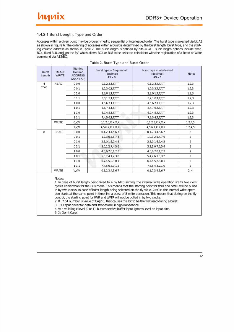
1.4.2.1 Burs t Length, Type and Order
Accesses within a given burst may be programmed to sequential or interleaved order. The burst type is selected via bit A3as shown in Figure 6. The ordering of accesses within a burst is determined by the burst length, burst type, and the start-ing column address as shown in Table 2. The burst length is defined by bits A0-A1. Burst length options include fixedBC4, fixed BL8, and ‘on the fly’ which allows BC4 or BL8 to be selected coincident with the registration of a Read or Writecommand via A12/BC.
Table 2. Burst Type and Bur st Order
BurstLength
READ/WRITE
StartingColumn
ADDRESS(A2,A1,A0)
burst type = Sequential(decimal) A3 = 0
burst type = Interleaved(decimal) A3 = 1
Notes
4Chop
READ 0 0 0 0,1,2,3,T,T,T,T 0,1,2,3,T,T,T,T 1,2,3
0 0 1 1,2,3,0,T,T,T,T 1,0,3,2,T,T,T,T 1,2,3
0 1 0 2,3,0,1,T,T,T,T 2,3,0,1,T,T,T,T 1,2,3
0 1 1 3,0,1,2,T,T,T,T 3,2,1,0,T,T,T,T 1,2,3
1 0 0 4,5,6,7,T,T,T,T 4,5,6,7,T,T,T,T 1,2,31 0 1 5,6,7,4,T,T,T,T 5,4,7,6,T,T,T,T 1,2,3
1 1 0 6,7,4,5,T,T,T,T 6,7,4,5,T,T,T,T 1,2,3
1 1 1 7,4,5,6,T,T,T,T 7,6,5,4,T,T,T,T 1,2,3
WRITE 0,V,V 0,1,2,3,X,X,X,X 0,1,2,3,X,X,X,X 1,2,4,5
1,V,V 4,5,6,7,X,X,X,X 4,5,6,7,X,X,X,X 1,2,4,5
8 READ 0 0 0 0,1,2,3,4,5,6,7 0,1,2,3,4,5,6,7 2
0 0 1 1,2,3,0,5,6,7,4 1,0,3,2,5,4,7,6 2
0 1 0 2,3,0,1,6,7,4,5 2,3,0,1,6,7,4,5 2
0 1 1 3,0,1,2,7,4,5,6 3,2,1,0,7,6,5,4 2
1 0 0 4,5,6,7,0,1,2,3 4,5,6,7,0,1,2,3 2
1 0 1 5,6,7,4,1,2,3,0 5,4,7,6,1,0,3,2 2
1 1 0 6,7,4,5,2,3,0,1 6,7,4,5,2,3,0,1 2
1 1 1 7,4,5,6,3,0,1,2 7,6,5,4,3,2,1,0 2
WRITE V,V,V 0,1,2,3,4,5,6,7 0,1,2,3,4,5,6,7 2, 4
Notes:1. In case of burst length being fixed to 4 by MR0 setting, the internal write operation starts two clockcycles earlier than for the BL8 mode. This means that the starting point for tWR and tWTR will be pulledin by two clocks. In case of burst length being selected on-the-fly via A12/BC#, the internal write opera-tion starts at the same point in time like a burst of 8 write operation. This means that during on-the-flycontrol, the starting point for tWR and tWTR will not be pulled in by two clocks.2. 0...7 bit number is value of CA[2:0] that causes this bit to be the first read during a burst.3. T: Output driver for data and strobes are in high impedance.4. V: a valid logic level (0 or 1), but respective buffer input ignores level on input pins.5. X: Don’t Care.

7/29/2019 DDR3 Device Operation Timing Diagram
http://slidepdf.com/reader/full/ddr3-device-operation-timing-diagram 13/154
13
DDR3+ Device Operation
1.4.2.2 CAS Latency
The CAS Latency is defined by MR0 (bits A9-A11) as shown in Figure 6. CAs Latency is the delay, is clock cycles,between the internal Read command and the availability of the first bit of output data. DDR3 SDRAM does not supportany half clock latencies. The overall Read Latency (RL) is defined as Additive Latency (AL) +CAS latency (CL); RL =AL+CL. For more information on the supported CL and AL settings based on the operating clock frequency, refer to “Stan-dard Speed Bins” on each datasheet. For detailed Read operation refer to “2.13 READ Operation” on page 46.
1.4.2.3 Test Mode
The normal operating mode is selected by MR0 (bit A7 =0) and all other bits set to the desired values shown in Figure 6.Programming bit A7 to a ‘1’ places the DDR3 SDRAM into a test mode that is only used by the DRAM manufacturer andshould NOT be used. No operations or functionality is specified if A7 =1.
1.4.2.4 DLL Reset
The DLL Reset bit is self-clearing, meaning that it returns back to the value of ‘0’ after the DLL reset function has beenissued. Once the DLL is enabled, a subsequent DLL Reset should be applied. Any time that the DLL reset function isused, tDLLK must be met before any functions that require the DLL can be used (i.e. Read commands or ODT synchro-nous operations).
1.4.2.5 Write Recovery
The programmed WR value MR0 (bits A9, A10, and A11) is used for the auto precharge feature along with tRP to deter-mine tDAL. WR (write recovery for auto-precharge) min in clock cycles is calculated by dividing tWR (in ns) by tCK (in ns)and rounding up to the next integer: WRmin [cycles] =Roundup (tWR [ns]/tCK [ns]). The WR must be programmed to beequal to or larger than tWR (min).
1.4.2.6 Precharge PD DLL
MR0 (bit A12) is used to select the DLL usage during precharge power-down mode. When MR0 (A12 =0), or ‘slow-exit’,the DLL is frozen after entering precharge power-down (for potential power savings) and upon exit requires tXPDLL to bemet prior to the next valid command. When MR0 (A12 =1), or ‘fast-exit’, the DLL is maintained after entering prechargepower-down and upon exiting power-down requires tXP to be met prior to the next valid command.
7/29/2019 DDR3 Device Operation Timing Diagram
http://slidepdf.com/reader/full/ddr3-device-operation-timing-diagram 14/154
14
DDR3+ Device Operation
Address Field
TDQS Mode Register 1DLL0*1 D.I.C
BA0 A15 ~ A13 A11 A10 A9 A8 A7 A6 A5 A4 A3 A2 A1 A0
A 0 DLL Enable
0 Enable1 Disable
AL
A7 Wri te l evel ing en able
0 Disabled1 Enabled
1 0*1 Rtt_Nom
Note: RZQ=240 Ω
A5 A1 Outpu t Dr iv er Im pedanc e Contr ol
0 0 RZQ/60 1 RZQ/71 0 RZQ/TBD1 1 RZQ/5
A 4 A 3 Ad di ti ve Laten cy
0 0 0 (AL disabled)0 1 CL-11 0 CL-21 1 Reserved
*1: BA2 and A8, A10, and A13~A15 are RFU and must be programmed to 0 during MRS.
BA1
0
A9 A6 A2 Rtt_Nom *3
0 0 0 Rtt_Nom disabled
0 0 1 RZQ/40 1 0 RZQ/20 1 1 RZQ/6
1 0 0 RZQ/12 *4
1 0 1 RZQ/8 *4
1 1 0 Reserved1 1 1 Reserved
A11 TDQS enable
0 Disabled1 Enabled
BA2
0*1
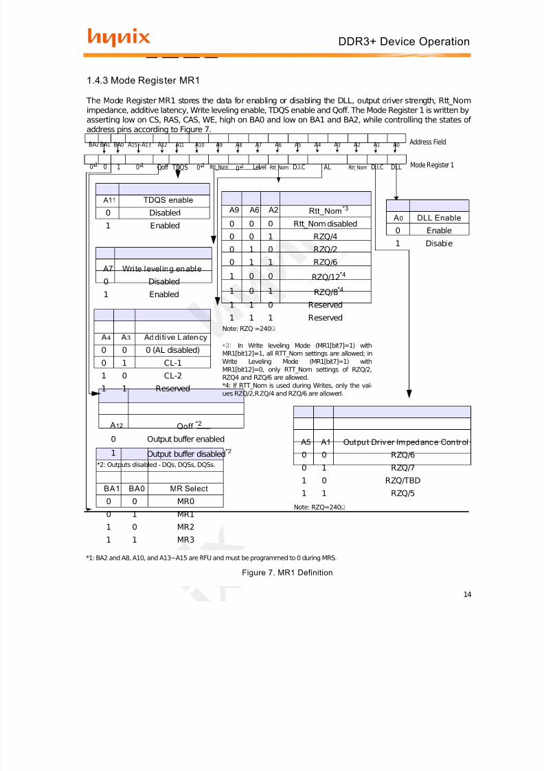
1.4.3 Mode Register MR1
The Mode Register MR1 stores the data for enabling or disabling the DLL, output driver strength, Rtt_Nomimpedance, additive latency, Write leveling enable, TDQS enable and Qoff. The Mode Register 1 is written byasserting low on CS, RAS, CAS, WE, high on BA0 and low on BA1 and BA2, while controlling the states of address pins according to Figure 7.
Qoff
A12
*2: Outputs disabled - DQs, DQSs, DQSs.
A 12 Qoff *2
0 Output buffer enabled
1 Output buffer disabled *2
Figure 7. MR1 Definition
D.I.C Rtt_NomLevel 0*1Rtt_Nom
Note: RZQ =240 Ω
*3: In Write leveling Mode (MR1[bit7]=1) with
MR1[bit12]=1, all RTT_Nom settings are allowed; inWrite Leveling Mode (MR1[bit7]=1) withMR1[bit12]=0, only RTT_Nom settings of RZQ/2,RZQ4 and RZQ/6 are allowed.*4: If RTT_Nom is used during Writes, only the val-ues RZQ/2,RZQ/4 and RZQ/6 are allowed.
BA1 BA0 MR Select
0 0 MR00 1 MR11 0 MR21 1 MR3

7/29/2019 DDR3 Device Operation Timing Diagram
http://slidepdf.com/reader/full/ddr3-device-operation-timing-diagram 15/154
15
DDR3+ Device Operation
1.4.3.1 DLL Enable/Disable
MR1 (A0=0), the DLL is automatically disabled when entering Sefl-Refresh operation and is automatically re-enabledupon eixt of Self-Refresh operation. Any time the DLL is enabled and subsequently reset, tDLLK clock cycles must occurbefore a Read or synchronous ODT command can be issued to allow time for the internal clock to be synchronized with
the external clock. Failing to wait for synchronization to occur may result in a violation of the tDQSCK, tAON or tAOFparameters. During tDLLK, CKE must continuously be registered high. DDR3 SDRAM does not require DLL for any Writeoperation, except when RTT_WR is enabled and the DLL is required for proper ODT operation. For more detailed infor-mation on DLL Disable operation refer to “2.5 DLL-off Mode” on page 27.
The direct ODT feature is not supported during DLL-off mode. The on-die termination resistors must be disabled by con-tinuously registering in the ODT pin low and/or by programming the RTT_Nom bits MR1 A9,A6,A2to 0,0,0via a moderegister set command during DLL-off mode.
The dynamic ODT feature is not supported at DLL-off mode. User must use MRS command to set Rtt_WR, MR2 A10,A9=0,0, to disable Dynamic ODT externally.
1.4.3.2 Output Driver Impedance Control
The output driver impedance of the DDR3 SDRAM device is selected by MR1 (bits A1 and A5) as shown in Figure 7.
1.4.3.3 ODT Rtt Values
DDR3 SDRAM is capable of providing two different termination values (Rtt_Nom and Rtt_WR). The nominal terminationvalue Rtt_Nom is programmed in MR1. A separate value (Rtt_WR) may be programmed in MR2 to enable a unique RTTvalue when ODT is enabled during writes. The Rtt_WR value can be applied during writes even when Rtt_Nom is dis-abled.
1.4.3.4 Addit ive Latency (AL)
Additive Latency (AL) operation is supported to make command and data bus efficient for sustainable bandwidths inDDR3 SDRAM. In this operation, the DDR3 SDRAM allows a read or write command (either with or without auto-pre-charge) to be issued immediately after the active command. The command is held for the time of the Additive Latency(AL) before it is issued inside the device. The Read Latency (RL) is controlled by the sum of the AL and CAS Latency (CL)register settings. Write Latency (WL) is controlled by the sum of the AL and CAS Write Latency (CWL) register settings. Asummary of the AL register options are shown in Table 3.
1.4.3.5 Write leveling
For better signal integrity, DDR3 memory module adopted fly-by topology for the commands, addresses, control signals,and clocks. The fly-by topology has benefits of reducing the number of stubs and their length, but it also causes flight timeskew between clock and strobe at every DRAM on the DIMM. This makes it difficult for the Controller to maintain tDQSS,tDSS, and tDSH specification. Therefore, the DDR3 SDRAM supports a ‘write leveling’ feature to allow the controller tocompensate for skew. See “2.8 Write Leveling” on page 32 for more details.
Table 3. Additi ve Latency (AL) Settings
Note : AL has a value of CL - 1 or CL - 2 as per the CL values programmed in the MR0 register
A4 A3 AL
0 1 0 (AL Disabled)0 1 CL - 11 0 CL - 21 1 Reserved

7/29/2019 DDR3 Device Operation Timing Diagram
http://slidepdf.com/reader/full/ddr3-device-operation-timing-diagram 16/154
16
DDR3+ Device Operation
1.4.3.6 Output Disable
The DDR3 SDRAM outputs may be enabled/disabled by MR1 (bit A12) as shown in Figure 7. When this feature isenabled (A12=1), all output pins (DQs, DQS, DQS, etc.) are disconnected from the device, thus removing any loading of the output drivers. This feature may be useful when measuring module power, for example. For normal operation, A12
should be set to ‘0’.
1.4.3.7 TDQS, TDQS
TDQS (Termination Data Strobe) is a feature of X8 DDR3 SDRAM that provides additional termination resistance outputsthat may be useful in some system configurations.
TDQS is not supported in X4 or X16 configurations. When enabled via the mode register, the same termination resistancefunction is applied to the TDQS/TDQS pins that is applied to the DQS/DQS pins.
In contrast to the RDQS function of DDR2 SDRAM, TDQS provides the termination resistance function only. The datastrobe function of RDQS is not provided by TDQS.
The TDQS and DM functions share the same pin. When the TDQS function is enabled via the mode register, the DMfunction is not supported. When the TDQS function is disabled, the DM function is provided and the TDQS pin is not used.See Table 4for details.
The TDQS function is available in X8 DDR3 SDRAM only and must be disabled via the mode register A11=0 in MR1 forX4 and X16 configurations.
Table 4. TDQS, TDQS Func tio n Matrix
Notes :1. If TDQS is enabled, the DM function is disabled.2. When not used, TDQS function can be disabled to save termination power.3. TDQS function is only available for X8 DRAM and must be disabled for X4 and X16.
MR1 (A11) DM/TDQS NU/TDQS
0(TDQS Disabled) DM Hi-Z1(TDQS Enabled) TDQS TDQS
7/29/2019 DDR3 Device Operation Timing Diagram
http://slidepdf.com/reader/full/ddr3-device-operation-timing-diagram 17/154
17
DDR3+ Device Operation
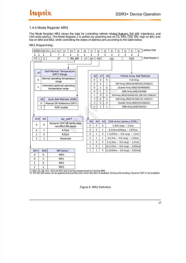
1.4.4 Mode Register MR2
The Mode Register MR2 stores the data for controlling refresh related features, Rtt_WR impedance, andCAS write latency. The Mode Register 2 is written by asserting low on CS, RAS, CAS, We, high on BA1 and
low on BA0 and BA2, while controlling the states of address pins according to the table below.MR2 Programming:
*1: BA2, A5, A8, A11~A15 are RFU and must be programmed to 0 during MRS.*2: The Rtt_WR value can be applied during writes even when Rtt_Nom is disabled. During write leveling, Dynamic ODT is not available.
Address Field
Mode Register 20*1
BA0 A15 ~ A13 A11 A10 A9 A8 A7 A6 A5 A4 A3 A2 A1 A0
0
BA1
1
BA2
0*1
A12
Rtt_WR 0*1 PASR CWL SRT ASR
BA1 BA0 MR Select
0 0 MR0
0 1 MR1
1 0 MR21 1 MR3
A2 A1 A0 Partial Array Self Refresh
0 0 0 Full Array0 0 1 Half Array (BA[2:0]=000,001,010&011)
0 1 0 Quarter Array (BA[2:0]=000&001)
0 1 1 1/8th Array (BA[2:0]=000)
1 0 0 3/4 Array (BA[2:0]=010,011,100,101,110&111)
1 0 1 Half Array (BA[2:0]=100,101,110&111)
1 1 0 Quarter Array (BA[2:0]=110&111)
1 1 1 1/8th Array (BA[2:0]=111)
A10 A9 Rtt_WR *2
0 0 Dynamic ODT off (Write doesnot affect Rtt value)
0 1 RZQ/4
1 0 RZQ/2
1 1 Reserved
A6 Auto-Self -Refresh (ASR)
0 Manual SR Reference (SRT)
1 ASR enable
Figure 8. MR2 Definition
A7Self-Refresh Temperature
(SRT) Range
0Normal operating temperature
range
1 Extended (optional) operatingtemperature range
A5 A4 A3 CAS wr ite Latency (CWL)0 0 0 5 (tCK (avg) ≥ 2.5ns)
0 0 1 6 (2.5ns>tCK(avg ≥ 1.875ns)
0 1 0 7 (1.875ns ≥ tCK (avg) ≥ 1.5ns)
0 1 1 8 (1.5ns ≥ tCK (avg) ≥ 1.25ns)
1 0 0 9 (1.25ns ≥ tCK (avg) ≥ 1.07ns)
1 0 1 10 (1.07ns ≥ tCK (avg) ≥ 0.935ns)
1 1 0 11 (0.935ns ≥ tCK (avg) ≥ 0.833ns)
7/29/2019 DDR3 Device Operation Timing Diagram
http://slidepdf.com/reader/full/ddr3-device-operation-timing-diagram 18/154
18
DDR3+ Device Operation
1.4.4.1 Partial Array Self-Refresh (PASR)
For Hynix DDR3 SDRAM If PASR (Partial Array Self-Refresh) is enabled, data located in areas of the array beyond thespecified address range shown in Figure 8 will be lost if Self-Refresh is entered. Data integrity will be maintained if tREFIconditions are met and no Self-Refresh command is issued.
1.4.4.2 CAS Write Latency (CWL)
The CAS Write Latency is defined by MR2 (bits A3-A5), as shown in Figure 8. CAS Write Latency is the delay, in clockcycles, between the internal Write command and the availability of the first bit of input data. DDR3 SDRAM does not sup-port any half-clock latencies. The overall Write Latency (WL) is defined as Additive Latency (AL) +CAS Write Latency(CWL); WL =AL +CWL. For more information on the supported CWL and AL settings based on the operating clock fre-quency, refer to “Standard Speed Bin” on each datasheet. For detailed Write operation refer to “2.14. WRITE Operation”on page 57.
1.4.4.3 Auto Self-Refresh (ASR) and Self-Refresh Temperature (SRT)
For more details refer to “2.9 Extended Temperature Usage” on page 36. Hynix DDR3 SDRAMs support Self-Refreshoperation at all supported temperatures. Applications requiring Self-Refresh operation in the Extended TemperatureRange must use the optional ASR function or program the SRT bit appropriately.
1.4.4.4 Dynamic ODT (Rtt_WR)
DDR3 SDRAM introduces a new feature “Dynamic ODT”. In certain application cases and to further enhance signal integ-rity on the data bus, it is desirable that the termination strength of the DDR3 SDRAM can be changed without issuing anMRS command. MR2 Register locations A9 and A10 configure the Dynamic ODT settings. In Write leveling mode, onlyRTT_Nom is available. For details on Dynamic ODT operation, refer to “3.3 Dynamic ODT” on page 93.

7/29/2019 DDR3 Device Operation Timing Diagram
http://slidepdf.com/reader/full/ddr3-device-operation-timing-diagram 19/154
19
DDR3+ Device Operation
1.4.5 Mode Register MR3
The Mode Register MR3 controls Multi purpose registers. The Mode Register 3 is written by asserting low onCS, RAS, CAS, WE, high on BA1 and BA0, and low on BA2 while controlling the states of address pinsaccording to the table below.
MR3 Programming:
*1: BA2, A3-A15 are RFU and must be programmed to 0 during MRS.*2: The predefined pattern will be used for read synchronization.*3: When MPR control is set for normal operation (MR3 A[2]=0) then MR3 A[1:0] will be ignored.
1.4.5.1 Mult i-Purpose Regist er (MPR)
The Multi Purpose Register (MPR) function is used to Read out a predefined system timing calibration bit sequence. Toenable the MPR, a MODE Register Set (MRS) command must be issued to MR3 Register with bit A2=1. Prior to issuingthe MRS command, all banks must be in the idle state (all banks precharged and tRP met). Once the MPR is enabled,any subsequent RD or RDA commands will be redirected to the Multi Purpose Register. When the MPR is enabled, onlyRD or RDA commands are allowed until a subsequent MRS command is issued with the MPR disabled(MR3 bit A2=0).Power-Down mode, Self-Refresh, and any other non-RD/RDA command is not allowed during MPR enable mode. TheRESET function is supported during MPR enable mode. For detailed MPR operation refer to “2.10 Multi Purpose Regis-ter” on page 38.
BA2 BA1 BA0 A15 ~ A13 A12 A11 A10 A9 A8 A7 A6 A5 A4 A3 A2 A1
0 1) 0 1 0 1) MPR 0 1) 1
A2 MPR 0 Normal operation 3)
1 Data flow from MPR
0 A0 A100
0 100 010 11
MPR Address
MPR Operation
BG0 1) EMM 0 1)
A11 BG0 Bank-Grouping disable1 Bank-Grouping enable
BG (Bank-Group)MPR location
Predefined pattern 2)
RFURFURFU
A10 ZQCS0 Normal operation1 Calibration short during Auto Ref.
Embedded mode
A0
MPR Loc
0 A11BA010
0 110 10
0 11
Bank Group ModeBank Group
Group AGroup AGroup B
Group B
0BA100001
01
0BA200000
00
BK No012
3100 110 100 11
Group AGroup BGroup B
0000101
1010101
4567
Group A
Figure 9. MR3 Definition
7/29/2019 DDR3 Device Operation Timing Diagram
http://slidepdf.com/reader/full/ddr3-device-operation-timing-diagram 20/154
20
DDR3+ Device Operation
1.4.5.2 Bank Group (BG)By using 4n prefetch scheme and also driving 8banks into 2-groups, this feature allows colum command to be issued attCCD=2nCK interval between different bank groups. A Programmable Band Group contains two Bank groups for 4n pre-fectch scheme. A bank grouping implements multiprocessing in a single physical DRAM Silicon.Bank Group (BG) Definition
[Bank Group (BG)] Burst Length and sequence
V: A valid logic level (0 or 1), but respective buffer input ignores level on input pins.X: Don’t Care.
MR3 MR0BL Note
A11 A1 A0
0 0 0 tCCD=4 CLK : BL8 (Fixed) BG Disable
0 0 1 Reserved -
0 1 0 tCCD=4 CLK : BC4 or BL8 (on the fly) BG Disable
0 1 1 Reserved -
1 0 0 tCCD=4 CLK : BL8 (Fixed) BG Enable
1 0 1tCCD=4 CLK : BL4 or BL8 (On the fly, Same bank Group)tCCD=2 CLK : BL4 (On the fly, Different bank Group)
BG Enable
1 1 0tCCD=4 CLK :BL8 (Fixed, Same bank Group)tCCD=2 CLK : BL4 (On the fly, Different bank Group) BG Enable
1 1 1 Reserved -
BurstLength
READ/WRITE
StartingColumn
ADDRESS(A2,A1,A0)
burst type = Sequential(decimal)
burst type = Interleaved(decimal)
Bank Group
8 READ
0 0 0 0, 1, 2, 3, 4, 5, 6, 7 0, 1, 2, 3, 4, 5, 6, 7
Bank Group Disableor
Enable
0 0 1 1, 2, 3, 0, 5, 6, 7, 4 1, 0, 3, 2, 5, 4, 7, 6
0 1 0 2, 3, 0, 1, 6, 7, 4, 5 2, 3, 0, 1, 6, 7, 4, 5
0 1 1 3, 0, 1, 2, 7, 4, 5, 6 3, 2, 1, 0, 7, 6, 5, 4
1 0 0 4, 5, 6, 7, 0, 1, 2, 3 4, 5, 6, 7, 0, 1, 2, 3
1 0 1 5, 6, 7, 4, 1, 2, 3, 0 5, 4, 7, 6, 1, 0, 3, 2
1 1 0 6, 7, 4, 5, 2, 3, 0, 1 6, 7, 4, 5, 2, 3, 0, 1
1 1 1 7, 4, 5, 6, 3, 0, 1, 2 7, 6, 5, 4, 3, 2, 1, 0
WRITE V V V 0, 1, 2, 3, 4, 5, 6, 7 0, 1, 2, 3, 4, 5, 6, 7
4
READ
0 0 0 0,1,2,3 0,1,2,3
Bank Group Enable
0 0 1 1,2,3,0 1,0,3,2
0 1 0 2,3,0,1 2,3,0,1
0 1 1 3,0,1,2 3,2,1,0
1 0 0 4,5,6,7 4,5,6,7
1 0 1 5,6,7,4 5,4,7,6
1 1 0 6,7,4,5 6,7,4,5
1 1 1 7,4,5,6 7,6,5,4
WRITE0 V V 0,1,2,3 0,1,2,3
1 V V 4,5,6,7 4,5,6,7

7/29/2019 DDR3 Device Operation Timing Diagram
http://slidepdf.com/reader/full/ddr3-device-operation-timing-diagram 21/154
21
DDR3+ Device Operation
[Bank Group (BG)] AC Specification for fixed BL4 / BL8
*tRRD and tFAW values depend on the size of page. Please refer to Table 41 on page 124.
1.4.5.3 Embedded Mode (ZQCS)ZQ Calibration command is used to calibrate DRAM Ron & ODT values. DDR3 SDRAM needs longer time to calibrate out-
put driver and on-die termination circuits at initialization and relatively smaller time to perform periodic calibrations.
BG disable BG enable
starting
pointSpec BG
starting
pointSpec
tWTR
Fixed BC=4 WL+2nCK 7.5ns max (4n CLK)
tWTR
Fixed BL=4same BG
WL+2nCK 7.5ns max(4n CLK)
diff. BG 3.75ns max(2n CLK)
Fixed BL=8 WL+4nCK 7.5ns max(4n CLK) Fixed BL=8same BG
WL+4nCK 7.5ns max(4n CLK)
diff. BG 3.75ns max(2n CLK)
BC=4 orBL=8 OTF
WL+4nCK 7.5ns max(4n CLK)BL=4 or
BL=8 OTFsame BG
WL+4nCK 7.5ns max(4n CLK)
diff. BG 3.75ns max(2n CLK)
BL=8 orBC=4 OTF
WL+4nCK 7.5ns max(4n CLK)BL=8 or
BL=4 OTFsame BG
WL+4nCK 7.5ns max(4n CLK)
diff. BG 3.75ns max(2n CLK)
tRTP 7.5ns (tCCD=4n CLK) tRTP 7.5ns (tCCD=4n CLK)
tRTWRL + BL/2 + 2nCLK -
WLtRTW
RL + BL/2 + 2nCLK -
WL
BG disable BG enable
tRRD
800Mbps tCCD=4nCLK 10ns max 800Mbpssame BG tCCD=4nCLK 10ns max
diff. BG tCCD=2nCLK 5ns max
1066Mbps tCCD=4nCLK 10ns max 1066Mbpssame BG tCCD=4nCLK 10ns max
diff. BG tCCD=2nCLK 5ns max
1333Mbps tCCD=4nCLK 7.5ns max 1333Mbps
same BG tCCD=4nCLK 7.5ns max
diff. BG tCCD=2nCLK 3.75ns max
1600Mbps tCCD=4nCLK 7.5ns max 1600Mbpssame BG tCCD=4nCLK 7.5ns max
diff. BG tCCD=2nCLK 3.75ns max
tFAW
800Mbps 50ns 800Mbps 50ns
1066Mbps 50ns 1066Mbps 50ns
1333Mbps 45ns 1333Mbps 45ns
1600Mbps 40ns 1600Mbps 40ns
7/29/2019 DDR3 Device Operation Timing Diagram
http://slidepdf.com/reader/full/ddr3-device-operation-timing-diagram 22/154
22
DDR3+ Device Operation
2 . DDR3 SDRAM Comm and Desc r ip t ion an d Opera t ion
2.1 Command Truth Table
(a) note 1,2,3,4 apply to the entire Command Truth Table (b) Note 5 applies to all Read/Write commands [BA = Bank Address, RA = Row Address, CA = Column Address, BC =Burst Chop, X =Don’t Care, V =Valid]
Table 5. Command Truth Table
Function Abbrevia-tion
CKE
CS RAS CAS WE BA0-BA2
A113-A15
A12-BC
A10-AP
A10-A9,A11
NotesPreviousCycle
CurrentCycle
Mode Register Set MRS H H L L L L BA OP Code
Refresh REF H H L L L H V V V V V
Self Refresh Entry SRE H L L L L H V V V V V 7,9,12
Self Refresh Exit SRX L HH X X X X X X X X 7,8,9,
12L H H H V V V V V
Single Bank Precharge PRE H H L L H L BA V V L V
Precharge all Banks PREA H H L L H L V V V H V
Bank Activate ACT H H L L H H BA Row Address (RA)
Write (Fixed BL8 orBC4) WR H H L H L L BA RFU V L CA
Write(BC4, on the Fly) WRS4 H H L H L L BA RFU L L CA
Write(BL8, on the Fly) WRS8 H H L H L L BA RFU H L CA
Write with Auto pre-charge (Fixed BL8 or
BC4)WRA H H L H L L BA RFU V H CA
1. All DDR3 SDRAM commands are defined by states of CS, RAS, CAS, WE and CKE at the rising edge of the clock. The MSB of BA,RA and CA are device density and configuration dependant.
2. RESET is Low enable command which will be used only for asynchronous reset so must be maintained HIGH during any function.3. Bank addresses (BA) determine which bank is to be operated upon. For (E)MRS BA selects an (Extended) Mode Register.4. “V” means “H or L (but a defined logic level)” and “X” means either “defined or undefined (like floating) logic level”.5. Burst reads or writes cannot be terminated or interrupted and Fixed/on-the-Fly BL will be defined by MRS.
6. The Power Down Mode does not perform any refresh operation.7. The state of ODT does not affect the states described in this table. The ODT function is not available during Self Refresh.8. Self Refresh Exit is asynchronous.9. VREF (Both VrefDQ and VrefCA) must be maintained during Self Refresh operation. VrefDQ supply may be turned OFF and
VREFDQ may take any value between VSS and VDD during Self Refresh operation, provided that VrefDQ is valid and stable priorto CKE going back High and that first Write operation or first Write Leveling Activity may not occur earlier than 512 nCK after exitfrom Self Refresh.
10. The No Operation command should be used in cases when the DDR3 SDRAM is in an idle or wait state. The purpose of the NoOperation command (NOP ) is to prevent the DDR3 SDRAM from registering any unwanted commands between operations. A NoOperation command will not terminate a previous operation that is still executing, such as a burst read or write cycle.
11. The Deselect command performs the same function as No Operation command.12. Refer to the CKE Truth Table for more detail with CKE transition.
7/29/2019 DDR3 Device Operation Timing Diagram
http://slidepdf.com/reader/full/ddr3-device-operation-timing-diagram 23/154
23
DDR3+ Device Operation
Write with Auto pre-charge (BC 4, on the
Fly)WRAS4 H H L H L L BA RFU L H CA
Write with Auto pre-charge (BL 8, on the
Fly)WRAS8 H H L H L L BA RFU H H CA
Read (Fixed BL8orBC4) RD H H L H L H BA RFU V L CA
Read(BC4, on the fly) RDS4 H H L H L H BA RFU L L CA
Read(BL8, on the fly) RDS8 H H L H L H BA RFU H L CA
Read with Auto Pre-charge (Fixed BL8 or
BC4)RDA H H L H L H BA RFU V H CA
Read with Auto Pre-charge (BC4, on the fly) RDAS4 H H L H L H BA RFU L H CA
Read with Auto Pre-charge (BL4, on the fly) RDAS8 H H L H L H BA RFU H H CA
No Operation NOP H H L H H H V V V V V 10
Device Deselected DES H H H X X X X X X X X 11
Power Down Entry PDE H LL H H H V V V V V
6,12
H X X X X X X X X
Power Down Exit PDX L HL H H H V V V V V
6,12H X X X X X X X X
ZQ Calibration Long ZQCL H H L H H L X X X H X
ZQ Calibration Short ZQCS H H L H H L X X X L X
Function Abbrevia-tion
CKE
CS RAS CAS WE BA0-BA2
A113-A15
A12-BC
A10-AP
A10-A9,A11
NotesPreviousCycle
CurrentCycle
1. All DDR3 SDRAM commands are defined by states of CS, RAS, CAS, WE and CKE at the rising edge of the clock. The MSB of BA,RA and CA are device density and configuration dependant.
2. RESET is Low enable command which will be used only for asynchronous reset so must be maintained HIGH during any function.3. Bank addresses (BA) determine which bank is to be operated upon. For (E)MRS BA selects an (Extended) Mode Register.4. “V” means “H or L (but a defined logic level)” and “X” means either “defined or undefined (like floating) logic level”.5. Burst reads or writes cannot be terminated or interrupted and Fixed/on-the-Fly BL will be defined by MRS.6. The Power Down Mode does not perform any refresh operation.7. The state of ODT does not affect the states described in this table. The ODT function is not available during Self Refresh.8. Self Refresh Exit is asynchronous.9. VREF (Both VrefDQ and VrefCA) must be maintained during Self Refresh operation. VrefDQ supply may be turned OFF and
VREFDQ may take any value between VSS and VDD during Self Refresh operation, provided that VrefDQ is valid and stable priorto CKE going back High and that first Write operation or first Write Leveling Activity may not occur earlier than 512 nCK after exitfrom Self Refresh.
10. The No Operation command should be used in cases when the DDR3 SDRAM is in an idle or wait state. The purpose of the NoOperation command (NOP ) is to prevent the DDR3 SDRAM from registering any unwanted commands between operations. A NoOperation command will not terminate a previous operation that is still executing, such as a burst read or write cycle.
11. The Deselect command performs the same function as No Operation command.12. Refer to the CKE Truth Table for more detail with CKE transition.
7/29/2019 DDR3 Device Operation Timing Diagram
http://slidepdf.com/reader/full/ddr3-device-operation-timing-diagram 24/154
24
DDR3+ Device Operation
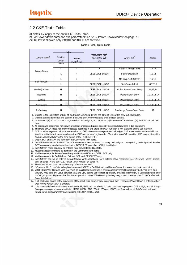
2.2 CKE Truth Table
a) Notes 1-7 apply to the entire CKE Truth Table. b) For Power-down entry and exit parameters See “2.17 Power-Down Modes” on page 79 .
c) CKE low is allowed only if tMRD and tMOD are satisfied.Table 6. CKE Truth Table
Current State 2
CKECommand (N) 3
RAS, CAS, WE,CS
Action (N) 3 NotesPreviousCycle 1
(N-1)
CurrentCycle 1 (N)
Power-DownL L X Maintain Power-Down 14,15
L H DESELECT or NOP Power-Down Exit 11,14
Self-Refresh
L L X Maintain Self-Refresh 15,16
L H DESELECT or NOP Self-Refresh Exit 8,12,16
Bank(s) Active H L DESELECT or NOP Active Power-Down Entry 11,13,14
Reading H L DESELECT or NOP Power-Down Entry 11,13,14,17
Writing H L DESELECT or NOP Power-Down Entry 11,13,14,17
Precharging H L DESELECT or NOP Power-Down Entry 11,13,14,17
Refreshing H L DESELECT or NOP Precharge Power-Down Entry 11
1. CKE(N) is the logic state of CKE at clock edge N; CKE(N-1) was the state of CKE at the previous clock edge.2. Current state is defined as the state of the DDR3 SDRAM immediately prior to clock edge N.3. COMMAND (N) is the command registered at clock edge N, and ACTION (N) is a result of COMMAND (N), ODT is not included
here.4. All states and sequences not shown are illegal or reserved unless explicitly described elsewhere in this document.5. The state of ODT does not affect the states described in this table. The ODT function is not available during Self-Refresh.6. CKE must be registered with the same value on tCKEmin consecutive positive clock edges. CKE must remain at the valid input
level the entire time it takes to achieve the tCKEmin clocks of registeration. Thus, after any CKE transition, CKE may not transitionfrom its valid level during the time period of tIS +tCKEmin +tIH.
7. DESELECT and NOP are defined in the Command Truth Table.8. On Self-Refresh Exit DESELECT or NOP commands must be issued on every clock edge occurring during the tXS period. Read or
ODT commands may be issued only after DESELECT only after tXSDLL is satisfied.9. Self-Refresh mode can only be entered from the All Banks Idle state.
10. Must be a legal command as defined in the Command Truth Table.11. Valid commands for Power-Down Entry and Exit are NOP and DESELECT only.12. Valid commands for Self-Refresh Exit are NOP and DESELECT only.13. Self-Refresh can not be entered during Read or Write operations. For a detailed list of restrictions See “2.16 Self-Refresh Opera-
tion” on page 77 and See “2.17 Power-Down Modes” on page 79 .14. The Power-Down does not perform any refresh operations.15. “X” means “don’t care” (including floating around VREF) in Self-Refresh and Power-Down. It also applies to Address pins.16. VREF (Both Vref_DQ and Vref_CA) must be maintained during Self-Refresh operaion.VrefDQ supply may be turned OFF and
VREFDQ may take any value between VSS and VDD during Self-Refresh operation, provided that VrefDQ is valid and stable priorto CKE going back High and that first Write operation or first Write Leveling Activity may not occur earlier than 512 nCK after exitfrom Self-Refresh.
17. If all banks are closed at the conclusion of the read, write or precharge command, then Precharge Power-Down is entered, other-wise Active Power-Down is entered.
18. ‘Idle state’ is defined as all banks are closed (tRP, tDAL, etc. satisfied), no data bursts are in progress, CKE is high, and all timingsfrom previous operations are satisfied (tMRD, tMOD, tRFC, tZQinit, tZQoper, tZQCS, etc.) as well as all Self-Refresh exit andPower-Down Exit parameters are satisfied (tXS, tXP, tXPDLL, etc).
7/29/2019 DDR3 Device Operation Timing Diagram
http://slidepdf.com/reader/full/ddr3-device-operation-timing-diagram 25/154
25
DDR3+ Device Operation
All Banks IdleH L DESELECT or NOP Precharge Power-Down Entry 11,13,14,18
H L REFRESH Self-Refresh 9,13,18
For more details with all signals See 2.1 “Command Truth Table” on page 20. 10
Current State 2
CKECommand (N) 3
RAS, CAS, WE,CS
Action (N) 3 NotesPrevious
Cycle 1
(N-1)
Current
Cycle 1 (N)
1. CKE(N) is the logic state of CKE at clock edge N; CKE(N-1) was the state of CKE at the previous clock edge.2. Current state is defined as the state of the DDR3 SDRAM immediately prior to clock edge N.3. COMMAND (N) is the command registered at clock edge N, and ACTION (N) is a result of COMMAND (N), ODT is not included
here.4. All states and sequences not shown are illegal or reserved unless explicitly described elsewhere in this document.5. The state of ODT does not affect the states described in this table. The ODT function is not available during Self-Refresh.6. CKE must be registered with the same value on tCKEmin consecutive positive clock edges. CKE must remain at the valid input
level the entire time it takes to achieve the tCKEmin clocks of registeration. Thus, after any CKE transition, CKE may not transitionfrom its valid level during the time period of tIS +tCKEmin +tIH.
7. DESELECT and NOP are defined in the Command Truth Table.8. On Self-Refresh Exit DESELECT or NOP commands must be issued on every clock edge occurring during the tXS period. Read or
ODT commands may be issued only after DESELECT only after tXSDLL is satisfied.9. Self-Refresh mode can only be entered from the All Banks Idle state.
10. Must be a legal command as defined in the Command Truth Table.11. Valid commands for Power-Down Entry and Exit are NOP and DESELECT only.12. Valid commands for Self-Refresh Exit are NOP and DESELECT only.13. Self-Refresh can not be entered during Read or Write operations. For a detailed list of restrictions See “2.16 Self-Refresh Opera-
tion” on page 77 and See “2.17 Power-Down Modes” on page 79.14. The Power-Down does not perform any refresh operations.15. “X” means “don’t care” (including floating around VREF) in Self-Refresh and Power-Down. It also applies to Address pins.16. VREF (Both Vref_DQ and Vref_CA) must be maintained during Self-Refresh operaion.VrefDQ supply may be turned OFF and
VREFDQ may take any value between VSS and VDD during Self-Refresh operation, provided that VrefDQ is valid and stable prior
to CKE going back High and that first Write operation or first Write Leveling Activity may not occur earlier than 512 nCK after exitfrom Self-Refresh.17. If all banks are closed at the conclusion of the read, write or precharge command, then Precharge Power-Down is entered, other-
wise Active Power-Down is entered.18. ‘Idle state’ is defined as all banks are closed (tRP, tDAL, etc. satisfied), no data bursts are in progress, CKE is high, and all timings
from previous operations are satisfied (tMRD, tMOD, tRFC, tZQinit, tZQoper, tZQCS, etc.) as well as all Self-Refresh exit andPower-Down Exit parameters are satisfied (tXS, tXP, tXPDLL, etc).

7/29/2019 DDR3 Device Operation Timing Diagram
http://slidepdf.com/reader/full/ddr3-device-operation-timing-diagram 26/154
26
DDR3+ Device Operation
2.3 No OPeration (NOP) Command
The No OPeration (NOP) command is used to instruct the selected DDR3 SDRAM to perform a NOP (CSLOW and RAS, CAS, and WE HIGH). This prevents unwanted commands from being registered during idle
or wait states. Operations already in progress are not affected.
2.4 Deselect Command
The DESELECT function (CS HIGH) prevents new commands from being executed by the DDR3 SDRAM. The DDR3 SDRAM is effectively deselected. Operations already in progress are not affected.
7/29/2019 DDR3 Device Operation Timing Diagram
http://slidepdf.com/reader/full/ddr3-device-operation-timing-diagram 27/154
27
DDR3+ Device Operation
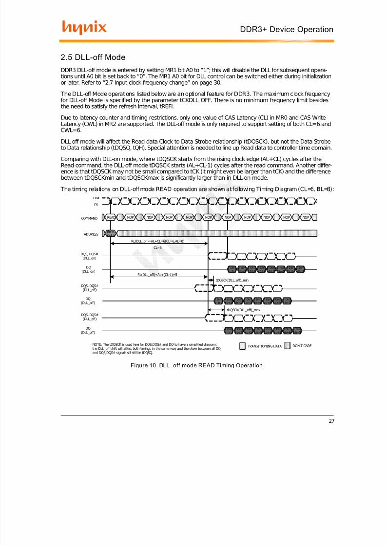
2.5 DLL-off Mode
DDR3 DLL-off mode is entered by setting MR1 bit A0 to “1”; this will disable the DLL for subsequent opera-tions until A0 bit is set back to “0”. The MR1 A0 bit for DLL control can be switched either during initialization
or later. Refer to “2.7 Input clock frequency change” on page 30. The DLL-off Mode operations listed below are an optional feature for DDR3. The maximum clock frequencyfor DLL-off Mode is specified by the parameter tCKDLL_OFF. There is no minimum frequency limit besidesthe need to satisfy the refresh interval, tREFI.
Due to latency counter and timing restrictions, only one value of CAS Latency (CL) in MR0 and CAS WriteLatency (CWL) in MR2 are supported. The DLL-off mode is only required to support setting of both CL=6 andCWL=6.
DLL-off mode will affect the Read data Clock to Data Strobe relationship (tDQSCK), but not the Data Strobeto Data relationship (tDQSQ, tQH). Special attention is needed to line up Read data to controller time domain.
Comparing with DLL-on mode, where tDQSCK starts from the rising clock edge (AL+CL) cycles after the
Read command, the DLL-off mode tDQSCK starts (AL+CL-1) cycles after the read command. Another differ-ence is that tDQSCK may not be small compared to tCK (it might even be larger than tCK) and the differencebetween tDQSCKmin and tDQSCKmax is significantly larger than in DLL-on mode.
The timing relations on DLL-off mode READ operation are shown at following Timing Diagram (CL=6, BL=8):
Figure 10. DLL_off mode READ Timing Operation
NOTE: The tDQSCK is used fere for DQS,DQS# and DQ to have a simplified diagram;the DLL_off shift will affect both timings in the same way and the skew between all DQand DQS,DQS# signals sill still be tDQSQ.
CK#
CK
COMMAND
ADDRESS
DQS, DQS#(DLL_on)
NOPNOP NOP NOP NOPNOPNOP NOP NOP
DQ(DLL_on)
Dinb
TRANSITIONING DATA DON’T CARE
READ NOP
Bank.Col b
Dinb+2
Dinb+3
RL(DLL_on)=AL+CL=6(CL=6,AL=0)
Dinb+4
Dinb+6
Dinb+7
Dinb
Dinb+2
Dinb+3
Dinb+4
Dinb+6
Dinb+7
Dinb
Dinb+2
Dinb+3
Dinb+4
Dinb+6
Dinb+7
CL=6
RL(DLL_off)=AL+(CL-1)=5
tDQSCK(DLL_off)_min
tDQSCK(DLL_off)_max
DQS, DQS#(DLL_off)
DQS, DQS#(DLL_off)
DQ(DLL_off)
DQ(DLL_off)
Dinb+2
Dinb+5
Dinb+2
Dinb+5
Dinb+2
Dinb+5

7/29/2019 DDR3 Device Operation Timing Diagram
http://slidepdf.com/reader/full/ddr3-device-operation-timing-diagram 28/154
28
DDR3+ Device Operation
2.6 DLL on/off switching procedure
DDR3 DLL-off mode is entered by setting MR1 bit A0 to “1”; this will disable the DLL for subsequent opera-tions until A0 bit is set back to “0”.
2.6.1 DLL “ on” to DLL “ off” Procedure
To switch from DLL “on” to DLL “off” requires the frequency to be changed during Self-Refresh, as outlined inthe following procedure:
1. Starting from Idle state (All banks pre-charged, all timings fulfilled, and DRAMs On-die Terminationresistors, RTT, must be in high impedance state before MRS to MR1 to disable the DLL).
2. Set MR1 bit A0 to “1” to disable the DLL.3. Wait tMOD.4. Enter Self Refresh Mode; wait until (tCKSRE) is satisfied.5. Change frequency, in guidance with “2.7 Input clock frequency change” on page 30 .6. Wait until a stable clock is available for at least (tCKSRX) at DRAM inputs.7. Starting with the Self Refresh Exit command, CKE must continuously be registered HIGH until all
tMOD timings from any MRS command are satisfied. In addition, if any ODT features were enabled inthe mode registers when Self Refresh mode was entered, the ODT signal must continuously be reg-istered LOW until all tMOD timings from any MRS command are satisfied. If both ODT features weredisabled in the mode registers when Self Refresh mode was entered, ODT signal can be registeredLOW or HIGH.
8. Wait tXS, then set Mode Registers with appropriate values (especially an update of CL, CWL andWR may be necessary. A ZQCL command may also be issued after tXS).
9. Wait for tMOD, then DRAM is ready for next command.
Figure 11. DLL Switch Sequence fro m DLL-on to DLL-off
T0CK#
CK
T1 Ta0 Ta1 Tb0 Tc0 Td0 Td1 Te0 Te1 Tf0
NOP SRE(3) NOP VALID(8)SRX(6) NOP MRS(7)MRS(2)
ODT
tMOD
NOTES:1. Starting with Idle State, RTT in Hi-Z state2. Disable DLL by setting MR1 Bit A0 to 13. Enter SR 4. Change Frequency5. Clock must be stable tCKSRX6. Exit SR 7. Update Mode registers with DLL off parameters setting8. Any valid command
TIME BREAK DON’T CARE
CMD
ODT: Static LOW in case RTT_WR is enabled, otherwise static Low or High
VALID(8)
VALID(8)
tCKSRE tCKSRX(5) tXS tMOD(4)
tCKESR
CKE
(1)
NOP

7/29/2019 DDR3 Device Operation Timing Diagram
http://slidepdf.com/reader/full/ddr3-device-operation-timing-diagram 29/154
29
DDR3+ Device Operation
2.6.2 DLL “ off” to DLL “ on” Procedure
To switch from DLL “off” to DLL “on” (with required the frequency change) during Self-Refresh:
1. Starting from Idle state (All banks pre-charged, all timings fulfilled, and DRAMs On-die Terminationresistors (RTT) must be in high impedance state before Self-Refresh mode is entered.)
2. Enter Self Refresh Mode, wait until tCKSRE satisfied.3. Change frequency, in guidance with “2.7 Input clock frequency change” on page 30 .4. Wait until a stable clock is available for at least (tCKSRX) at DRAM inputs.5. Starting with the Self Refresh Exit command, CKE must continuously be registered HIGH until tDLLK
timing from subsequent DLL Reset command is satisfied. In addition, if any ODT features wereenabled in the mode registers when Self Refresh mode was entered, the ODT signal must continu-ously be registered LOW until tDLLK timings from subsequent DLL Reset command is satisfied. If both ODT features are disabled in the mode registers when Self Refresh mode was entered, ODTsignal can be registered LOW or HIGH.
6. Wait tXS, then set MR1 bit A0 to “0” to enable the DLL.7. Wait tMRD, then set MR1 bit A8 to “1” to start DLL Reset.8. Wait tMRD, then set Mode Registers with appropriate values (especially an update of CL, CWL and
WR may be necessary. After tMOD satisfied from any proceeding MRS command, may also beissued during or after tDLLK.)
9. Wait for tMOD, then DRAM is ready for next command (Remember to wait tDLLK after DLL Resetbefore applying command requiring a locked DLL!). In addition, wait also for tZQoper in case a ZQCLcommand was issued.
Figure 12. DLL Switch Sequence from DLL Off to DLL On
T0CK#
CK
Ta0 Ta1 Tb0 Tc0 Tc1 Td0 Te0 Tf1 Tg0 Th0
SRE(2) NOP VALID(9)SRX(5) MRS(6) MRS(7)NOP
ODT
tMOD
NOTES:1. Starting with Idle State2. Enter SR 3. Change Frequency4. Clock must be stable tCKSRX5. Exit SR 6. Set DLL on by MR1 A0=07. Update Mode registers8. Any valid command
TIME BREAK DON’T CARE
CMD
ODT: Static LOW in case RTT_WR is enabled, otherwise static Low or High
VALID
(3) tXS tMRD tMRDtCKSRX(4)
tCKESR
CKE
(1)
MRS(8)
ODTLoff+1xtCK
tDLLK
7/29/2019 DDR3 Device Operation Timing Diagram
http://slidepdf.com/reader/full/ddr3-device-operation-timing-diagram 30/154
30
DDR3+ Device Operation
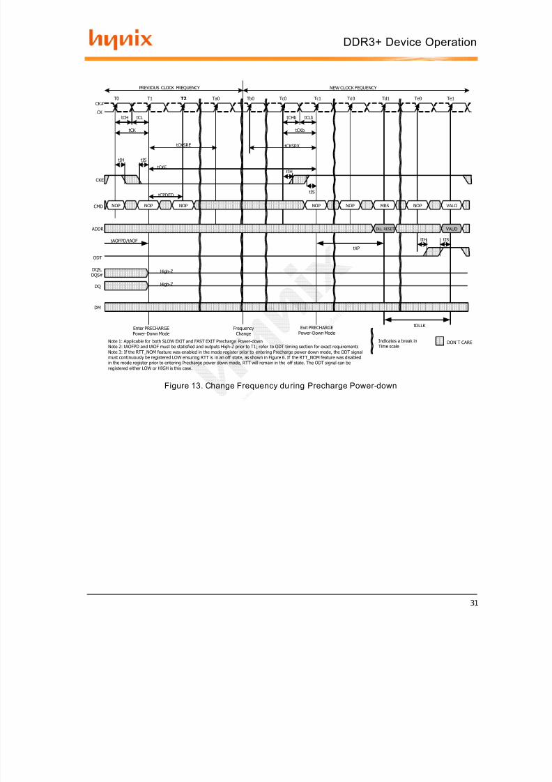
2.7 Input clock frequency change
Once the DDR3 SDRAM is initialized, the DDR3 SDRAM requires the clock to be “stable” during almost allstates of normal operation. This means once the clock frequency has been set and is to be in the “stable
state”, the clock period is not allowed to deviate except for what is allowed for by the clock jitter and SSC(spread spectrum clocking) specifications.
The input clock frequency can be changed from one stable clock rate to another stable clock rate under twoconditions: (1) Self-Refresh mod and (2) precharge Power-down mode. Outside of these two modes, it is ille-gal to change the clock frequency.
For the first condition, once the DDR3 SDRAM has been successfully placed in to Self-Refresh mode andtCKSRE has been satisfied, the state of the clock becomes a don’t care. Once a don’t care, changing theclock frequency is permissible, provided the new clock frequency is stable prior to tCKSRX. When enteringand exiting Self-Refresh mode for the sole purpose of changing the clock frequency, the Self-Refresh entryand exit specifications must still be met as outlined in See “2.16 Self-Refresh Operation” on page 77 . TheDDR3 SDRAM input clock frequency is allowed to change only within the minimum and maximum operatingfrequency specified for the particular speed grade. Any frequency change below the minimum operating fre-
quency would require the use of DLL_on-mode->DLL_off-mode transition sequence, refer to “2.6 DLL on/off switching procedure” on page 28.
The second condition is when the DDR3 SDRAM is in Precharge Power-down mode (either fast exit mode orslow exit mode). If the RTT_NOM feature was enabled in the mode register prior to entering Precharge powerdown mode, the ODT signal must continuously be registered LOW ensuring RTT is in an off state. If theRTT_NOM feature was disabled in the mode register prior to entering Precharge power down mode, RTT willremain in the off state. The ODT signal can be registered either LOW or HIGH in this case. A minimum of tCK-SRE must occur after CKE goes LOW before the clock frequency may change. The DDR3 SDRAM inputclock frequency is allowed to change only within the minimum and maximum operating frequency specifiedfor the particular speed grade. During the input clock frequency change, ODT and CKE must be held at stableLOW levels. Once the input clock frequency is changed, stable new clocks must be provided to the DRAMtCKSRX before Precharge Power-down may be exited; after Precharge Power-down is exited and tXP hasexpired, the DLL must be RESET via MRS. Depending on the new clock frequency additional MRS com-mands may need to be issued to appropriately set the WR, CL, and CWL with CKE continuously registeredhigh. During DLL re-lock period, ODT must remain LOW and CKE must remain HIGH. After the DLL locktime, the DRAM is ready to operate with new clock frequency. This process is depicted in Figure 13 on page31 .
7/29/2019 DDR3 Device Operation Timing Diagram
http://slidepdf.com/reader/full/ddr3-device-operation-timing-diagram 31/154
31
DDR3+ Device Operation
T0 T1 Tc0T2 Ta0 Tb0 Tc1 Td0 Td1 Te0 Te1
PREVIOUS CLOCK FREQUENCY NEW CLOCK FEQUENCY
tCH tCL
tCK
tCKSRE
tCHb tCLb
tCKb
tCKSRX
tCKE
tIStIH
tIS
tIH
NOP NOPNOP NOP NOP MRS NOP VALO
DLL RESET VAUD
tIH tIStAOFPD/tAOFtXP
High-Z
High-Z
CK#
CK
CKE
ADDR
ODT
DQ
DM
Enter PRECHARGEPower-Down Mode
FrequencyChange
Exit PRECHARGEPower-Down Mode
tDLLK
Indlcates a break inTime scale
DON’T CARENote 1: Applicable for both SLOW EXIT and FAST EXIT Precharge Power-downNote 2: tAOFPD and tAOF must be statisfied and outputs High-Z prior to T1; refer to ODT timing section for exact requirementsNote 3: If the RTT_NOM feature was enabled in the mode register prior to entering Precharge power down mode, the ODT signalmust continuously be registered LOW ensuring RTT is in an off state, as shown in Figure 6. If the RTT_NOM feature was disabledin the mode register prior to entering Precharge power down mode, RTT will remain in the off state. The ODT signal can beregistered either LOW or HIGH is this case.
tCPDED
CMD
DQS,DQS#
Figure 13. Change Frequency du ring Precharge Power-down
7/29/2019 DDR3 Device Operation Timing Diagram
http://slidepdf.com/reader/full/ddr3-device-operation-timing-diagram 32/154
32
DDR3+ Device Operation
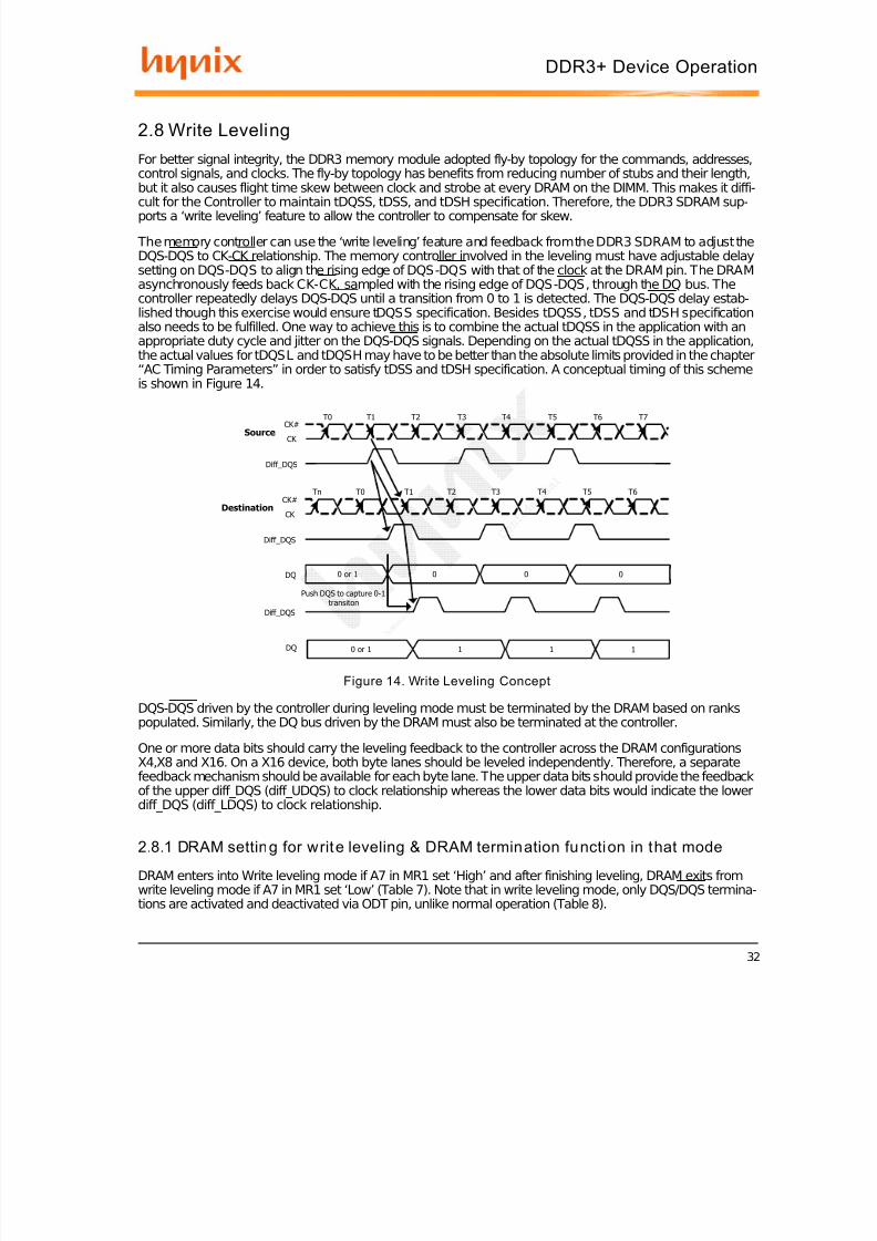
2.8 Write Leveling
For better signal integrity, the DDR3 memory module adopted fly-by topology for the commands, addresses,control signals, and clocks. The fly-by topology has benefits from reducing number of stubs and their length,
but it also causes flight time skew between clock and strobe at every DRAM on the DIMM. This makes it diffi-cult for the Controller to maintain tDQSS, tDSS, and tDSH specification. Therefore, the DDR3 SDRAM sup-ports a ‘write leveling’ feature to allow the controller to compensate for skew.
The memory controller can use the ‘write leveling’ feature and feedback from the DDR3 SDRAM to adjust theDQS-DQS to CK-CK relationship. The memory controller involved in the leveling must have adjustable delaysetting on DQS-DQS to align the rising edge of DQS-DQS with that of the clock at the DRAM pin. The DRAMasynchronously feeds back CK-CK, sampled with the rising edge of DQS-DQS, through the DQ bus. Thecontroller repeatedly delays DQS-DQS until a transition from 0 to 1 is detected. The DQS-DQS delay estab-lished though this exercise would ensure tDQSS specification. Besides tDQSS, tDSS and tDSH specificationalso needs to be fulfilled. One way to achieve this is to combine the actual tDQSS in the application with anappropriate duty cycle and jitter on the DQS-DQS signals. Depending on the actual tDQSS in the application,the actual values for tDQSL and tDQSH may have to be better than the absolute limits provided in the chapter“AC Timing Parameters” in order to satisfy tDSS and tDSH specification. A conceptual timing of this schemeis shown in Figure 14.
Figure 14. Write Leveling Concept
DQS-DQS driven by the controller during leveling mode must be terminated by the DRAM based on rankspopulated. Similarly, the DQ bus driven by the DRAM must also be terminated at the controller.
One or more data bits should carry the leveling feedback to the controller across the DRAM configurations
X4,X8 and X16. On a X16 device, both byte lanes should be leveled independently. Therefore, a separatefeedback mechanism should be available for each byte lane. The upper data bits should provide the feedbackof the upper diff_DQS (diff_UDQS) to clock relationship whereas the lower data bits would indicate the lowerdiff_DQS (diff_LDQS) to clock relationship.
2.8.1 DRAM setting for writ e leveling & DRAM termination function in that mode
DRAM enters into Write leveling mode if A7 in MR1 set ‘High’ and after finishing leveling, DRAM exits fromwrite leveling mode if A7 in MR1 set ‘Low’ (Table 7). Note that in write leveling mode, only DQS/DQS termina-tions are activated and deactivated via ODT pin, unlike normal operation (Table 8).
T0CK#
CK
DQ
T1 T2 T3 T4 T5 T6 T7
Diff_DQS
Push DQS to capture 0-1transiton
Tn T0 T1 T2 T3 T4 T5 T6
0 or 1 0 0 0
0 or 1 1 1 1
Source
CK#
CK
Diff_DQS
Destination
DQ
Diff_DQS

7/29/2019 DDR3 Device Operation Timing Diagram
http://slidepdf.com/reader/full/ddr3-device-operation-timing-diagram 33/154
33
DDR3+ Device Operation
2.8.2 Procedure Descrip tion
Memory controller initiates Leveling mode of all DRAMs by setting bit 7 of MR1 to 1. With entering write level-ing mode, the DQ pins are in underfined driving mode. During white leveling mode, only NOP or DESELECTcommands are allowed, as well as an MRS command to change Qoff bit (MR1[A12]) and an MRS commandto exit (MR1[A7]). Upon exiting write leveling mode, the MRS command performing the exit (MR7[A7]=0) mayalso change MR1 bits of A12-A11, A9, A6-A5, and A2-A1. Since the controller levels one rank at a time, theoutput of other ranks must be disabled by setting MR1 bit A12 to 1. Controller may assert ODT after tMOD,time at which time the DRAM is ready to accept the ODT signal.
The Controller may drive DQS low and DQS high after a delay of tWLDQSEN, at which time DRAM hasapplied on-die termination on these signals. After tDQSL and tWLMRD, controller provides a single DQS,DQS edge which is used by the DRAM to sample CK-CK driven from controller. tWLMRD (max) timing is con-troller dependent.
DRAM samples CK-CK status with rising edge of DQS-DQS and provides feedback on all the DQ bits asyn-chronously after tWLO timing. Either one or all data bits (“prime DQ bit(s)”) provide the leveling feedback. TheDRAM’s remaining DQ bit are driven Low statically after the first sampling procedure. There is a DQ outputuncertainty of tWLOE defined to allow mismatch on DQ bits. The tWLOE period is defined from the transitionof the earliest DQ bit to the corresponding transition of the latest DQ bit. There are no read strobes(DQS/DQS) needed for these DQs. Controller samples incoming DQ and decides to increment or decrementDQS-DQS delay setting and launches the next DQS/DQS pulse after some time, which is controller depen-dent. Once a 0 to 1 transition is detected, the controller locks DQS-DQS delay setting and write leveling isachieved for the device. Figure 15 describes the timing diagram and parameters for the overall Write Levelingprocedure.
Table 7. MR setting i nvolved in the leveling proc edure
Function MR1 Enable Disable
Write leveling enable A7 1 0Output buffer mode (Qoff) A12 0 1
Table 8. DRAM termination fu nctio n in th e leveling m ode
Note : In Write Leveling Mode with its output buffer disabled (MR1[bit7]=1 with MR1[bit12]=1) all RTT_Nom set-tings are allowed; in Write Leveling Mode with its output buffer enabled (MR1[bit7]=1 with MR1[bit12]=0) only
RTT_Nom settings of RZQ/2, RZQ/4 and RZQ/6 are allowed.
ODT pin @DRAM DQS/DQS termination DQs Termination
De-asserted Off Off Asserted On Off

7/29/2019 DDR3 Device Operation Timing Diagram
http://slidepdf.com/reader/full/ddr3-device-operation-timing-diagram 34/154
34
DDR3+ Device Operation
Figure 15. Timing details of Write leveling sequence [DQS-DQS is c apturing CK-CK low atT1 and CK-CK high at T2
CK*5
LateRemaining
DQs
NOTES:1. DRAM has the option to drive leveling feedback on a prime DQ or all DQs. If feedback is driven only on one DQ, the remaining DQS must be driven low, as shown inabove Figure, and maintained at this state through out the leveling procedure.2. MRS: Load MR1 to enter write leveling mode3. NOP: NOP or deselect4. diff_DQS is the differential data strobe (DQS, DQS#). Tiiming reference points are the zero crossings. DQS is shown with solid line, DQS# is shown with dotted line5. CK,CK#: CK is shown with solid line, where as CK# is drawn with dotted line.6. DQS,DQS# needs to fulfill minimum pulse width requirements tDQSH(min) and tDQSL(min) as defined for regular Writes; the max pulse width is system dependent.
MRS NOP NOP NOP NOP NOP NOP NOP NOP NOP NOPNOP
tWLS
tWLHtWLS
tMOD
tWLDQSEN tDQSL*6 tDQSH*6 tDQSL*6 tDQSH*6
tWLMRD tWLO
tWLOE
tWLO
CK
CMD
ODT
diff_DQS*4
Prime DQ*1
T1 T2tWLH
*3*2
tWLO
tWLO
tWLOE
tWLO
tWLO
tWLO
tWLOE
tWLMRD
One Prime DQ:
EarlyRemaining
DQs
All DQs arePrime:
Late PrimeDQs*1
Early PrimeDQs*1
U ND EF IN ED D RI VI NG M OD E T IM E B RE AK DON’T CARE

7/29/2019 DDR3 Device Operation Timing Diagram
http://slidepdf.com/reader/full/ddr3-device-operation-timing-diagram 35/154
35
DDR3+ Device Operation
2.8.3 Write Leveling Mode Exit
The following sequence describes how the Write Leveling Mode should be exited:1. After the last rising strobe edge (see~T0), stop driving the strobe signals (see ~Tc0). Note: From now on,
DQ pins are in undefined driving mode, and will remain undefined, until tMOD after the respective MRcommand(Te1).
2. Drive ODT pin low (tIS must be satisfied) and continue registering low. (see Tb0).
3. After the RTT is switched off, disable Write Level Mode via MRS command (see Tc2).
4. After tMOD is satisfied(Te1), any valid command may be registered. (MR commands may be issued aftertMRD(Td1).
Figure 16. Timing details o f Write leveling exit
VALID
T0CK#
CK
ADDRESS
T1 T2 Ta0 Tb0 Tc0 Tc1 Tc2 Td0 Td1 Te0
NOPNOP NOP NOP NOP VALIDNOP MRS NOP
Te1
NOP VALIDNOP
MR1
tMRD
VALID
ODTLoff
tMODtIS
tAOFmin
tAOFmax
tWLO
result=1
RTT_NOM
NOTES:1. The DQ result=1 between Ta0 is a result of the DQS,DQS# signals captuting CK high just after the T0 state.2. Refer to Figure 12 for specific tWLO timing.
UNDEFINED DRIVING MODE TIME BREAK DON’T CARETRANSITIONING
CMD
ODT
RTT_ DQS_DQS#
DQS_DQS#
RTT_DQ
DQ*1
7/29/2019 DDR3 Device Operation Timing Diagram
http://slidepdf.com/reader/full/ddr3-device-operation-timing-diagram 36/154
36
DDR3+ Device Operation
2.9 Extended Temperature Usage
Hynix DDR3 SDRAM devices support the following options or requirements referred to in this material:
a. Auto Self-refresh supportedb. Extended Temperature Range supported
c. Double refresh required for operation in the Extended Temperature Range
2.9.1 Auto Self-Refresh mode-ASR Mode
DDR3 SDRAM provides an Auto Self-Refresh mode (ASR) for application ease. ASR mode is enabled by set-ting MR2 bit A6=1 b and MR2 bit A7=0 b. The DRAM will manage Self-Refresh entry in either the Normal orExtended (optional) Temperature Ranges. In this mode, the DRAM will also manage Self-Refresh power con-sumption when the DRAM operating temperature changes, lower at low temperatures and higher at high tem-peratures.
If the ASR mode is not enabled(MR2 bit. A6=0b), the SRT bit(MR2 A7) must be manually programmed withthe operating temperature range required during Self-Refresh operation.
Support of the ASR option does not automatically imply support of the Extended Temperature Range.
Table 9. Mode Register Description
Field Bits Description
ASR MR2(A6)
Au to Self -Refr esh (ASR)
When enabled, DDR3 SDRAM automatically provides Self-Refresh power manage-ment functions for all supported operating temperature values. If not enabled, the SRT
bit must be programmed to indicate T OPER during subsequent Self-Refresh operation0=Manual SR Reference (SRT) 1=ASR enable
SRT MR2(A7)
Self-Refresh Temperatu re (SRT) Range
If ASR=0, the SRT bit must be programmed to indicate T OPER during subsequent Self-Refresh operation If ASR=1, SRT bit must be set to 0 b
0=Normal operating temperature range 1=Extended operating temperature range

7/29/2019 DDR3 Device Operation Timing Diagram
http://slidepdf.com/reader/full/ddr3-device-operation-timing-diagram 37/154
37
DDR3+ Device Operation
2.9.2 Self-Refresh Temperature Range-SRT
SRT applies to devices supporting Extended Temperature Range only. If ASR=0b, the Self-Refresh Tempera-ture (SRT) Range bit must be programmed to guarantee proper self-refresh operation. If SRT=0b, then the
DRAM will set an appropriate refresh rate for Self-Refresh operation in the Normal Temperature Range. If SRT=1b then the DRAM will set an appropriate, potentially different, refresh rate to allow Self-Refresh opera-tion in either the Normal or Extended Temperature Ranges. The value of the STR bit can effect self-refreshpower consumption, please refer to the IDD table for details.
Table 10. Self-Refresh mode summary
MR2 A[ 6]
MR2 A[ 7] Self-Refresh operation
Al lowed Operati ng Temp eratur eRange for Self-Refresh Mode
0 0 Self-refresh rate appropriate for the Nor-mal Temperature Range Normal(0-85 )
0 1
Self-refresh rate appropriate for either theNormal or Extended TemperatureRanges. The DRAM must supportExtended Temperature Range. The valueof the SRT bit can effect self-refreshpower consumption, please refer to theIDD table for details.
Normal and Extended(0-95 )
1 0
ASR enabled (for devices supporting ASRand Normal Temperature Range). Self-Refresh power consumption is tempera-ture dependent
Normal(0-85 )
1 0
ASR enabled (for devices supporting ASRand Extended Temperature Range). Self-Refresh power consumption is tempera-ture dependent
Normal and Extended(0-95 )
1 1 Same as MR2 A[6] = 0, MR2 A[7] = 1

7/29/2019 DDR3 Device Operation Timing Diagram
http://slidepdf.com/reader/full/ddr3-device-operation-timing-diagram 38/154
38
DDR3+ Device Operation
Memory Core(all banks precharged)
Multi purpose registerPre-defined data for Reads
DQ, DM, DQS, DQS#
MR3[A2]
2.10 Multi Purpose Register
The Multi Purpose Register (MPR) function is used to Read out a predefined system timing calibration bitsequence. The basic concept of the MPR is shown in Figure 17.
Figur e 17. MPR Block Diagram
To enable the MPR, a MODE Register Set (MRS) command must be issued to MR3 Register with bit A2=1,as shown in Table 11. Prior to issuing the MRS command, all banks must be in the idle in the idle state (allbanks precharged and tRP met). Once the MPR is enabled, any subsequent RD or RDA commands will beredirected to the Multi Purpose Register. The resulting operation, when a RD or RDA command is issued, isdefined by MR3 bits A[1:0] when the MPR is enabled as shown in Table 12. When the MPR is enabled, onlyRD or RDA commands are allowed until a subsequent MRS command is issued with the MPR disabled(MR3bit A2=0). Note that in MPR mode RDA has the same functionality as a READ command which means theauto precharge part of RDA is ignored. Power-Down mode, Self-Refresh, and any other non-RD/RDA com-mand is not allowed during MPR enable mode. The RESET function is supported during MPR enable mode.
Table 11. MPR MR3 Register Definit ion
MR3 A[2] MR3 A[1:0] Function
MPR MPR-Loc
0b don’t care(0b or 1b)
Normal operation, no MPR transaction.All subsequent Reads will come from DRAM array.
All subsequent Write will go to DRAM array.
1b See Table 12
Enable MPR mode, subsequent RD/RDA commands defined by MR3A[1:0]

7/29/2019 DDR3 Device Operation Timing Diagram
http://slidepdf.com/reader/full/ddr3-device-operation-timing-diagram 39/154
39
DDR3+ Device Operation
2.10.1 MPR Functional Descr ipt ion
• One bit wide logical interface via all DQ pins during READ operation.• Register Read on x4:
• DQ[0] drives information from MPR.• DQ[3:1] either drive the same information as DQ[0], or they drive 0b.
• Register Read on x8:• DQ[0] drives information from MPR.• DQ[7:1] either drive the same information as DQ[0], or they drive 0b.
• Register Read on x16:• DQL[0] and DQU[0] drive information from MPR.• DQL[7:1] and DQU[7:1] either drive the same information as DQL[0], or they drive 0b.
• Addressing during for Multi Purpose Register reads for all MPR agents:• BA[2:0]: don’t care• A[1:0]: A[1:0] must be equal to ‘00’b.Data read burst order in nibble is fixed.• A[2]: For BL=8, A[2] must be equal to 0b, burst order is fixed to [0,1,2,3,4,5,6,7],* For Burst Chop 4
cases, the burst order is switched on nibble base A[2]=0b, Burst order: 0,1,2,3* A[2]=1b, Burst order:4,5,6,7*
• A[9:3]: don’t care• A10/AP: don’t care• A12/BC: Selects burst chop mode on-the-fly, if enabled within MR0.• A11,A13,...(if available): don’t care
• Regular interface functionality during register reads:• Support two Burst Ordering which are switched with A2 and A[1:0]=00b.• Support of read burst chop (MRS and on-the-fly via A12/BC)
• All other address bits (remaining column address bits including A10, all bank address bits) will beignored by the DDR3 SDRAM.
• Regular read latencies and AC timings apply.• DLL must be locked prior to MPR Reads.
Note: * Burst order bit 0 is assigned to LSB and burst order bit 7 is assigned to MSB of theselected MPR agent.

7/29/2019 DDR3 Device Operation Timing Diagram
http://slidepdf.com/reader/full/ddr3-device-operation-timing-diagram 40/154
40
DDR3+ Device Operation
2.10.2 MPR Register Address Definition
Table 12 provides an overview of the available data locations, how they are addressed by MR3 A[1:0] duringa MRS to MR3, and how their individual bits are mapped into the burst order bits during a Multi Purpose Reg-
ister Read.
2.10.3 Relevant Timing Parameters
The following AC timing parameters are important for operating the Multi Purpose Register: tRP, tMRD,tMOD, and tMPRR. For more details refer to “6. Electrical Characteristics & AC Timing for DDR3-800 toDDR3 1600” on page 129.
2.10.4 Protoco l Example
Protocol Example (This is one example):
Read out predetermined read-calibration pattern.
Description: Multiple reads from Multi Purpose Register, in order to do system level read timing calibrationbased on predetermined and standardized pattern.
Protocol Steps:• Precharge All.• Wait until tRP is satisfied.• MRS MR3, Opcode “A2=1b” and “A[1:0]=00b”
• Redirect all subsequent reads into the Multi Purpose Register, and load Pre-defined pattern intoMPR.
Table 12. MPR MR3 Register Definit ion
MR3 A[ 2]
MR3 A[1:0]
Function BurstLength
Read Ad dr ess A[ 2:0]
Burs t Order and Data Pattern
1b 00bRead predefined
Pattern for SystemCalibration
BL8 000b Burst order 0,1,2,3,4,5,6,7Pre-defined Data Pattern [0,1,0,1,0,1,0,1]
BC4 000b Burst order 0,1,2,3Pre-defined Data Pattern [0,1,0,1]
BC4 100b Burst order 4,5,6,7Pre-defined Data Pattern [0,1,0,1]
1b 01b RFUBL8 000b Burst order 0,1,2,3,4,5,6,7BC4 000b Burst order 0,1,2,3BC4 100b Burst order 4,5,6,7
1b 10b RFUBL8 000b Burst order 0,1,2,3,4,5,6,7BC4 000b Burst order 0,1,2,3BC4 100b Burst order 4,5,6,7
1b 11b RFUBL8 000b Burst order 0,1,2,3,4,5,6,7BC4 000b Burst order 0,1,2,3BC4 100b Burst order 4,5,6,7
Note: Burst order bit 0 is assigned to LSB and the burst order bit 7 is assigned to MSB of the selected MPR agent.
7/29/2019 DDR3 Device Operation Timing Diagram
http://slidepdf.com/reader/full/ddr3-device-operation-timing-diagram 41/154
41
DDR3+ Device Operation
• Wait until tMRD and tMOD are satisfied (Multi Purpose Register is then ready to be read). During theperiod MR3 A2=1, no data write operation is allowed.
• Read:• A[1:0]=‘00’b (Data burst order is fixed starting at nibble, always 00b here)• A[2]=’0’b (For BL=8, burst order is fixed as 0,1,2,3,4,5,6,7)• A12/BC=1 (use regular burst length of 8)• All other address pins (including BA[2:0] and A10/AP): don’t care
• After RL=AL+CL, DRAM bursts out the predefined Read Calibration Pattern.• Memory controller repeats these calibration reads until read data capture at memory controller is opti-
mized.• After end of last MPR read burst, wait until tMPRR is satisfied.• MRS MR3, Opcode “A2=0b” and “A[1:0]=valid data but value are don’t care”
• All subsequent read and write accesses will be regular reads and writes from/to the DRAM array.• Wait until tMRD and tMOD are satisfied.• Continue with “regular” DRAM commands, like activate a memory bank for regular read or write access,...•••••••••••
•••••••••••
••••••
Figure 18. MPR Readout of p redefined pattern, BL8 fixed b urst order, single readout
T0 Ta Tb0 Tb1 Tc0 Tc1 Tc2 Tc3 Tc4 Tc5 Tc6
NOPMRS READ NOP NOPNOPNOP NOP NOP
Tc7 Tc8 Tc9 Td
PREA NOPNOPMRSWRITE VALID
3 VALID 3
0 0 VALID
1 0 0
00 VALID 00
0 VALID1 0
0 VALID 0
0 VALID 0
0 VALID 0
RL
tRP tMOD tMPRR tMOD
CK#
CK
CMD
BA
A[2]
A10, AP
A[11]
A12,BC#
A[15:13]
DQS,DQS#
DQ
*1
*1
*1
NOTES:1. RD with BL8 either by MRS or OTF.2. Memory Controller must drive 0 on A[2:0].
TIME BREAK DON’T CARE
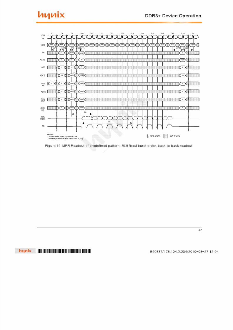
7/29/2019 DDR3 Device Operation Timing Diagram
http://slidepdf.com/reader/full/ddr3-device-operation-timing-diagram 42/154
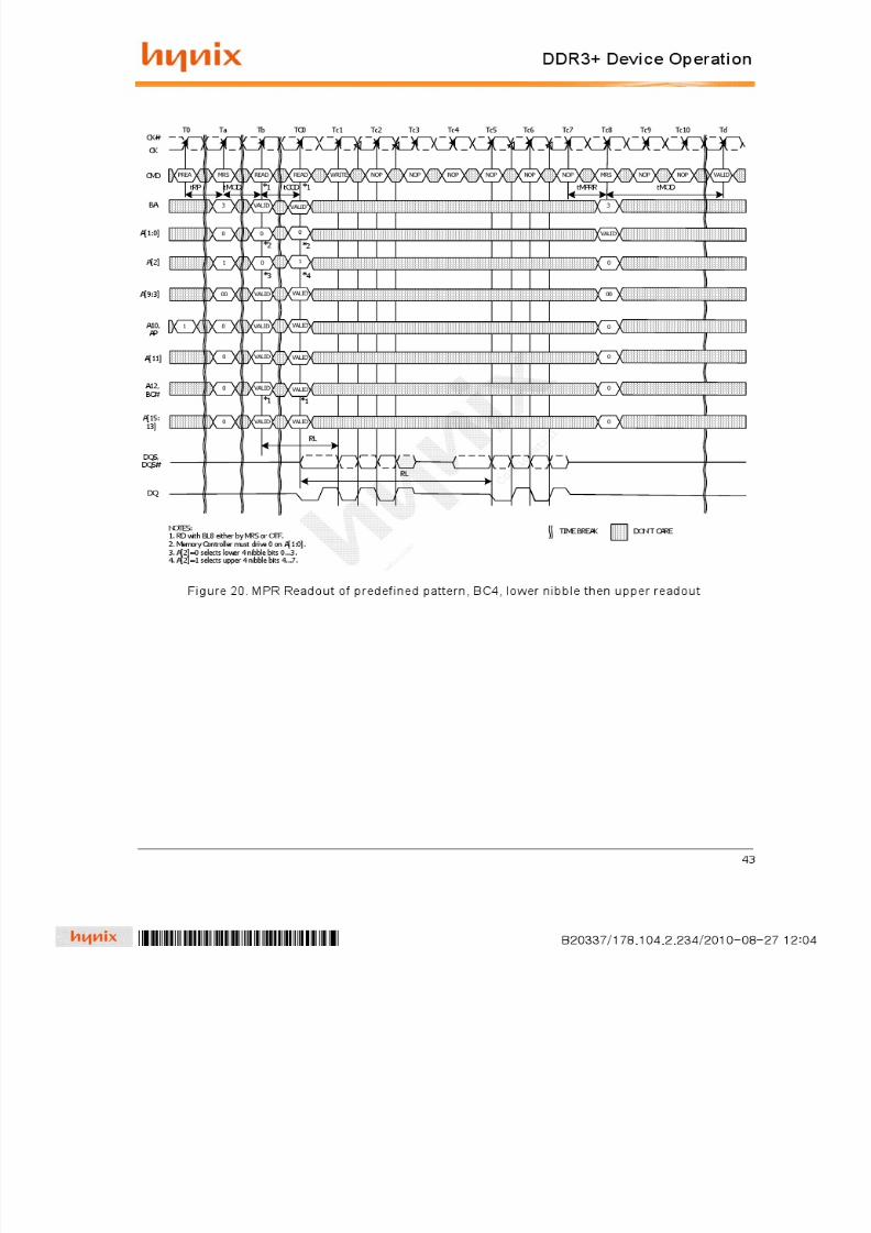
7/29/2019 DDR3 Device Operation Timing Diagram
http://slidepdf.com/reader/full/ddr3-device-operation-timing-diagram 43/154

7/29/2019 DDR3 Device Operation Timing Diagram
http://slidepdf.com/reader/full/ddr3-device-operation-timing-diagram 44/154
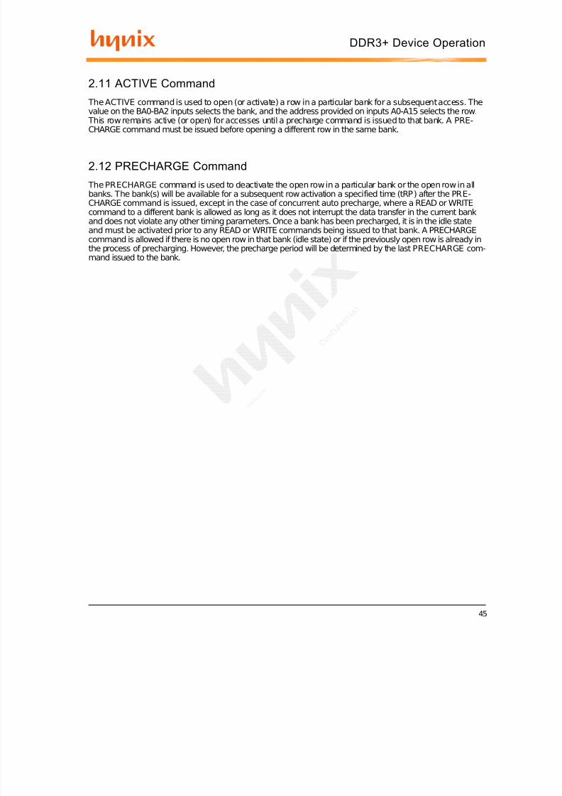
7/29/2019 DDR3 Device Operation Timing Diagram
http://slidepdf.com/reader/full/ddr3-device-operation-timing-diagram 45/154
45
DDR3+ Device Operation
2.11 ACTIVE Command
The ACTIVE command is used to open (or activate) a row in a particular bank for a subsequent access. Thevalue on the BA0-BA2 inputs selects the bank, and the address provided on inputs A0-A15 selects the row.
This row remains active (or open) for accesses until a precharge command is issued to that bank. A PRE-CHARGE command must be issued before opening a different row in the same bank.
2.12 PRECHARGE Command
The PRECHARGE command is used to deactivate the open row in a particular bank or the open row in allbanks. The bank(s) will be available for a subsequent row activation a specified time (tRP) after the PRE-CHARGE command is issued, except in the case of concurrent auto precharge, where a READ or WRITEcommand to a different bank is allowed as long as it does not interrupt the data transfer in the current bankand does not violate any other timing parameters. Once a bank has been precharged, it is in the idle stateand must be activated prior to any READ or WRITE commands being issued to that bank. A PRECHARGEcommand is allowed if there is no open row in that bank (idle state) or if the previously open row is already inthe process of precharging. However, the precharge period will be determined by the last PRECHARGE com-mand issued to the bank.

7/29/2019 DDR3 Device Operation Timing Diagram
http://slidepdf.com/reader/full/ddr3-device-operation-timing-diagram 46/154
46
DDR3+ Device Operation
2.13 READ Operation
2.13.1 READ Burst Operation
During a READ or WRITE command, DDR3 will support BC4 and BL8 on the fly using address A12 duringthe READ or WRITE(AUTO PRECHARGE can be enabled or disabled).
A12=0, BC4(BC4=burst chop, tCCD=4)
A12=1, BL8
A12 is used only for burst length control, not as a column address.
Figur e 22. READ Burst Operati on RL=5 (AL=0,CL=5,BL8)
Figur e 23. READ Burst Operati on RL=9 (AL=4,CL=5,BL8)
READ
Bank,Col n
T0CK#
CK
COMMAND3
ADDRESS4
DQS, DQS#
T1 T2 T3 T4 T5 T6 T7 T8 T9 T10
NOPNOP NOP NOP NOP MRSNOPNOP NOP NOP
tRPRE tRPST
DQ2
CL=5
Doutn
Doutn+1
Doutn+2
Doutn+3
Doutn+4
Doutn+5
Doutn+6
Doutn+7
NOTE: 1. BL8, RL=5, AL=0, CL=5.2. Dout n = data-out from column n.
3. NOP commands are shown for ease of illustration: other commands may be valid at these times.4. BL8 setting activated by either MR0[A1:0=00] or MR0[A1:0=01] and A12=1 during READ command at T0.
TRANSITIONING DATA DON’T CARE
RL=AL+CL
READ
Bank Col n
T0CK#
CK
COMMAND3
ADDRESS4
DQS, DQS#
T1 T2 T3 T4 T5 T6 T7 T8 T9 T10
NOPNOP NOP NOP NOP NOPNOPNOP NOP NOP
tRPRE
DQ2 AL=4
Doutn
Doutn+1
Doutn+2
NOTE: 1. BL8, RL=9, AL=(CL-1), CL=5.2. Dout n = data-out from column n.3. NOP commands are shown for ease of illustration; other commands may be valid at these times.4. BL8 setting activated by either MR0[A1:0=00] or MR0[A1:0=01] and A12=1 during READ command at T0.
TRANSITIONING DATA DON’T CARE
CL=5
RL=AL+CL

7/29/2019 DDR3 Device Operation Timing Diagram
http://slidepdf.com/reader/full/ddr3-device-operation-timing-diagram 47/154
47
DDR3+ Device Operation
2.13.2 READ Timing Definitions
Read timing is shown in Figure 24 and is applied when the DLL is enabled and locked.
Rising data strobe edge parameters:
• tDQSCK min/max describes the allowed range for a rising data strobe edge relative aCK,CK#.
• tDQSCK is the actual position or a rising strobe edge relative to CK,CK#.• tQSH describes the DQS,DQS#differential output high time.• tDQSQ describes the latest valid transition of the associated DQ pins.• tQH describes the earliest invalid transition of the associated DQ pins.
Falling data strobe edge parameters:
• tQSL describes the DQS,DQS#differential output low time.• tDQSQ describes the latest valid transition of the associated DQ pins.• tQH describes the earliest invalid transition of the associated DQ pins.
tDQS; both rising/falling edges of DQS, no tAC defined.
Figure 24. READ Timing Definitio n
CK#
CK
tDQSCK, MIN
tDQSCK
DQS
DQStQH
tDQSQ
CK#
tDQSQ
tQH
tQSH tQSL
CK#
tDQSCK, MAX
tDQSCK, MIN
tDQSCK, MAX
Rising StrobeRegion
Rising StrobeRegion

7/29/2019 DDR3 Device Operation Timing Diagram
http://slidepdf.com/reader/full/ddr3-device-operation-timing-diagram 48/154
48
DDR3+ Device Operation
2.13.2.1 READ Timing; Clock to Data Strobe relationship
Clock to Data Strobe relationship is shown in Figure 25 and is applied when the DLL is enabled and locked.
Rising data strobe edge parameters:
• tDQSCK min/max describes the allowed range for a rising data strobe edge relative toCK,CK#.
• tDQSCK is the actual position of a rising strobe edge relative to CK,CK#.• tQSH describes the data strobe high pulse width.
Falling data strobe edge parameters:
• tQSL describes the data strobe low pulse width.
tLZ (DQS), tHZ (DQS) for preamble/postamble (see 2.13.2.3 and Figure 27)
Figure 25. Clock to Data Strobe Relationshi p
RL Measuredto this point
CLK/CLK#
tDQSCK(min)
tLZ(DQS)min tQSH tQSL
tDQSCK(min)
tQSH tQSL
tDQSCK(min)
tQSH tQSL
tDQSCK(min)tHZ(DQS)min
tRPRE
DQS,DQS#Early Strobe
tRPST
tLZ(DQS)max
Bit0 Bit1 Bit2 Bit3 Bit4 Bit5 Bit6 Bit7
tDQSCK(max ) t DQSCK (max ) tDQSCK(max ) tDQSCK(max)tRPST
tHZ(DQS)max
Bit0 Bit1 Bit2 Bit3 Bit4 Bit5 Bit6 Bit7
DQS,DQS#Late Strobe
tQSH tQSL tQSH tQSLtRPRE
NOTE: 1. Within a burst, rising strobe edge is not necessarily fixed to be always at tDQSCK(min) or tDQSCK(max). Inst ead, rising edge can vary between tDQSCK(min) and tDQSCK(max).2. Notwithstanding note 1, a rising strobe edge with tDQSCK(max) at T(n) can not be immediately followed by a rising strobe edge with tDQSCK(min) at T(n+1). This is because other
timing relactionship (tQSH, tQSL) exist:if tDQSCK(n+1) < 0:tDQSCK(n) < 1.0 tCH ? (tQSHmin + tQSLmin) - | tDQSCK(n+1) |
2. The DQS,DQS# differential output high t ime is defined by tQSH and the DQS,DQS# differential output low time is defined by tQSL .3. Likewise, tLZ(DQS)min and tHZ(DQS)min are not tied to tDQSCKmin(early strobe case) and tLZ(DQS)max and t HZ(DQS)max are not tied to tDQSCKmax(late strobe case).4. The minimum pulse width of read preamble is defined tRPRE(min).5. The maximum read postamble is bound by tDQSCK(min( plus tQSH(min) on t he left side and tHZDSQ(max) on the right side.6. The minimum pulse width read postamble is defined by tRPST(min).7. The maximum read preamble is bound by tLZDQS(min) on the left side and tDQSCK(max) on the right side.
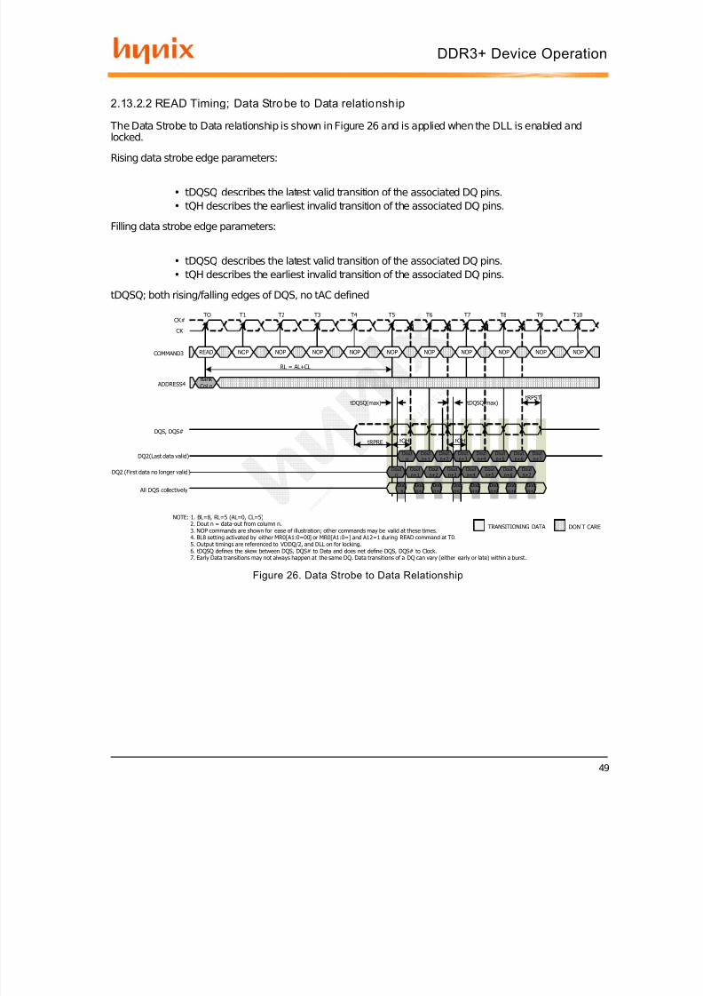
7/29/2019 DDR3 Device Operation Timing Diagram
http://slidepdf.com/reader/full/ddr3-device-operation-timing-diagram 49/154
49
DDR3+ Device Operation
2.13.2.2 READ Timing; Data Strobe to Data relationship
The Data Strobe to Data relationship is shown in Figure 26 and is applied when the DLL is enabled andlocked.
Rising data strobe edge parameters:
• tDQSQ describes the latest valid transition of the associated DQ pins.• tQH describes the earliest invalid transition of the associated DQ pins.
Filling data strobe edge parameters:
• tDQSQ describes the latest valid transition of the associated DQ pins.• tQH describes the earliest invalid transition of the associated DQ pins.
tDQSQ; both rising/falling edges of DQS, no tAC defined
Figure 26. Data Strobe to Data Relationship
READ
Bank Col n
TOCK#
CK
COMMAND3
ADDRESS4
DQS, DQS#
T1 T2 T3 T4 T5 T6 T7 T8 T9 T10
NOPNOP NOP NOP NOP NOPNOPNOP NOP NOP
tDQSQ(max)tRPST
DQ2(Last data valid)
RL = AL+CL
Dout
n
Dout
n+1
Dout
n+2
Dout
n+3
Dout
n+4
Dout
n+5
Dout
n+6
Dout
n+7Dout
nDoutn+1
Doutn+2
Doutn+4
Doutn+5
Doutn+6
Doutn+7
tRPRE tOH tOH
Doutn+3
Doutn
Doutn+1
Doutn+2
Doutn+3
Doutn+4
Doutn+6
Doutn+7
Doutn+5
NOTE: 1. BL=8, RL=5 (AL=0, CL=5)2. Dout n = data-out from column n.3. NOP commands are shown for ease of illustration; other commands may be valid at these times.4. BL8 setting activated by either MR0[A1:0=00] or MR0[A1:0=] and A12=1 during READ command at T0.5. Output timings are referenced to VDDQ/2, and DLL on for locking.6. tDQSQ defines the skew between DQS, DQS# to Data and does net define DQS, DQS# to Clock.7. Early Data transitions may not always happen at the same DQ. Data transitions of a DQ can vary (either early or late) within a burst.
TRANSITIONING DATA DON’T CARE
All DQS collectively
DQ2 (First data no longer valid )
tDQSQ(max)
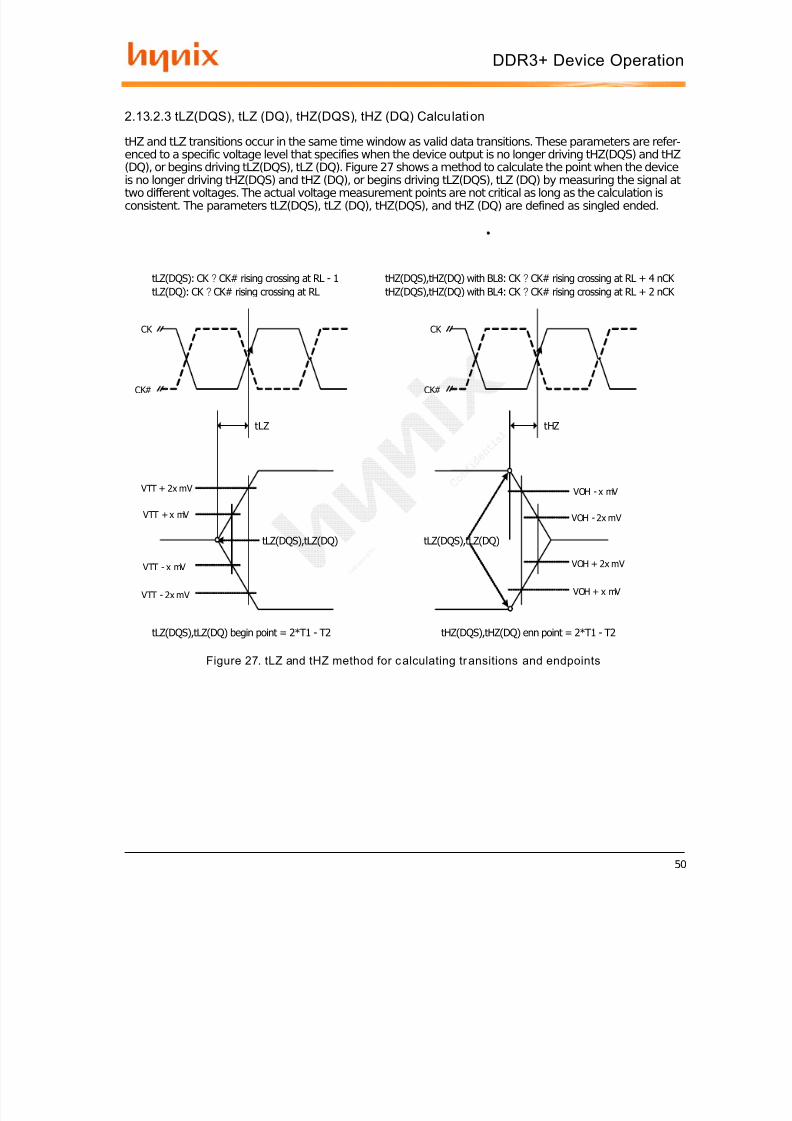
7/29/2019 DDR3 Device Operation Timing Diagram
http://slidepdf.com/reader/full/ddr3-device-operation-timing-diagram 50/154
50
DDR3+ Device Operation
2.13.2.3 tLZ(DQS), tLZ (DQ), tHZ(DQS), tHZ (DQ) Calculation
tHZ and tLZ transitions occur in the same time window as valid data transitions. These parameters are refer-enced to a specific voltage level that specifies when the device output is no longer driving tHZ(DQS) and tHZ
(DQ), or begins driving tLZ(DQS), tLZ (DQ). Figure 27 shows a method to calculate the point when the deviceis no longer driving tHZ(DQS) and tHZ (DQ), or begins driving tLZ(DQS), tLZ (DQ) by measuring the signal attwo different voltages. The actual voltage measurement points are not critical as long as the calculation isconsistent. The parameters tLZ(DQS), tLZ (DQ), tHZ(DQS), and tHZ (DQ) are defined as singled ended.
Figure 27. tLZ and tHZ method for c alculating tr ansitions and endpoints
CK#
CK
VTT + 2x mV
VTT + x mV
VTT - 2x mV
VTT - x mV
tLZ(DQS): CK ? CK# rising crossing at RL - 1tLZ(DQ): CK ? CK# rising crossing at RL
tLZ(DQS),tLZ(DQ)
tLZ(DQS),tLZ(DQ) begin point = 2*T1 - T2
tLZ
CK#
CK
tHZ(DQS),tHZ(DQ) with BL8: CK ? CK# rising crossing at RL + 4 nCK tHZ(DQS),tHZ(DQ) with BL4: CK ? CK# rising crossing at RL + 2 nCK
tHZ(DQS),tHZ(DQ) enn point = 2*T1 - T2
tHZ
VOH - x mV
VOH - 2x mV
VOH + x mV
VOH + 2x mV
tLZ(DQS),tLZ(DQ)

7/29/2019 DDR3 Device Operation Timing Diagram
http://slidepdf.com/reader/full/ddr3-device-operation-timing-diagram 51/154
51
DDR3+ Device Operation
2.13.2.4 tRPRE Calculation
Method for calculating differential pulse widths for tRPRE is shown in Figure 28.
Figure 28. Method for c alculating tRPRE transiti ons and endpo ints
2.13.2.5 tRPST Calculation
Method for calculating differential pulse widths for tRPST is shown in Figure 29.
Figure 28. Method for c alculating tRPRE transiti ons and endpo ints
CK
CK
VTT
DQS
Sibgke ebded signal, provided asbackground information
VTT
DQSSingle ebded signal, provided as
background information
VTT
tC tD
tB
DQS - DQS
Resulting Differential signal,Relevant for tRPRE specification
t1tRPRE_begin
t2
tRPRE_end
0
tA
tRPRE
CK
CK
VTT
DQS
Sibgke ebded signal, provided asbackground information
VTT
DQSSingle ebded signal, provided as
background information
VTT
tCtD
tB
DQS - DQS
Resulting Differential signal,Relevant for tRPST specification
t1tRPST_begin t2
tRPST_end
0
tA
tRPST
TD_TRPST_DEF
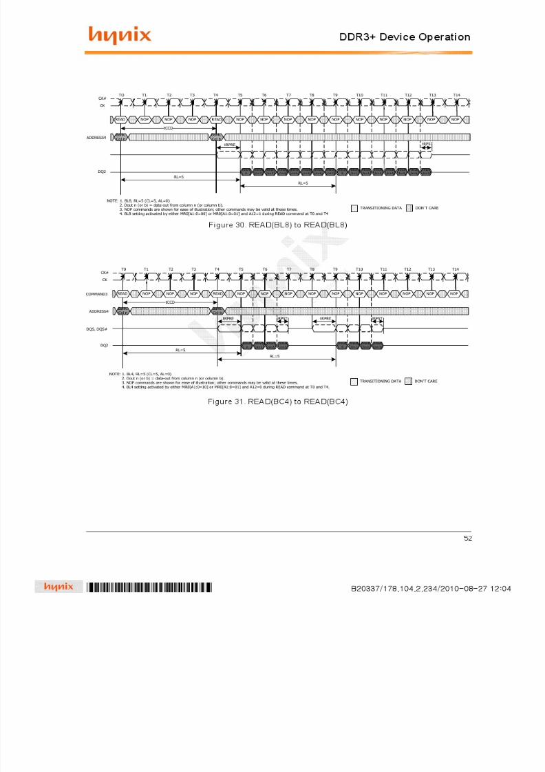
7/29/2019 DDR3 Device Operation Timing Diagram
http://slidepdf.com/reader/full/ddr3-device-operation-timing-diagram 52/154
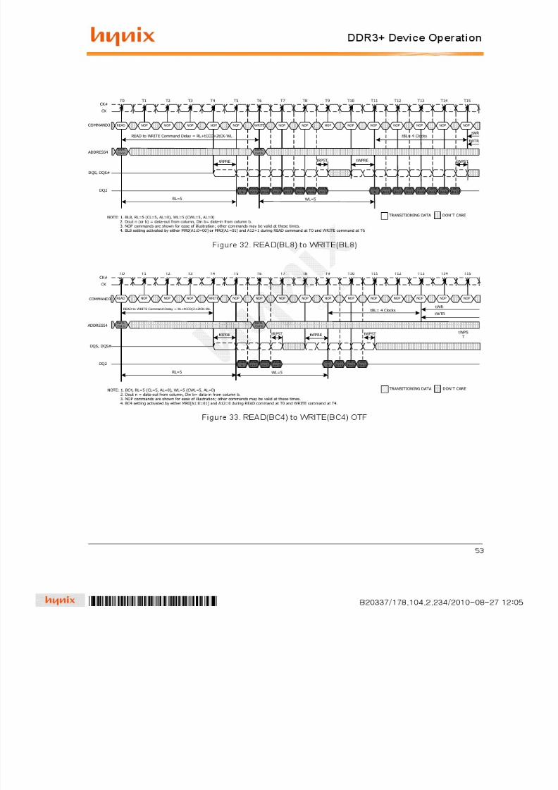
7/29/2019 DDR3 Device Operation Timing Diagram
http://slidepdf.com/reader/full/ddr3-device-operation-timing-diagram 53/154

7/29/2019 DDR3 Device Operation Timing Diagram
http://slidepdf.com/reader/full/ddr3-device-operation-timing-diagram 54/154
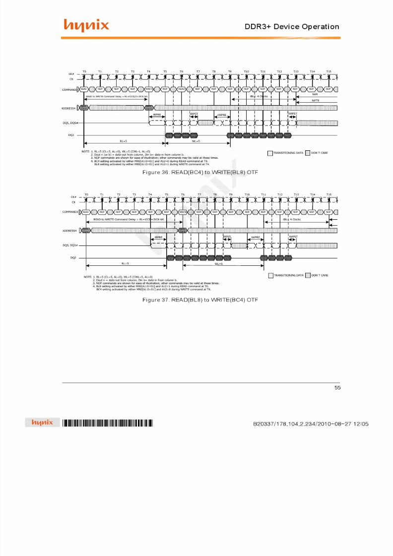
7/29/2019 DDR3 Device Operation Timing Diagram
http://slidepdf.com/reader/full/ddr3-device-operation-timing-diagram 55/154

7/29/2019 DDR3 Device Operation Timing Diagram
http://slidepdf.com/reader/full/ddr3-device-operation-timing-diagram 56/154
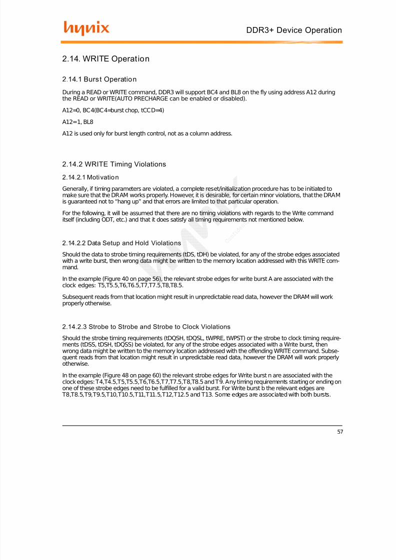
7/29/2019 DDR3 Device Operation Timing Diagram
http://slidepdf.com/reader/full/ddr3-device-operation-timing-diagram 57/154
57
DDR3+ Device Operation
2.14. WRITE Operation
2.14.1 Burs t Operation
During a READ or WRITE command, DDR3 will support BC4 and BL8 on the fly using address A12 duringthe READ or WRITE(AUTO PRECHARGE can be enabled or disabled).
A12=0, BC4(BC4=burst chop, tCCD=4)
A12=1, BL8
A12 is used only for burst length control, not as a column address.
2.14.2 WRITE Timing Violations
2.14.2.1 Motivation
Generally, if timing parameters are violated, a complete reset/initialization procedure has to be initiated tomake sure that the DRAM works properly. However, it is desirable, for certain minor violations, that the DRAMis guaranteed not to “hang up” and that errors are limited to that particular operation.
For the following, it will be assumed that there are no timing violations with regards to the Write commanditself (including ODT, etc.) and that it does satisfy all timing requirements not mentioned below.
2.14.2.2 Data Setup and Hold Violations
Should the data to strobe timing requirements (tDS, tDH) be violated, for any of the strobe edges associatedwith a write burst, then wrong data might be written to the memory location addressed with this WRITE com-mand.
In the example (Figure 40 on page 56), the relevant strobe edges for write burst A are associated with theclock edges: T5,T5.5,T6,T6.5,T7,T7.5,T8,T8.5.
Subsequent reads from that location might result in unpredictable read data, however the DRAM will workproperly otherwise.
2.14.2.3 Strobe to Strobe and Strobe to Clock Violations
Should the strobe timing requirements (tDQSH, tDQSL, tWPRE, tWPST) or the strobe to clock timing require-
ments (tDSS, tDSH, tDQSS) be violated, for any of the strobe edges associated with a Write burst, thenwrong data might be written to the memory location addressed with the offending WRITE command. Subse-quent reads from that location might result in unpredictable read data, however the DRAM will work properlyotherwise.
In the example (Figure 48 on page 60) the relevant strobe edges for Write burst n are associated with theclock edges: T4,T4.5,T5,T5.5,T6,T6.5,T7,T7.5,T8,T8.5 and T9. Any timing requirements starting or ending onone of these strobe edges need to be fulfilled for a valid burst. For Write burst b the relevant edges are
T8,T8.5,T9,T9.5,T10,T10.5,T11,T11.5,T12,T12.5 and T13. Some edges are associated with both bursts.
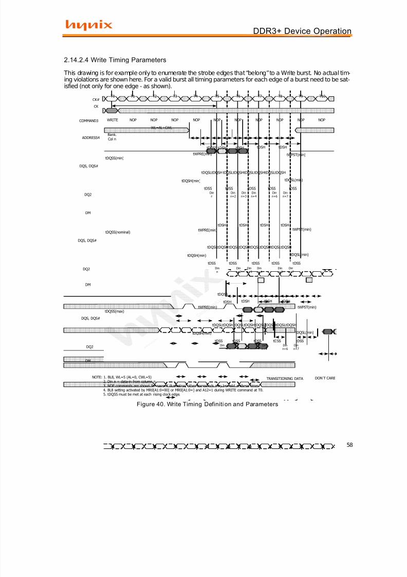
7/29/2019 DDR3 Device Operation Timing Diagram
http://slidepdf.com/reader/full/ddr3-device-operation-timing-diagram 58/154
58
DDR3+ Device Operation
2.14.2.4 Write Timing Parameters
This drawing is for example only to enumerate the strobe edges that “belong” to a Write burst. No actual tim-ing violations are shown here. For a valid burst all timing parameters for each edge of a burst need to be sat-
isfied (not only for one edge - as shown).
Figure 40. Write Timing Definiti on and Parameters
NOTE: 1. BL8, WL=5 (AL=0, CWL=5)2. Din n = data-in from column n3. NOP commands are shown for ease of illustration; other commands may be valid at these times.4. BL8 setting activated by MR0[A1:0=00] or MR0[A1:0=] and A12=1 during WRITE command at T0.5. tDQSS must be met at each rising clock edge.
T0CK#
CK
COMMAND3
ADDRESS4
DQS, DQS#
T1 T2 T3 T4 T5 T6 T7 T8 T9 T10
NOPNOP NOP NOP NOPNOPNOP NOP NOP
DQ2 Dinn
TRANSITIONING DATA DON’T CARE
WRITE NOP
Bank.Col n
Dinn+2
Dinn+3
WL=AL+CWL
tDQSS(min)
tDQSLtDQSH tDQSLtDQSHtDQSLtDQSHtDQSLtDQSH
tDQSH(min)
tDSS tDSS tDSS tDSS tDSS
tDQSL(min)
tDQSS tDSH tDSH tDSH
tWPST(min)
Dinn+4
Dinn+6
Dinn+7
Dinn
Dinn+2
Dinn+3
tWPRE(min)
tDQSLtDQSH tDQSLtDQSHtDQSLtDQSHtDQSLtDQSH
tDQSH(min)
tDSS tDSS tDSS tDSS tDSS
tDQSL(min)
tWPST(min)
Dinn+4
Dinn+6
Dinn+7
Dinn
Dinn+2
Dinn+3
tWPRE(min)
tDQSLtDQSH tDQSLtDQSHtDQSLtDQSHtDQSLtDQSH
tDQSH(min)
tDSS tDSS tDSS tDSS tDSS
tDQSL(min)
tDQSS
tDSH tDSH tDSH
tWPST(min)
Dinn+4
Dinn+6
Dinn+7
tDSH tDSH tDSH tDSH
tWPRE(min)
tDSH
DQS, DQS#
DQ2
DQS, DQS#
DQ2
tDSH
tDQSS(nominal)
tDQSS(max)
DM
DM
DM

7/29/2019 DDR3 Device Operation Timing Diagram
http://slidepdf.com/reader/full/ddr3-device-operation-timing-diagram 59/154
59
DDR3+ Device Operation
2.14.3 Write Data Mask
One write data mask (DM) pin for each 8 data bits (DQ) will be supported on DDR3 SDRAMs, consistent withthe implementation on DDR2 SDRAMs. It has identical timings on write operations as the data bits as shown
in Figure 40, and though used in a unidirectional manner, is internally loaded identically to data bits to ensurematched system timing. DM is not used during read cycles for any bit organizations including x4, x8, and x16,however, DM of x8 bit organization can be used as TDQS during write cycles if enabled by the MR1[A11] set-ting. See 1.4.3.7 “TDQS,TDQS” on page 16 for more details on TDQS vs. DM operations.
2.14.4 tWPRE Calculation
The method for calculating differential pulse widths for tWPRE is shown in Figure 41.
Figure 41. Method f or calcul ating tWPRE transition s and endpoint
2.14.5 tWPST Calculation
The method for calculating differential pulse widths for tWPST is shown in Figure 42.
Figure 42. Method for calculating t WPST transition s and endpoint
CK
CK
Resulting differential signalRelevant for t WPRE
spectification
VTT
0 VDQS - DQStWPRE
t1tWPRE_begin ’
t2tWPRE_end
CK
CK
Resulting differential signalRelevant for t WPST
spectification
VTT
0 VDQS - DQStWPST
t2tWPST_end
t1tWPST_begin
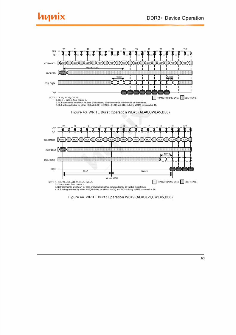
7/29/2019 DDR3 Device Operation Timing Diagram
http://slidepdf.com/reader/full/ddr3-device-operation-timing-diagram 60/154
60
DDR3+ Device Operation
Figur e 43. WRITE Burs t Operatio n WL=5 (AL=0,CWL=5,BL8)
Figur e 44. WRITE Burs t Operatio n WL=9 (AL=CL-1,CWL=5,BL8)
T0CK#CK
COMMAND3
ADDRESS4
DQS, DQS#
T1 T2 T3 T4 T5 T6 T7 T8 T9 T10
NOPNOP NOP NOP NOP NOPNOPNOP NOP NOP
tWPRE
DQ3 Doutn
WRITE
Bank.Col n
Doutn+5
Doutn+6
Doutn+7
Doutn+1
Doutn+2
Doutn+3
Doutn+4
WL=AL+CWL
tWPST
NOTE: 1. BL=8, WL=5; CWL=5.2. Din n = data-in from column n.
3. NOP commands are shown for ease of illustration; other commands may be valid at these times.4. BL8 setting activated by either MR0[A1:0=00] or MR0[A1:0=01] and A12=1 during WRITE command at T0.
TRANSITIONING DATA DON’T CARE
T0CK#
CK
COMMAND3
ADDRESS4
DQS, DQS#
T1 T2 T3 T4 T5 T6 T7 T8 T9 T10
NOPNOP NOP NOP NOP NOPNOPNOP NOP NOP
tWPRE
DQ3 Doutn
WRITE
Bank.Col n
Doutn+1
Doutn+2
Doutn+3
NOTE: 1. BL8, WL=9;AL=(CL-1), CL=5, CWL=5.2. Din n=data-in from column n.3. NOP commands are shown for ease of illustration; other commands may be valid at these t imes.4. BL8 setting activated by either MR0[A1:0=00] or MR0[A1:0=01] and A12=1 during WRITE command at T0.
TRANSITIONING DATA DON’T CARE
CWL=5 AL=4
WL=AL+CWL

7/29/2019 DDR3 Device Operation Timing Diagram
http://slidepdf.com/reader/full/ddr3-device-operation-timing-diagram 61/154
61
DDR3+ Device Operation
Figur e 45. WRITE (BC4) to READ (BC4) Operatio n
Figur e 46. WRITE (BC4) to PRECHARGE Operation
T0CK#
CK
COMMAND3
ADDRESS4
DQS, DQS#
T1 T2 T3 T4 T5 T6 T7 T8 T9 Tn
NOPNOP NOP NOP NOPNOP NOP NOP
tWPST
DQ2WL=5
Dinn
TRANSITIONING DATA DON’T CARE
WRITE NOP
Bank.Col n
Bank.Col b
Dinn+1
Dinn+2
Dinn+3
NOTE: 1. BC4, WL=5, RL=5.2. Din n = data-in from column n; Dout b= data-out form column b.3. NOP commands are shown for ease of illustration; other commands may be valid at these times.4. BC=4 setting activated by MR0[A1:0=10] during WRITE command at T0 and READ command at Tn.5. tWTR controls the write to read delay to the same device and starts with the first rising clock edge after the last write data shown at T7.
READ
tWRTS5
tWPRE
T0CK#
CK
COMMAND3
ADDRESS4
DQS, DQS#
T1 T2 T3 T4 T5 T6 T7 T8 T9 Tn
NOPNOP NOP NOP NOPNOP NOP NOP
tWPST
DQ2WL=5
Dinn
TRANSITIONING DATA DON’T CARE
WRITE NOP
Bank.Col n
Dinn+1
Dinn+2
Dinn+3
NOTE: 1. BC4, WL=5, RL=5.2. Din n = data-in from column n; Dout b= data-out form column b.3. NOP commands are shown for ease of illustration; other commands may be valid at these times.4. BC4 setting activated by MR0[A1:0=10] during WRITE command at T0.5. The write recovery time(tWR) referenced from the first rising clock edge after the last write data shown at T7.
tWR specifies the last burst write cycle until the precharge command can be issued to the same bank.
PRE
tWR5
tWPRE
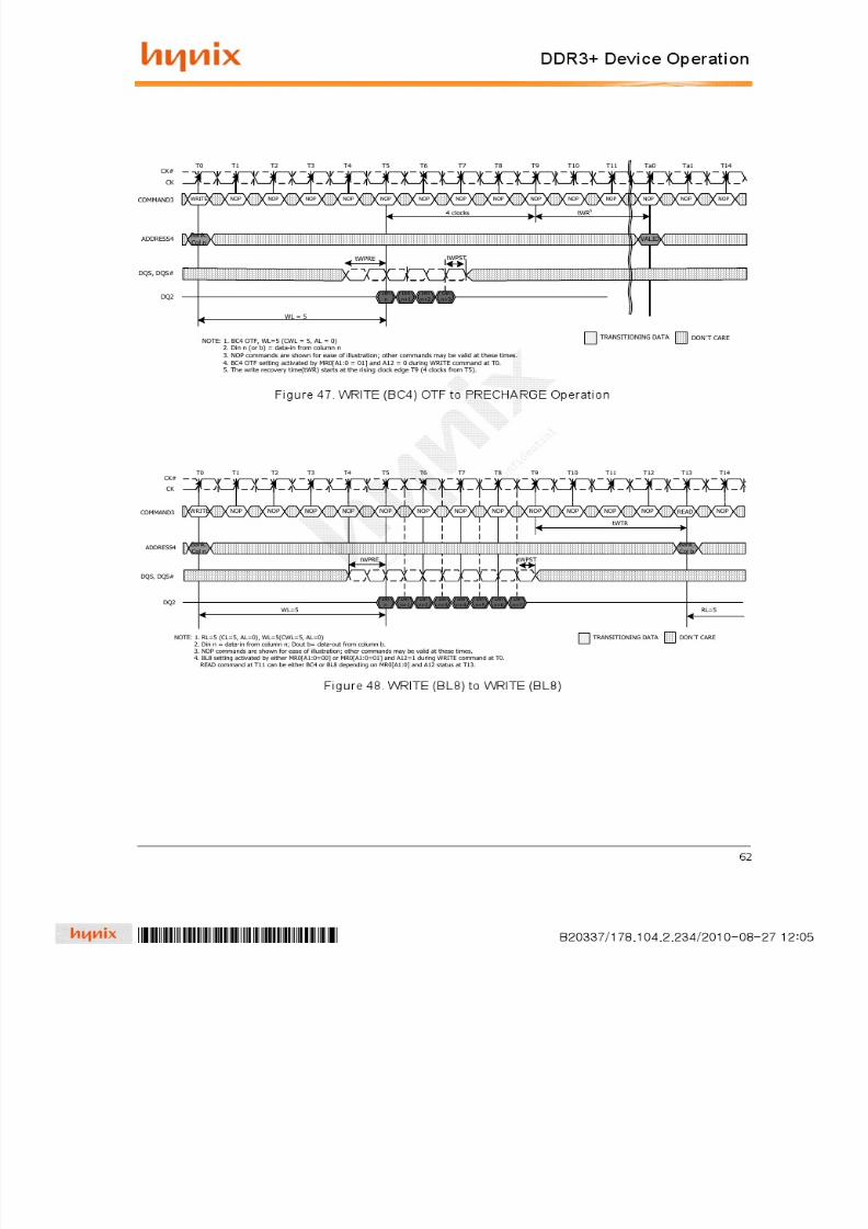
7/29/2019 DDR3 Device Operation Timing Diagram
http://slidepdf.com/reader/full/ddr3-device-operation-timing-diagram 62/154
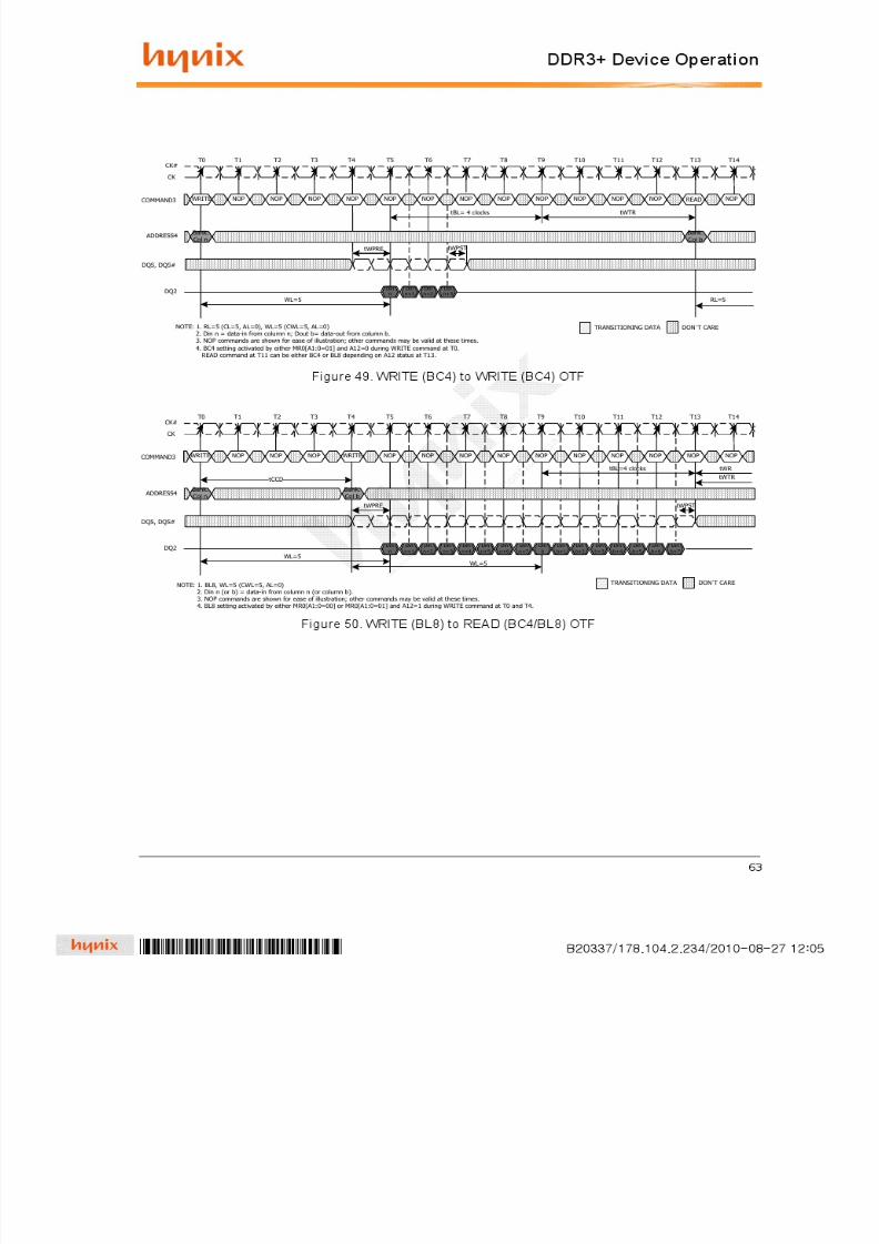
7/29/2019 DDR3 Device Operation Timing Diagram
http://slidepdf.com/reader/full/ddr3-device-operation-timing-diagram 63/154

7/29/2019 DDR3 Device Operation Timing Diagram
http://slidepdf.com/reader/full/ddr3-device-operation-timing-diagram 64/154
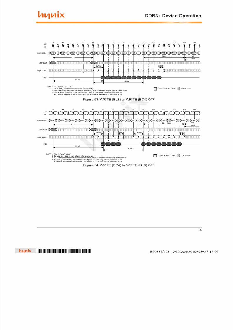
7/29/2019 DDR3 Device Operation Timing Diagram
http://slidepdf.com/reader/full/ddr3-device-operation-timing-diagram 65/154
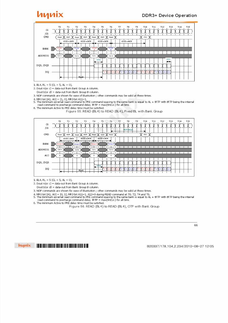
7/29/2019 DDR3 Device Operation Timing Diagram
http://slidepdf.com/reader/full/ddr3-device-operation-timing-diagram 66/154

7/29/2019 DDR3 Device Operation Timing Diagram
http://slidepdf.com/reader/full/ddr3-device-operation-timing-diagram 67/154

7/29/2019 DDR3 Device Operation Timing Diagram
http://slidepdf.com/reader/full/ddr3-device-operation-timing-diagram 68/154
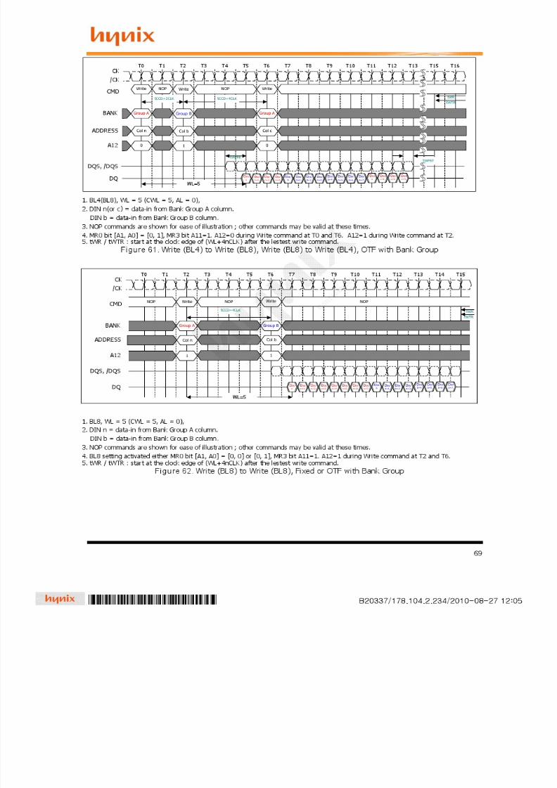
7/29/2019 DDR3 Device Operation Timing Diagram
http://slidepdf.com/reader/full/ddr3-device-operation-timing-diagram 69/154

7/29/2019 DDR3 Device Operation Timing Diagram
http://slidepdf.com/reader/full/ddr3-device-operation-timing-diagram 70/154
70
1. WL = 5 (CWL = 5, AL = 0, BL4), RL = 5 (CL=5, AL=0, BL4)
2. Din n = data-in from Bank Group A column.Dout b = data-out from Bank Group A column .
3. NOP commands are shown for ease of illustration ; other commands may be valid at these times.4. MR0 bit [A1, A0] = [1, 0], MR3 bit A11=1.5. tWR : start at the clock edge of (WL+2nCLK) after the lestest write command.
tWTR = max (4nCLK, 7.5ns)Figure 63. Write (BL4) to Read (BL4), Fixed BL with Same Bank Group
1. WL = 5 (CWL = 5, AL = 0, BL4), RL = 5 (CL=5, AL=0, BL4)2. Din n = data-in from Bank Group A column.
Dout b = data-out from Bank Group B column . 3. NOP commands are shown for ease of illustration ; other commands may be valid at these times.4. MR0 bit [A1, A0] = [1, 0], MR3 bit A11=1.5. tWR : start at the clock edge of (WL+2nCLK) after the lestest write command.
tWTR = max (2nCLK max, 3.75ns)Figure 64. Write (BL4) to Read (BL4), Fixed BL with Different Bank Group
Col n
T0 T1
Write
T2 T3 T4 T5 T6 T7 T8 T9 T10 T11 T16 T17 T18
RL=5WL=5
CK /CK
CMD
ADDRESS
DQS, /DQS
DQ
NOP NOP
DINn
DINn+1
DINn+3
DINn+2
tWPSTtWPRE
Col b
Read
tRPST
DOUT
bDOUT
b+1DOUT
b+3DOUT
b+2
T15
tRPRE
Group A BANK Group A
tWTR
Group A
T0 T1
Write
T2 T3 T4 T5 T6 T7 T8 T9 T10 T12 T14 T15 T16
RL=5WL=5
CK /CK
CMD
BANK
DQS, /DQS
DQ
NOP NOP
DINn
DINn+1
DINn+3
DINn+2
tWPSTtWPRE
Group B
Read
tRPST
DOUT
bDOUT
b+1DOUT
b+3DOUT
b+2
T13
tRPRE
tWTR
Col n ADDRESS Col b

7/29/2019 DDR3 Device Operation Timing Diagram
http://slidepdf.com/reader/full/ddr3-device-operation-timing-diagram 71/154

7/29/2019 DDR3 Device Operation Timing Diagram
http://slidepdf.com/reader/full/ddr3-device-operation-timing-diagram 72/154

7/29/2019 DDR3 Device Operation Timing Diagram
http://slidepdf.com/reader/full/ddr3-device-operation-timing-diagram 73/154
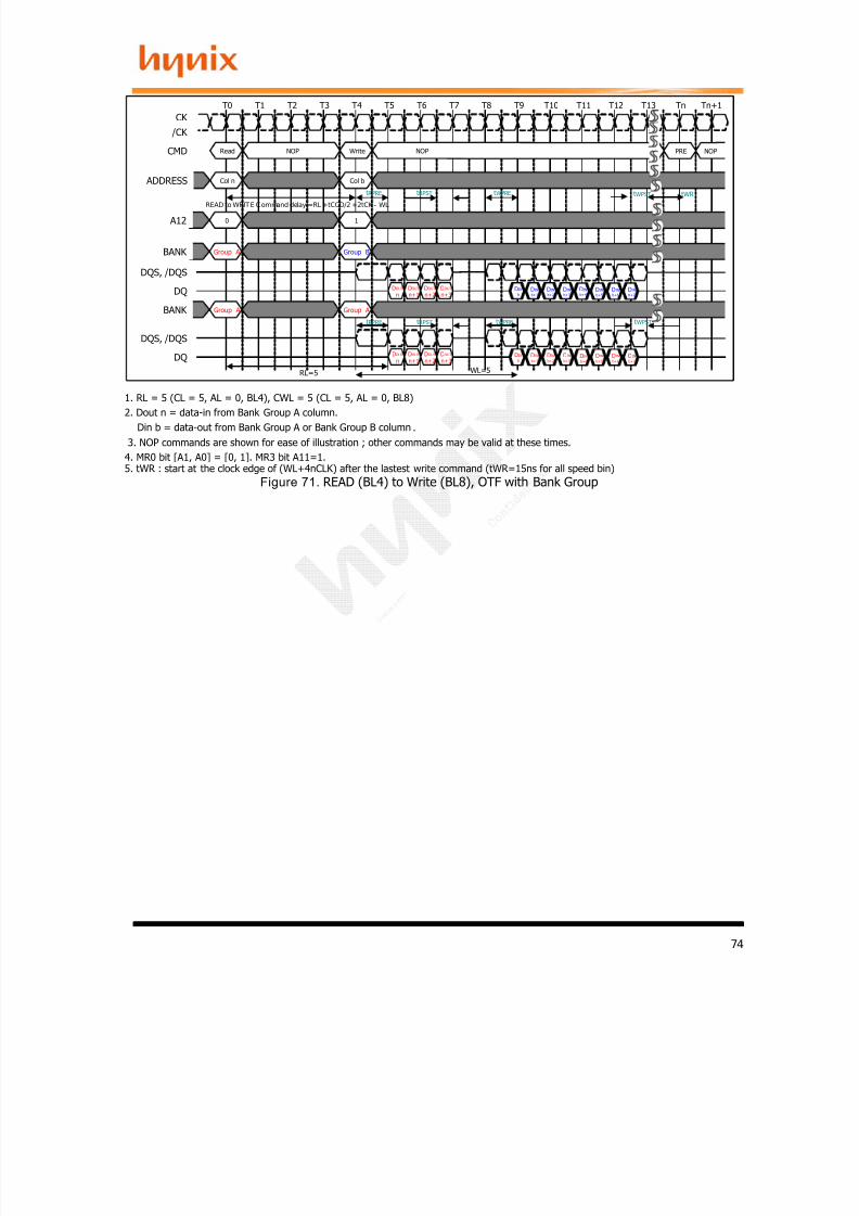
7/29/2019 DDR3 Device Operation Timing Diagram
http://slidepdf.com/reader/full/ddr3-device-operation-timing-diagram 74/154
74
1. RL = 5 (CL = 5, AL = 0, BL4), CWL = 5 (CL = 5, AL = 0, BL8)2. Dout n = data-in from Bank Group A column.
Din b = data-out from Bank Group A or Bank Group B column .3. NOP commands are shown for ease of illustration ; other commands may be valid at these times.
4. MR0 bit [A1, A0] = [0, 1]. MR3 bit A11=1.5. tWR : start at the clock edge of (WL+4nCLK) after the lastest write command (tWR=15ns for all speed bin)
Figure 71. READ (BL4) to Write (BL8), OTF with Bank Group
Col n
T0 T1
Read
T2 T3 T4 T5 T6 T7 T8 T9 T10 T11 T12 T13 Tn Tn+1
WL=5RL=5
CK /CK
CMD
ADDRESS
DQS, /DQS
DQ
Col b
DOUT
nDOUT
n+1DOUT
n+3DOUT
n+2DINb+1
DINb+3
DINb+2
DINb
WriteNOP NOP
READ to WRITE Command delay =RL +tCCD/2 +2tCK - WL
Group A BANK Group B
tRPSTtRPRE tWPRE
DQS, /DQS
DQ DOUT
nDOUT
n+1DOUT
n+3DOUT
n+2DINb+1
DINb+3
DINb+2
DINb
Group A BANK Group A
tRPSTtRPRE
PRE NOP
tWPST
tWPST
DINb+5
DINb+7
DINb+6
DINb+4
DINb+5
DINb+7
DINb+6
DINb+4
tWR
0 A12 1
tWPRE
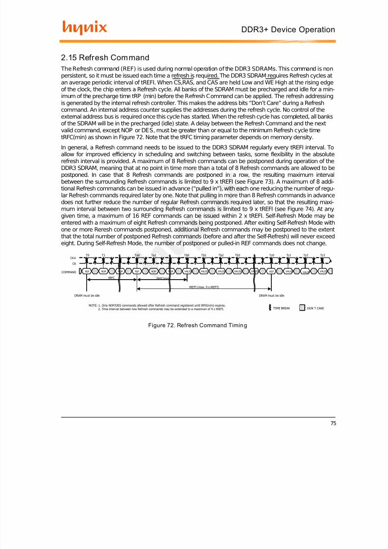
7/29/2019 DDR3 Device Operation Timing Diagram
http://slidepdf.com/reader/full/ddr3-device-operation-timing-diagram 75/154
75
DDR3+ Device Operation
2.15 Refresh Command The Refresh command (REF) is used during normal operation of the DDR3 SDRAMs. This command is nonpersistent, so it must be issued each time a refresh is required. The DDR3 SDRAM requires Refresh cycles at
an average periodic interval of tREFI. When CS,RAS, and CAS are held Low and WE High at the rising edgeof the clock, the chip enters a Refresh cycle. All banks of the SDRAM must be precharged and idle for a min-imum of the precharge time tRP (min) before the Refresh Command can be applied. The refresh addressingis generated by the internal refresh controller. This makes the address bits “Don’t Care” during a Refreshcommand. An internal address counter supplies the addresses during the refresh cycle. No control of theexternal address bus is required once this cycle has started. When the refresh cycle has completed, all banksof the SDRAM will be in the precharged (idle) state. A delay between the Refresh Command and the nextvalid command, except NOP or DES, must be greater than or equal to the minimum Refresh cycle timetRFC(min) as shown in Figure 72. Note that the tRFC timing parameter depends on memory density.
In general, a Refresh command needs to be issued to the DDR3 SDRAM regularly every tREFI interval. Toallow for improved efficiency in scheduling and switching between tasks, some flexibility in the absoluterefresh interval is provided. A maximum of 8 Refresh commands can be postponed during operation of the
DDR3 SDRAM, meaning that at no point in time more than a total of 8 Refresh commands are allowed to bepostponed. In case that 8 Refresh commands are postponed in a row, the resulting maximum intervalbetween the surrounding Refresh commands is limited to 9 x tREFI (see Figure 73). A maximum of 8 addi-tional Refresh commands can be issued in advance (“pulled in”), with each one reducing the number of regu-lar Refresh commands required later by one. Note that pulling in more than 8 Refresh commands in advancedoes not further reduce the number of regular Refresh commands required later, so that the resulting maxi-mum interval between two surrounding Refresh commands is limited to 9 x tREFI (see Figure 74). At anygiven time, a maximum of 16 REF commands can be issued within 2 x tREFI. Self-Refresh Mode may beentered with a maximum of eight Refresh commands being postponed. After exiting Self-Refresh Mode withone or more Reresh commands postponed, additional Refresh commands may be postponed to the extentthat the total number of postponed Refresh commands (before and after the Self-Refresh) will never exceedeight. During Self-Refresh Mode, the number of postponed or pulled-in REF commands does not change.
Figure 72. Refresh Command Timin g
TIME BREAK DON’T CARENOTE: 1. Only NOP/DES commands allowed after Refresh command registered until tRFE(min) expires.
2. Time interval between two Refresh commands may be extended to a maximum of 9 x tREFI.
T0CK#
CK
T1 Ta0 Ta1 Tb0 Tb1 Tb2 Tb3 Tc0 Tc1 Tc2 Tc3
COMMAND
tRFC(min)
NOPNOP NOP REF NOPREF REF VALID VALID VALID VALID VALID VALID VALID VALID
tRFC
tREFI (max. 9 x tREFI)
DRAM must be idle DRAM must be idle

7/29/2019 DDR3 Device Operation Timing Diagram
http://slidepdf.com/reader/full/ddr3-device-operation-timing-diagram 76/154
76
DDR3+ Device Operation
Figure 73. Postpo ning Refresh Commands (Example)
Figure 74. Pulling-in Refresh Commands (Example)
9 x t REFI
8 REF-Commands postponed
tREFI
tRFC
t
9 x t REFI
8 REF-Commands postponed
tREFI
tRFC
t

7/29/2019 DDR3 Device Operation Timing Diagram
http://slidepdf.com/reader/full/ddr3-device-operation-timing-diagram 77/154
77
DDR3+ Device Operation
2.16 Self-Refresh Operation The Self-Refresh command can be used to retain data in the DDR3 SDRAM, even if the rest of the system ispowered down. When in the Self-Refresh mode, the DDR3 SDRAM retains data without external clocking.
The DDR3 SDRAM device has a built-in timer to accommodate Self-Refresh operation. The Self-Refresh-Entry (SRE) Command is defined by having CS, RAS, CAS, and CKE held low with WE high at the risingedge of the clock.
Before issuing the Self-Refresh-Entry command, the DDR3 SDRAM must be idle with all bank prechargestate with tRP satisfied. Also, on-die termination must be turned off before issuing Self-Refresh-Entry com-mand, by either registering ODT pin low “ODTL +0.5tCK” prior to the Self-Refresh Entry command or usingMRS to MR1 command. Once the Self-Refresh Entry command is registered, CKE must be held low to keepthe device in Self-Refresh mode. During normal operation (DLL on), MR1(A0=0), the DLL is automatically dis-abled upon entering Self-Refresh and is automatically enabled (including a DLL-Reset) upon exiting Self-Refresh.
When the DDR3 SDRAM has entered Self-Refresh mode , all of the external control signals, except CKE andRESET, are “don’t care”. For proper Self-Refresh operation, all power supply and reference pins (VDD,VDDQ, VSS, VSSQ, VRefCA and VRefDQ) must be at valid levels. VrefDQ supply may be turned OFF andVREFDQ may take any value between VSS and VDD during self-Refresh operation, provided that VrefDQ isvalid and stable prior to CKE going back High and that first Write operation or first Write Leveling Activity maynot occur earlier than 512 nCK after exit from Self-Refresh. The DRAM initiates a minimum of one Refreshcommand internally within tCKE period once it enters Sell-Refresh mode.
The clock is internally disabled during Self-Refresh Operation to save power. The minimum time that theDDR3 SDRAM must remain in Self-Refresh mode is tCKESR. The user may change the external clock fre-quency or halt the external clock tCKSRE after Self-Refresh entry is registered, however, the clock must berestarted and stable tCKSRX before the device can exit Self-Refresh operation.
The procedure for exiting Self-Refresh requires a sequence of events. First, the clock must be stable prior toCKE going back HIGH. Once a Self-Refresh Exit command (SRX, combination of CKE going high and eitherNOP or Deselect on command bus) is registered, a delay of at least tXS must be satisfied before a valid com-mand not requiring a locked DLL can be issued to the device to allow for any internal refresh in progress.Before a command which requires a locked DLL can be applied, a delay of at least tXSDLL and applicableZQCAL function requirements (TBD) must be satisfied.
Before a command that requires a locked DLL can be applied, a delay of at least tXSDLL must be satisfied.Depending on the system environment and the amount of time spent in Self-Refresh, ZQ calibration com-mands may be required to compensate for the voltage and temperature drift as described in “ZQ CalibrationCommands” on page 76. To issue ZQ calibration commands, applicable timing requirements must be satis-fied (See Figure 72 - “ZQ Calibration Timing” on page 77).
CKE must remain HIGH for the entire Self-Refresh exit period tXSDLL for proper operation except for Self-Refresh re-entry. Upon exit from Self-Refresh, the DDR3 SDRAM can be put back into Self-Refresh mode
after waiting at least tXS period and issuing one refresh command (refresh period of tRFC). NOP or deselectcommands must be registered on each positive clock edge during the Self-Refresh exit interval tXS. ODTmust be turned off during tXSDLL.

7/29/2019 DDR3 Device Operation Timing Diagram
http://slidepdf.com/reader/full/ddr3-device-operation-timing-diagram 78/154
78
DDR3+ Device Operation
Figure 75. Self-Refresh Entr y/Exit Timing
T0 T1
CK CK#
CKE
ODT
ADDR
T2 Ta0 Tb0 Tc0 Tc1
tCKSRE
Td0 Te0 Tf0
VALID VALID
VALID
NOP SRE NOP NOP(1) VALID(2) VALID(3)SRXCOMMAND
VALID VALID
tCPDEDtIS tCKSRX
tCKESR tIS
ODTL
tRP tXS
tXSDLL
Enter Self Refresh Exit Self RefreshDON’T CARE TIME BREAK
NOTES: 1. Only NOP or DES command.2. Valid commands not requiring a locked DLL.3. Valid commands requiring a locked DLL.

7/29/2019 DDR3 Device Operation Timing Diagram
http://slidepdf.com/reader/full/ddr3-device-operation-timing-diagram 79/154
79
DDR3+ Device Operation
2.17 Power-Down Modes
2.17.1 Power-Down Entry and Exit
Power-down is synchronously entered when CKE is registered low (along with NOP or Deselect command).CKE is not allowed to go low while mode register set command, MPR operations, ZQCAL operations, DLLlocking or read / write operation are in progress. CKE is allowed to go low while any of other operations suchas row activation, precharge or auto-precharge and refresh are in progress, but power-down IDD spec will notbe applied until finishing those operations. Timing diagrams are shown in Figures 59 through Figures 71 withdetails for entry and exit of Power-Down.
The DLL should be in a locked state when power-down is entered for fastest power-down exit timing. If theDLL is not locked during power-down entry, the DLL must be reset after exiting power-down mode for properread operation and synchronous ODT operation. DRAM design provides all AC and DC timing and voltagespecification as well as proper DLL operation with any CKE intensive operations as long as DRAM controllercomplies with DRAM specifications.
During Power-Down, if all banks are closed after any in-progress commands are completed, the device willbe in precharge Power-Down mode; if any bank is open after in-progress commands are completed, thedevice will be in active Power-Down mode.
Entering power-down deactivates the input and output buffers, excluding CK, CK, ODT, CKE and RESET. Toprotect DRAM internal delay on CKE line to block the input signals, multiple NOP or Deselect commands areneeded during the CKE switch off and cycle(s) after, this timing period are defined as tCPDED. CKE_low willresult in deactivation of command and address receivers after tCPDED has expired.
Also , the DLL is disabled upon entering precharge power-down (Slow Exit Mode) , but the DLL is kept enabledduring precharge power-down (Fast Exit Mode) or active power-down. In power-down mode, CKE low,RESET high and a stable clock signal must be maintained at the inputs of the DDR3 SDRAM, and ODT
should be in a valid state, but all other input signals are “Don’t Care” (If RESET goes low during Power-Down,the DRAM will be out of PD mode and into reset state .) CKE low must be maintained until tCKE has been sat-isfied. P ower-down duration is limited by 9 times tREFI of the device.
The power-down state is synchronously exited when CKE is registered high (along with a NOP or Deselectcommand). CKE high must be maintained until tCKE has been satisfied. A valid, executable command can beapplied with power-down exit latency, tXP and/or tXPDLL after CKE goes high. Power-down exit latency isdefined in the AC specifications table of this data sheet.
Active Power Down Entry and Exit timing diagram example is shown in Figure 76. Timing Diagrams for CKEwith PD Entry, PD Exit with Read and Read with Auto Precharge, Write, Write with Auto Precharge, Activate,Precharge, Refresh, and MRS are shown in Figure 77 through Figure 85. Additional clarifications are shownin Figure 86 through Figure 88.
Table 13. Power-Down Entry Definit ions
Status of DRAMMRSbit A12 DLL PD Exit Relevant Parameters
Active
(A bank or more Open)
Don’t
CareOn Fast tXP to any valid command
Precharged(All banks Precharged) 0 Off Slow
tXP to any valid command. Since it is in prechargestate, commands here will be ACT,REF,MRS,PRE orPREA. tXPDLL to commands that need the DLL to operate,such as RD,RDA or ODT control line.
Precharged(All banks Precharged) 1 On Fast tXP to any valid command.
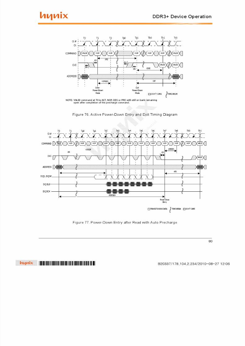
7/29/2019 DDR3 Device Operation Timing Diagram
http://slidepdf.com/reader/full/ddr3-device-operation-timing-diagram 80/154

7/29/2019 DDR3 Device Operation Timing Diagram
http://slidepdf.com/reader/full/ddr3-device-operation-timing-diagram 81/154

7/29/2019 DDR3 Device Operation Timing Diagram
http://slidepdf.com/reader/full/ddr3-device-operation-timing-diagram 82/154
82
DDR3+ Device Operation
Figure 80. Precharge Power-Down (Fast Exit Mode) Entry and Exit
Figure 81. Precharge Power-Down (Slow Exit Mode) Entry and Exit
T0 T1
CK CK#
CKE
T2 Ta0 Ta1 Tb0 Tb1 Tc0
VALID VALID
tCPDEDtIS
tPD
Enter Exit
DON’T CARE TIME BREAK
NOP NOP VALIDCOMMAND NOPNOP NOP
tIS
tIH
tXP
Power-DownMode
Power-DownMode
T0 T1
CK CK#
CKE
T2 Ta0 Ta1 Tb0 Tb1 Tc0
VALID
tCPDEDtIS
tPD
Enter Exit
DON’T CARE TIME BREAK
NOP NOPCOMMAND NOPNOP NOP
tIS
tIH
tXP
Power-DownMode
Power-DownMode
Td0
VALID VALID
VALID VALID
tXPDLL
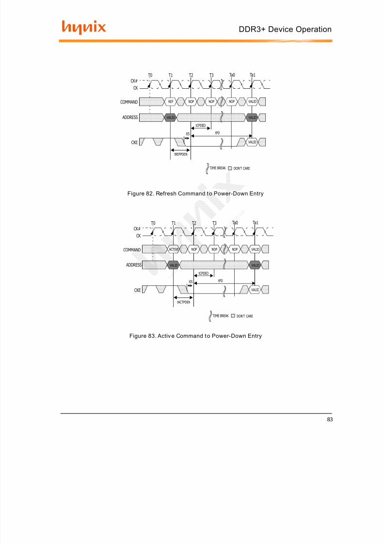
7/29/2019 DDR3 Device Operation Timing Diagram
http://slidepdf.com/reader/full/ddr3-device-operation-timing-diagram 83/154
83
DDR3+ Device Operation
Figure 82. Refresh Command t o Power-Down Entry
Figure 83. Activ e Command t o Power-Down Entry
T0 T1
CK CK#
CKE
T2 T3 Ta0 Ta1
VALID
tIS
tREFPDEN
DON’T CARETIME BREAK
REF NOPCOMMAND NOPNOP VALID
VALID VALID
tCPDED
tPD
ADDRESS
T0 T1
CK CK#
CKE
T2 T3 Ta0 Ta1
VALID
tIS
tACTPDEN
DON’T CARETIME BREAK
ACTIVE NOPCOMMAND
NOPNOP VALID
VALID VALID
tCPDED
tPD
ADDRESS
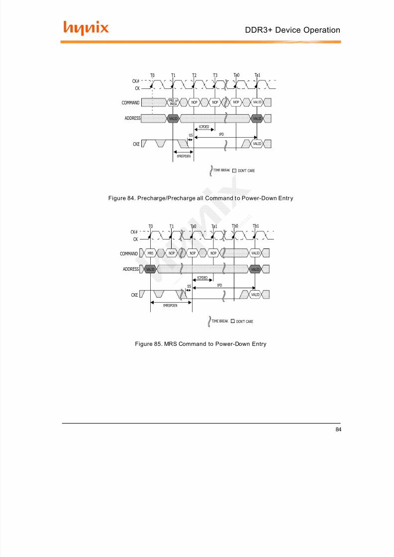
7/29/2019 DDR3 Device Operation Timing Diagram
http://slidepdf.com/reader/full/ddr3-device-operation-timing-diagram 84/154
84
DDR3+ Device Operation
Figure 84. Precharge/Precharge all Command t o Power-Down Entr y
Figure 85. MRS Command to Power-Down Entry
T0 T1
CK CK#
CKE
T2 T3 Ta0 Ta1
VALID
tIS
tPREPDEN
DON’T CARETIME BREAK
PRE or NOPCOMMAND NOPNOP VALID
VALID VALID
tCPDED
tPD
ADDRESS
PREA
T0 T1
CK CK#
CKE
Ta0 Ta1 Tb0 Tb1
VALID
tIS
tMRSPDEN
DON’T CARETIME BREAK
NOPCOMMAND NOP VALID
VALID VALID
tCPDED
tPD
ADDRESS
NOPMRS
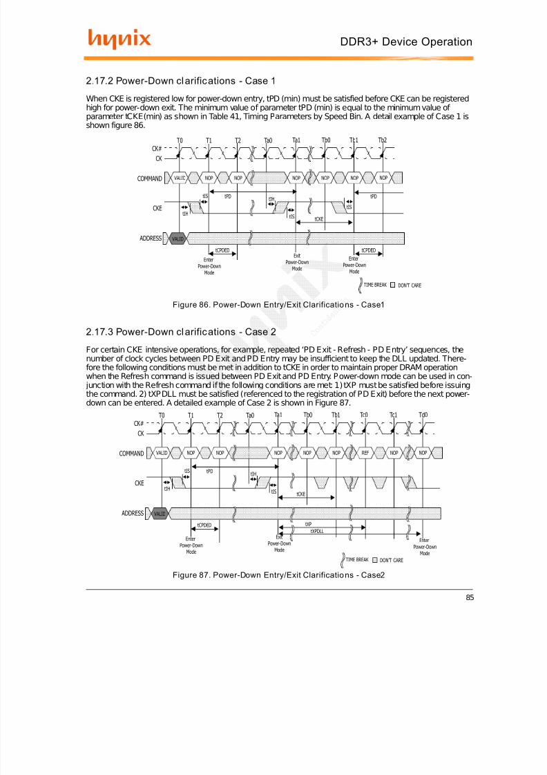
7/29/2019 DDR3 Device Operation Timing Diagram
http://slidepdf.com/reader/full/ddr3-device-operation-timing-diagram 85/154
85
DDR3+ Device Operation
2.17.2 Power-Down cl arifications - Case 1
When CKE is registered low for power-down entry, tPD (min) must be satisfied before CKE can be registeredhigh for power-down exit. The minimum value of parameter tPD (min) is equal to the minimum value of
parameter tCKE(min) as shown in Table 41, Timing Parameters by Speed Bin. A detail example of Case 1 isshown figure 86.
Figure 86. Power-Down Entry/Exit Clarificatio ns - Case1
2.17.3 Power-Down cl arifications - Case 2
For certain CKE intensive operations, for example, repeated ‘PD Exit - Refresh - PD Entry’ sequences, thenumber of clock cycles between PD Exit and PD Entry may be insufficient to keep the DLL updated. There-fore the following conditions must be met in addition to tCKE in order to maintain proper DRAM operationwhen the Refresh command is issued between PD Exit and PD Entry. Power-down mode can be used in con-
junction with the Refresh command if the following conditions are met: 1) tXP must be satisfied before issuingthe command. 2) tXPDLL must be satisfied (referenced to the registration of PD Exit) before the next power-down can be entered. A detailed example of Case 2 is shown in Figure 87.
Figure 87. Power-Down Entry/Exit Clarificatio ns - Case2
T0 T1
CK CK#
CKE
T2 Ta0 Ta1 Tb0
tIS
DON’T CARETIME BREAK
NOPCOMMAND
VALID
tCPDED ADDRESS
NOP VALID
Tb1 Tb2
NOP NOP NOPNOP
tIH tIS
tIHtIS
tPD
tCKE
tCPDED
EnterExit
Power-DownMode
Power-DownMode
EnterPower-Down
Mode
tPD
T0 T1
CK CK#
CKE
T2 Ta0 Ta1 Tb0
tIS
DON’T CARETIME BREAK
NOPCOMMAND
VALID
tCPDED
ADDRESS
NOP VALID
Tb1 Tc0
NOP NOPNOP
tIH tIS
tIH
tCKE
tXP
Enter Exit
Power-DownMode
Power-DownMode
EnterPower-Down
Mode
Tc1 Td0
NOPREF NOP
tPD
tXPDLL
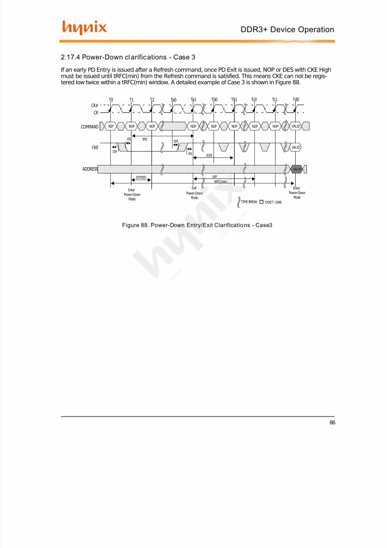
7/29/2019 DDR3 Device Operation Timing Diagram
http://slidepdf.com/reader/full/ddr3-device-operation-timing-diagram 86/154
86
DDR3+ Device Operation
2.17.4 Power-Down cl arifications - Case 3
If an early PD Entry is issued after a Refresh command, once PD Exit is issued, NOP or DES with CKE Highmust be issued until tRFC(min) from the Refresh command is satisfied. This means CKE can not be regis-
tered low twice within a tRFC(min) window. A detailed example of Case 3 is shown in Figure 88.
Figure 88. Power-Down Entry/Exit Clarificatio ns - Case3
T0 T1
CK CK#
CKE
T2 Ta0 Ta1 Tb0
tIS
DON’T CARETIME BREAK
NOPCOMMAND
tCPDED
ADDRESS
NOPREF
Tb1 Tc0
NOP NOPNOP
tIH tIS
tIH
tCKE
tXP
Enter Exit
Power-DownMode
Power-DownMode
EnterPower-Down
Mode
Tc1 Td0
VALIDNOP NOP
tPD
tRFC(min)
VALID
VALID
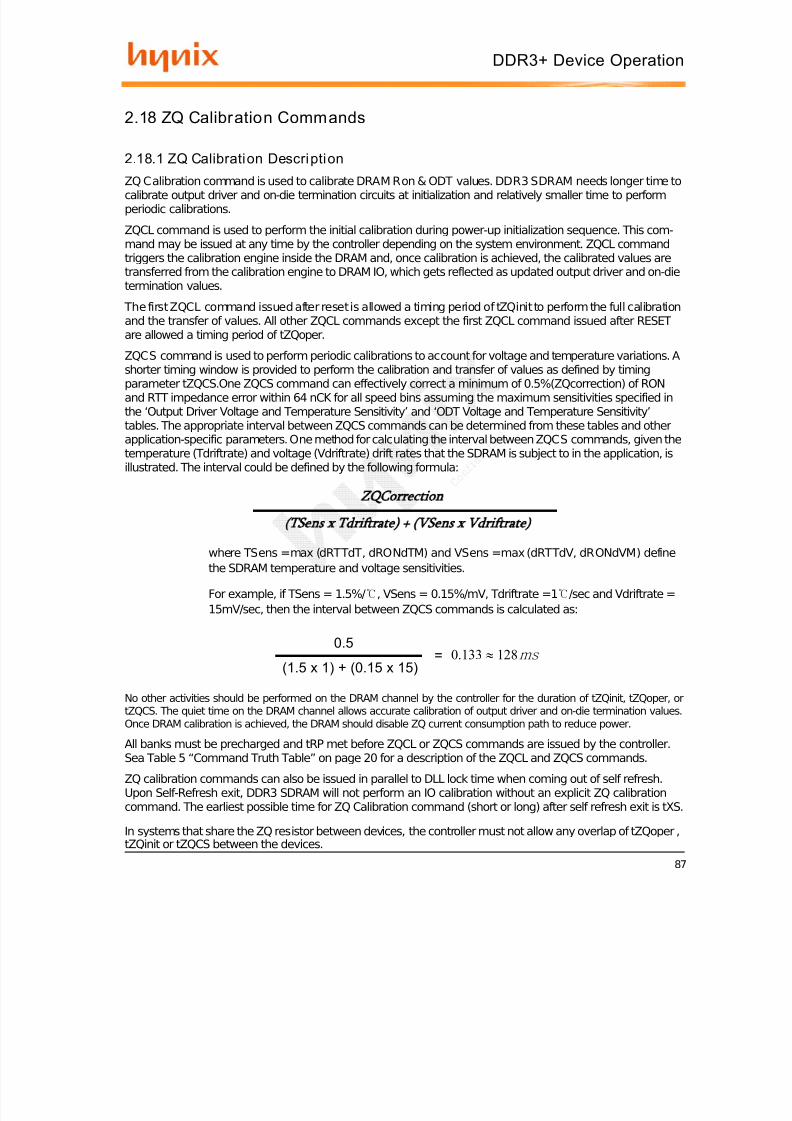
7/29/2019 DDR3 Device Operation Timing Diagram
http://slidepdf.com/reader/full/ddr3-device-operation-timing-diagram 87/154
87
DDR3+ Device Operation
2.18 ZQ Calibration Commands
2.18.1 ZQ Calibration Description
ZQ Calibration command is used to calibrate DRAM Ron & ODT values. DDR3 SDRAM needs longer time tocalibrate output driver and on-die termination circuits at initialization and relatively smaller time to performperiodic calibrations.
ZQCL command is used to perform the initial calibration during power-up initialization sequence. This com-mand may be issued at any time by the controller depending on the system environment. ZQCL commandtriggers the calibration engine inside the DRAM and, once calibration is achieved, the calibrated values aretransferred from the calibration engine to DRAM IO, which gets reflected as updated output driver and on-dietermination values.
The first ZQCL command issued after reset is allowed a timing period of tZQinit to perform the full calibrationand the transfer of values. All other ZQCL commands except the first ZQCL command issued after RESETare allowed a timing period of tZQoper.
ZQCS command is used to perform periodic calibrations to account for voltage and temperature variations. Ashorter timing window is provided to perform the calibration and transfer of values as defined by timingparameter tZQCS.One ZQCS command can effectively correct a minimum of 0.5%(ZQcorrection) of RONand RTT impedance error within 64 nCK for all speed bins assuming the maximum sensitivities specified inthe ‘Output Driver Voltage and Temperature Sensitivity’ and ‘ODT Voltage and Temperature Sensitivity’tables. The appropriate interval between ZQCS commands can be determined from these tables and otherapplication-specific parameters. One method for calculating the interval between ZQCS commands, given thetemperature (Tdriftrate) and voltage (Vdriftrate) drift rates that the SDRAM is subject to in the application, isillustrated. The interval could be defined by the following formula:
where TSens = max (dRTTdT, dRONdTM) and VSens =max (dRTTdV, dRONdVM) definethe SDRAM temperature and voltage sensitivities.
For example, if TSens = 1.5%/ , VSens = 0.15%/mV, Tdriftrate =1 /sec and Vdriftrate =15mV/sec, then the interval between ZQCS commands is calculated as:
No other activities should be performed on the DRAM channel by the controller for the duration of tZQinit, tZQoper, ortZQCS. The quiet time on the DRAM channel allows accurate calibration of output driver and on-die termination values.Once DRAM calibration is achieved, the DRAM should disable ZQ current consumption path to reduce power.
All banks must be precharged and tRP met before ZQCL or ZQCS commands are issued by the controller.Sea Table 5 “Command Truth Table” on page 20 for a description of the ZQCL and ZQCS commands.
ZQ calibration commands can also be issued in parallel to DLL lock time when coming out of self refresh.Upon Self-Refresh exit, DDR3 SDRAM will not perform an IO calibration without an explicit ZQ calibrationcommand. The earliest possible time for ZQ Calibration command (short or long) after self refresh exit is tXS.
In systems that share the ZQ resistor between devices, the controller must not allow any overlap of tZQoper ,tZQinit or tZQCS between the devices.
ZQCorrection
(TSens x Tdriftrate) + (VSens x Vd riftrate)
0.5
(1.5 x 1) + (0.15 x 15)= 0.133 128ms ≈
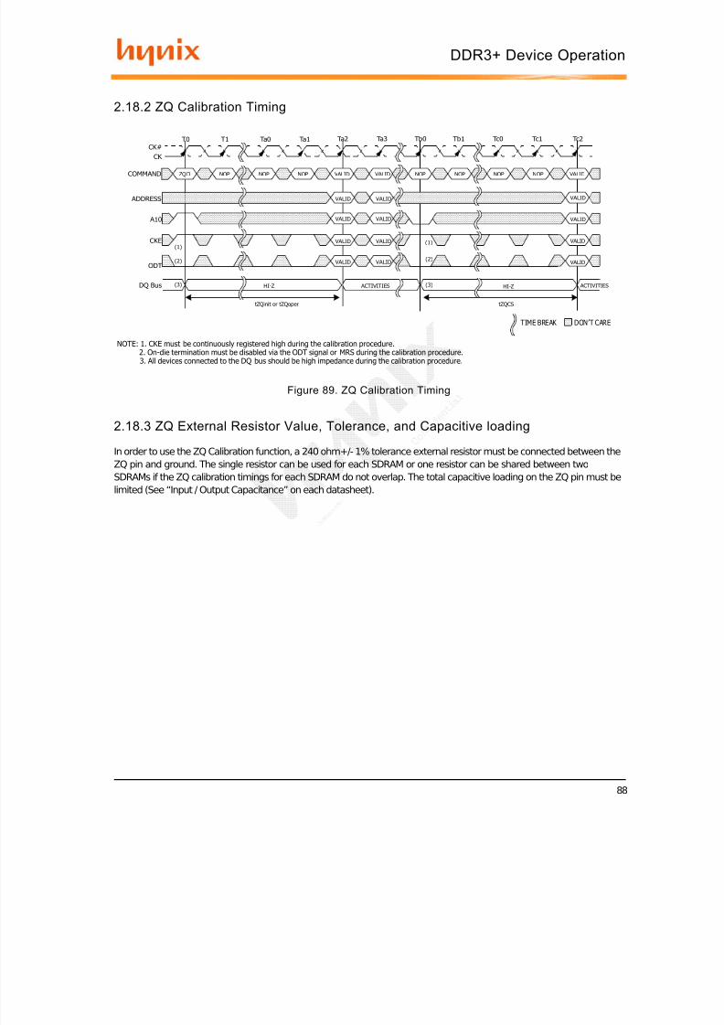
7/29/2019 DDR3 Device Operation Timing Diagram
http://slidepdf.com/reader/full/ddr3-device-operation-timing-diagram 88/154
88
DDR3+ Device Operation
2.18.2 ZQ Calibration Timing
Figure 89. ZQ Calibration Timing
2.18.3 ZQ External Resistor Value, Tolerance, and Capacitive loading
In order to use the ZQ Calibration function, a 240 ohm+/- 1% tolerance external resistor must be connected between theZQ pin and ground. The single resistor can be used for each SDRAM or one resistor can be shared between twoSDRAMs if the ZQ calibration timings for each SDRAM do not overlap. The total capacitive loading on the ZQ pin must belimited (See “Input / Output Capacitance” on each datasheet).
T0 T1
CK
CK#Ta0 Ta1 Ta2 Ta3 Tb0 Tb1 Tc0 Tc1 Tc2
CKE
ZQCL NOP NOP NOP VALID VALID NOP NOP NOP NOP VALIDCOMMAND
ADDRESS
(1)
VALID VALID
VALID VALID
VALID
VALID
VALID VALID VALID
ODT(2) VALID VALID VALID
A10
(1)
(2)
DQ Bus (3) HI-Z ACTIVITIES HI-Z(3) ACTIVITIES
tZQinit or tZQoper tZQCS
TIME BREAK DON’T CARE
NOTE: 1. CKE must be continuously registered high during the calibration procedure.2. On-die termination must be disabled via the ODT signal or MRS during the calibration procedure.3. All devices connected to the DQ bus should be high impedance during the calibration procedure.
7/29/2019 DDR3 Device Operation Timing Diagram
http://slidepdf.com/reader/full/ddr3-device-operation-timing-diagram 89/154
89
DDR3+ Device Operation
3. On-Die Term inat ion (ODT)
ODT (On-Die Termination) is a feature of the DDR3 SDRAM that allows the DRAM to turn on/off termination
resistance for each DQ, DQS, DQS and DM for x4 and x8 configuration (and TDQS, TDQS for X8 configura-tion, when enabled via A11=1 in MR1) via the ODT control pin. For x16 configuration , ODT is applied to eachDQU, DQL, DQSU, DQSU, DQSL, DQSL, DMU and DML signal via the ODT control pin. The ODT feature isdesigned to improve signal integrity of the memory channel by allowing the DRAM controller to independentlyturn on/off termination resistance for any or all DRAM devices. More details about ODT control modes andODT timing modes can be found further down in this document:• The ODT control modes are described in 3.1.• The ODT synchronous mode is described in 3.2.• The dynamic ODT feature is described in 3.3.• The ODT asynchronous mode is described in 3.4• The transitions between ODT synchronous and asynchronous are described in 3.4.1 through 3.4.4
The ODT feature is turned off and not supported in Self-Refresh mode.A simple functional representation of the DRAM ODT feature is shown in Figure 90.
Figure 90. Functi onal Representation of ODT
The switch is enabled by the internal ODT control logic, which uses the external ODT pin and other controlinformation, see below. The value of RTT is determined by the settings of Mode Register bits (see Figure 7on page 14 and Figure 8 on page 17 ). The ODT pin will be ignored if the Mode Register MR1 and MR2 are
programmed to disable ODT and in self-refresh mode.
3.1 ODT Mode Regis ter and ODT Truth Table The ODT Mode is enabled if either of MR1 A9, A6, A2or MR2 A10, A9are non zero. In this case , the valueof RTT is determined by the settings of those bits (see Figure 7 on page 14 ).Application: Controller sends WR command together with ODT asserted.• One possible application: The rank that is being written to provides termination.• DRAM turns ON termination if it sees ODT asserted (except ODT is disabled by MR).• DRAM does not use any write or read command decode information.• The Termination Truth Table is shown in Table 14.
ODT VDD Q/2
RTT
Switch
DQ, DQS, DM, TDQS
To othercircuitrylikeRCV, ...

7/29/2019 DDR3 Device Operation Timing Diagram
http://slidepdf.com/reader/full/ddr3-device-operation-timing-diagram 90/154
90
DDR3+ Device Operation
3.2 Synchronous ODT ModeSynchronous ODT mode is selected whenever the DLL is turned on and locked. Based on the power-downdefinition, these modes are:• Any bank active with CKE high• Refresh with CKE high• Idle mode with CKE high• Active power down mode (regardless of MR0 bit A12)
• Precharge power down mode if DLL is enabled during precharge power down by MR0 bit A12. The direct ODT feature is not supported during DLL-off mode. The on-die termination resistors must be dis-abled by continuously registering the ODT pin low and/or by programming the RTT_Nom bits MR1A9,A6,A2to 0,0,0via a mode register set command during DLL-off mode.
In synchronous ODT mode, RTT will be turned on ODTLon clock cycles after ODT is sampled high by a risingclock edge and turned off ODTLoff clock cycles after ODT is registered low by a rising clock edge. The ODTlatency is tied to the write latency (WL) by: ODTLon =WL - 2; ODTLoff =WL -2.
3.2.1 ODT Latency and Posted ODT
In Synchronous ODT Mode, the Additive Latency (AL) programmed into the Mode Register (MR1) alsoapplies to the ODT signal. The DRAM internal ODT signal is delayed for a number of clock cycles defined bythe Additive Latency (AL) relative to the external ODT signal. ODTLon =CWL +AL - 2;ODTLoff =CWL +AL - 2. For details, refer to ODT Timing Parameters listed in Table 41 on page 131 and
Table 42on page 138.
3.2.2 Timing Parameters
In synchronous ODT mode, the following timing parameters apply (see also Figure 91):
ODTLon, ODTLoff , tAON,min,max
, tAOF,min,max
.
Minimum RTT turn-on time ( tAONmin) is the point in time when the device leaves high impedance and ODTresistance begins to turn on. Maximum RTT turn on time ( tAONmax) is the point in time when the ODTresistance is fully on. Both are measured from ODTLon.Minimum RTT turn-off time ( tAOFmin) is the point in time when the device starts to turn off the ODT resistance.Maximum RTT turn off time ( tAOFmax) is the point in time when the on-die termination has reached highimpedance. Both are measured from ODTLoff.
When ODT is asserted, it must remain high until ODTH4 is satisfied. If a Write command is registered by theSDRAM with ODT high, then ODT must remain high until ODTH4 (BL =4) or ODTH8 (BL =8) after the Writecommand (see Figure 92). ODTH4 and ODTH8 are measured from ODT registered high to ODT registeredlow or from the registration of a Write command until ODT is registered low.
Table 14. Termin ation Truth Table
ODT pin DRAM Termination State
0 OFF1 On, (OFF, if disabled by MR1 A9, A6, A2and MR2 A10, A9in general)

7/29/2019 DDR3 Device Operation Timing Diagram
http://slidepdf.com/reader/full/ddr3-device-operation-timing-diagram 91/154
91
DDR3+ Device Operation
Figure 91. Synchronous ODT Timing Example for AL=3; CWL=5; ODTLon = AL+CWL-2=6.0;ODTLof f = AL +CWL-2=6
Figure 92. Synchronou s ODT example wi th B L=4, WL=7
T0 T1
CK CK#
CKE
T2 T3 T4 T5
DRAM_RTT
T6 T7
AL=3
ODTH4, min
tAONmin
T8 T9 T10 T11 T12 T13 T14 T15
AL=3 CWL-2
ODT
ODTLon = CWL+AL-2
ODTLoff = CWL+AL-2
tAONmax
RTT_NOM
tAOFmax
tAOFmin
TRANSITIONING DON’’T CARE
T0 T1
CK CK#
CKE
T2 T3 T4 T5
DRAM_RTT
T6 T7
tAONmin
T8 T9 T10 T11 T12 T13 T14 T15
ODTH4min
ODTH4
ODT
ODTLoff = WL-2
tAONmax
RTT_NOM
tAOFmax
tAOFmin
T16 T17
NOP NOP NOP NOP NOP NOP NOP WRS4 NOP NOP NOP NOP NOP NOP NOP NOP NOP NOP
ODTH4
ODTLoff = WL-2
ODTLon = WL-2 ODTLon = WL-2
COMMAND
tAOFmax
tAONmin
tAONmaxtAOFmin
TRANSITIONING DON’T CARE

7/29/2019 DDR3 Device Operation Timing Diagram
http://slidepdf.com/reader/full/ddr3-device-operation-timing-diagram 92/154
92
DDR3+ Device Operation
ODT must be held high for at least ODTH4 after assertion (T1); ODT must be kept high ODTH4 (BL = 4) orODTH8 (BL = 8) after Write command (T7). ODTH is measured from ODT first registered high to ODT firstregistered low, or from registration of Write command with ODT high to ODT registered low. Note thatalthough ODTH4 is satisfied from ODT registered high at T6, ODT must not go low before T11 as ODTH4
must also be satisfied from the registration of the Write command at T7.
3.2.3 ODT dur ing Reads
As the DDR3 SDRAM can not terminate and drive at the same time, RTT must be disabled at least half aclock cycle before the read preamble by driving the ODT pin low appropriately. RTT may not be enabled untilthe end of the post-amble as shown in the example below. As shown in Figure 93 below at cycle T15, DRAMturns on the termination when it stops driving, which is determined by tHZ. If DRAM stops driving early (i.e.,tHZ is early), then tAONmin timing may apply. If DRAM stops driving late (i.e., tHZ is late), then DRAM com-plies with tAONmax timing. Note that ODT may be disabled earlier before the Read and enabled later afterthe Read than shown in this example in Figure 93.
Figure 93. ODT must be di sabled externally dur ing Reads by drivi ng ODT low. (example: CL=6; AL =CL-1=5; RL=A L+CL=11; CWL=5; ODTLon = CWL+A L-2=8; ODTLoff = CWL+AL -2=8)
T0 T1
CK CK#
T2 T3 T4 T5
DQS,DQS#
T6 T7
tAOFmin
T8 T9 T10 T11 T12 T13 T14 T15
ODTLon = CWL+AL-2
ODT
RTT_NOM
tAONmax
T16 T17
READ NOP NOP NOP NOP NOP NOP NOP NOP NOP NOP NOP NOP NOP NOP NOP NOP NOP
ODTLoff = CWL+AL-2
COMMAND
TRANSITIONING DON’T CARE
ADDRESS VALID
RTT RTT_NOM
DINb DINb+1 DINb+2 DINb+3 DINb+4 DINb+5 DINb+6 DINb+7DQ
RL=AL+CL
tAOFmax

7/29/2019 DDR3 Device Operation Timing Diagram
http://slidepdf.com/reader/full/ddr3-device-operation-timing-diagram 93/154
93
DDR3+ Device Operation
3.3 Dynamic ODT
In certain application cases and to further enhance signal integrity on the data bus, it is desirable that the ter-mination strength of the DDR3 SDRAM can be changed without issuing an MRS command. This requirement
is supported by the “Dynamic ODT” feature as described as follows:
3.3.1 Funct ional Descrip tion: The Dynamic ODT Mode is enabled if bit (A9) or (A10) of MR2 is set to ’1’. The function is described as follows:• Two RTT values are available: RTT_Nom and RTT_WR.
– The value for RTT_Nom is preselected via bits A[9,6,2] in MR1 .– The value for RTT_WR is preselected via bits A[10,9] in MR2 .
• During operation without write commands, the termination is controlled as follows:– Nominal termination strength RTT_Nom is selected.– Termination on/off timing is controlled via ODT pin and latencies ODTLon and ODTLoff.
• When a write command (WR, WRA, WRS4, WRS8, WRAS4, WRAS8) is registered, and if Dynamic ODT
is enabled, the termination is controlled as follows:– A latency ODTLcnw after the write command, termination strength RTT_WR is selected.– A latency ODTLcwn8 (for BL8, fixed by MRS or selected OTF) or ODTLcwn4 (for BC4, fixed by MRS or
selected OTF) after the write command, termination strength RTT_Nom is selected.– Termination on/off timing is controlled via ODT pin and ODTLon, ODTLoff.
Table 16 shows latencies and timing parameters which are relevant for the on-die termination control inDynamic ODT mode.
The dynamic ODT feature is not supported at DLL-off mode. User must use MRS command to set Rtt_WR,MR2A10, A9=0,0, to disable Dynamic ODT externally.
When ODT is asserted, it must remain high until ODTH4 is satisfied. If a Write command is registered by theSDRAM with ODT high, then ODT must remain high until ODTH4 (BL =4) or ODTH8 (BL =8) after the Writecommand (see Figure 92). ODTH4 and ODTH8 are measured from ODT registered high to ODT registeredlow or from the registration of a Write command until ODT is registered low.
Table 15. Latencies and ti ming parameters relevant fo r Dynamic ODT
Name andDescription Ab br . Defined
From Defined t o Definiti on fo r all DDR3speed bins Unit
ODT turn-on Latency ODTLonregisteringexternal ODTsignal high
turning terminationon ODTLon = WL - 2 tCK
ODT turn-off Latency ODTLoff registeringexternal ODTsignal low
turning terminationoff ODTLoff = WL - 2 tCK
ODT Latency forchanging from
RTT_Nom to RTT_WRODTLcnw
registeringexternal writecommand
change RTT strengthfrom RTT_Nom toRTT_WR
ODTLcnw = WL - 2 tCK
ODT Latency for changefrom RTT_WR toRTT_Nom(BL=4)
ODTLcwn4registeringexternal writecommand
change RTT strengthfrom RTT_WR toRTT_Nom
ODTLcwn4=
4+ODTLoff tCK
ODT Latency for changefrom RTT_WR toRTT_Nom(BL=8)
ODTLcwn8registeringexternal writecommand
change RTT strengthfrom RTT_WR toRTT_Nom
ODTLcwn8=
6+ODTLoff tCK (avg)
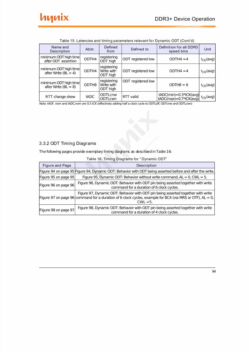
7/29/2019 DDR3 Device Operation Timing Diagram
http://slidepdf.com/reader/full/ddr3-device-operation-timing-diagram 94/154
94
DDR3+ Device Operation
3.3.2 ODT Timing Diagrams
The following pages provide exemplary timing diagrams as described in Table 16:
Table 15. Latencies and timin g parameters relevant fo r Dynamic ODT (Cont’d)
Note: tAOF, nom and tADC,nom are 0.5 tCK (effectively adding half a clock cycle to ODTLoff, ODTcnw and ODTLcwn)
Name andDescription Ab br . Defined
from Defined to Definit ion f or all DDR3speed bins Unit
minimum ODT high timeafter ODT assertion ODTH4 registering
ODT high ODT registered low ODTH4 = 4 tCK (avg)
minimum ODT high timeafter Write (BL = 4) ODTH4
registeringWrite withODT high
ODT registered low ODTH4 = 4 tCK (avg)
minimum ODT high timeafter Write (BL = 8) ODTH8
registeringWrite withODT high
ODT registered lowODTH8 = 6 tCK (avg)
RTT change skew tADC ODTLcnwODTLcwn RTT valid tADC(min)=0.3*tCK(avg)
tADC(max)=0.7*tCK(avg) tCK (avg)
Table 16. Timin g Diagrams for “ Dynamic ODT”
Figure and Page Description
Figure 94 on page 95 Figure 94, Dynamic ODT: Behavior with ODT being asserted before and after the write.Figure 95 on page 95 Figure 95, Dynamic ODT: Behavior without write command, AL = 0, CWL = 5.
Figure 96 on page 96 Figure 96, Dynamic ODT: Behavior with ODT pin being asserted together with writecommand for a duration of 6 clock cycles.
Figure 97 on page 96Figure 97, Dynamic ODT: Behavior with ODT pin being asserted together with write
command for a duration of 6 clock cycles, example for BC4 (via MRS or OTF), AL = 0,CWL =5.
Figure 98 on page 97 Figure 98, Dynamic ODT: Behavior with ODT pin being asserted together with writecommand for a duration of 4 clock cycles.
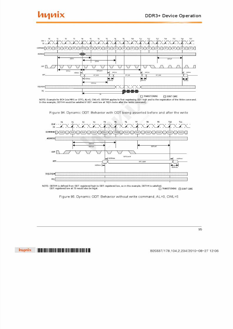
7/29/2019 DDR3 Device Operation Timing Diagram
http://slidepdf.com/reader/full/ddr3-device-operation-timing-diagram 95/154

7/29/2019 DDR3 Device Operation Timing Diagram
http://slidepdf.com/reader/full/ddr3-device-operation-timing-diagram 96/154

7/29/2019 DDR3 Device Operation Timing Diagram
http://slidepdf.com/reader/full/ddr3-device-operation-timing-diagram 97/154
97
DDR3+ Device Operation
Figure 98. Dynamic ODT: Behavior wi th ODT pin being asserted together wi th wr ite command f or aduration of 4 clock cycles
T0 T1
CK CK#
T2 T3 T4 T5
DQS,DQS#
T6 T7
tADCmax
T8 T9 T10 T11
ODTLoff
ODT
NOP WRS4 NOP NOP NOP NOP NOP NOP NOP NOP NOP NOP
ODTH4
COMMAND
ADDRESS
RTT
DINb
DINb+1
DINb+2
DINb+3
DQ
ODTLcwn4tAONmin
VALID
ODTLcnw
RTT_WR
WL
ODTLon tAOFmin
tAOFmax
TRANSITIONING DON’T CARENOTE: Example for BC4 (via MRS or OTF), AL=0, CWL=5. In this example, ODTH=4 is exactly satisfied.

7/29/2019 DDR3 Device Operation Timing Diagram
http://slidepdf.com/reader/full/ddr3-device-operation-timing-diagram 98/154
98
DDR3+ Device Operation
3.4 Asynchronous ODT ModeAsynchronous ODT mode is selected when DRAM runs in DLLon mode, but DLL is temporarily disabled (i.e.frozen) in precharge power-down (by MR0 bit A12). Based on the power down mode definitions, this iscurrently (comment: update editorially after everything is set and done...): Precharge power down mode if DLLis disabled during precharge power down by MR0 bit A12.In asynchronous ODT timing mode, internal ODT command is NOT delayed by Additive Latency (AL) relativeto the external ODT command.In asynchronous ODT mode, the following timing parameters apply (see Figure 99): tAONPD,min,max ,tAOFPD,min,max .Minimum RTT turn-on time ( tAONPDmin) is the point in time when the device termination circuit leaves highimpedance state and ODT resistance begins to turn on. Maximum RTT turn on time ( tAONPDmax) is the pointin time when the ODT resistance is fully on.tAONPDmin and t AONPDmax are measured from ODT being sampled high.
Minimum RTT turn-off time ( tAOFPDmin) is the point in time when the devices termination circuit starts to turn
off the ODT resistance. Maximum ODT turn off time ( tAOFPDmax) is the point in time when the on-die termina-tion has reached high impedance. t AOFPDmin and t AOFPDmax are measured from ODT being sampled low.
Figure 99. Async hron ous ODT Timing s on DDR3 SDRAM with fast ODT transiti on: A L is ignor ed
In Precharge Power Down, ODT receiver remains active, however no Read or Write command can be issued,as the respective ADD/CMD receivers may be disabled.
T0 T1
CK CK#
CKE
T2 T3 T4 T5
RTT
T6 T7
tAONPD min
T8 T9 T10 T11 T12 T13 T14 T15
ODT
tAONPDmax
T16 T17
TRANSITIONING DON’T CARE
tIH tIS tIH tIS
tAOFPDmin
tAOFPDmax
RTT
Table 17. Asynchr onous ODT Timings Parameters for all Speed Bins
Symbol Description min max Unit
tAONPD Asynchronous RTT turn-on delay (Power-Down with DLL frozen) 2 8.5 ns
tAOFPD Asynchronous RTT turn-off delay (Power-Down with DLL frozen) 2 8.5 ns

7/29/2019 DDR3 Device Operation Timing Diagram
http://slidepdf.com/reader/full/ddr3-device-operation-timing-diagram 99/154
99
DDR3+ Device Operation
3.4.1 Synchronous to Asynchronous ODT Mode Transit ions
3.4.2 Synchronous to Asynchronous ODT Mode Transit ion during Power-DownEntry
If DLL is selected to be frozen in Precharge Power Down Mode by the setting of bit A12 in MR0 to “0”, there isa transition period around power down entry, where the DDR3 SDRAM may show either synchronous orasynchronous ODT behavior.
The transition period is defined by the parameters tANPD and tCPDED(min). tANPD is equal to (WL-1) and iscounted backwards in time from the clock cycle where CKE is first registered low. tCPDED(min) starts with theclock cycle where CKE is first registered low. The transition period begins with the starting point of tANPD andterminates at the end point of tCPDED(min) as shown in Figure 83. If there is a Refresh command in progresswhile CKE goes low, then the transition period ends at the later one of tRFC(min) after the Refresh commandand the end point of tCPDED (min) as shown in Figure 84. Please note that the actual starting point at tANPDis excluded from the transition period, and the actual end points at tCPDED(min) and tRFC(min), respectively,
are included in the transition period.ODT assertion during the transition period may result in an RTT change as early as the smaller of t AONPDminand (ODTLon*t CK +t AONmin) and as late as the larger of t AONPDmax and(ODTLon*t CK + t AONmax). ODT de-assertion during the transition period may result in an RTT change asearly as the smaller of t AOFPDmin and (ODTLof*t CK + t AOFmin) and as late as the larger of t AOFPDmax and(ODTLoff*t CK + t AOFmax). See Figure 16 and Figure 100. Note that, if AL has a large value, the range whereRTT is uncertain becomes quite large. Figure 100 shows the three different cases: ODT_A, synchronousbehavior before tANPD; ODT_B has a state change during the transition period; ODT_C shows a statechange after the transition period.
Table 18. ODT timing parameters fo r Power Down (with DLL frozen) entry and exit tr ansition period
Description min max
ODT to RTTturn-on delay
min ODTLon * tCK +tAONmin; tAONPDmin max ODTLon * tCK +tAONmax; tAONPDmaxmin (WL-2) * tCK +tAONmin; tAONPDmin min (WL-2) * tCK +tAONmax; tAONPDmax
ODT to RTTturn-off delay
min ODTLoff * tCK +tAOFmin; tAOFPDmin min ODTLoff * tCK +tAOFmax; tAOFPDmax
min (WL-2) * tCK +tAOFmin; tAOFPDmin min (WL-2) * tCK +tAOFmax; tAOFPDmax
tANPD WL-1
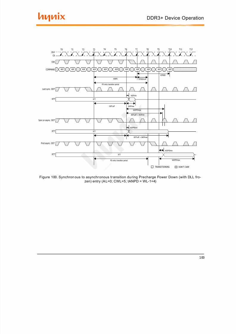
7/29/2019 DDR3 Device Operation Timing Diagram
http://slidepdf.com/reader/full/ddr3-device-operation-timing-diagram 100/154
100
DDR3+ Device Operation
Figure 100. Synchron ous to asynchr onous tr ansition du ring Precharge Power Down (with DLL fro-zen) entry (A L=0; CWL=5; tANPD = WL-1=4)
T0 T1
CK CK#
CKE
T2 T3 T4 T5
First async. ODT
T6 T7
tANPD
T8 T9 T10 T11 T12
tCPDED
TRANSITIONING DON’T CARE
NOP NOP NOP NOP NOP NOP NOP NOP NOP NOP NOPCOMMAND
tCPDEDmin
PD entry transition period
Last sync. ODT
RTT
tAOFmin
tAOFmax
tAOFPDmax
Sync or async. ODT
RTT
ODTLoff + tAOFmin
RTT
tAOFPDmin
ODTLoff + tAOFmax
RTT
RTT
tAOFPDmin
PD entry transition period
RTT
tAOFPDmax
ODTLoff
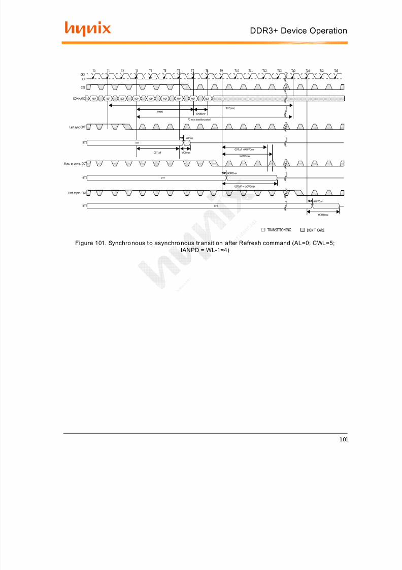
7/29/2019 DDR3 Device Operation Timing Diagram
http://slidepdf.com/reader/full/ddr3-device-operation-timing-diagram 101/154
101
DDR3+ Device Operation
Figure 101. Synchro nous t o asynchro nous tr ansition after Refresh command (AL=0; CWL=5;tANPD = WL-1=4)
T0 T1
CK CK#
T2 T3 T4 T5
Sync, or async. ODT
T6 T7 T8 T9 T10 T11 T12 T13 Ta0 Ta1
Last sync.ODT
Ta2 Ta3
NOP REF NOP NOP NOP NOP NOP NOP NOPCOMMAND
TRANSITIONING DON’T CARE
RTTtAOFmin
tAOFmax
CKE
tRFC(min)tANPD
tCPDEDmin
PD entry transition period
RTT
ODTLoff ODTLoff + tAOFPDmin
tAOFPDmax
tAOFPDmin
RTT
ODTLoff + tAOFPDmax
RTT
tAOFPDmin
RTT
tAOFPDmax
RTT
First async. ODT
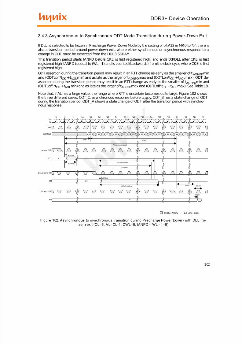
7/29/2019 DDR3 Device Operation Timing Diagram
http://slidepdf.com/reader/full/ddr3-device-operation-timing-diagram 102/154
102
DDR3+ Device Operation
3.4.3 Asynchronous to Synchronous ODT Mode Transit ion during Power-Down Exit
If DLL is selected to be frozen in Precharge Power Down Mode by the setting of bit A12 in MR0 to “0”, there isalso a transition period around power down exit, where either synchronous or asynchronous response to achange in ODT must be expected from the DDR3 SDRAM.
This transition period starts tANPD before CKE is first registered high, and ends tXPDLL after CKE is firstregistered high. tANPD is equal to (WL - 1) and is counted (backwards) from the clock cycle where CKE is firstregistered high.ODT assertion during the transition period may result in an RTT change as early as the smaller of t AONPDminand (ODTLon*t CK +t AONmin) and as late as the larger of t AONPDmax and (ODTLon*t CK +t AONmax). ODT de-assertion during the transition period may result in an RTT change as early as the smaller of t AOFPDmin and(ODTLoff *t CK +t AOFmin) and as late as the larger of t AOFPDmax and (ODTLoff*t CK +t AOFmax). See Table 18.
Note that, if AL has a large value, the range where RTT is uncertain becomes quite large. Figure 102 showsthe three different cases: ODT_C, asynchronous response before t ANPD; ODT_B has a state change of ODTduring the transition period; ODT_A shows a state change of ODT after the transition period with synchro-
nous response.
Figure 102. Async hrono us to sync hrono us transiti on duri ng Precharge Power Down (with DLL fro-zen) exit (CL=6; AL=CL-1; CWL=5; tANPD = WL - 1=9)
T0 T1
CK CK#
T2 Ta0 Ta1 Ta2
Sync, or async. ODT
Ta3 Ta4 Ta5 Ta6 Tb0 Tb1 Tb2 Tc0 Tc1 Tc2
Last sync. ODT
Td0 Td1
NOP NOP NOP NOPNOP NOP NOP NOP NOPCOMMAND
RTT
tAOFPDmin
tAOFPDmax
CKE
tANPD tXPDLL
PD entry transition period
RTT
ODTLoff + tAOFmin
tAOFPDmax
tAOFPDmin
RTT
ODTLoff + tAOFmax
RTT
tAOFmin
RTT
tAOFmax
RTT
First async. ODT
NOP NOPNOP NOPNOP
ODTLoff
TRANSITIONING DON’T CARE
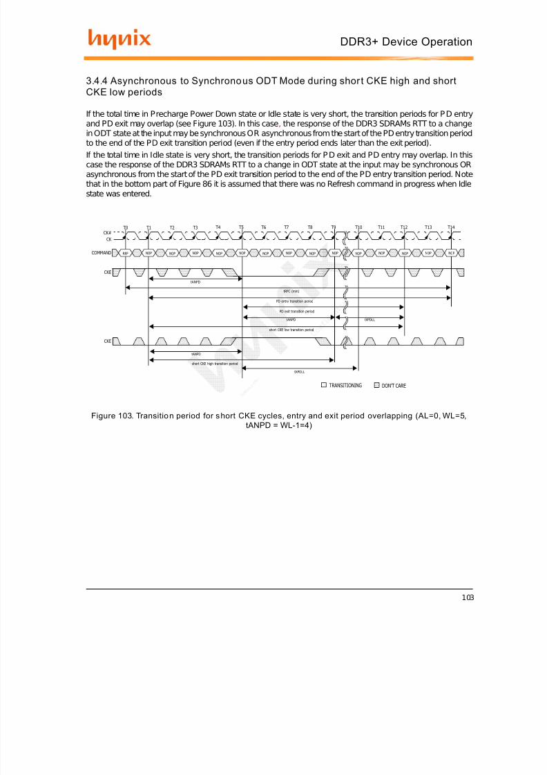
7/29/2019 DDR3 Device Operation Timing Diagram
http://slidepdf.com/reader/full/ddr3-device-operation-timing-diagram 103/154
103
DDR3+ Device Operation
3.4.4 Asynchronous to Synchronous ODT Mode during shor t CKE high and shortCKE low periods
If the total time in Precharge Power Down state or Idle state is very short, the transition periods for P D entryand PD exit may overlap (see Figure 103). In this case , the response of the DDR3 SDRAMs RTT to a changein ODT state at the input may be synchronous OR asynchronous from the start of the PD entry transition periodto the end of the PD exit transition period (even if the entry period ends later than the exit period).If the total time in Idle state is very short, the transition periods for P D exit and PD entry may overlap. In thiscase the response of the DDR3 SDRAMs RTT to a change in ODT state at the input may be synchronous ORasynchronous from the start of the PD exit transition period to the end of the PD entry transition period. Notethat in the bottom part of Figure 86 it is assumed that there was no Refresh command in progress when Idlestate was entered.
Figure 103. Transitio n period for s hort CKE cycles, entry and exit period overlapping (AL=0, WL=5,tANPD = WL-1=4)
T0 T1
CK
CK#T2 T3 T4 T5 T6 T7
tANPD
T8 T9 T10 T11 T12 T13 T14
CKE
TRANSITIONING DON’T CARE
REF NOPCOMMAND NOP NOP NOP NOP NOP NOP NOP NOP NOP NOP NOP NOP NOP
CKE
tRFC (min)
PD entry transition period
PD exit transition period
tANPD tXPDLL
short CKE low transition period
tANPD
short CKE high transition period
tXPDLL
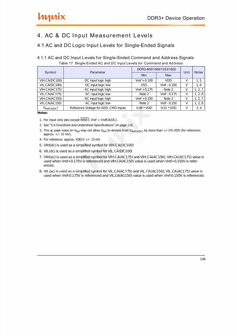
7/29/2019 DDR3 Device Operation Timing Diagram
http://slidepdf.com/reader/full/ddr3-device-operation-timing-diagram 104/154
104
DDR3+ Device Operation
4 . AC & DC Inpu t Measu remen t Leve l s
4.1 AC and DC Logic Input Levels for Single-Ended Signals
4.1.1 AC and DC Input Levels for Sing le-Ended Command and Address Signals
Table 17. Single-Ended AC and DC Input Levels for Command and Ad dress
Symbol Parameter DDR3-800/1066/1333/1600
Unit NotesMin Max
VIH.CA(DC100) DC input logic high Vref +0.100 VDD V 1, 5VIL.CA(DC100) DC input logic low VSS Vref - 0.100 V 1, 6VIH.CA(AC175) AC input logic high Vref +0.175 Note 2 V 1, 2, 7VIL.CA(AC175) AC input logic low Note 2 Vref - 0.175 V 1, 2, 8VIH.CA(AC150) AC input logic high Vref +0.150 Note 2 V 1, 2, 7
VIL.CA(AC150) AC input logic low Note 2 Vref - 0.150 V 1, 2, 8VRefCA(DC ) Reference Voltage for ADD, CMD inputs 0.49 * VDD 0.51 * VDD V 3, 4
Notes:
1. For input only pins except RESET, Vref = VrefCA(DC).
2. See “5.6 Overshoot and Undershoot Specifications” on page 116 .
3. The ac peak noise on V Ref may not allow V Ref to deviate from V RefCA(DC) by more than +/-1% VDD (for reference:approx. +/- 15 mV).
4. For reference: approx. VDD/2 +/- 15 mV.
5. VIH(dc) is used as a simplified symbol for VIH.CA(DC100)
6. VIL(dc) is used as a simplified symbol for VIL.CA(DC100)
7. VIH(ac) is used as a simplified symbol for VIH.CA(AC175) and VIH.CA(AC150); VIH.CA(AC175) value isused when Vref+0.175V is referenced and VIH.CA(AC150) value is used when Vref+0.150V is refer-enced.
8. VIL(ac) is used as a simplified symbol for VIL.CA(AC175) and VIL.CA(AC150); VIL.CA(AC175) value isused when Vref-0.175V is referenced and VIL.CA(AC150) value is used when Vref-0.150V is referenced.

7/29/2019 DDR3 Device Operation Timing Diagram
http://slidepdf.com/reader/full/ddr3-device-operation-timing-diagram 105/154
105
DDR3+ Device Operation
4.1.2 AC and DC Input Levels fo r Single-Ended Data Signals
DDR3 SDRAM will support two Vih/Vil AC levels for DDR3-800 and DDR3-1066 as specified in Table 24.DDR3 SDRAM will also support corresponding tDS values (Table 41on page 131 and Table 49on page 148 )
as well as derating tables Table 44on page 148 depending on Vih/Vil AC levels.Table 18. Single-Ended AC and DC Input Levels for DQ and DM
Symbol Parameter DDR3-800/1066 DDR3-1333/1600
Unit NotesMin Max Min Max
VIH.DQ(DC100)DC input logic high Vref +0.100 VDD Vref +0.100 VDD V 1, 5VIL.DQ(DC100) DC input logic low VSS Vref - 0.100 VSS Vref - 0.100 V 1, 6VIH.DQ(AC175) AC input logic high Vref +0.175 Note 2 - - V 1, 2, 7VIL.DQ(AC175) AC input logic low Note 2 Vref - 0.175 - - V 1, 2, 8VIH.DQ(AC150) AC Input logic high Vref +0.150 Note 2 Vref +0.150 Note 2 V 1, 2, 7VIL.DQ(AC150) AC input logic low Note 2 Vref - 0.150 Note 2 Vref - 0.150 V 1, 2, 8VIH.DQ(AC135) AC Input logic high - - - - mV 1, 2, 7VIL.DQ(AC135) AC input logic low - - - - mV 1, 2, 8
VRefDQ(DC ) Reference Voltagefor DQ, DM inputs 0.49 * VDD 0.51 * VDD 0.49 * VDD 0.51 * VDD V 3, 4
Notes:
1. Vref = VrefDQ(DC).
2. See “5.6 Overshoot and Undershoot Specifications” on page 116 .
3. The ac peak noise on V Ref may not allow V Ref to deviate from V RefDQ(DC) by more than +/-1% VDD (for reference:approx. +/- 15 mV).
4. For reference: approx. VDD/2 +/- 15 mV.
5. VIH(dc) is used as a simplified symbol for VIH.DQ(DC100)
6. VIL(dc) is used as a simplified symbol for VIL.DQ(DC100)
7. VIH(ac) is used as a simplified symbol for VIH.DQ(AC175), VIH.DQ(AC150), and VIH.DQ(AC135);VIH.DQ(AC175) value is used when Vref+0.175V is referenced, VIH.DQ(AC150) value is used whenVref+0.150V is referenced, and VIH.DQ(AC135) value is used when Vref+0.135V is referenced.
8. VIL(ac) is used as a simplified symbol for VIL.DQ(AC175), VIL.DQ(AC150), and VIL.DQ(AC135);VIL.DQ(AC175) value is used when Vref-0.175V is referenced, VIL.DQ(AC150) value is used when Vref-0.150V is referenced, and VIL.DQ(AC135) value is used when Vref-0.135V is referenced

7/29/2019 DDR3 Device Operation Timing Diagram
http://slidepdf.com/reader/full/ddr3-device-operation-timing-diagram 106/154
106
DDR3+ Device Operation
4.2 Vref Tolerances
The dc-tolerance limits and ac-noise limits for the reference voltages VRefCA and V RefDQ are illustrated inbelow Figure 104. It shows a valid reference voltage V Ref (t) as a function of time. (V Ref stands for V RefCA andVRefDQ likewise).VRef (DC) is the linear average of V Ref (t) over a very long period of time (e.g., 1 sec). This average has tomeet the min/max requirements in Table 23. Furthermore V Ref (t) may temporarily deviate from V Ref (DC) byno more than +/- 1% VDD.
Figure 104. Illustration o f V Ref(DC) tolerance and V Ref ac-noise limits
The voltage levels for setup and hold time measurements V IH(AC), V IH(DC) , V IL(AC), and V IL(DC) are dependenton V Ref .“VRef ” shall be understood as V Ref(DC) , as defined in Figure 104.
This clarifies that dc-variations of V Ref affect the absolute voltage a signal has to reach to achieve a valid highor low level and therefore the time to which setup and hold is measured. System timing and voltage budgetsneed to account for V Ref(DC) deviations from the optimum position within the data-eye of the input signals.
This also clarifies that the DRAM setup/hold specification and derating values need to include time and volt-age associated with V Ref ac-noise. Timing and voltage effects due to ac-noise on V Ref up to the specified limit
(+/- 1% of VDD) are included in DRAM timings and their associated deratings.
VDD
VSS
VDD/2VRef(DC)
VRef ac-noise
voltage
time
VRef(DC)max
VRef(DC)min
VRef (t)
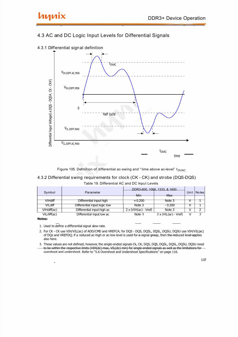
7/29/2019 DDR3 Device Operation Timing Diagram
http://slidepdf.com/reader/full/ddr3-device-operation-timing-diagram 107/154
107
DDR3+ Device Operation
4.3 AC and DC Logic Input Levels for Differential Signals
4.3.1 Differential signal definit ion
Figure 105. Definit ion of differential ac-swing and “ time above ac-level” t DVAC
4.3.2 Differential swing requirements for clock (CK - CK) and strobe (DQS-DQS)
time
D i f f e
r e n
t i a l I n
p u
t V
o l t a
g e
( i . e
. D Q S
- D Q S #
, C K
- C K # )
VIL.DIFF.AC.MAX
VIL.DIFF.MAX
0
VIH.DIFF.MIN
VIH.DIFF.AC.MIN
tDVAC
half cycle
tDVAC
Table 19. Differential AC and DC Inpu t Levels
Symbol Parameter DDR3-800, 1066, 1333, & 1600
Uni t No tesMin Max
VIHdiff Differential input high +0.200 Note 3 V 1VILdiff Differential input logic low Note 3 - 0.200 V 1
VIHdiff(ac) Differential input high ac 2 x (VIH(ac) - Vref) Note 3 V 2VILdiff(ac) Differential input low ac Note 3 2 x (VIL(ac) - Vref) V 2
Notes:
1. Used to define a differential signal slew-rate.
2. For CK - CK use VIH/VIL(ac) of ADD/CMD and VREFCA; for DQS - DQS, DQSL, DQSL, DQSU, DQSU use VIH/VIL(ac)of DQs and VREFDQ; if a reduced ac-high or ac-low level is used for a signal group, then the reduced level appliesalso here.
3. These values are not defined; however, the single-ended signals Ck, CK, DQS, DQS, DQSL, DQSL, DQSU, DQSU needto be within the respective limits (VIH(dc) max, VIL(dc) min) for single-ended signals as well as the limitations forovershoot and undershoot. Refer to “5.6 Overshoot and Undershoot Specifications” on page 116.

7/29/2019 DDR3 Device Operation Timing Diagram
http://slidepdf.com/reader/full/ddr3-device-operation-timing-diagram 108/154
108
DDR3+ Device Operation
4.3.3 Single-ended requirements for d ifferential signals
Each individual component of a differential signal (CK, DQS, DQSL, DQSU, CK, DQS, DQSL, of DQSU) hasalso to comply with certain requirements for single-ended signals.
CK and CK have to approximately reach VSEHmin / VSELmax (approximately equal to the ac-levels (VIH(ac) / VIL (ac) for ADD/CMD signals) in every half-cycle.
DQS, DQSL, DQSU, DQS, DQSL have to reach VSEHmin / VSELmax (approximately the ac-levels (VIH (ac)/ VIL (ac)) for DQ signals) in every half-cycle preceding and following a valid transition.
Note that the applicable ac-levels for ADD/CMD and DQ’s might be different per speed-bin etc. E.g., if VIH.CA(AC150)/VIL.CA(AC150) is used for ADD/CMD signals, then these ac-levels apply also for the single-ended signals CK and CK.
Table 20. All owed ti me befor e ringback (tDVAC) for CK - CK and DQS - DQS
Slew Rate [V/ns]tDVAC [ps]
@ |VIH/Ldiff(ac)| = 350mVtDVAC [ps ]
@ |VIH/Ldiff(ac)| = 300mV
min max min max
>4.0 75 - 175 -4.0 57 - 170 -3.0 50 - 167 -2.0 38 - 1631.8 34 - 162 -1.6 29 - 161 -1.4 22 - 159 -1.2 13 - 155 -
1.0 0 - 150 -<1.0 0 - 150 -
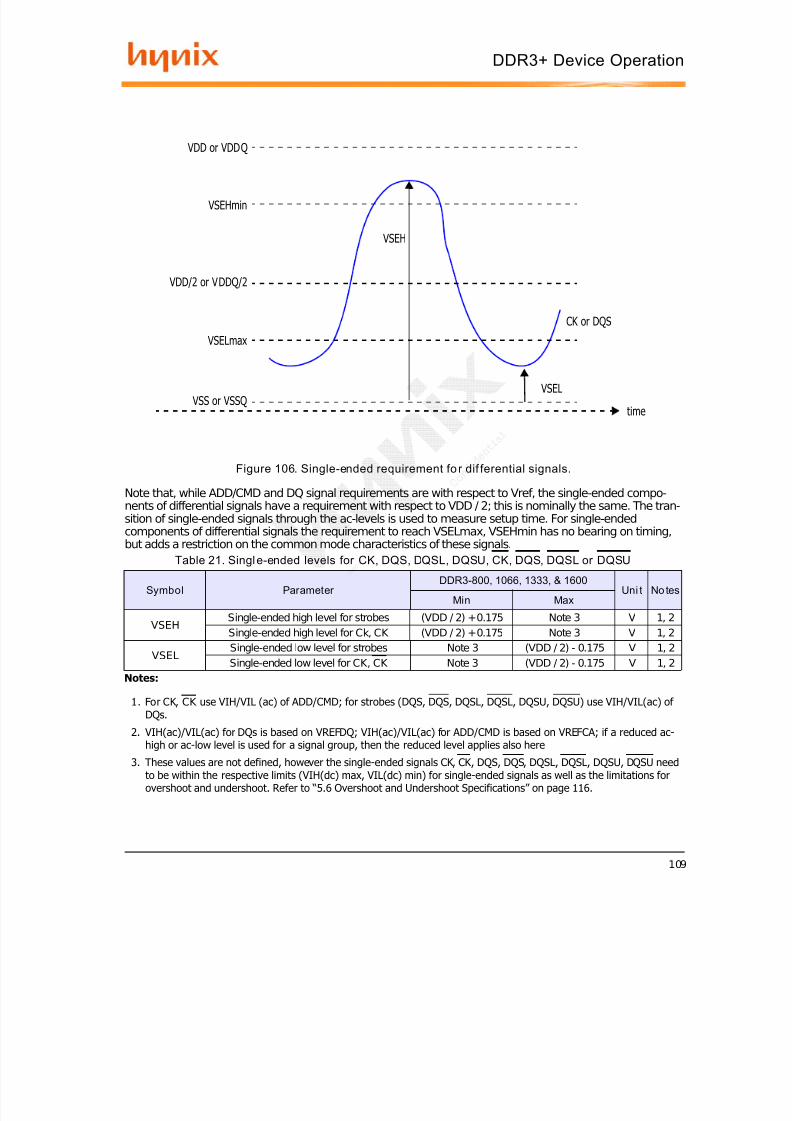
7/29/2019 DDR3 Device Operation Timing Diagram
http://slidepdf.com/reader/full/ddr3-device-operation-timing-diagram 109/154
109
DDR3+ Device Operation
Figure 106. Single-ended requirement fo r dif ferential signals.
Note that, while ADD/CMD and DQ signal requirements are with respect to Vref, the single-ended compo-nents of differential signals have a requirement with respect to VDD / 2; this is nominally the same. The tran-sition of single-ended signals through the ac-levels is used to measure setup time. For single-endedcomponents of differential signals the requirement to reach VSELmax, VSEHmin has no bearing on timing,but adds a restriction on the common mode characteristics of these signals.
VDD or VDDQ
VSEHmin
VDD/2 or VDDQ/2
VSEH
VSELmax
VSS or VSSQ
CK or DQS
VSEL
time
Table 21. Singl e-ended levels for CK, DQS, DQSL, DQSU, CK, DQS, DQSL or DQSU
Symbol Parameter DDR3-800, 1066, 1333, & 1600
Uni t No tesMin Max
VSEHSingle-ended high level for strobes (VDD / 2) +0.175 Note 3 V 1, 2Single-ended high level for Ck, CK (VDD / 2) +0.175 Note 3 V 1, 2
VSELSingle-ended low level for strobes Note 3 (VDD / 2) - 0.175 V 1, 2Single-ended low level for CK, CK Note 3 (VDD / 2) - 0.175 V 1, 2
Notes:
1. For CK, CK use VIH/VIL (ac) of ADD/CMD; for strobes (DQS, DQS, DQSL, DQSL, DQSU, DQSU) use VIH/VIL(ac) of DQs.
2. VIH(ac)/VIL(ac) for DQs is based on VREFDQ; VIH(ac)/VIL(ac) for ADD/CMD is based on VREFCA; if a reduced ac-high or ac-low level is used for a signal group, then the reduced level applies also here
3. These values are not defined, however the single-ended signals CK, CK, DQS, DQS, DQSL, DQSL, DQSU, DQSU needto be within the respective limits (VIH(dc) max, VIL(dc) min) for single-ended signals as well as the limitations forovershoot and undershoot. Refer to “5.6 Overshoot and Undershoot Specifications” on page 116.
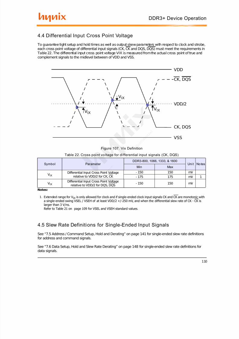
7/29/2019 DDR3 Device Operation Timing Diagram
http://slidepdf.com/reader/full/ddr3-device-operation-timing-diagram 110/154
110
DDR3+ Device Operation
4.4 Differential Input Cross Point Voltage
To guarantee tight setup and hold times as well as output skew parameters with respect to clock and strobe,each cross point voltage of differential input signals (CK, CK and DQS, DQS) must meet the requirements in
Table 22. The differential input cross point voltage VIX is measured from the actual cross point of true andcomplement signals to the midlevel between of VDD and VSS.
Figure 107. Vix Definition
4.5 Slew Rate Definitions for Single-Ended Input Signals See “7.5 Address / Command Setup, Hold and Derating” on page 141 for single-ended slew rate definitionsfor address and command signals. See “7.6 Data Setup, Hold and Slew Rate Derating” on page 148 for single-ended slew rate definitions fordata signals.
VDD
VSS
VDD/2VIX
VIX
VIX
CK, DQS
CK, DQS
Table 22. Cross poi nt vo ltage for di fferential input signals (CK, DQS)
Symbol Parameter DDR3-800, 1066, 1333, & 1600
Uni t No tesMin Max
VIXDifferential Input Cross Point Voltage
relative to VDD/2 for CK, CK - 150 150 mV- 175 175 mV 1
VIXDifferential Input Cross Point Voltage
relative to VDD/2 for DQS, DQS - 150 150 mV
Notes:
1. Extended range for V IX is only allowed for clock and if single-ended clock input signals CK and CK are monotonic witha single-ended swing VSEL / VSEH of at least VDD/2 +/-250 mV, and when the differential slew rate of CK - CK islarger than 3 V/ns.
Refer to Table 21 on page 109 for VSEL and VSEH standard values.
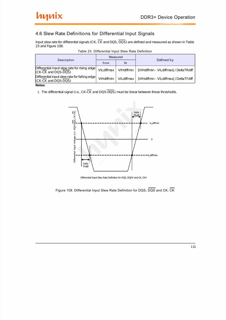
7/29/2019 DDR3 Device Operation Timing Diagram
http://slidepdf.com/reader/full/ddr3-device-operation-timing-diagram 111/154
111
DDR3+ Device Operation
4.6 Slew Rate Definitions for Differential Input Signals Input slew rate for differential signals (CK, CK and DQS, DQS) are defined and measured as shown in Table23 and Figure 108.
Figure 108. Differential Input Slew Rate Definition for DQS, DQS and CK, CK
DeltaTFdiff
DeltaTRdiff
VIHdiffmin
VILdiffmax
0
D i f f e r e n
t i a l I n p
u t V o
l t a g e
( i . e .
D Q S - D
Q S ;
C K - C
K )
Differential Input Slew Rate Definition for DQS, DQS# and CK, CK#
Table 23. Differential Input Slew Rate Definition
DescriptionMeasured
Defined b yfrom to
Differential input slew rate for rising edge(CK-CK and DQS-DQS) VILdiffmax VIHdiffmin [VIHdiffmin - VILdiffmax] / DeltaTRdiff
Differential input slew rate for falling edge(CK-CK and DQS-DQS) VIHdiffmin VILdiffmax [VIHdiffmin - VILdiffmax] / DeltaTFdiff
Notes:
1. The differential signal (i.e., CK-CK and DQS-DQS) must be linear between these thresholds.

7/29/2019 DDR3 Device Operation Timing Diagram
http://slidepdf.com/reader/full/ddr3-device-operation-timing-diagram 112/154
112
DDR3+ Device Operation
5 . AC & DC Out pu t Measure m ent Leve l s
5.1 Single Ended AC and DC Output Levels
Table 24 shows the output levels used for measurements of single ended signals.
5.2 Differential AC and DC Output Levels
Table 25 shows the output levels used for measurements of differential signals.
Table 24. Single-ended AC and DC Outpu t Levels
Symbol ParameterDDR3-800, 1066,
1333 and 1600Unit Notes
VOH(DC) DC output high measurement level (for IV curve linearity) 0.8 x V DDQ V
VOM(DC) DC output mid measurement level (for IV curve linearity) 0.5 x V DDQ V
VOL(DC) DC output low measurement level (for IV curve linearity) 0.2 x V DDQ V
VOH(AC) AC output high measurement level (for output SR) VTT + 0.1 x V DDQ V 1
VOL(AC) AC output low measurement level (for output SR) VTT - 0.1 x V DDQ V 1
Notes:1. The swing of ±0. 1 x V DDQ is based on approximately 50% of the static single-ended output high or low swing with a
driver impedance of 40 Ω and an effective test load of 25 Ω to VTT = V DDQ /2.
Table 25. Differential AC and DC Output Levels
Symbol Parameter
DDR3-800, 1066,
1333 and 1600 Unit Notes
VOHdiff(AC) AC differential output high measurement level (for output SR) + 0.2 x V DDQ V 1
VOLdiff(AC) AC differential output low measurement level (for output SR) - 0.2 x V DDQ V 1Notes:
1. The swing of ±0.2 x VDDQ is based on approximately 50% of the static single-ended output high or low swing with adriver impedance of 40 Ω and an effective test load of 25 Ω to VTT = V DDQ /2 at each of the differential outputs.
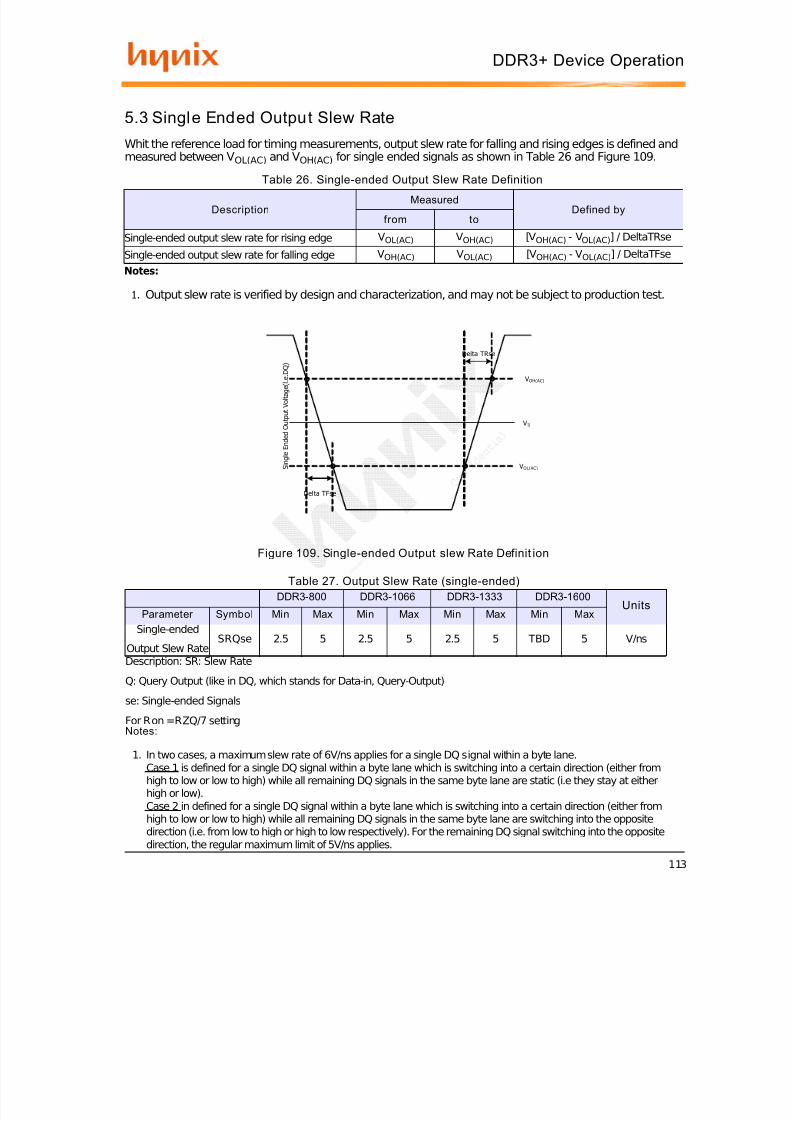
7/29/2019 DDR3 Device Operation Timing Diagram
http://slidepdf.com/reader/full/ddr3-device-operation-timing-diagram 113/154
113
DDR3+ Device Operation
5.3 Single Ended Output Slew Rate
Whit the reference load for timing measurements, output slew rate for falling and rising edges is defined andmeasured between V OL(AC) and V OH(AC) for single ended signals as shown in Table 26 and Figure 109.
Figure 109. Single-ended Output slew Rate Definit ion
Delta TFse
Delta TRse
VOH(AC)
VOL(AC)
V∏
S i n g
l e E n
d e
d O u
t p u
t V o
l t a g e
( l . e . D
Q )
Table 26. Single-ended Output Slew Rate Definition
DescriptionMeasured
Defined byfrom to
Single-ended output slew rate for rising edge VOL(AC) VOH(AC) [VOH(AC) - VOL(AC)] / DeltaTRse
Single-ended output slew rate for falling edge VOH(AC) VOL(AC) [VOH(AC) - VOL(AC)] / DeltaTFseNotes:
1. Output slew rate is verified by design and characterization, and may not be subject to production test.
Table 27. Output Slew Rate (single-ended)DDR3-800 DDR3-1066 DDR3-1333 DDR3-1600
UnitsParameter Symbol Min Max Min Max Min Max Min Max
Single-ended
Output Slew RateSRQse 2.5 5 2.5 5 2.5 5 TBD 5 V/ns
Description: SR: Slew Rate
Q: Query Output (like in DQ, which stands for Data-in, Query-Output)
se: Single-ended Signals
For Ron =RZQ/7 settingNotes:
1. In two cases, a maximum slew rate of 6V/ns applies for a single DQ signal within a byte lane. Case 1 is defined for a single DQ signal within a byte lane which is switching into a certain direction (either fromhigh to low or low to high) while all remaining DQ signals in the same byte lane are static (i.e they stay at eitherhigh or low). Case 2 in defined for a single DQ signal within a byte lane which is switching into a certain direction (either fromhigh to low or low to high) while all remaining DQ signals in the same byte lane are switching into the oppositedirection (i.e. from low to high or high to low respectively). For the remaining DQ signal switching into the oppositedirection, the regular maximum limit of 5V/ns applies.
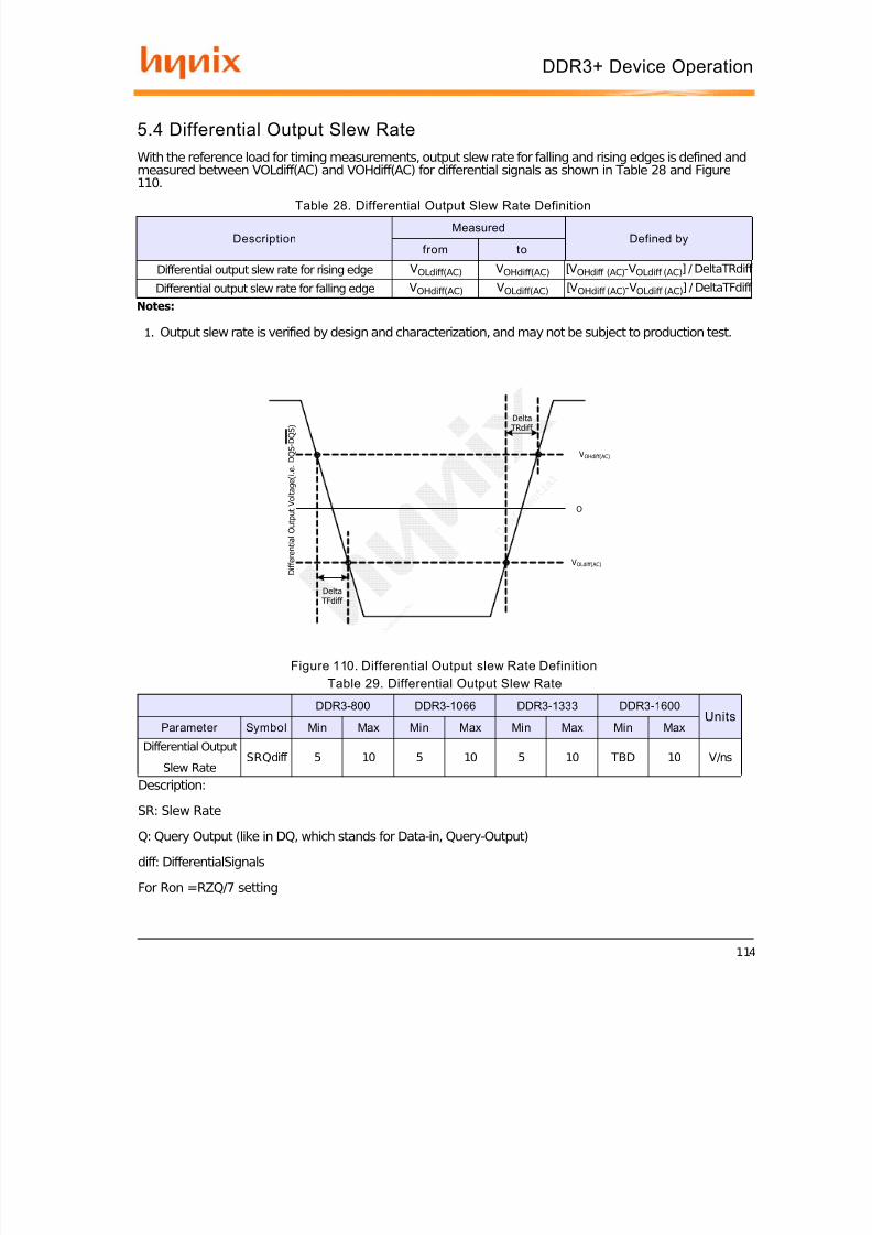
7/29/2019 DDR3 Device Operation Timing Diagram
http://slidepdf.com/reader/full/ddr3-device-operation-timing-diagram 114/154
114
DDR3+ Device Operation
5.4 Differential Output Slew RateWith the reference load for timing measurements, output slew rate for falling and rising edges is defined andmeasured between VOLdiff(AC) and VOHdiff(AC) for differential signals as shown in Table 28 and Figure110.
Figure 110. Differential Output slew Rate Definition
DeltaTFdiff
DeltaTRdiff
VOHdiff(AC)
VOLdiff(AC)
O
D i f f e r e n
t i a l O u
t p u
t V o
l t a g e
( i . e .
D Q S - D
Q S )
Table 28. Differential Output Slew Rate Definition
DescriptionMeasured
Defined byfrom to
Differential output slew rate for rising edge VOLdiff(AC) VOHdiff(AC) [VOHdiff (AC) -VOLdiff (AC) ] / DeltaTRdiff
Differential output slew rate for falling edge VOHdiff(AC) VOLdiff(AC) [VOHdiff (AC) -VOLdiff (AC) ] / DeltaTFdiff Notes:
1. Output slew rate is verified by design and characterization, and may not be subject to production test.
Table 29. Differential Output Slew Rate
DDR3-800 DDR3-1066 DDR3-1333 DDR3-1600Units
Parameter Symbol Min Max Min Max Min Max Min Max
Differential Output
Slew Rate SRQdiff 5 10 5 10 5 10 TBD 10 V/ns
Description:
SR: Slew Rate
Q: Query Output (like in DQ, which stands for Data-in, Query-Output)
diff: DifferentialSignals
For Ron =RZQ/7 setting

7/29/2019 DDR3 Device Operation Timing Diagram
http://slidepdf.com/reader/full/ddr3-device-operation-timing-diagram 115/154
115
DDR3+ Device Operation
5.5 Reference Load for AC Timing and Output Slew Rate
Figure 111. represents the effective reference load of 25 ohms used in defining the relevant AC timing param-eters of the device as well as output slew rate measurements.
It is not intended as a precise representation of any particular system environment or a depiction of the actualload presented by a production tester. System designers should use IBIS or other simulation tools to correlatethe timing reference load to a system environment. Manufacturers correlate to their production test condi-tions, generally one or more coaxial transmission lines terminated at the tester electronics.
Figure 111. Reference Load for AC Timing and Output Slew Rate
DUT
DQDQSDQS
VDDQ
25 Ohm
VTT = VDDQ/2CK, CK
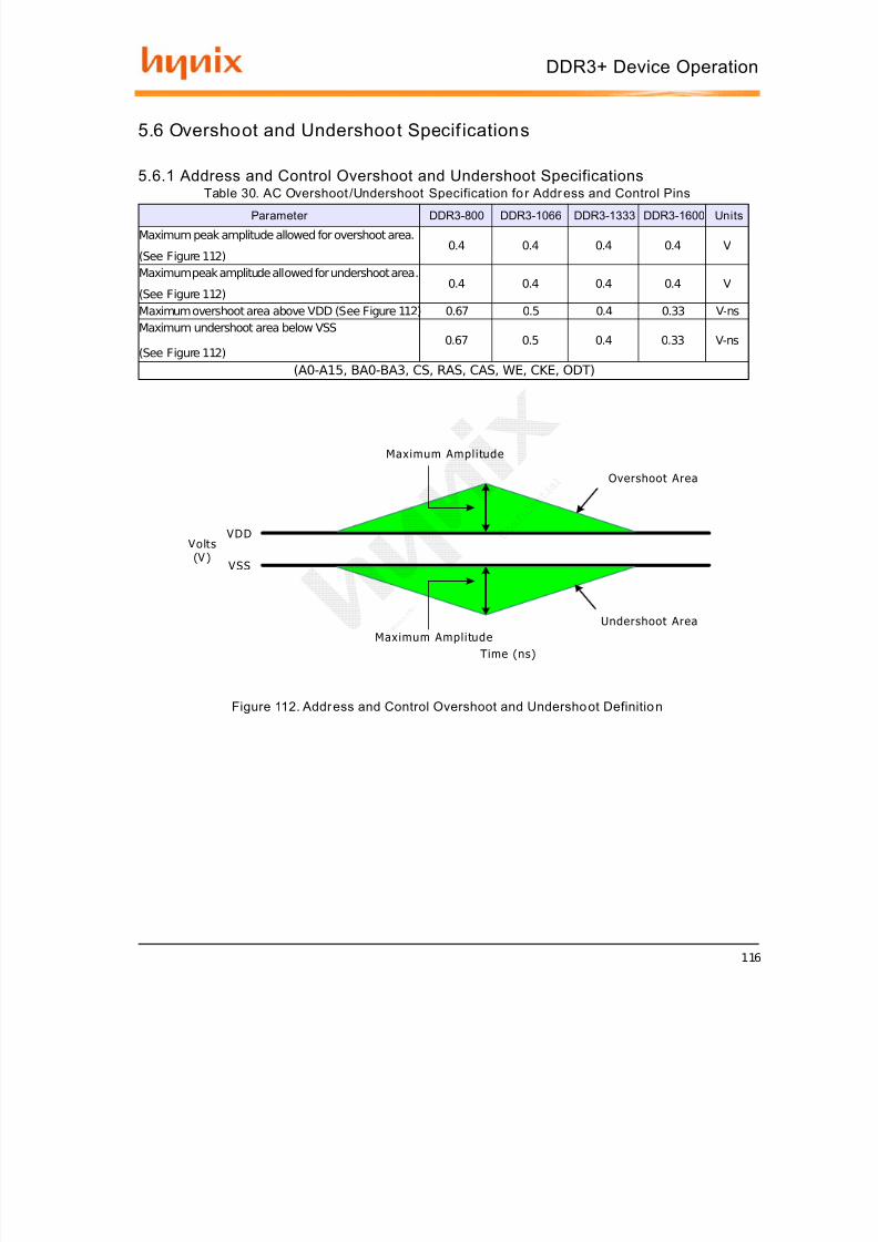
7/29/2019 DDR3 Device Operation Timing Diagram
http://slidepdf.com/reader/full/ddr3-device-operation-timing-diagram 116/154
116
DDR3+ Device Operation
5.6 Overshoot and Undershoot Specif ications
5.6.1 Address and Control Overshoot and Undershoot Specifications
Figure 112. Addr ess and Control Overshoot and Undersho ot Definitio n
Maximum Amplitude
Overshoot Area
VDD
VSS
Maximum AmplitudeUndershoot Area
Time (ns)
Volts(V )
Table 30. AC Overshoot /Undershoot Specification fo r Addr ess and Control PinsParameter DDR3-800 DDR3-1066 DDR3-1333 DDR3-1600 Units
Maximum peak amplitude allowed for overshoot area.
(See Figure 112)0.4 0.4 0.4 0.4 V
Maximum peak amplitude allowed for undershoot area.
(See Figure 112)0.4 0.4 0.4 0.4 V
Maximum overshoot area above VDD (See Figure 112) 0.67 0.5 0.4 0.33 V-nsMaximum undershoot area below VSS
(See Figure 112)0.67 0.5 0.4 0.33 V-ns
(A0-A15, BA0-BA3, CS, RAS, CAS, WE, CKE, ODT)

7/29/2019 DDR3 Device Operation Timing Diagram
http://slidepdf.com/reader/full/ddr3-device-operation-timing-diagram 117/154
117
DDR3+ Device Operation
5.6.2 Clock , Data, Strobe and Mask Overshoot and Undershoot Specifications
Figure 113. Clock, Data, Strobe and Mask Overshoot and Undershoo t Definitio n
Maximum Amplitude
Overshoot Area
VD DQ
VS SQ
Maximum AmplitudeUndershoot Area
Time (ns)
Vo lts(V)
Table 31. AC Overshoo t/Undershoot Specifi cation for Clock, Data, Strobe and Mask
Parameter DDR3-800 DDR3-1066 DDR3-1333 DDR3-1600 Units
Maximum peak amplitude allowed for overshoot area.(See Figure 113)
0.4 0.4 0.4 0.4 V
Maximum peak amplitude allowed for undershoot area.
(See Figure 113)0.4 0.4 0.4 0.4 V
Maximum overshoot area above VDDQ (See Figure 113) 0.25 0.19 0.15 0.13 V-nsMaximum undershoot area below VSSQ
(See Figure 113)0.25 0.19 0.15 0.13 V-ns
(CK, CK, DQ, DQS, DQS, DM)
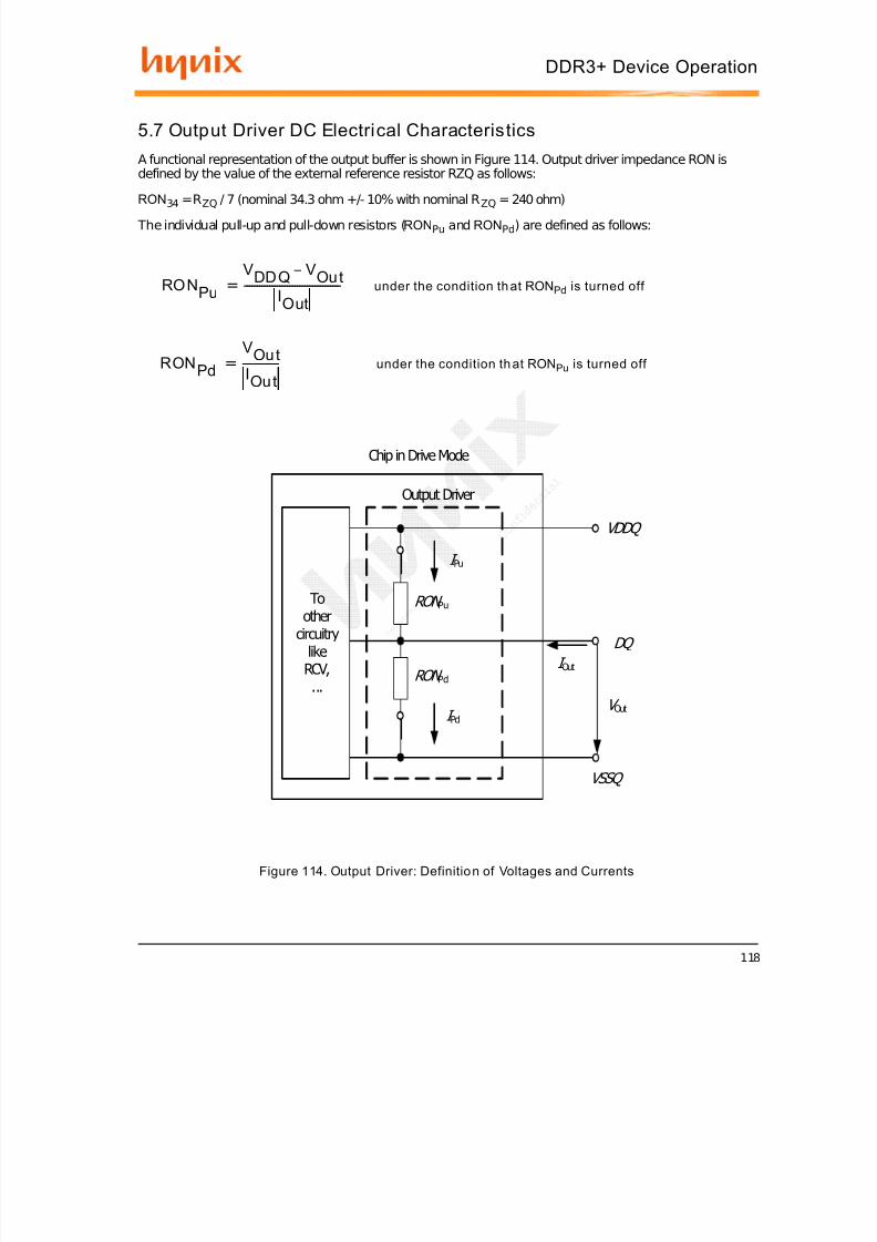
7/29/2019 DDR3 Device Operation Timing Diagram
http://slidepdf.com/reader/full/ddr3-device-operation-timing-diagram 118/154
118
DDR3+ Device Operation
5.7 Output Driver DC Electrical Characteris tics
A functional representation of the output buffer is shown in Figure 114. Output driver impedance RON isdefined by the value of the external reference resistor RZQ as follows:
RON 34 = R ZQ / 7 (nominal 34.3 ohm +/- 10% with nominal R ZQ = 240 ohm)
The individual pull-up and pull-down resistors ( RON Pu and RON Pd ) are defined as follows:
under the condition th at RON Pd is turned off
under the condition th at RON Pu is turned off
Figure 114. Output Driver: Definitio n of Voltages and Currents
RON PuVDDQ VOut–
IOut--------------------------------------=
RON PdVOutIOut
---------------=
Toother
circuitrylike
RCV,...
I Pu
RON Pu
RON Pd
I Pd
Output Driver
I Out
V Out
VSSQ
DQ
VDDQ
Chip in Drive Mode

7/29/2019 DDR3 Device Operation Timing Diagram
http://slidepdf.com/reader/full/ddr3-device-operation-timing-diagram 119/154
119
DDR3+ Device Operation
Table 32. Output Driver DC Electric al Characteristics, assumi ng RZQ = 240 Ω; entire operating temper-ature range; after proper ZQ calibration
RON Nom Resistor VOut min nom max Unit Notes
34 Ω
RON 34Pd
VOLdc =0.2 x VDDQ 0.6 1.0 1.1 RZQ/7 1, 2, 3VOMdc =0.5 x VDDQ 0.9 1.0 1.1 RZQ/7 1, 2, 3VOHdc =0.8 x VDDQ 0.9 1.0 1.4 RZQ/7 1, 2, 3
RON 34Pu
VOLdc =0.2 x VDDQ 0.9 1.0 1.4 RZQ/7 1, 2, 3VOMdc =0.5 x VDDQ 0.9 1.0 1.1 RZQ/7 1, 2, 3VOHdc =0.8 x VDDQ 0.6 1.0 1.1 RZQ/7 1, 2, 3
40 Ω
RON 40Pd
VOLdc =0.2 x VDDQ 0.6 1.0 1.1 RZQ/6 1, 2, 3VOMdc =0.5 x VDDQ 0.9 1.0 1.1 RZQ/6 1, 2, 3VOHdc =0.8 x VDDQ 0.9 1.0 1.4 RZQ/6 1, 2, 3
RON 40PuVOLdc =0.2 x VDDQ 0.9 1.0 1.4 RZQ/6 1, 2, 3VOMdc =0.5 x VDDQ 0.9 1.0 1.1 RZQ/6 1, 2, 3VOHdc =0.8 x VDDQ 0.6 1.0 1.1 RZQ/6 1, 2, 3
Mismatch between pull-up and pull-down,MMPuPd
VOMdc 0.5 x VDDQ
-10 +10 % 1, 2, 4
Notes:
1. The tolerance limits are specified after calibration with stable voltage and temperature. For the behaviorof the tolerance limits if temperature or voltage changes after calibration, see following section on voltageand temperature sensitivity.
2. The tolerance limits are specified under the condition that VDDQ = VDD and that VSSQ = VSS .
3. Pull-down and pull-up output driver impedances are recommended to be calibrated at 0.5 x VDDQ . Othercalibration schemes may be used to achieve the linearity spec shown above, e.g. calibration at 0.2 xVDDQ and 0.8 x VDDQ .
4. Measurement definition for mismatch between pull-up and pull-down, MMPuPd: Measure RON Pu and RON Pd , both at 0.5 * VDDQ :
MMPuPdRON Pu RON Pd–
RON Nom------------------------------------------------- x 100=

7/29/2019 DDR3 Device Operation Timing Diagram
http://slidepdf.com/reader/full/ddr3-device-operation-timing-diagram 120/154
120
DDR3+ Device Operation
5.7.1 Output Driver Temperature and Voltage sensit ivi ty
If temperature and/or voltage change after calibration, the tolerance limits widen according to Table 33 and Table 34.
Δ T = T - T(@calibration); ΔV =VDDQ - VDDQ(@calibration); VDD =VDDQ
Note: dR ONdT and dR ONdV are not subject to production test but are verified by design and characteriza-tion.
Table 33. Output Driver Sensitiv ity Definiti on
min max unit
RONPU@ V OHdc 0.6 - dR ONdTH*| Δ T| - dR ONdVH*| ΔV| 1.1 +dR ONdTH*| Δ T| +dR ONdVH*| ΔV| RZQ/7RON@ V OMdc 0.9 - dR ONdTM*| Δ T| - dR ONdVM*|ΔV| 1.1 +dR ONdTM*| Δ T| +dR ONdVM*| ΔV| RZQ/7
RONPD@ V OLdc 0.6 - dR ONdTL*| Δ T| - dR ONdVL*|ΔV| 1.1 +dR ONdTL*| Δ T| +dR ONdVL*|ΔV| RZQ/7
Table 34. Outpu t Driver Voltage and Temperature Sensitiv ity
Speed Bin800/1066/1333 1600
Unitsmin max min max
dR ONdTM 0 1.5 0 1.5 %/oCdR ONdVM 0 0.15 0 0.13 %/mV
dR ONdTL 0 1.5 0 1.5 %/oCdR ONdVL 0 0.15 0 0.13 %/mV
dRONdTH 0 1.5 0 1.5 %/oCdR
ONdVH 0 0.15 0 0.13 %/mV
These parameters may not be subject to production test. They are verified by design and characterization.

7/29/2019 DDR3 Device Operation Timing Diagram
http://slidepdf.com/reader/full/ddr3-device-operation-timing-diagram 121/154
121
DDR3+ Device Operation
5.8 On-Die Termination (ODT) Levels and I-V Characteris tics
5.8.1 On-Die Termination (ODT) Levels and I-V Characteristics
On-Die Termination effective resistance RTT is defined by bits A9, A6 and A2 of the MR1 Register.
ODT is applied to the DQ, DM, DQS/DQS and TDQS/TDQS (x8 devices only) pins.A functional representation of the on-die termination is shown in Figure 115. The individual pull-up and pull-down resistors ( RTT Pu and RTT Pd ) are defined as follows:
under the condition that RTT Pd is turned off
under the condition that RTT Pu is turned off
Figure 115. On-Die Termination: Definition of Voltages and Currents
RTT Pu
V DDQ V Ou t –I Out
---------------------------------=
RTT Pd
V Ou t
I Ou t -------------=
Toother
circuitrylike
RCV,...
I Pu
RT T Pu
RT T Pd
I Pd
OD T
Iout
V Ou t
VSSQ
DQ
VDDQ
Chip in Termination Mode
I Out = I Pd - I Pu
IO_CTT_DEFINITION_01

7/29/2019 DDR3 Device Operation Timing Diagram
http://slidepdf.com/reader/full/ddr3-device-operation-timing-diagram 122/154
122
DDR3+ Device Operation
5.8.2 ODT DC Electrical Characteristics
Table 35 provides an overview of the ODT DC electrical characteristics. The values for RTT 60Pd120 ,RTT 60Pu120 , RTT 120Pd240 , RTT 120Pu240 , RTT 40Pd80 , RTT 40Pu80 , RTT 30Pd60 , RTT 30Pu60 , RTT 20Pd40 ,
RTT 20Pu40 are not specification requirements, but can be used as design guide lines:Table 35. ODT DC Electri cal Characteri sti cs, assum ing RZQ = 240 Ω+/-1% entire operating temperature
range; after proper ZQ calibration
MR1 A9, A6, A2 RTT Resistor VOut min nom max Unit Notes
0, 1, 0 120 Ω
RTT 120Pd240
VOLdc 0.2 × VDDQ 0.6 1.00 1.1 RZQ 1,2,3,4
0.5 × VDDQ 0.9 1.00 1.1 RZQ 1,2,3,4VOHdc
0.8 × VDDQ 0.9 1.00 1.4 RZQ 1,2,3,4
RTT 120Pu240
VOLdc 0.2 × VDDQ 0.9 1.00 1.4 RZQ 1,2,3,4
0.5 × VDDQ 0.9 1.00 1.1 RZQ 1,2,3,4VOHdc 0.8 × VDDQ 0.6 1.00 1.1 RZQ 1,2,3,4
RTT 120 VIL(ac) to VIH(ac) 0.9 1.00 1.6 RZQ/2 1,2,5
0, 0, 1 60 Ω
RTT 60Pd120
VOLdc 0.2 × VDDQ 0.6 1.00 1.1 RZQ/2 1,2,3,4
0.5 × VDDQ 0.9 1.00 1.1 RZQ/2 1,2,3,4VOHdc
0.8 × VDDQ 0.9 1.00 1.4 RZQ/2 1,2,3,4
RTT 60Pu120
VOLdc 0.2 × VDDQ 0.9 1.00 1.4 RZQ/2 1,2,3,4
0.5 × VDDQ 0.9 1.00 1.1 RZQ/2 1,2,3,4
VOHdc 0.8 × VDDQ 0.6 1.00 1.1 RZQ/2 1,2,3,4
RTT 60 VIL(ac) to VIH(ac) 0.9 1.00 1.6 RZQ/4 1,2,5
0, 1, 1 40 Ω
RTT 40Pd80
VOLdc 0.2 × VDDQ 0.6 1.00 1.1 RZQ/3 1,2,3,4
0.5 × VDDQ 0.9 1.00 1.1 RZQ/3 1,2,3,4VOHdc
0.8 × VDDQ 0.9 1.00 1.4 RZQ/3 1,2,3,4
RTT 40Pu80
VOLdc 0.2 × VDDQ 0.9 1.00 1.4 RZQ/3 1,2,3,4
0.5 × VDDQ 0.9 1.00 1.1 RZQ/3 1,2,3,4VOHdc
0.8 × VDDQ
0.6 1.00 1.1 RZQ/3 1,2,3,4
RTT 40 VIL(ac) to VIH(ac) 0.9 1.00 1.6 RZQ/6 1,2,5

7/29/2019 DDR3 Device Operation Timing Diagram
http://slidepdf.com/reader/full/ddr3-device-operation-timing-diagram 123/154
123
DDR3+ Device Operation
Table 35. ODT DC Electri cal Characteri sti cs, assum ing RZQ = 240 Ω+/-1% entire operating temperaturerange; after proper ZQ calibratio n (Cont’d)
MR1 A9, A6, A2 RTT Resistor VOut min nom max Unit Notes
1, 0, 1 30 Ω
RTT 30Pd60
VOLdc 0.2 × VDDQ 0.6 1.00 1.1 RZQ/4 1,2,3,4
0.5 × VDDQ 0.9 1.00 1.1 RZQ/4 1,2,3,4VOHdc
0.8 × VDDQ 0.9 1.00 1.4 RZQ/4 1,2,3,4
RTT 30Pu60
VOLdc 0.2 × VDDQ 0.9 1.00 1.4 RZQ/4 1,2,3,4
0.5 × VDDQ 0.9 1.00 1.1 RZQ/4 1,2,3,4VOHdc
0.8 × VDDQ 0.6 1.00 1.1 RZQ/4 1,2,3,4
RTT 30 VIL(ac) to VIH(ac) 0.9 1.00 1.6 RZQ/8 1,2,5
1, 0, 0 20 Ω
RTT 20Pd40
VOLdc 0.2 × VDDQ 0.6 1.00 1.1 RZQ/6 1,2,3,40.5 × VDDQ 0.9 1.00 1.1 RZQ/6 1,2,3,4
VOHdc 0.8 × VDDQ 0.9 1.00 1.4 RZQ/6 1,2,3,4
RTT 20Pu40
VOLdc 0.2 × VDDQ 0.9 1.00 1.4 RZQ/6 1,2,3,4
0.5 × VDDQ 0.9 1.00 1.1 RZQ/6 1,2,3,4VOHdc
0.8 × VDDQ 0.6 1.00 1.1 RZQ/6 1,2,3,4
RTT 20 VIL(ac) to VIH(ac) 0.9 1.00 1.6 RZQ/12 1,2,5Deviation of VM w.r.t. VDDQ /2, D VM -5 +5 % 1,2,5,6
Notes:
1. The tolerance limits are specified after calibration with stable voltage and temperature. For the behavior of the toler-ance limits if temperature or voltage changes after calibration, see following section on voltage and temperature sen-sitivity.
2. The tolerance limits are specified under the condition that VDDQ = VDD and that VSSQ = VSS .
3. Pull-down and pull-up ODT resistors are recommended to be calibrated at 0.5 x VDDQ . Other calibration schemesmay be used to achieve the linearity spec shown above, e.g. calibration at 0.2 x VDDQ and 0.8 x VDDQ.
4. Not a specification requirement, but a design guide line.
5. Measurement definition for RTT: Apply VIH(ac) to pin under test and measure current I(VIH(ac) ), then apply VIL(ac) to pin under test and measure currentI(VIL(ac) ) respectively.
Measurement definition for VM and D VM:
Measure voltage ( VM) at test pin (midpoint) with no lo ad:
RTT VIH(ac) VIL(ac)–I(VIH(ac)) I(VIL(ac))–---------------------------------------------------------=
VMΔ 2 VM•
VDDQ------------------ 1–⎝ ⎠⎛ ⎞ 100•=
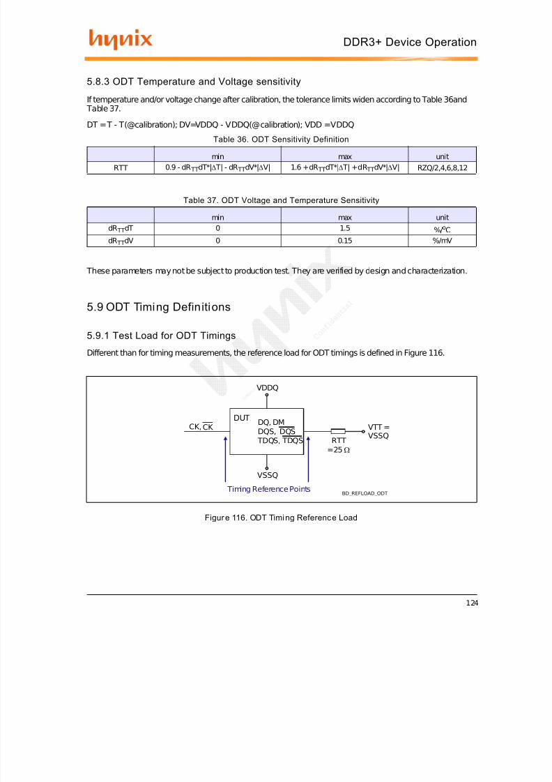
7/29/2019 DDR3 Device Operation Timing Diagram
http://slidepdf.com/reader/full/ddr3-device-operation-timing-diagram 124/154
124
DDR3+ Device Operation
5.8.3 ODT Temperature and Voltage sensitivity
If temperature and/or voltage change after calibration, the tolerance limits widen according to Table 36and Table 37.
DT =T - T(@calibration); DV=VDDQ - VDDQ(@calibration); VDD =VDDQ
These parameters may not be subject to production test. They are verified by design and characterization.
5.9 ODT Timing Definitions
5.9.1 Test Load for ODT Timings
Different than for timing measurements, the reference load for ODT timings is defined in Figure 116.
Figur e 116. ODT Timi ng Reference Load
BD_REFLOAD_ODT
CK CK,
VDDQ
DQSDQS, TDQS TDQS,
DQ, DMDUT
VTT =VSSQ
RTT=25 Ω
VSSQ
Timing Reference Points
Table 36. ODT Sensitivity Definition
min max unit
RTT 0.9 - dR TTdT*| Δ T| - dR TTdV*| ΔV| 1.6 +dR TTdT*| Δ T| +dR TTdV*| ΔV| RZQ/2,4,6,8,12
Table 37. ODT Voltage and Temperature Sensitivity
min max unit
dR TTdT 0 1.5 %/ oC
dR TTdV 0 0.15 %/mV

7/29/2019 DDR3 Device Operation Timing Diagram
http://slidepdf.com/reader/full/ddr3-device-operation-timing-diagram 125/154
125
DDR3+ Device Operation
5.9.2 ODT Timing Definitions
Definitions for tAON, tAONPD, tAOF, tAOFPD and tADC are provided in Table 38 and subsequent figures. Mea-surement reference settings are provided in Table 39.
Table 38. ODT Timing Definitions
Symbol Begin Point Definition End Point Definition Figure
tAON Rising edge of CK - CK defined bythe end point of ODTLon Extrapolated point at VSSQ Figure 117
tAONPD Rising edge of CK - CK withODT being first registered high Extrapolated point at VSSQ Figure 118
tAOF Rising edge of CK - CK defined bythe end point of ODTLoff End point: Extrapolated point at VRTT_Nom Figure 119
tAOFPD Rising edge of CK - CK withODT being first registered low End point: Extrapolated point at VRTT_Nom Figure 120
tADC
Rising edge of CK - CK defined by the end
point of ODTLcnw, ODTLcwn4 or ODTLcwn8
End point: Extrapolated point at VRTT_Wr
and VRTT_Nom respectivelyFigure 121
Table 39. Reference Settings for ODT Timing Measurements
Measured Parameter RTT_Nom Sett ing RTT_Wr Sett ing VSW1 [V] VSW2 [V] Note
tAON R ZQ/4 NA 0.05 0.10
R ZQ/12 NA 0.10 0.20
tAONPD R ZQ/4 NA 0.05 0.10
R ZQ/12 NA 0.10 0.20
tAOF R ZQ/4 NA 0.05 0.10
R ZQ/12 NA 0.10 0.20
tAOFPD R ZQ/4 NA 0.05 0.10
R ZQ/12 NA 0.10 0.20tADC R ZQ/12 R ZQ/2 0.20 0.30
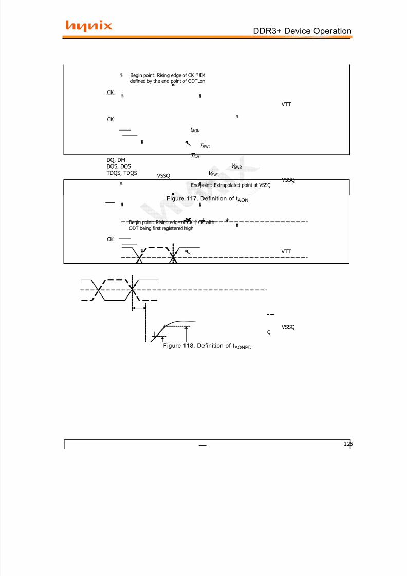
7/29/2019 DDR3 Device Operation Timing Diagram
http://slidepdf.com/reader/full/ddr3-device-operation-timing-diagram 126/154
126
DDR3+ Device Operation
Figure 117. Definition of t AON
Figure 118. Definition of t AONPD
t AON
T SW1
T SW2
V SW1
V SW2
Begin point: Rising edge of CK ? CK defined by the end point of ODTLon
CK
CK
DQ, DMDQS, DQSTDQS, TDQS
VSSQEnd point: Extrapolated point at VSSQ
VSSQ
VTT
t AONPD
T SW1
T SW2
V SW1
V SW2
Begin point: Rising edge of CK ? CK withODT being first registered high
CK
CK
DQ, DMDQS, DQSTDQS, TDQS VSSQ
End point: Extrapolated point at VSSQ VSSQ
VTT
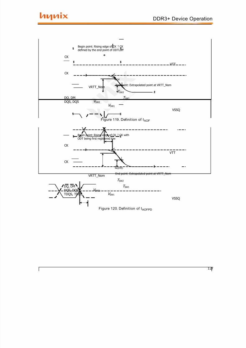
7/29/2019 DDR3 Device Operation Timing Diagram
http://slidepdf.com/reader/full/ddr3-device-operation-timing-diagram 127/154
127
DDR3+ Device Operation
Figure 119. Definit ion of t AOF
Figure 120. Definit ion of t AOFPD
t AOF
V SW2
Begin point: Rising edge of CK ? CK defined by the end point of ODTLoff
CK
CK
DQ, DMDQS, DQSTDQS, TDQS
End point: Extrapolated point at VRTT_Nom
VSSQ
VTT
T SW1
T SW2
V SW1
VRTT_Nom
t AOFPD
V SW2
Begin point: Rising edge of CK ? CK withODT being first registered low
CK
CK
DQ, DMDQS, DQSTDQS, TDQS
End point: Extrapolated point at VRTT_Nom
VSSQ
VTT
T SW1
T SW2
V SW1
VRTT_Nom
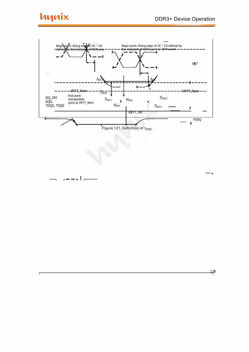
7/29/2019 DDR3 Device Operation Timing Diagram
http://slidepdf.com/reader/full/ddr3-device-operation-timing-diagram 128/154
128
DDR3+ Device Operation
Figure 121. Definit ion of t ADC
t ADC
V SW2
Begin point: Rising edge of CK ? CK defined by the end point of ODTLcnw
CK
CK
DQ, DMDQS, DQSTDQS, TDQS
End point:Extrapolatedpoint at VRTT_Nom
VTT
T SW11
T SW21 VRTT_Nom
t ADC
T SW12
T SW22
V SW1
VRTT_Nom
Begin point: Rising edge of CK ? CK defined bythe end point of ODTLcwn4 or ODTLcwn8
VRTT_Wr
VSSQ
7/29/2019 DDR3 Device Operation Timing Diagram
http://slidepdf.com/reader/full/ddr3-device-operation-timing-diagram 129/154
129
DDR3+ Device Operation
tCK(avg ) = ? tCK j
/ N
j = 1
N
N = 200where
Σ
6 . El ec t r i ca l Cha rac t e r i s t i c s & AC Timing fo r DDR3-800t o DDR3 16 00
6.1 Clock Specification The jitter specified is a random jitter meeting a Gaussian distribution. Input clocks violating the min/max val-ues may result in malfunction of the DDR3 SDRAM device.
6.1.1 Definit ion for tCK(avg)
tCK(avg) is calculated as the average clock period across any consecutive 200 cycle window, where eachclock period is calculated from rising edge to rising edge.
6.1.2 Definit ion for tCK(abs)
tCK(abs) is defined as the absolute clock period, as measured from one rising edge to the next consecutiverising edge. tCK(abs) is not subject to production test.
6.1.3 Definition for tCH(avg) and tCL(avg)tCH(avg) is defined as the average high pulse width, as calculated across any consecutive 200 high pulses.
tCL(avg) is defined as the average low pulse width, as calculated across any consecutive 200 low pulses.
tCH (avg ) = ? tCH j / (N x tCK(avg)) j = 1
N
N = 200where
Σ
tCL(avg ) = ? tCL j / (N x tCK(avg)) j = 1
N
N = 200where
Σ
7/29/2019 DDR3 Device Operation Timing Diagram
http://slidepdf.com/reader/full/ddr3-device-operation-timing-diagram 130/154
130
DDR3+ Device Operation
6.1.4 Definition for tJIT(per) and tJIT(per,lck)
tJ IT(per) = Min/max of tCK i = tCK(avg) where i = 1 to 200.
tJ IT(per) is defined as the largest deviation of any signal tCK from tCK(avg).
tJ IT(per) defines the single period jitter when the DLL is already locked.
tJ IT(per,lck) uses the same definition for single period jitter, during the DLL locking period only.
tJ IT(per) and tJ IT(per,lck) are not subject to production test.
6.1.5 Definit ion for tJIT(cc) and t JIT(cc,lck)
tJ IT(cc) is defined as the absolute difference in clock period between two consecutive clock cycles.
tJ IT(cc) = Max of |tCK i +1 - tCK i|.
tJ IT(cc) defines the cycle to cycle jitter when the DLL is already locked.
tJ IT(cc,lck) uses the same definition for cycle to cycle jitter, during the DLL locking period only.
tJ IT(cc) and tJ IT (cc,lck) are not subject to production test.
6.1.6 Definition for tERR(nper)
tERR is defined as the cumulative error across n multiple consecutive cycles from tCK(avg). tERR is not sub-
ject to production test.
6.2 Refresh parameters by device densityTable 40. Refresh parameters by device density
Notes:
1. Users should refer to the DRAM supplier data sheet and/or the DIMM SPD to determine if DDR3 SDRAM devicessupport the following options or requirements referred to in this material.
Parameter RTT_Nom Setting 1Gb Units NotesREF command to ACT or
REF command time tRFC 110 ns
Average periodic refreshinterval
tREFI0 °C ≤ TCASE ≤ 85 °C 7.8 us
85 °C < TCASE ≤ 95 °C 3.9 us 1
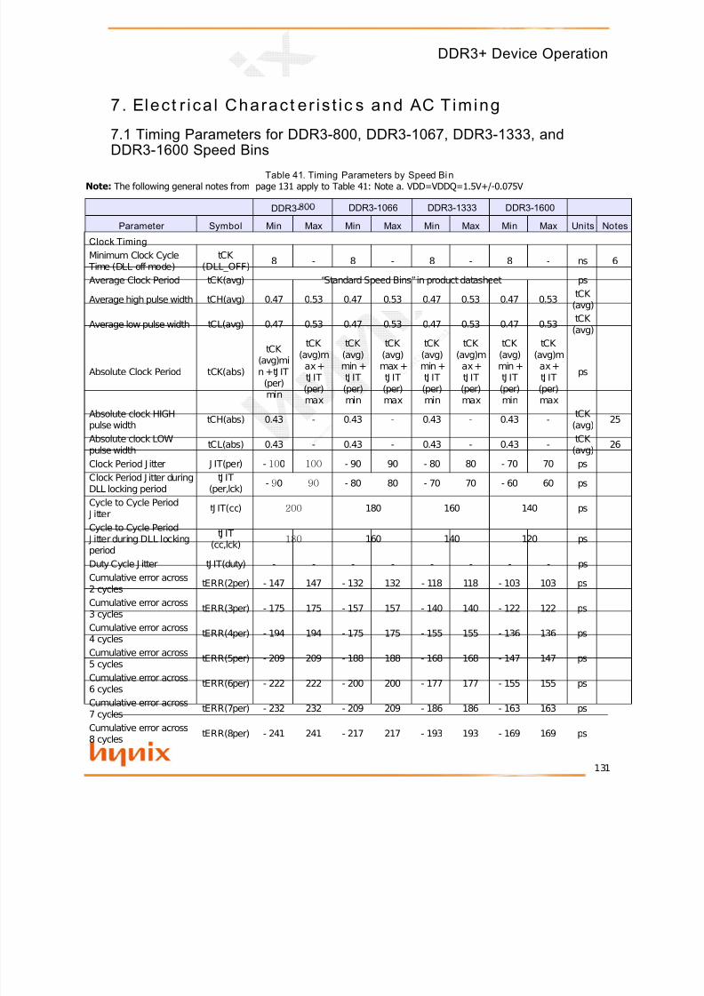
7/29/2019 DDR3 Device Operation Timing Diagram
http://slidepdf.com/reader/full/ddr3-device-operation-timing-diagram 131/154
131
DDR3+ Device Operation
7 . El ec t r i ca l Cha rac t e r i s t i c s and AC Timing
7.1 Timing Parameters for DDR3-800, DDR3-1067, DDR3-1333, and
DDR3-1600 Speed BinsTable 41. Timing Parameters by Speed Bi n
Note: The following general notes from page 131 apply to Table 41: Note a. VDD=VDDQ=1.5V+/-0.075V
DDR3- 800 DDR3-1066 DDR3-1333 DDR3-1600
Parameter Symbol Min Max Min Max Min Max Min Max Units Notes
Clock TimingMinimum Clock Cycle
Time (DLL off mode)tCK
(DLL_OFF) 8 - 8 - 8 - 8 - ns 6
Average Clock Period tCK(avg) “Standard Speed Bins” in product datasheet ps
Average high pulse width tCH(avg) 0.47 0.53 0.47 0.53 0.47 0.53 0.47 0.53 tCK
(avg)Average low pulse width tCL(avg) 0.47 0.53 0.47 0.53 0.47 0.53 0.47 0.53 tCK
(avg)
Absolute Clock Period tCK(abs)
tCK (avg)min +tJ IT
(per)min
tCK (avg)m
ax +tJ IT(per)max
tCK (avg)min +tJ IT(per)min
tCK (avg)max +
tJ IT(per)max
tCK (avg)min +tJ IT(per)min
tCK (avg)m
ax +tJ IT(per)max
tCK (avg)min +tJ IT(per)min
tCK (avg)m
ax +tJ IT(per)max
ps
Absolute clock HIGHpulse width tCH(abs) 0.43 - 0.43 - 0.43 - 0.43 - tCK
(avg) 25
Absolute clock LOWpulse width tCL(abs) 0.43 - 0.43 - 0.43 - 0.43 - tCK
(avg) 26
Clock Period J itter J IT(per) - 10 0 100 - 90 90 - 80 80 - 70 70 psClock Period J itter duringDLL locking period
tJ IT(per,lck) - 9 0 90 - 80 80 - 70 70 - 60 60 ps
Cycle to Cycle Period J itter tJ IT(cc) 200 180 160 140 ps
Cycle to Cycle Period J itter during DLL lockingperiod
tJ IT(cc,lck)
180 160 140 120 ps
Duty Cycle J itter tJ IT(duty) - - - - - - - - psCumulative error across2 cycles tERR(2per) - 147 147 - 132 132 - 118 118 - 103 103 ps
Cumulative error across
3 cyclestERR(3per) - 175 175 - 157 157 - 140 140 - 122 122 ps
Cumulative error across4 cycles tERR(4per) - 194 194 - 175 175 - 155 155 - 136 136 ps
Cumulative error across5 cycles tERR(5per) - 209 209 - 188 188 - 168 168 - 147 147 ps
Cumulative error across6 cycles tERR(6per) - 222 222 - 200 200 - 177 177 - 155 155 ps
Cumulative error across7 cycles tERR(7per) - 232 232 - 209 209 - 186 186 - 163 163 ps
Cumulative error across8 cycles tERR(8per) - 241 241 - 217 217 - 193 193 - 169 169 ps
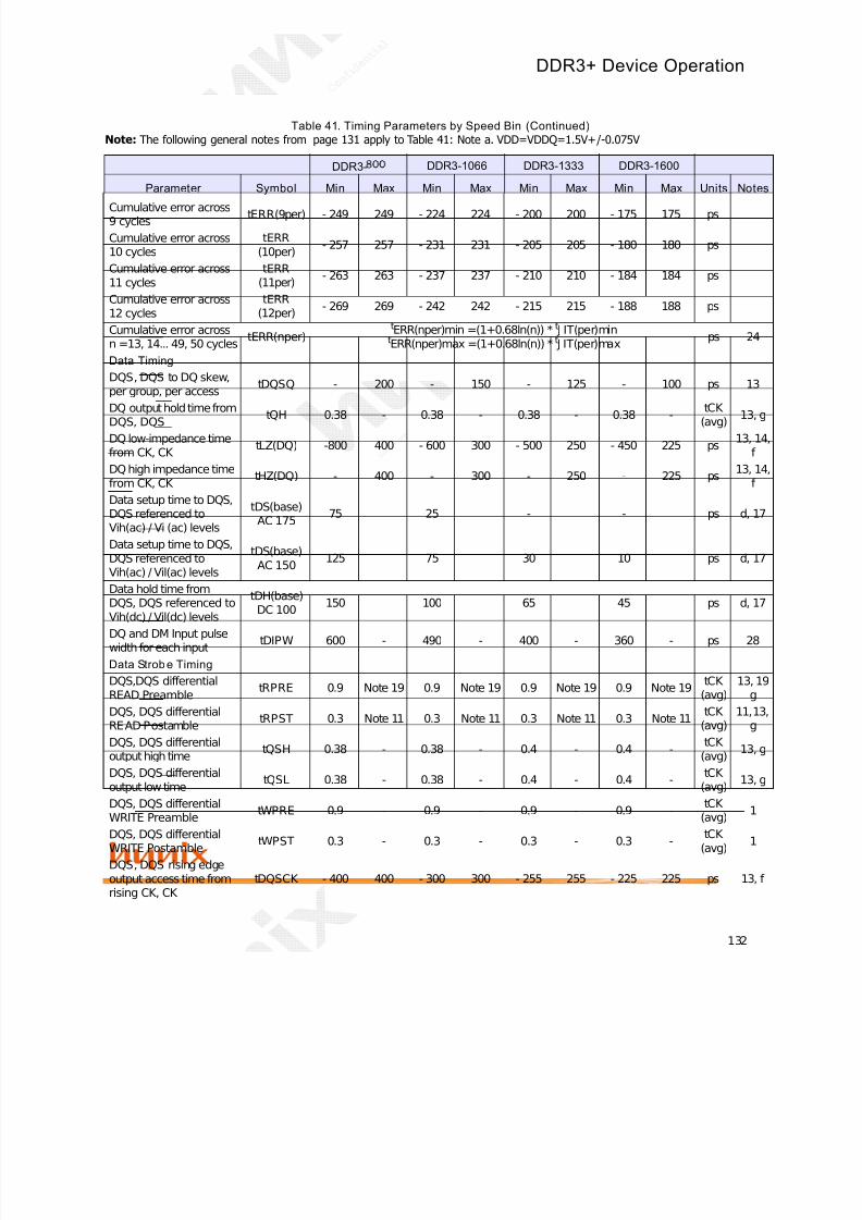
7/29/2019 DDR3 Device Operation Timing Diagram
http://slidepdf.com/reader/full/ddr3-device-operation-timing-diagram 132/154
132
DDR3+ Device Operation
Cumulative error across9 cycles tERR(9per) - 249 249 - 224 224 - 200 200 - 175 175 ps
Cumulative error across10 cycles
tERR(10per) - 257 257 - 231 231 - 205 205 - 180 180 ps
Cumulative error across11 cycles
tERR(11per) - 263 263 - 237 237 - 210 210 - 184 184 ps
Cumulative error across12 cycles
tERR(12per) - 269 269 - 242 242 - 215 215 - 188 188 ps
Cumulative error acrossn =13, 14... 49, 50 cycles tERR(nper)
tERR(nper)min =(1+0.68ln(n)) * t J IT(per)mintERR(nper)max =(1+0.68ln(n)) * t J IT(per)max ps 24
Data Timing
DQS, DQS to DQ skew,per group, per access tDQSQ - 200 - 150 - 125 - 100 ps 13
DQ output hold time fromDQS, DQS tQH 0.38 - 0.38 - 0.38 - 0.38 - tCK
(avg) 13, g
DQ low-impedance timefrom CK, CK tLZ(DQ) -800 400 - 600 300 - 500 250 - 450 225 ps 13, 14,
f DQ high impedance timefrom CK, CK tHZ(DQ) - 400 - 300 - 250 - 225 ps 13, 14,
f Data setup time to DQS,DQS referenced toVih(ac) / Vi (ac) levels
tDS(base)AC 175 75 25 - - ps d, 17
Data setup time to DQS,
DQS referenced toVih(ac) / Vil(ac) levels
tDS(base)AC 150 125 75 30 10 ps d, 17
Data hold time fromDQS, DQS referenced toVih(dc) / Vil(dc) levels
tDH(base)DC 100 150 100 65 45 ps d, 17
DQ and DM Input pulsewidth for each input tDIPW 600 - 490 - 400 - 360 - ps 28
Data Strob e TimingDQS,DQS differentialREAD Preamble tRPRE 0.9 Note 19 0.9 Note 19 0.9 Note 19 0.9 Note 19 tCK
(avg)13, 19
gDQS, DQS differentialREAD Postamble tRPST 0.3 Note 11 0.3 Note 11 0.3 Note 11 0.3 Note 11 tCK
(avg)11, 13,
gDQS, DQS differentialoutput high time tQSH 0.38 - 0.38 - 0.4 - 0.4 -
tCK (avg) 13, g
DQS, DQS differentialoutput low time tQSL 0.38 - 0.38 - 0.4 - 0.4 - tCK
(avg) 13, g
DQS, DQS differentialWRITE Preamble tWPRE 0.9 - 0.9 - 0.9 - 0.9 - tCK
(avg) 1
DQS, DQS differentialWRITE Postamble tWPST 0.3 - 0.3 - 0.3 - 0.3 - tCK
(avg) 1
DQS, DQS rising edgeoutput access time fromrising CK, CK
tDQSCK - 400 400 - 300 300 - 255 255 - 225 225 ps 13, f
Table 41. Timing Parameters by Speed Bin (Continued)Note: The following general notes from page 131 apply to Table 41: Note a. VDD=VDDQ=1.5V+/-0.075V
DDR3- 800 DDR3-1066 DDR3-1333 DDR3-1600
Parameter Symbol Min Max Min Max Min Max Min Max Units Notes

7/29/2019 DDR3 Device Operation Timing Diagram
http://slidepdf.com/reader/full/ddr3-device-operation-timing-diagram 133/154
133
DDR3+ Device Operation
DQS and DQS low-impedance time(Referenced from RL - 1)
tLZ(DQS) - 800 400 - 600 300 - 500 250 - 450 225 ps 13, 14,f
DQS and DQS high-impedance time(Referenced from RL +BL/2)
tHZ(DQS) - 400 - 300 - 250 - 225 ps 13, 14,f
DQS, DQS differentialinput low pulse width tDQSL 0.45 0.55 0.45 0.55 0.45 0.55 0.45 0.55 tCK
(avg) 29, 31
DQS, DQS differentialinput high pulse width tDQSH 0.45 0.55 0.45 0.55 0.45 0.55 0.45 0.55 tCK
(avg) 30, 31
DQS, DQS rising edge toCK, CK rising edge tDQSS - 0.25 0.25 - 0.25 0.25 - 0.25 0.25 - 0.27 0.27 tCK (avg) c
DQS, DQS falling edgesetup time to CK, CK rising edge
tDSS 0.2 - 0.2 - 0.2 - 0.18 - tCK (avg) c, 32
DQS, DQS falling edgehold time from CK, CK rising edge
tDSH 0.2 - 0.2 - 0.2 - 0.18 - tCK (avg) c, 32
Command and Address TimingDLL locking time tDLLK 512 - 512 - 512 - 512 - nCK Internal READ Commandto PRECHARGECommand delay
tRTPmax
(4nCK,7.5ns)
-max
(4nCK,7.5ns)
-max
(4nCK,7.5ns)
-max
(4nCK,7.5ns)
- e
Delay from start of internal write transactionto internal read command
tWTRmax
(4nCK,7.5ns)
-max
(4nCK,7.5ns)
-max
(4nCK,7.5ns)
-max
(4nCK,7.5ns)
- e, 18
WRITE recovery time tWR 15 - 15 - 15 - 15 - ns e, 18Mode Register Setcommand cycle time tMRD 4 - 4 - 4 - 4 - nCK
Mode Register Setcommand update delay tMOD
max(12nCK , 15ns)
-max
(12nCK , 15ns)
-max
(12nCK , 15ns)
-max
(12nCK , 15ns)
-
ACT to internal read orwrite delay time tRCD
Refer to the individual data sheet for its frequencies supported & latencies.
e
PRE command period tRP e
ACT to ACT or REFcommand period tRC e
CAS to CAS commanddelay tCCD 4 - 4 - 4 - 4 - nCK
Auto precharge writerecovery +prechargetime
tDAL(min) WR +roundup(tRP / tCK(avg)) nCK
Multi-Purpose RegisterRecovery Time tMPRR 1 - 1 - 1 - 1 - nCK 22
ACTIVE to PRECHARGEcommand period tRAS Refer to the individual data sheet for its frequencies supported & latencies. e
Table 41. Timing Parameters by Speed Bin (Continued)Note: The following general notes from page 131 apply to Table 41: Note a. VDD=VDDQ=1.5V+/-0.075V
DDR3- 800 DDR3-1066 DDR3-1333 DDR3-1600
Parameter Symbol Min Max Min Max Min Max Min Max Units Notes

7/29/2019 DDR3 Device Operation Timing Diagram
http://slidepdf.com/reader/full/ddr3-device-operation-timing-diagram 134/154
134
DDR3+ Device Operation
ACTIVE to ACTIVEcommand period for 1KBpage size
tRRDmax
(4nCK,10ns)
-max
(4nCK,7.5ns)
-max
(4nCK,6ns)
-max
(4nCK,6ns)
- e
ACTIVE to ACTIVEcommand period for 2KBpage size
tRRDmax
(4nCK,10ns)
-max
(4nCK,10ns)
-max
(4nCK,7.5ns)
-max
(4nCK,7.5ns)
- e
Four activate window for1KB page size tFAW 40 - 37.5 - 30 - 30 - ns e
Four activate window for2KB page size tFAW 50 - 50 - 45 - 40 - ns e
Command and Address
setup time to CK, CK referenced to Vih(ac) /Vil(ac) levels
tIS(base)AC175 200 125 65 45 ps b, 16
Command and Addresssetup time to CK, CK referenced to Vih(ac) /Vil(ac) levels
tIS(base)AC150 350 275 190 170 ps b, 16,
27
Command and Addresshold time from CK, CK referenced to Vih(dc) /Vil(dc) levels
tIH(base)DC100 275 200 140 120 ps b, 16
Control and AddressInput pulse width for each
input
tIPW 900 - 780 - 620 - 560 - ps 28
Calibration Timing
Power-up and RESETcalibration time tZQinit
max(512nC
K,640ns)
-
max(512nC
K,640ns)
-
max(512nC
K,640ns)
-
max(512nC
K,640ns)
-
Normal operation Fullcalibration time tZQoper
max(256nC
K,320ns)
-
max(256nC
K,320ns)
-
max(256nC
K,320ns)
-
max(256nC
K,320ns)
-
Normal operation Shortcalibration time tZQCS
max(64nCK ,80ns)
-max
(64nCK ,80ns)
-max
(64nCK ,80ns)
-max
(64nCK ,80ns)
- 23
Reset Timing
Exit Reset from CKEHIGH to a validcommand
tXPR
max(5nCK,tRFC
(min) +10ns)
-
max(5nCK,tRFC
(min) +10ns)
-
max(5nCK,tRFC
(min) +10ns)
-
max(5nCK,tRFC
(min) +10ns)
-
Self Refresh Timings
Table 41. Timing Parameters by Speed Bin (Continued)Note: The following general notes from page 131 apply to Table 41: Note a. VDD=VDDQ=1.5V+/-0.075V
DDR3- 800 DDR3-1066 DDR3-1333 DDR3-1600
Parameter Symbol Min Max Min Max Min Max Min Max Units Notes

7/29/2019 DDR3 Device Operation Timing Diagram
http://slidepdf.com/reader/full/ddr3-device-operation-timing-diagram 135/154
135
DDR3+ Device Operation
Exit Self Refresh tocommands not requiringa locked DLL
tXS
max(5nCK,tRFC
(min) +10ns)
-
max(5nCK,tRFC
(min) +10ns)
-
max(5nCK,tRFC
(min) +10ns)
-
max(5nCK,tRFC
(min) +10ns)
-
Exit Self Refresh tocommands requiring alocked DLL
tXSDLL tDLLK (min) - tDLLK
(min) - tDLLK (min) - tDLLK
(min) - nCK
Minimum CKE low widthfor Self Refresh entry toexit timing
tCKESRtCKE
(min) +1 nCK
-tCKE
(min) +1 nCK
-tCKE
(min) +1 nCK
-tCKE
(min) +1 nCK
-
Valid Clock Requirementafter Self Refresh Entry(SRE) or Power-DownEntry (PDE)
tCKSREmax
(5 nCK,10 ns)
-max
(5 nCK,10 ns)
-max
(5 nCK,10 ns)
-max
(5 nCK,10 ns)
-
Valid Clock Requirementbefore Self Refresh Exit(SRX) or Power-DownExit (PDX) or Reset Exit
tCKSRXmax
(5 nCK,10 ns)
-max
(5 nCK,10 ns)
-max
(5 nCK,10 ns)
-max
(5 nCK,10 ns)
-
Power Down TimingsExit Power Down withDLL on to any validcommand; ExitPrecharge Power Down
with DLL frozen tocommands not requiringa locked DLL
tXPmax
(3nCK,
7.5ns)
-max
(3nCK,
7.5ns)
-max
(3nCK,
6ns)
-max
(3nCK,
6ns)
-
Exit Precharge PowerDown with DLL frozen tocommands requiring alocked DLL
tXPDLLmax
(10nCK , 24ns)
-max
(10nCK , 24ns)
-max
(10nCK , 24ns)
-max
(10nCK , 24ns)
- 2
CKE minimum pulsewidth tCKE
max(3nCK,7.5ns)
-
max(3nCK,5.625n
s)
-
max(3nCK,5.625n
s)
-max
(3nCK,5ns)
-
Command pass disabledelay tCPDED 1 - 1 - 1 - 1 - nCK
Power Down Entry to Exit Timing tPD tCKE(min) 9 *tREFI tCKE(min) 9 *tREFI tCKE(min) 9 *tREFI tCKE(min) 9 *tREFI 15
Timing of ACT commandto Power Down entry tACTPDEN 1 - 1 - 1 - 1 - nCK 20
Timing of PRE or PREAcommand to PowerDown entry
tPRPDEN 1 - 1 - 1 - 1 - nCK 20
Timing of RD/RDAcommand to PowerDown entry
tRDPDEN RL +4+1 - RL +4
+1 - RL +4+1 - RL +4
+1 - nCK
Table 41. Timing Parameters by Speed Bin (Continued)Note: The following general notes from page 131 apply to Table 41: Note a. VDD=VDDQ=1.5V+/-0.075V
DDR3- 800 DDR3-1066 DDR3-1333 DDR3-1600
Parameter Symbol Min Max Min Max Min Max Min Max Units Notes

7/29/2019 DDR3 Device Operation Timing Diagram
http://slidepdf.com/reader/full/ddr3-device-operation-timing-diagram 136/154
136
DDR3+ Device Operation
Timing of WR commandto Power Down entry(BL8OTF, BL8MRS,BC4OTF)
tWRPDEN
WL+4 +(tWR /
tCK (avg))
-
WL+4 +(tWR /
tCK (avg))
-
WL+4+(tWR /tCK
(avg))
-
WL+4+(tWR /tCK
(avg))
- nCK 9
Timing of WRA commandto Power Down entry(BL8OTF, BL8MRS,BC4OTF)
tWRAPDEN WL+4+WR+1 - WL+4+
WR+1 - WL+4+WR +1 - WL+4+
WR +1 - nCK 10
Timing of WR commandto Power Down entry(BC4MRS)
tWRPDEN
WL+2+(tWR /tCK
(avg))
-
WL+2+(tWR /tCK
(avg))
-
WL+2+(tWR /tCK
(avg))
-
WL+2+(tWR /tCK
(avg))
- nCK 9
Timing of WRA commandto Power Down entry(BC4MRS)
tWRAPDEN WL+2 +WR+1 - WL+2 +
WR+1 - WL+2+WR+1 - WL+2
+WR+1 - nCK 10
Timing of REF commandto Power Down entry tREFPDEN 1 - 1 - 1 - 1 - nCK 20, 21
Timing of MRS commandto Power Down entry tMRSPDEN tMOD
(min) - tMOD(min) - tMOD
(min) - tMOD(min) -
ODT TimingsODT turn on Latency ODTLon WL - 2 =CWL +AL - 2 nCK ODT turn off Latency ODTLoff WL - 2 =CWL +AL - 2 nCK ODT high time withoutwrite command or withwrite command and BC4
ODTH4 4 - 4 - 4 - 4 - nCK
ODT high time with Writecommand and BL8 ODTH8 6 - 6 - 6 - 6 - nCK
Asynchronous RTT turn-on delay (Power-Downwith DLL frozen)
tAONPD 2 8.5 2 8.5 2 8.5 2 8.5 ns
Asynchronous RTT turn-off delay (Power-Downwith DLL frozen)
tAOFPD 2 8.5 2 8.5 2 8.5 2 8.5 ns
RTT turn-on tAON -400 400 -300 300 -250 250 -225 225 ps 7, f RTT_Nom and RTT_WRturn-off time from
ODTLoff reference
tAOF 0.3 0.7 0.3 0.7 0.3 0.7 0.3 0.7 tCK (avg) 8, f
RTT dynamic changeskew tADC 0.3 0.7 0.3 0.7 0.3 0.7 0.3 0.7 tCK
(avg) f
Write Leveling TimingsFirst DQS/DQS risingedge after write levelingmode is programmed
tWLMRD 40 - 40 - 40 - 40 - nCK 3
DQS/DQS delay afterwrite leveling mode isprogrammed
tWLDQSEN 25 - 25 - 25 - 25 - nCK 3
Table 41. Timing Parameters by Speed Bin (Continued)Note: The following general notes from page 131 apply to Table 41: Note a. VDD=VDDQ=1.5V+/-0.075V
DDR3- 800 DDR3-1066 DDR3-1333 DDR3-1600
Parameter Symbol Min Max Min Max Min Max Min Max Units Notes

7/29/2019 DDR3 Device Operation Timing Diagram
http://slidepdf.com/reader/full/ddr3-device-operation-timing-diagram 137/154
137
DDR3+ Device Operation
Write leveling setup timefrom rising CK, CK crossing to rising DQS,DQS crossing
tWLS 325 - 245 - 195 - 165 - ps
Write leveling hold timefrom rising DQS, DQScrossing to rising CK, CK crossing
tWLH 325 - 245 - 195 - 165 - ps
Write leveling outputdelay tWLO 0 9 0 9 0 9 0 7.5 ns
Write leveling outputerror tWLOE 0 2 0 2 0 2 0 2 ns
Table 41. Timing Parameters by Speed Bin (Continued)Note: The following general notes from page 131 apply to Table 41: Note a. VDD=VDDQ=1.5V+/-0.075V
DDR3- 800 DDR3-1066 DDR3-1333 DDR3-1600
Parameter Symbol Min Max Min Max Min Max Min Max Units Notes
7/29/2019 DDR3 Device Operation Timing Diagram
http://slidepdf.com/reader/full/ddr3-device-operation-timing-diagram 138/154
138
DDR3+ Device Operation
7.3 Jitter Notesa. Until ‘tCK (avg)’ represents the actual tCK (avg) of the input clock under operation. Unit ‘nCK’ repre-
sents one clock cycle of the input clock, counting the actual clock edges. ex) tMRD =4[nCK] means;
if one Mode Register Set command is registered at Tm, another Mode Register Set command maybe registered at Tm+4, even if (Tm+4 - Tm) is 4 x tCK (avg) + tERR(4per), min.
b. These parameters are measured from a command/address signal (CKE, CS, RAS, CAS, WE, ODT,BA0, A0, A1, etc.) transition edge to its respective clock signal (CK/CK) crossing. The spec valuesare not affected by the amount of clock jitter applied (i.e. tJ IT (per), tJ IT (cc), etc.), as the setup andhold are relative to the clock signal crossing that latches the command/address. That is, theseparameters should be met whether clock jitter is present or not.
c. These parameters are measured from a data strobe signal (DQS(L/U), DQS(L/U)) crossing to itsrespective clock signal (CK, CK) crossing. The spec values are not affected by the amount of clock
jitter applied (i.e. tJ IT (per), tJ IT (cc), etc.), as these are relative to the clock signal crossing. That is,these parameters should be met whether clock jitter is present or not.
d. These parameters are measured from a data signal (DM(L/U), DQ(L/U)0, DQ(L/U)1, etc.) transitionedge to its respective data strobe signal (DQS(L/U), DQS(L/U)) crossing.
e. For these parameters, the DDR3 SDRAM device supports tnPARAM [nCK] = RU tPARAM [ns] / tCK (avg) [ns], which is in clock cycles, assuming all input clock jitter specifications are satisfied.Forexample, the device will support tnRP =RU tRP / tCK (avg), which is in clock cycles, if all inputclock jitter specifications are met. This means: For DDR3-800 6-6-6, of which tRP =15ns, the devicewill support tnRP =RU tRP / tCK (avg)=6, as long as the input clock jitter specifications are met,i.e. Precharge command at Tm and Active command at Tm+6 is valid even if (Tm+6 - Tm) is lessthan 15ns due to input clock jitter.
f. When the device is operated with input clock jitter, this parameter needs to be derated by the actualtERR (mper), act of the input clock, where 2 <=m <=12.(output deratings are relative to the SDRAMinput clock.)For example, if the measured jitter into a DDR-800 SDRAM has tERR (mper), act, min = -172 ps andtERR (mper), act, max =+ 193 ps, then t DQSCK, min (derated) = tDQSCK, min - tERR (mper), act,max =-400 ps - 193 ps =- 593 ps and tDQSCK, max (derated) =tDQSCK, max - tERR (mper), act,min = 400 ps+ 172 ps = + 572 ps. Similarly, tLZ (DQ) for DDR3-800 derates to tLZ (DQ), min (der-ated) = - 800 ps - 193 ps = - 993 ps and tLZ (DQ), max (derated) = 400 ps + 172 ps = + 572 ps. (Cau-tion on the min/max usage!)Note that tERR (mper), act, min is the minimum measured value of tERR (nper) where 2 <=n <=12,and tERR (mper), act, max is the maximum measured value of tERR (nper) where 2 <= n <= 12
g. When the device is operated with input clock jitter, this parameter needs to be derated by the actualtJ IT (per), act of the input clock. (output deratings are relative to the SDRAM input clock.) For exam-ple, if the measured jitter into a DDR3-800 SDRAM has tCK (avg), act =2500 ps, tJ IT (per), act, min=- 72 ps and tJ IT (per), act, max = +93 ps, then tRPRE, min (derated) = tRPRE, min + tJ IT (per), act,min = 0.9 x tCK (avg), act +tJ IT (per), act + tJ IT (per), act, min = 0.9 x 2500 ps - 72 ps =+ 2178 ps.Similarly, tQH, min (derated) = tQH, min + tJ IT (per), act, min = 0.38 x tCK (avg), act + tJ IT (per), act,min = 0.38 x 2500 ps - 72 ps = + 878 ps. (Caution on the min/max usage!)

7/29/2019 DDR3 Device Operation Timing Diagram
http://slidepdf.com/reader/full/ddr3-device-operation-timing-diagram 139/154
139
DDR3+ Device Operation
7.4 Timing Parameter Notes1. A ctual value dependant upon measurement level definitions See “Figure 41. Method for calculating tWPRE transi-
tions and endpoint” on page 59 and See “Figure 42. Method for calculating tWPST transitions and endpoint” onpage 59 .
2. Commands requiring a locked DLL are: READ (and RAP) and synchronous ODT commands.
3. The max values are system dependent.
4. WR as programmed in mode register.
5. Value must be rounded-up to next higher integer value.
6. There is no maximum cycle time limit besides the need to satisfy the refresh interval, tREFI.
7. For definition of RTT turn-on time tAON See “3.2.2 Timing Parameters” on page 90 .
8. For definition of RTT turn-off time tAOF See “3.2.2 Timing Parameters” on page 90 .
9. tWR is defined in ns, for calculation of tWRPDEN it is necessary to round up tWR / tCK to the next integer.
10. WR in clock cycles as programmed in MR0.
11. The maximum read postamble is bound by tHZDQS(min) plus tQSH(min) on the left side and tHZ(DQS)max on theright side. See “Figure 25. Clock to Data Strobe Relationship” on page 48 .
12. Output timing deratings are relative to the SDRAM input clock. When the device is operated with input clock jitter, thisparameter needs to be derated by t.b.d.
13. Value is only valid for RON34
14. Single ended signal parameter. Refer to chapter <t.b.d.>for definition and measurement method.
15. tREFI depends on TOPER
16. tIS(base) and tIH(base) values are for 1V/ns CMD/ADD single-ended slew rate and 2V/ns CK, CK differential slewrate. Note for DQ and DM signals, VREF(DC) =VRefDQ(DC). For input only pins except RESET, VRef(DC) =VRefCA(DC). See “7.5 Address / Command Setup, Hold and Derating” on page 141 .
17. tDS(base) and tDH(base) values are for 1V/ns DQ single-ended slew rate and 2V/ns DQS, DQS differential slewrate. Note for DQ and DM signals, VREF(DC) =VRefDQ(DC). For input only pins except RESET, VRef(DC) =VRefCA(DC). See “7.6 Data Setup, Hold and Slew Rate Derating” on page 148 .
18. Start of internal write transaction is defined as follows: For BL8 (fixed by MRS and on- the-fly): Rising clock edge 4 clock cycles after WL. For BC4 (on- the- fly): Rising clock edge 4 clock cycles after WL. For BC4 (fixed by MRS): Rising clock edge 2 clock cycles after WL.
19. The maximum read preamble is bound by tLZ(DQS)min on the left side and tDQSCK(max) on the right side. See “Fig-ure 25. Clock to Data Strobe Relationship” on page 48 .
20. CKE is allowed to be registered low while operations such as row activation, precharge, autoprecharge or refresh arein progress, but power-down IDD spec will not be applied until finishing those operations.
21. Although CKE is allowed to be registered LOW after a REFRESH command once tREFPDEN(min) is satisfied, thereare cases where additional time such as tXPDLL(min) is also required. See “2.17.3 Power-Down clarifications - Case2” on page 85 .
22. Defined between end of MPR read burst and MRS which reloads MPR or disables MPR function.
23. One ZQCS command can effectively correct a minimum of 0.5% (ZQ Correction) of RON and RTT impedance errorwithin 64 nCK for all speed bins assuming the maximum sensitivities specified in the ‘Output Driver Voltage and Tem-perature Sensitivity’ and ‘ODT Voltage and Temperature Sensitivity’ tables. The appropriate interval between ZQCScommands can be determined from these tables and other application-specific parameters.
One method for calculating the interval between ZQCS commands, given the temperature (Tdriftrate) and voltage(Vdriftrate) drift rates that the SDRAM is subject to in the application, is illustrated. The interval could be defined bythe following formula:

7/29/2019 DDR3 Device Operation Timing Diagram
http://slidepdf.com/reader/full/ddr3-device-operation-timing-diagram 140/154
140
DDR3+ Device Operation
where TSens =max(dRTTdT, dRONdTM) and VSens =max(dRTTdV, dRONdVM) define the SDRAM temperatureand voltage sensitivities.
For example, if TSens =1.5% / oC, VSens =0.15% / mV, Tdriftrate =1 oC / sec and Vdriftrate =15 mV / sec, then theinterval between ZQCS commands is calculated as:
24. n =from 13 cycles to 50 cycles. This row defines 38 parameters.
25. tCH(abs) is the absolute instantaneous clock high pulse width, as measured from one rising edge to the following fall-ing edge.
26. tCL(abs) is the absolute instantaneous clock low pulse width, as measured from one falling edge to the following ris-ing edge.
27. The tIS(base) AC150 specifications are adjusted from the tIS(base) specification by adding an additional 100 ps of derating to accommodate for the lower alternate threshold of 150 mV and another 25 ps to account for the earlier ref-erence point [(175 mV - 150 mV) / 1 V/ns].
28. Pulse width of a input signal is defined as the width between the first crossing of Vref(dc) and the consecutive cross-ing of Vref(dc).
29. tDQSL describes the instantaneous differential input low pulse width on DQS - DQS, as measured from one falling
edge to the next consecutive rising edge.30. tDQSH describes the instantaneous differential input high pulse width on DQS - DQS, as measured from one rising
edge to the next consecutive falling edge.
31. tDQSH,act +tDQSL,act =1 tCK,act; with tXYZ,act being the actual measured value of the respective timing parame-ter in the application.
32. tDSH,act +tDSS,act =1 tCK,act; with tXYZ,act being the actual measured value of the respective timing parameterin the application.
ZQCorrection(Tsens x Tdriftrate)+( VSens x Vdriftrate)------------------------------------------------------------------------------------------------------------
0.5(1.5 x 1)+(0.15 x 15)------------------------------------------------------ 0.133 128ms≈=
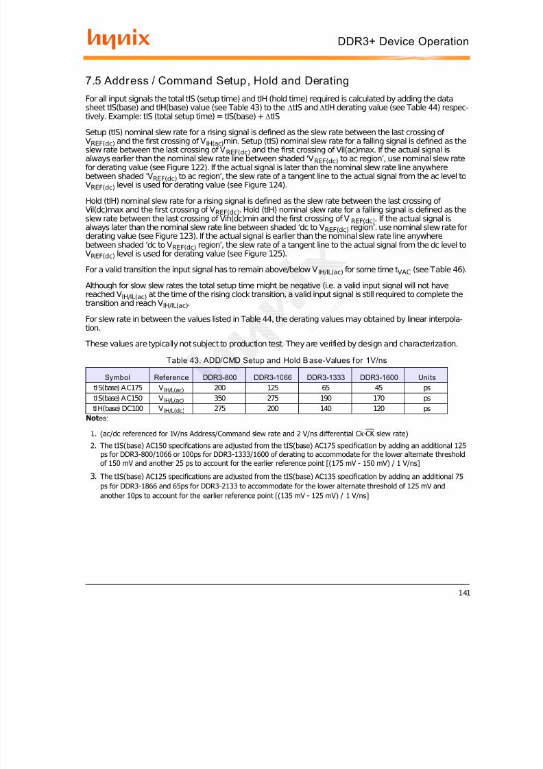
7/29/2019 DDR3 Device Operation Timing Diagram
http://slidepdf.com/reader/full/ddr3-device-operation-timing-diagram 141/154
141
DDR3+ Device Operation
7.5 Address / Command Setup, Hold and Derating
For all input signals the total tIS (setup time) and tIH (hold time) required is calculated by adding the datasheet tIS(base) and tIH(base) value (see Table 43) to the ΔtIS and ΔtIH derating value (see Table 44) respec-
tively. Example: tIS (total setup time) = tIS(base) + ΔtISSetup (tIS) nominal slew rate for a rising signal is defined as the slew rate between the last crossing of VREF(dc) and the first crossing of V IH(ac) min. Setup (tIS) nominal slew rate for a falling signal is defined as theslew rate between the last crossing of V REF(dc) and the first crossing of Vil(ac)max. If the actual signal isalways earlier than the nominal slew rate line between shaded ‘V REF(dc) to ac region’, use nominal slew ratefor derating value (see Figure 122). If the actual signal is later than the nominal slew rate line anywherebetween shaded ‘V REF(dc) to ac region’, the slew rate of a tangent line to the actual signal from the ac level toVREF(dc) level is used for derating value (see Figure 124).
Hold (tIH) nominal slew rate for a rising signal is defined as the slew rate between the last crossing of Vil(dc)max and the first crossing of V REF(dc) . Hold (tIH) nominal slew rate for a falling signal is defined as theslew rate between the last crossing of Vih(dc)min and the first crossing of V REF(dc) . If the actual signal isalways later than the nominal slew rate line between shaded ‘dc to V REF(dc) region’. use nominal slew rate for
derating value (see Figure 123). If the actual signal is earlier than the nominal slew rate line anywherebetween shaded ‘dc to V REF(dc) region’, the slew rate of a tangent line to the actual signal from the dc level toVREF(dc) level is used for derating value (see Figure 125).
For a valid transition the input signal has to remain above/below V IH/IL(ac) for some time t VAC (see Table 46).
Although for slow slew rates the total setup time might be negative (i.e. a valid input signal will not havereached V IH/IL(ac) at the time of the rising clock transition, a valid input signal is still required to complete thetransition and reach V IH/IL(ac) .
For slew rate in between the values listed in Table 44, the derating values may obtained by linear interpola-tion.
These values are typically not subject to production test. They are verified by design and characterization.
Table 43. ADD/CMD Setup and Hold B ase-Values f or 1V/ns
Not es:
1. (ac/dc referenced for 1V/ns Address/Command slew rate and 2 V/ns differential Ck-CK slew rate)
2. The tIS(base) AC150 specifications are adjusted from the tIS(base) AC175 specification by adding an additional 125ps for DDR3-800/1066 or 100ps for DDR3-1333/1600 of derating to accommodate for the lower alternate thresholdof 150 mV and another 25 ps to account for the earlier reference point [(175 mV - 150 mV) / 1 V/ns]
3. The tIS(base) AC125 specifications are adjusted from the tIS(base) AC135 specification by adding an additional 75ps for DDR3-1866 and 65ps for DDR3-2133 to accommodate for the lower alternate threshold of 125 mV andanother 10ps to account for the earlier reference point [(135 mV - 125 mV) / 1 V/ns]
Symbol Reference DDR3-800 DDR3-1066 DDR3-1333 DDR3-1600 UnitstIS(base) AC175 V IH/L(ac) 200 125 65 45 pstIS(base) AC150 V IH/L(ac) 350 275 190 170 pstIH(base) DC100 V IH/L(dc) 275 200 140 120 ps
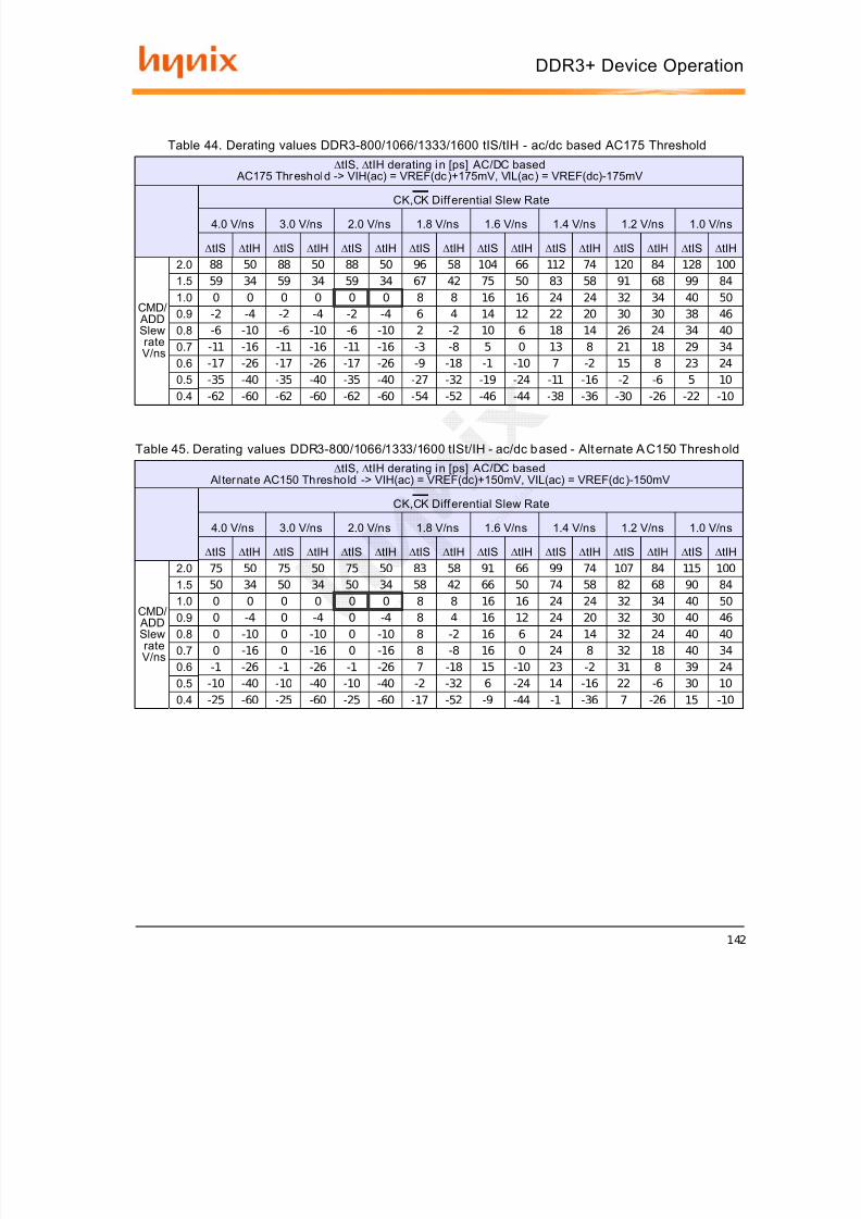
7/29/2019 DDR3 Device Operation Timing Diagram
http://slidepdf.com/reader/full/ddr3-device-operation-timing-diagram 142/154
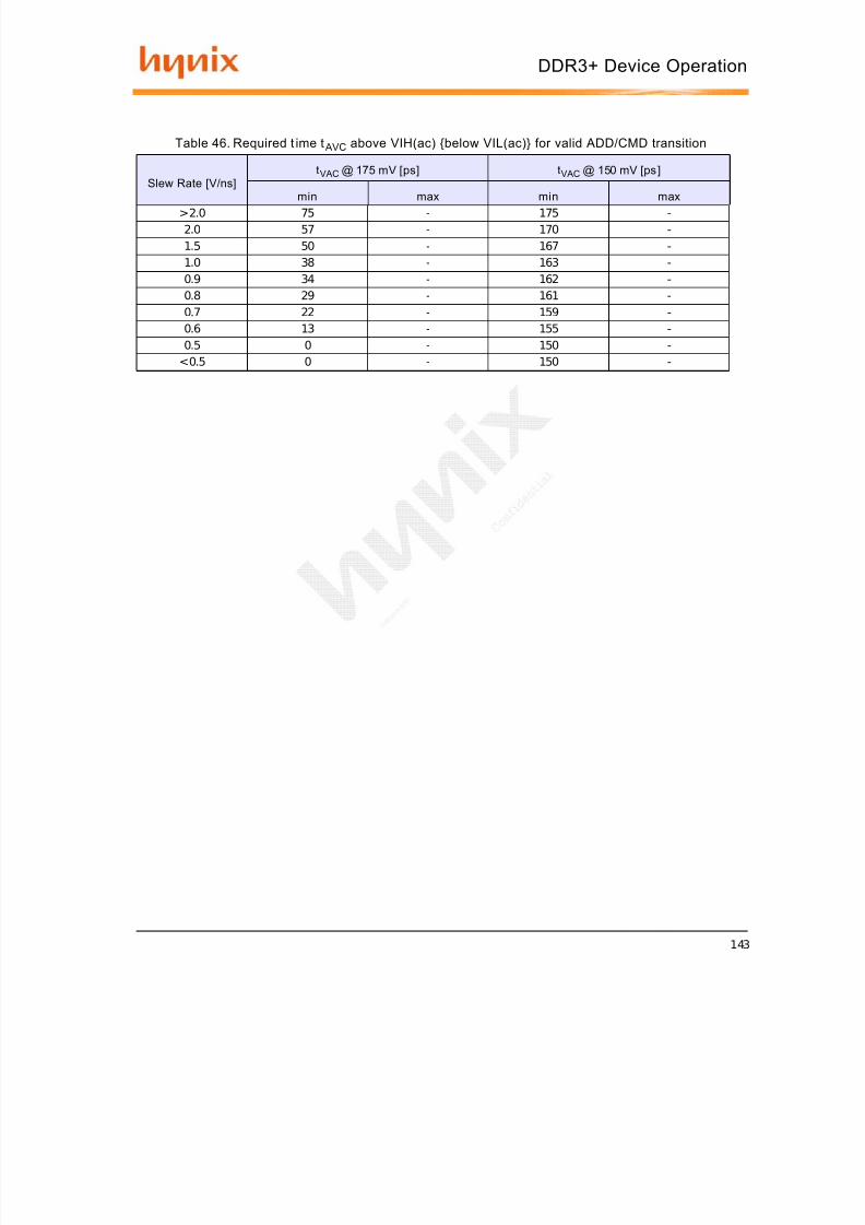
7/29/2019 DDR3 Device Operation Timing Diagram
http://slidepdf.com/reader/full/ddr3-device-operation-timing-diagram 143/154
143
DDR3+ Device Operation
Table 46. Required t ime t AVC above VIH(ac) below VIL(ac) for valid ADD/CMD transition
Slew Rate [V/ns]
tVAC @ 175 mV [ps] t VAC @ 150 mV [ps]
min max min max>2.0 75 - 175 -2.0 57 - 170 -1.5 50 - 167 -1.0 38 - 163 -0.9 34 - 162 -0.8 29 - 161 -0.7 22 - 159 -0.6 13 - 155 -0.5 0 - 150 -
<0.5 0 - 150 -
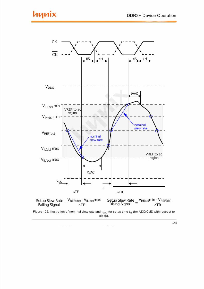
7/29/2019 DDR3 Device Operation Timing Diagram
http://slidepdf.com/reader/full/ddr3-device-operation-timing-diagram 144/154
144
DDR3+ Device Operation
Figure 122. Illustration o f nomi nal slew rate and t VAC for setup time t IS (for A DD/CMD with respect toclock).
VSS
Setup Slew RateSetup Slew RateRising SignalFalling Signal
Δ TF Δ TR
VREF(dc) - VIL(ac) maxΔ TF
=VIH(ac) min - VREF(dc)
Δ TR=
VDDQ
VIH(ac) min
VIH(dc) min
VREF(dc)
VIL(dc) max
VIL(ac) max
nominal
nominalslew rate
VREF to acregion
VREF to acregion
tVAC
tVAC
slew rate
tIHtIStIHtISCK
CK
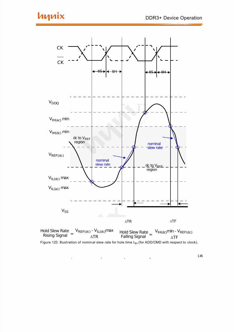
7/29/2019 DDR3 Device Operation Timing Diagram
http://slidepdf.com/reader/full/ddr3-device-operation-timing-diagram 145/154
145
DDR3+ Device Operation
Figure 123. Illust ration of nomin al slew rate for hole time t IH (for ADD/CMD with respect to clock).
VSS
Hold Slew RateHold Slew RateFalling SignalRising Signal
Δ TR Δ TF
VREF(dc) - VIL(dc) maxΔ TR
=VIH(dc) min - VREF(dc)
Δ TF=
VDDQ
VIH(ac) min
VIH(dc) min
VREF(dc)
VIL(dc) max
VIL(ac) max
nominalslew rate
nominalslew rate
dc to V REFregion
dc to V REFregion
CK
CK
tIS tIH tIS tIH
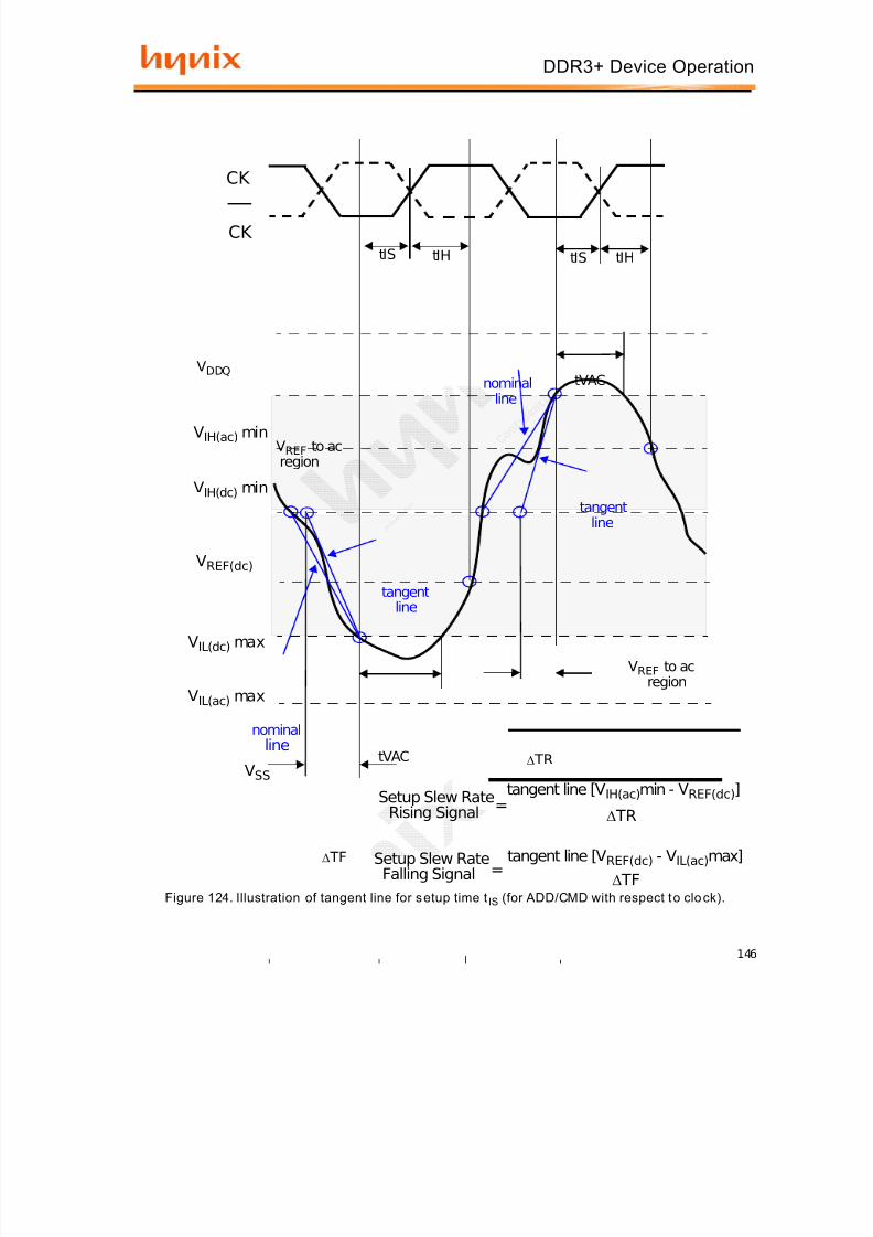
7/29/2019 DDR3 Device Operation Timing Diagram
http://slidepdf.com/reader/full/ddr3-device-operation-timing-diagram 146/154
146
DDR3+ Device Operation
Figure 124. Illustration of tangent line for s etup time t IS (for ADD/CMD with respect t o clo ck).
VSS
Setup Slew Rate
Setup Slew Rate
Rising Signal
Falling SignalΔ TF
Δ TR
tangent line [ VREF(dc) - VIL(ac) max]Δ TF
=
tangent line [V IH(ac) min - VREF(dc) ]Δ TR
=
VDDQ
VIH(ac) min
VIH(dc) min
VREF(dc)
VIL(dc) max
VIL(ac) max
tangent
tangent
VREF to acregion
VREF to acregion
line
line
nominalline
nominalline
tVAC
tVAC
CK
CK
tIS tIH tIS tIH

7/29/2019 DDR3 Device Operation Timing Diagram
http://slidepdf.com/reader/full/ddr3-device-operation-timing-diagram 147/154
147
DDR3+ Device Operation
Figure 125. Illustration of tangent line for s etup time t IH (for ADD/CMD with respect t o cl ock).
VSS
Hold Slew Rate
Δ TFΔ TR
tangent line [V IH(dc) min - VREF(dc) ]Δ TF
=
VDDQ
VIH(ac) min
VIH(dc) min
VREF(dc)
VIL(dc) max
VIL(ac) max
tangent
tangentdc to V REFregion
dc to V REFregion
line
linenominal
line
nominalline
Falling Signal
Hold Slew Rate tangent line [ VREF(dc) - VIL(dc) max]Δ TR= Rising Signal
CK
tIS tIH tIS tIH
CK

7/29/2019 DDR3 Device Operation Timing Diagram
http://slidepdf.com/reader/full/ddr3-device-operation-timing-diagram 148/154
148
DDR3+ Device Operation
7.6 Data Setup, Hold and Slew Rate Derating
For all input signals the total tDS (setup time) and tDH (hold time) required is calculated by adding the datasheet tDS(base) and tDH(base) value (see Table 47) to the ΔtDS and ΔtDH (see Table 48) derating value
respectively. Example: tDS (total setup time) = tDS(base) + ΔtDS.Setup (tDS) nominal slew rate for a rising signal is defined as the slew rate between the last crossing of VREF(dc) and the first crossing of V IH(ac) min. Setup (tDS) nominal slew rate for a falling signal is defined as theslew rate between the last crossing of V REF(dc) and the first crossing of V IL(ac) max (see Figure 126). If theactual signal is always earlier than the nominal slew rate line between shaded ‘V REF(dc) to ac region’, usenominal slew rate for derating value. If the actual signal is later than the nominal slew rate line anywherebetween shaded ‘V REF(dc) to ac region’, the slew rate of a tangent line to the actual signal from the ac level toVREF(dc) level is used for derating value (see Figure 128).
Hold (tDH) nominal slew rate for a rising signal is defined as the slew rate between the last crossing of VIL(dc) max and the first crossing of V REF(dc) . Hold (tDH) nominal slew rate for a falling signal is defined as theslew rate between the last crossing of V IH(dc) min and the first crossing of V REF(dc) (see Figure 127). If theactual signal is always later than the nominal slew rate line between shaded ‘dc level to V REF(dc) region’, use
nominal slew rate for derating value. If the actual signal is earlier than the nominal slew rate line anywherebetween shaded ‘dc to V REF(dc) region’, the slew rate of a tangent line to the actual signal from the dc level toVREF(dc) level is used for derating value (see Figure 129).
For a valid transition the input signal has to remain above/below V IH/IL(ac) for some time t VAC (see Table 50).
Although for slow slew rates the total setup time might be negative (i.e. a valid input signal will not havereached V IH/IL(ac) at the time of the rising clock transition) a valid input signal is still required to complete thetransition and reach V IH/IL(ac) .
For slew rates in between the values listed in the tables the derating values may obtained by linear interpola-tion.
These values are typically not subject to production test. They are verified by design and characterization.
Table 47. Data Setup and Hold B ase-Values
Not es:
1. (ac/dc referenced for 1V/ns DQ-slew rate and 2 V/ns DQS slew rate)
Symbol Reference DDR3-800 DDR3-1066 DDR3-1333 DDR3-1600 UnitstDS(base) AC175 V IH/L(ac) 75 25 - - pstDS(base) AC150 V IH/L(ac) 125 75 30 10 pstDH(base) DC100 V IH/L(dc) 150 100 65 45 ps
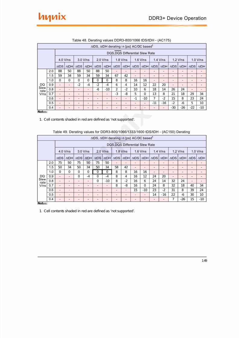
7/29/2019 DDR3 Device Operation Timing Diagram
http://slidepdf.com/reader/full/ddr3-device-operation-timing-diagram 149/154
149
DDR3+ Device Operation
Table 48. Derating values DDR3-800/1066 tDS/tDH - (AC175)
Not es:
1. Cell contents shaded in red are defined as ‘not supported’.
ΔtDS, ΔtDH derating i n [ps] AC/DC based 1
DQS,DQS Differential Slew Rate
4.0 V/ns 3.0 V/ns 2.0 V/ns 1.8 V/ns 1.6 V/ns 1.4 V/ns 1.2 V/ns 1.0 V/ns
ΔtDS ΔtDH ΔtDS ΔtDH ΔtDS ΔtDH ΔtDS ΔtDH ΔtDS ΔtDH ΔtDS ΔtDH ΔtDS ΔtDH ΔtDS ΔtDH
DQSlewrateV/ns
2.0 88 50 88 50 88 50 - - - - - - - - - -1.5 59 34 59 34 59 34 67 42 - - - - - - - -1.0 0 0 0 0 0 0 8 8 16 16 - - - - - -0.9 - - -2 -4 -2 -4 6 4 14 12 22 20 - - - -0.8 - - - - -6 -10 2 -2 10 6 18 14 26 24 - -0.7 - - - - - - -3 -8 5 0 13 8 21 18 29 340.6 - - - - - - - - -1 -10 7 -2 15 8 23 24
0.5 - - - - - - - - - - -11 -16 -2 -6 5 100.4 - - - - - - - - - - - - -30 -26 -22 -10
Table 49. Derating values for DDR3-800/1066/1333/1600 tDS/tDH - (AC150) Derating
Not es:
1. Cell contents shaded in red are defined as ‘not supported’.
ΔtDS, ΔtDH derating i n [ps] AC/DC based 1
DQS,DQS Differential Slew Rate
4.0 V/ns 3.0 V/ns 2.0 V/ns 1.8 V/ns 1.6 V/ns 1.4 V/ns 1.2 V/ns 1.0 V/ns
ΔtDS ΔtDH ΔtDS ΔtDH ΔtDS ΔtDH ΔtDS ΔtDH ΔtDS ΔtDH ΔtDS ΔtDH ΔtDS ΔtDH ΔtDS ΔtDH
DQSlewrateV/ns
2.0 75 50 75 50 75 50 - - - - - - - - - -1.5 50 34 50 34 50 34 58 42 - - - - - - - -1.0 0 0 0 0 0 0 8 8 16 16 - - - - - -0.9 - - 0 -4 0 -4 8 4 16 12 24 20 - - - -0.8 - - - - 0 -10 8 -2 16 6 24 14 32 24 - -0.7 - - - - - - 8 -8 16 0 24 8 32 18 40 340.6 - - - - - - - - 15 -10 23 -2 31 8 39 240.5 - - - - - - - - - - 14 -16 22 -6 30 100.4 - - - - - - - - - - - - 7 -26 15 -10
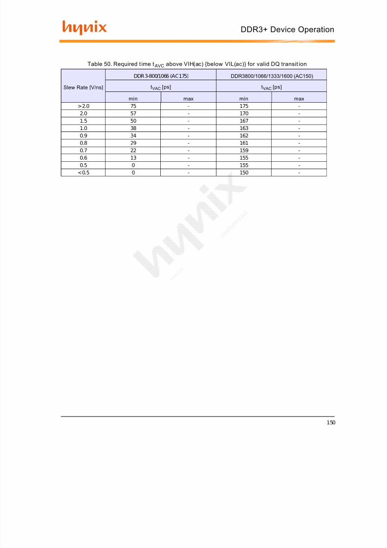
7/29/2019 DDR3 Device Operation Timing Diagram
http://slidepdf.com/reader/full/ddr3-device-operation-timing-diagram 150/154
150
DDR3+ Device Operation
Table 50. Required t ime t AVC above VIH(ac) below VIL(ac) for valid DQ transit ion
Slew Rate [V/ns]
DDR3-800/1066 (AC175) DDR3800/1066/1333/1600 (AC150)
tVAC [ps] t VAC [ps]
min max min max>2.0 75 - 175 -2.0 57 - 170 -1.5 50 - 167 -1.0 38 - 163 -0.9 34 - 162 -0.8 29 - 161 -0.7 22 - 159 -0.6 13 - 155 -0.5 0 - 155 -
<0.5 0 - 150 -
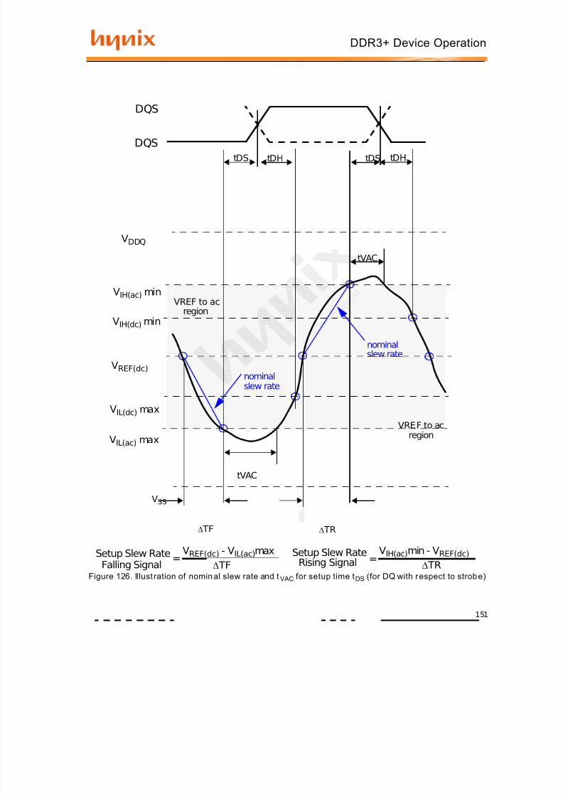
7/29/2019 DDR3 Device Operation Timing Diagram
http://slidepdf.com/reader/full/ddr3-device-operation-timing-diagram 151/154
151
DDR3+ Device Operation
Figure 126. Illust ration of nomin al slew rate and t VAC for setup time t DS (for DQ with r espect to strob e)
VSS
Setup Slew RateSetup Slew RateRising SignalFalling Signal
Δ TF Δ TR
VREF(dc) - VIL(ac) maxΔ TF
=VIH(ac) min - VREF(dc)
Δ TR=
VDDQ
VIH(ac) min
VIH(dc) min
VREF(dc)
VIL(dc) max
VIL(ac) max
nominal
nominalslew rate
VREF to acregion
VREF to acregion
tVAC
tVAC
slew rate
tDHtDS
DQS
DQS
tDHtDS
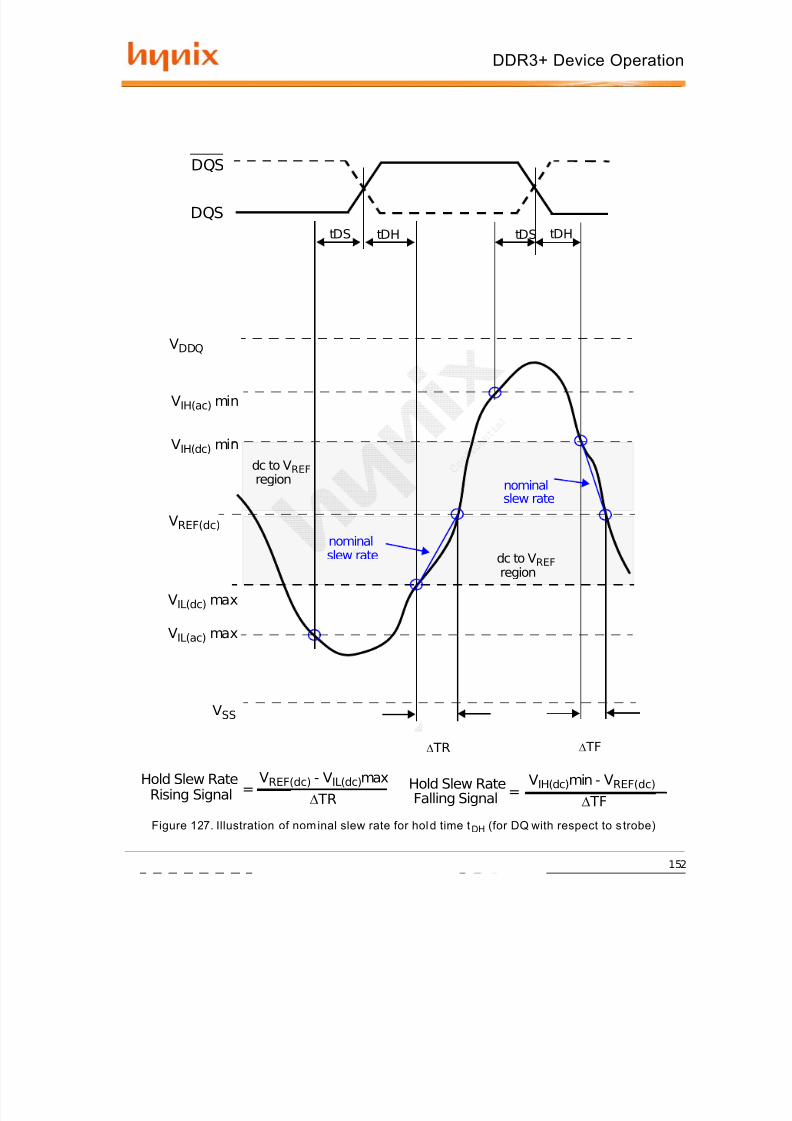
7/29/2019 DDR3 Device Operation Timing Diagram
http://slidepdf.com/reader/full/ddr3-device-operation-timing-diagram 152/154
152
DDR3+ Device Operation
Figure 127. Illustration of nom inal slew rate for hol d time t DH (for DQ with respect to s trobe)
VSS
Hold Slew RateHold Slew RateFalling SignalRising Signal
Δ TR Δ TF
VREF(dc) - VIL(dc) maxΔ TR
=VIH(dc) min - VREF(dc)
Δ TF=
VDDQ
VIH(ac) min
VIH(dc) min
VREF(dc)
VIL(dc) max
VIL(ac) max
nominalslew rate
nominalslew rate
dc to V REFregion
dc to V REFregion
tDHtDS
DQS
DQS
tDHtDS
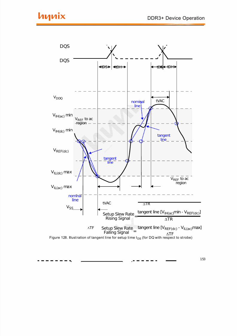
7/29/2019 DDR3 Device Operation Timing Diagram
http://slidepdf.com/reader/full/ddr3-device-operation-timing-diagram 153/154
153
DDR3+ Device Operation
Figure 128. Illust ration of tangent li ne for setup ti me t DS (for DQ with respect to st robe)
VSS
tDH
Setup Slew Rate
Setup Slew Rate
Rising Signal
Falling SignalΔ TF
Δ TR
tangent line [ VREF(dc) - VIL(ac) max]Δ TF
=
tangent line [V IH(ac) min - VREF(dc) ]Δ TR
=
VDDQ
VIH(ac) min
VIH(dc) min
VREF(dc)
VIL(dc) max
VIL(ac) max
tDS
tangent
tangent
VREF to acregion
VREF to acregion
line
line
nominalline
nominalline
tVAC
tVAC
DQS
DQS
tDHtDS
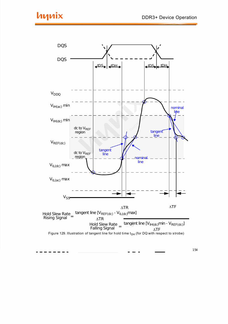
7/29/2019 DDR3 Device Operation Timing Diagram
http://slidepdf.com/reader/full/ddr3-device-operation-timing-diagram 154/154
DDR3+ Device Operation
VDDQ
VIH(ac) min
VIH(dc) min
tangentdc to V REFregion
line
nominalline
tDHtDS
DQS
DQS
tDHtDS