Embed Size (px)
Citation preview

HAL Id: hal-01718637https://hal.archives-ouvertes.fr/hal-01718637
Submitted on 27 Feb 2018
HAL is a multi-disciplinary open accessarchive for the deposit and dissemination of sci-entific research documents, whether they are pub-lished or not. The documents may come fromteaching and research institutions in France orabroad, or from public or private research centers.
L’archive ouverte pluridisciplinaire HAL, estdestinée au dépôt et à la diffusion de documentsscientifiques de niveau recherche, publiés ou non,émanant des établissements d’enseignement et derecherche français ou étrangers, des laboratoirespublics ou privés.
Experimental investigation of the vibrational density ofstates and electronic excitations in metallic nanocrystals
Maxime Bayle, Patrizio Benzo, Nicolas Combe, Christophe Gatel, CarolineBonafos, Gérard Benassayag, Robert Carles
To cite this version:Maxime Bayle, Patrizio Benzo, Nicolas Combe, Christophe Gatel, Caroline Bonafos, et al.. Experimen-tal investigation of the vibrational density of states and electronic excitations in metallic nanocrystals.Physical Review B: Condensed Matter and Materials Physics (1998-2015), American Physical Society,2014, 89 (19), pp.195402. �10.1103/PhysRevB.89.195402�. �hal-01718637�

PHYSICAL REVIEW B 89, 195402 (2014)
Experimental investigation of the vibrational density of states and electronic excitationsin metallic nanocrystals
M. Bayle, P. Benzo, N. Combe, C. Gatel, C. Bonafos, G. Benassayag, and R. Carles*
CEMES-CNRS Universite de Toulouse 29 rue Jeanne Marvig, BP 94347, 31055 Toulouse Cedex 4, France(Received 10 January 2014; revised manuscript received 16 April 2014; published 5 May 2014)
An investigation of the vibrational density of states (VDOS) in silver nanocrystals is performed using Ramanscattering. A specific sample architecture, setup configuration, and original elaboration process are used inorder to take simultaneously advantage of spectrally and spatially localized surface plasmon resonance, opticalamplification, and dark-field spectroscopy. Disentangling the contributions of atom vibrations and electron-holeexcitations (i.e., the so-called “background” in surface-enhanced Raman scattering) is performed. The extractedVDOS is successfully compared with theoretical ones obtained by atomic scale simulations. The effects of size,strain, and disorder on the VDOS are analyzed; in particular, the strain effect is investigated experimentally usingthe geometrical phase analysis coupled with high-resolution transmission electron microscopy. This work offersan opportunity to examine thermodynamic properties, like specific heat, at the nanoscale.
DOI: 10.1103/PhysRevB.89.195402 PACS number(s): 63.22.Kn, 78.30.Er, 73.22.Lp, 65.80.−g
I. INTRODUCTION
Studies on metallic nanocrystals (NCs) are the subject ofnumerous works, either experimental or theoretical, due totheir huge collective electronic response to light excitation inthe visible or infrared range [1]. The localized surface plasmonresonance (LSPR) is widely exploited for enhanced opticalspectroscopies of molecules [2], photothermal therapy [3],photovoltaics [4,5], or more recently in plasmoelectronics [6,7]and photocatalysis [8–10]. The photon-plasmon excitationsare highly damped: relaxation of collective electronic ex-citations occurs in the femtosecond regime [11] throughelectron-electron interactions (the so-called Landau damping)whereas in the picosecond regime energy relaxation processesare mainly governed by electron-phonon interactions [12].Acousticlike vibrations modulate in the THz range thepolarizability of the confined electron gas and are easilydetected in Raman-Brillouin scattering [13–15] or pump-probe experiments [11,12,16,17]. The most relevant pointsconcerning phonon properties and electron-phonon couplingare as follows:
(i) The phonon wave vector k is no longer a good “quantum”number to describe vibrations in NCs. Due to confinement, thevibrational modes are discretized inducing an acoustic gap.According to Lamb’s approach [18], within the linear elasticityapproximation and assimiling the NC to a homogeneousisotropic elastic sphere, the vibrational modes are categorizedby their angular momentum (� = 0,1,2, . . .) and harmonic(n = 1,2,3, . . .) numbers.
(ii) Surface atoms play a significant role compared to inneratoms questioning then the validity of elastic approximationand interatomic spacing constancy.
(iii) New coupling channels appear for the interactionsbetween photons and electrons (absorption, elastic scattering),and between electrons and phonons (inelastic scattering)because of the breakdown of k-vector selection rules.
Most of the descriptions of electron-phonon couplings relyon phenomenological models where the vibrational states are
described using a three-dimensional Debye model and elec-tronic excitations as collective modes or plasmons [12,16,17].However, more accurate descriptions of the vibrational densityof states (VDOS) are required for describing thermodynamicand transport properties (specific heat, vibrational entropy,thermal and electric conductivity) [19–21]. Indeed in noblemetals like silver, the Debye temperature is as low as215 K [22], and as a consequence all the electronic excitationscan potentially interact with the whole bath of phonons, atroom temperature. The most accurate determinations of VDOSin noble metals can be only achieved through atomic simula-tions [15,17,23–27], because the linear elasticity approach isnot reliable in the high-frequency (i.e., the short wavelength)range. However three main problems are not completelysolved:
(i) In NCs, the VDOS is sensitive to surface and morphol-ogy [23]. Moreover strain field heterogeneity due to capillarypressure at the surface can also play a role [19,28,29].
(ii) For an embedded NC the surrounding matrix isgenerally not taken into account while its vibrational spectrummay overlap with the embedded NC one [30].
(iii) Contradictory results concern on one hand the dis-crepancy with the Debye model at low frequency (squared orlinear frequency dependence) and on the other hand the originof a high-frequency tail beyond the cutoff of the bulk material(internal strain effect or localized modes)[21,26,31,32]. These“anomalies” significantly contribute to the specific heat and tothe vibrational entropy.
Few experimental techniques are available for exploringthe whole phonon spectrum. Scarce and poorly resolvedresults have been obtained using inelastic neutron scattering,nuclear resonant inelastic x-ray scattering [20,32,33], orRaman scattering [34] on deposits of Pd and Fe nanograinsor microcrystalline Ag or Cu, respectively. At the moment,exploring the entire VDOS of nanostructures always remains achallenge due to the small scattering volume, low cross sectionfor inelastic processes, and instability of NCs under intensebeams. In this work, an experimental way to get accurateinformation on the VDOS of silver nanoparticles usingRaman scattering is presented. The experimental result isthen compared to atomistic calculations. Section II details the
1098-0121/2014/89(19)/195402(9) 195402-1 ©2014 American Physical Society

M. BAYLE et al. PHYSICAL REVIEW B 89, 195402 (2014)
silver NCs preparation, their characteristics, and the Ramanexperimental setup. Section III reports the measured Ramanspectra of the embedded NCs and its relation with the VDOSof the silver nanoparticles. Finally, Sec. IV compares theexperimental VDOS deduced from the Raman spectra to thetheoretical one. Strain effects induced by the capillary pressureare discussed, as well as the thermodynamic properties ofthe NC.
II. EXPERIMENTAL METHOD
A. Silver NCs preparation
We recently developed a synthesis technique based onimplantation of Ag+ ions with low kinetic energy (few keV)and doses of few 1015 ions/cm2 by which a single planeof silver nanocrystals (Ag NCs) is embedded near the freesurface of a SiO2 layer thermally grown on a Si wafer [35]. InFig. 1(a) a typical transmission electron microscopy (TEM)image of a cross section on an implanted sample revealsthe presence of Ag NCs in a single plane located a fewnm under the surface. These particles are formed during theimplantation process because of the high mobility of Agin SiO2; they are crystalline and made of pure silver, asrevealed by their diffraction pattern [35]. They are sphericaland homogeneously distributed as observed in the TEM planview in Fig. 1(b). The corresponding size histogram is reportedin Fig. 1(c): the distribution function is well described bya Gaussian with an average diameter D ≈ 4.6 nm and astandard deviation σ ≈ 1.0 nm. The sizes are sufficientlysmaller than their mutual distance (mean value ≈10 nm) sothat the vibrational or electronic mutual interactions can beneglected.
FIG. 1. (Color online) Transmission electron microscopy imagesof a sample implanted with 4.7 × 10¹⁵ Ag+ ions/cm2 with a kineticenergy of 3 keV: (a) cross section showing the single plane of AgNCs near the dielectric surface, (b) plan view; (c) size distributiondetermined from this plan view.
FIG. 2. (Color online) Schematic view of the experimental setup.A specific double objective geometry is used at the entrance ofthe spectrometer. The p-polarized laser light is focused under theBrewster incidence. The cross section of the sample schematizesthe two-dimensional (2D) patterning obtained using the implantationprocess through a stencil.
B. Specificities of the experimental setup
The Ag NCs embedded near the free surface of a SiO2 layerare analyzed by Raman scattering. For isolated spherical AgNCs embedded in silica, the LSPR is expected at 3.0 eV [14].Hence, using this laser excitation energy takes advantage ofthe plasmon resonance and results in a better Raman signal.In addition, an optical amplification can be obtained if both ofthe following two conditions are fulfilled: (i) the silica layerthickness corresponds to an antireflective condition and (ii) theNCs are located in the vicinity of an antinode of the electricfield.
Antireflective condition. The propagation of electromag-netic waves in the SiO2(Ag NCs)/Si heterostructure is con-sidered [36]. The reflectance minima of a monochromaticelectromagnetic wave enlightening a SiO2/Si sample under anoblique incidence (Fig. 2), occur for specific photon energiesEm. The phase condition corresponding to the successivedestructive interference orders (m = 0,1,2, . . .) in the silicalayer writes
Em =(
m + 1
2
)hc
2L cos θr
, (1)
where L is the optical path in the SiO2 layer, h is the Planckconstant, c is the light velocity in vacuum, and θr is therefracted angle inside the silica layer.
Beyond this phase condition, the amplitude of the elec-tromagnetic field is calculated in the stratified medium usinga matrix formulation and taking into account the real andimaginary parts of the refractive index of SiO2 and Si [36].Figure 3(a) displays the total electric field |Etot| in the pure(i.e., nonimplanted) heterostructure for an incident plane wave(maximum amplitude Eim) at normal incidence (θr = 0). Theenergy of the incident and elastically scattered photons ischosen in coincidence with the m = 1 interference order:E1 = 3.0 eV (or λ1 = 413 nm in vacuum) for t = 210 nmand n = 1.47 with t the silica layer thickness and n the
195402-2
EXPERIMENTAL INVESTIGATION OF THE VIBRATIONAL . . . PHYSICAL REVIEW B 89, 195402 (2014)
FIG. 3. (Color online) Variation vs depth of the amplitude ofthe total (incident i+ reflected r) electric field |Etot| = |Ei + Er|:(a) without Ag NCs, (b) with a plane of Ag NCs located at a node of theelectric field into the dielectric layer, and (c) with this plane locatedat an antinode of the electric field near the dielectric/air interface. Thewavelength in vacuum is chosen at 413 nm in coincidence with theplasmon frequency, the thickness of the layer is 210 nm, the incidenceis normal, the diameter of the Ag NCs is 5 nm, and the amount ofsilver equals 5 × 10¹⁶ atoms/cm2.
(real) index of refraction. Note that the chosen silica layerthickness t corresponds to 3/4 of the wavelength into thelayer t = L/n ≈ 3λ1/(4n). Figure 3(a) displays the resultingstationary wave in the silica layer (0 < z < t) and the strongabsorption in the Si substrate (z > t). In air (z < 0), the totalelectric field is partially stationary because it results from thesum of the incident and reflected plane waves: Etot = Ei + Er.Despite the antireflecting conditions, the reflectance does nottotally vanish, but the amplitude of the electric field |Etot| isrightly at maximum on the free surface of the sample (z = 0).
Position of the NCs. Positioning the NCs in the vicinity ofthe free surface (z = 0), will enhance the coupling between allthese NCs and the electromagnetic field. Figure 3(c) reportsthe total electric field |Etot| in the implanted heterostructure foran incident plane wave (maximum amplitude Eim) at normalincidence(θr = 0). The dielectric response of the compositelayer is calculated by using the quasistatic approximationof the classical Maxwell-Garnett theory. In this theory theelectronic confinement effect is accounted for by introducinga size-dependent surface plasmon damping [36] in the complexdielectric function for embedded silver.
In Fig. 3(c), the resonant absorption by the Ag NCsdrastically modifies the electric field and particularly itsstationary behavior in air: the presence of NCs strongly reducesthe reflected field amplitude Erm. The modification of thereflectance |Erm/Eim|2 has been calculated to reach 80%.
Dark-field spectroscopy. Finally, in addition to the plasmonresonance and optical amplification, a specific experimentalsetup is used in order to limit spurious scattering on thedetector originating from the huge Rayleigh line comparedto the weak signals at very low-frequency shifts in Raman-Brillouin spectroscopy. In that purpose, (i) we discard the usualbackscattering geometry for both incident and scattered beams
through a unique microscope objective, replacing it by a twoobjective system (Fig. 2): in the resulting dark-field geometrythe specular reflected beam does not enter the spectrometer.Moreover, (ii) the incident angle is chosen near the Brewstervalue (θB = 56◦ for the air/SiO2 interface), thus limitingvery efficiently the specular reflection by using a p-polarizedincident laser beam (Fig. 2). Finally, (iii) the illumination ofthe charge-coupled device (CCD) detector of the spectrometerhas been strictly limited to the spectral range of interest, by abuilt-in diaphragm hiding inelastic scattering signals at verylow frequency, below 0.15 THz. The resonant excitation at3.0 eV was ensured using the 413-nm line of a krypton laserand the spectra were recorded with a T64000 Jobin-Yvonspectrometer.
III. EXPERIMENTAL RESULTS
Figure 4 reports the corrected resonant Raman spectrumrecorded at T = 300 K on a specific sample containing a verylarge assembly of Ag NCs embedded in a thick silica layer.This sample, used here as a reference, has been obtained witha high dose of Ag+ ions and high kinetic energy. The correctedintensity I corr is deduced by dividing the recorded one I exp bythe Bose statistics population factor:
I corr(ν) = I exp
|n(ν,T ) + 1| , n =[
exp
(hν
kBT
)− 1
]−1
, (2)
where kB is the Boltzmann constant. This formula appliesfor either the Stokes or anti-Stokes process (providing usingin the latter case ν < 0) and for all orders of scatteringby whatever excitations. The examination of the correctedintensity I corr offers the opportunity to discriminate betweenRaman and photoluminescence processes [37]. In Fig. 4,despite fluctuations generated in the anti-Stokes region wherethe Bose statistics population factor vanishes at large frequency
FIG. 4. (Color online) Stokes and anti-Stokes Raman spectra ofa SiO2(1 μm)/Si sample obtained by implanting 4 × 10¹⁶ Ag+
ions/cm2 with a kinetic energy of 190 keV. The intensity has beencorrected by the Bose population factor. The hatched area is delimitedby a fit of the theoretical single-particle response. Note the unusuallog scale adopted for the Raman shift.
195402-3
M. BAYLE et al. PHYSICAL REVIEW B 89, 195402 (2014)
shift, the symmetry of the response is well verified. Thisdemonstrates that the whole signal is due to Raman scatteringevents. This signal can be decomposed in three parts:
(i) The low-frequency range (below 1.2 THz) is dominatedby the contribution of low-index Lamb modes of Ag NCs.
(ii) The high-frequency range (beyond 6 THz) where thefirst- and second-order peaks of the Si substrate emerge froma broad band which culminates near 25 THz.
(iii) A less intense and structured intermediate range(between 1.2 and 4 THz).
These three contributions will be now successivelyanalyzed.
A. Low-frequency range: Lamb modes
In the low-frequency range, a well-defined and intense peakat 0.27 THz with two shoulders near 0.5 and 0.9 THz is clearlyvisible. These features are attributed to elastic deformationsof the NCs (Lamb modes) corresponding to low values ofthe harmonic number n. Under resonance conditions, thesemodes strongly interact with the dipolar surface plasmonoscillation due to similar spatial phase modulation. Theyhave been already widely analyzed both experimentally andtheoretically [14,15,38]. According to the expected Ramanselection rules [13] spheroidal modes can be identified inFig. 4: the lowest frequency and most intense peak correspondsto the fundamental quadrupolar (n = 1, � = 2) mode, whereasthe shoulders may be attributed to its overtones (n = 2 and n =3) or to the spherical mode (n = 1, � = 0). The fundamentalquadrupolar mode (n = 1, � = 2) of a sphere consists of abiaxial constriction of a planar section of the sphere while theorthogonal direction of the plane is expanding, and vice versa.The fundamental spherical mode (n = 1, � = 0) consists of asuccession of isotropic extensions/constrictions of the wholesphere. Within the continuous elastic approximation, for ametallic isotropic homogeneous sphere, a linear dependenceof their frequency versus the inverse of the diameter D ispredicted:
νn,� = Xn,�
D. (3)
The elastic anisotropy of silver is expected to split thedegenerate quadrupolar modes frequencies. However, the NCsize distribution of our samples does not allow the observationof this effect which is hidden by the resulting inhomogeneousbroadening of the Raman peaks: thus, an elastic isotropicapproximation is relevant in our case. For silver NCs embeddedin SiO2, the values of the parameters Xn,� are deducedfrom previous calculations [14]. For instance one gets X1,2 =1.40 THz/nm for the fundamental quadrupolar mode giving amean diameter value D around 5 nm in agreement with TEMobservations. Note that for this sample, the Raman peaks arewide testifying a rather large size dispersion.
B. High-frequency range: Electron-hole excitations
In the high-frequency range (beyond 6 THz), a broad bandsignal is clearly visible in Fig. 4. This signal is systematicallypresent in surface-enhanced Raman scattering (SERS) spectraand generally called background. In previous works, its originhas been largely ignored and it is generally subtracted using
various methods, the details of which are not reported [39].However, quite a lot of years ago, it has been relevantlyattributed to inelastic scattering by electronic excitations [34].Uncorrelated electron-hole excitations are generated a fewfs after optical excitation according to the well-recognizedLandau damping mechanism following which a plasmonmode loses its coherence [11]. These excitations can thus bescattered by electronic fluctuations or vibrational excitationsbefore their radiative recombinations lead to inelastic (Raman)processes. At each interaction step, the drastic momentumconservation rule due to translational invariance is relaxed:surface roughness and disorder at the nanoscale do play akey role for generating electron-hole excitations and SERSprocesses [39–42]. This wave vector breakdown can alsobe induced by external stimuli as adsorbed molecules or atip, leading to an increase of the background, as recentlyobserved [42,43].
Disentangling the vibrational response and the electron-hole response in Raman spectra of disordered and/ornanometer-sized systems remains difficult and is not generallyperformed. Only two opposite cases have been examined. Onone hand, in their pioneering work [44], Shuker and Gamonanalyzed Raman scattering in undoped amorphous materialsleading to expressions for the first-order spectrum in terms ofthe VDOS: this model will be used to interpret the intermediatefrequency range of the spectrum (see Sec. III C). On the otherhand, Zawadsky and Cardona have developed a model [45]that accounts for the electronic contribution in “dirty” metals:the Raman scattering cross section can be calculated withinthe so-called collision-limited regime.
In this latter model, assuming a simple isotropic Fermiliquid, the electronic susceptibility consists of a Drude-likeresponse, and at temperature T the Stokes and anti-Stokesspectra can be written as follows:
Ie−h(ν) = Imax|n(ν,T ) + 1| 2|ν|τ1 + (ντ )2
, (4)
where the amplitude Imax depends on the electronic density ofstates at the Fermi level. The frequency-independent scatteringrate τ−1 is attributed to impurity or phonon scattering. Thismodel has been successfully used to account for scatteringby conduction electrons in high-temperature superconduc-tors [46].
In silver, only intraband transitions are expected underexcitation in the visible range because of the large gap(3.9 eV) for interband transitions: the electronic properties aresatisfactorily described using a simple Drude approximationand a fit of the electronic response can be obtained using τ asan adjustable parameter in Eq. (4): The value of ν = τ−1 isadjusted from the position of the maximum of the correctedintensity I corr
e−h = Ie−h/|n(ν,T ) + 1|: ν ≈ 25 THz. The fittedelectron-hole excitations spectrum (delimitating a ached area)is reported in Fig. 4.
The frequency-independent scattering rate ν ≈ 25 THz ismuch higher than the highest phonon frequency of silver(5.07 THz) [47] so that the electron or hole scattering processescannot imply Ag phonons: we attribute this electron orhole scattering to static scattering by the surface of the AgNCs. Indeed, τ = ν−1 ≈ 40 fs is a reasonable value for thecorresponding relaxation time for an electron confined in
195402-4
EXPERIMENTAL INVESTIGATION OF THE VIBRATIONAL . . . PHYSICAL REVIEW B 89, 195402 (2014)
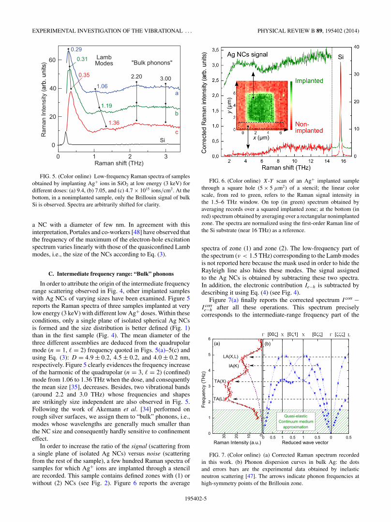
FIG. 5. (Color online) Low-frequency Raman spectra of samplesobtained by implanting Ag+ ions in SiO2 at low energy (3 keV) fordifferent doses: (a) 9.4, (b) 7.05, and (c) 4.7 × 10¹⁵ ions/cm2. At thebottom, in a nonimplanted sample, only the Brillouin signal of bulkSi is observed. Spectra are arbitrarily shifted for clarity.
a NC with a diameter of few nm. In agreement with thisinterpretation, Portales and co-workers [48] have observed thatthe frequency of the maximum of the electron-hole excitationspectrum varies linearly with those of the quasiconfined Lambmodes, i.e., the size of the NCs according to Eq. (3).
C. Intermediate frequency range: “Bulk” phonons
In order to attribute the origin of the intermediate frequencyrange scattering observed in Fig. 4, other implanted sampleswith Ag NCs of varying sizes have been examined. Figure 5reports the Raman spectra of three samples implanted at verylow energy (3 keV) with different low Ag+ doses. Within theseconditions, only a single plane of isolated spherical Ag NCsis formed and the size distribution is better defined (Fig. 1)than in the first sample (Fig. 4). The mean diameter of thethree different assemblies are deduced from the quadrupolarmode (n = 1, � = 2) frequency quoted in Figs. 5(a)–5(c) andusing Eq. (3): D = 4.9 ± 0.2, 4.5 ± 0.2, and 4.0 ± 0.2 nm,respectively. Figure 5 clearly evidences the frequency increaseof the harmonic of the quadrupolar (n = 3, � = 2) (confined)mode from 1.06 to 1.36 THz when the dose, and consequentlythe mean size [35], decreases. Besides, two vibrational bands(around 2.2 and 3.0 THz) whose frequencies and shapesare strikingly size independent are also observed in Fig. 5.Following the work of Akemann et al. [34] performed onrough silver surfaces, we assign them to “bulk” phonons, i.e.,modes whose wavelengths are generally much smaller thanthe NC size and consequently hardly sensitive to confinementeffect.
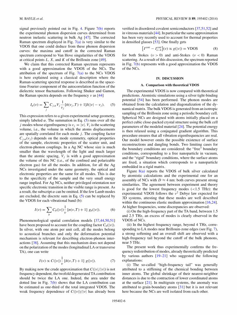
In order to increase the ratio of the signal (scattering froma single plane of isolated Ag NCs) versus noise (scatteringfrom the rest of the sample), a few hundred Raman spectra ofsamples for which Ag+ ions are implanted through a stencilare recorded. This sample contains defined zones with (1) orwithout (2) NCs (see Fig. 2). Figure 6 reports the average
FIG. 6. (Color online) X-Y scan of an Ag+ implanted samplethrough a square hole (5 × 5 μm2) of a stencil; the linear colorscale, from red to green, refers to the Raman signal intensity inthe 1.5–6 THz window. On top (in green) spectrum obtained byaveraging records over a squared implanted zone; at the bottom (inred) spectrum obtained by averaging over a rectangular nonimplantedzone. The spectra are normalized using the first-order Raman line ofthe Si substrate (near 16 THz) as a reference.
spectra of zone (1) and zone (2). The low-frequency part ofthe spectrum (ν < 1.5 THz) corresponding to the Lamb modesis not reported here because the mask used in order to hide theRayleigh line also hides these modes. The signal assignedto the Ag NCs is obtained by subtracting these two spectra.In addition, the electronic contribution Ie−h is subtracted bydescribing it using Eq. (4) (see Fig. 4).
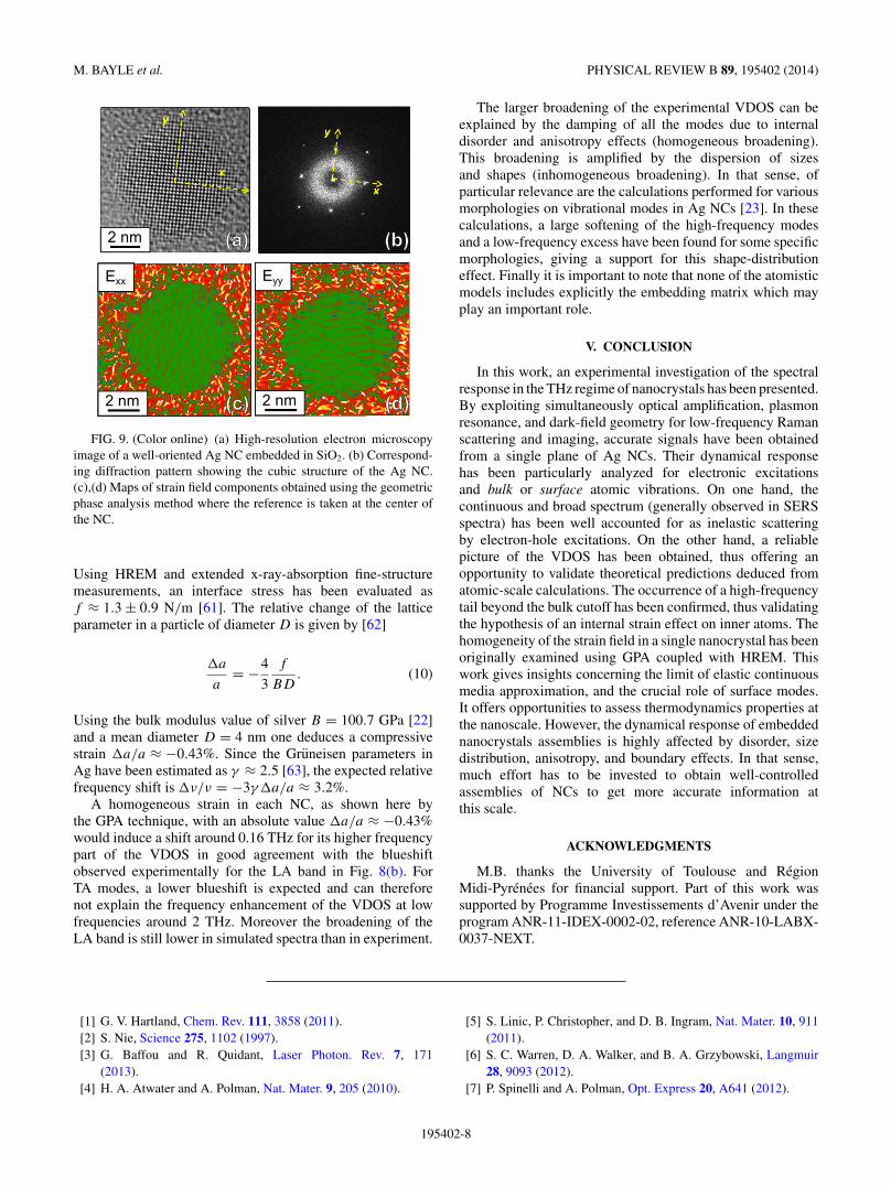
Figure 7(a) finally reports the corrected spectrum I corr −I corre−h after all these operations. This spectrum precisely
corresponds to the intermediate-range frequency part of the
FIG. 7. (Color online) (a) Corrected Raman spectrum recordedin this work. (b) Phonon dispersion curves in bulk Ag: the dotsand errors bars are the experimental data obtained by inelasticneutron scattering [47]. The arrows indicate phonon frequencies athigh-symmetry points of the Brillouin zone.
195402-5
M. BAYLE et al. PHYSICAL REVIEW B 89, 195402 (2014)
signal previously pointed out in Fig. 4. Figure 7(b) reportsthe experimental phonon dispersion curves determined fromneutron inelastic scattering in bulk Ag [47]. The correctedRaman spectrum displayed in Fig. 7(a) is very similar to theVDOS that one could deduce from these phonon dispersioncurves: the maxima and cutoff in the corrected Ramanspectrum correspond to Van Hove singularities of the VDOSat critical points L, X, and K of the Brillouin zone [49].
We claim that this corrected Raman spectrum representswith a good approximation the VDOS of the NCs. Theattribution of the spectrum of Fig. 7(a) to the NCs VDOSis here explained using a classical description where theRaman-scattering spectral response is described as the space-time Fourier component of the autocorrelation function of thedielectric tensor fluctuations. Following Shuker and Gamon,the Raman spectra depends on the frequency ν as [44]
Iα(ν) =∑
j
Cj,αVj
1
νj
[n(νj ,T ) + 1]δ(|ν| − νj ). (5)
This expression refers to a given experimental setup geometry,simply labeled α. The summation in Eq. (5) runs over all thej modes whose eigenfrequency is νj = |ν|. Vj is the scatteringvolume, i.e., the volume in which the atoms displacementsare spatially correlated for each mode j . The coupling factorCj,α(νj ) depends on the mode symmetry, optical propertiesof the sample, electronic properties of the scatter unit, andelectron-phonon couplings. In a Ag NC whose size is muchsmaller than the wavelength of the light and much largerthan the atomic spacing, Vj is with a good approximationthe volume of this NC (i.e., of the confined and polarizableelectron gas) for all the modes. In addition, for all the AgNCs investigated under the same geometry, the optical andelectronic properties are the same for all modes. This is dueto the specificity of the sample and the very small energyrange implied. For Ag NCs, neither privileged orientation norspecific electronic transition in the visible range is present. Asa result, the subscript α can be omitted. If the few Lamb modesare excluded, the discrete sum in Eq. (5) can be replaced bythe VDOS for each vibrational band (b):
I (ν) =∑
b
Cb(|ν|) 1
ν[n(ν,T ) + 1] gb(|ν|). (6)
Phenomenological spatial correlation models [37,44,50,51]have been proposed to account for the coupling factor Cb(|ν|).In silver, with one atom per unit cell, all the modes belongto acoustical branches and only the deformation potentialmechanism is relevant for describing electron-phonon inter-actions [38]. Assuming that this mechanism does not dependon the polarization of the modes (longitudinal LA or transverseTA), one can write
I (ν) ∝ C(|ν|) 1
ν[n(ν,T ) + 1] g(|ν|). (7)
By making now the crude approximation that C(|ν|/|ν|) is notfrequency dependent, the twofold degenerated TA contributionshould be twice the LA one. Indeed, the area under thedotted line in Fig. 7(b) shows that the LA contribution canbe estimated as one-third of the total integrated VDOS. Theweak frequency dependence of C(|ν|)/|ν| has already been
verified in disordered covalent semiconductors [37,51,52] andin vitreous materials [44]. In particular the same approximationhas been very recently used to account for thermal propertiesin densified glasses [53]. One finally gets[
I corr − I corre−h
](ν) ∝ g(|ν|) = VDOS (8)
for both Stokes (ν > 0) and anti-Stokes (ν < 0) Ramanscattering. As a result of this discussion, the spectrum reportedin Fig. 7(b) represents with a good approximation the VDOSof the NCs.
IV. DISCUSSION
A. Comparison with theoretical VDOS
The experimental VDOS is now compared with theoreticalpredictions. Atomistic simulations using a silver tight-bindingpotential [54] has been performed. The phonon modes areobtained from the calculation and diagonalization of the dy-namical matrix. The bulk VDOS is generated from an isotropicsampling of the Brillouin zone using a periodic boundary cell.Spherical NCs are designed with atoms initially placed on aperfect cubic close-packed crystal structure using the bulk cellparameters of the modeled material [24]. The potential energyis then relaxed using a conjugated gradient algorithm. Thisprocedure ensures that all vibration eigenfrequencies are real.Our model however omits the possible existence of surfacereconstructions and dangling bonds. Two limiting cases forthe boundary conditions are considered: the “free” boundaryconditions, corresponding to a free nanoparticle in vacuum,and the “rigid” boundary conditions, where the surface atomsare fixed, a situation which corresponds to a nanoparticleembedded in a rigid matrix.
Figure 8(a) reports the VDOS of bulk silver calculatedby atomistic calculations and the experimental one for anassembly of NCs with D ≈ 4 nm: both curves present strongsimilarities. The agreement between experiment and theoryis good for the lowest frequency modes (<1.5 THz): theexperimental VDOS follows the ν2 Debye law expected for3D systems, attesting that these modes are well describedwithin the continuous elastic medium approximation [16,24].At higher frequencies, some discrepancies are observed:
(i) On the high-frequency part of the TA band, between 1.5and 2.5 THz, an excess of modes is clearly observed in theVDOS of NCs.
(ii) In the highest frequency range, beyond 4 THz, corre-sponding to LA modes near Brillouin-zone edges (see Fig. 7),a strong softening and an overall shift are observed with ahigh-frequency tail beyond the cutoff of the bulk phonons,near 5 THz.
The present work thus experimentally confirms the fre-quency redistribution of modes, already theoretically predictedby various authors [19–21] who suggested the followingexplanations:
(i) The so-called “high-frequency tail” was generallyattributed to a stiffening of the chemical bonding betweeninner atoms. The global shrinkage of their nearest-neighbordistances is due to the contraction of lower coordinated atomsat the surface [21]. In multigrain systems, the anomaly wasattributed to grain-boundary atoms [31] but it is not relevanthere because the NCs are well isolated from each other.
195402-6

EXPERIMENTAL INVESTIGATION OF THE VIBRATIONAL . . . PHYSICAL REVIEW B 89, 195402 (2014)
FIG. 8. (Color online) (a) Comparison of VDOS calculated forbulk Ag using atomic-scale simulations (continuous black line)and for an assembly of Ag NCs (mean size D ≈ 4 nm) obtainedexperimentally (red dots); (b) Calculated VDOS of a spherical NCwith 2072 atoms Ag atoms (D = 4 nm) for free and rigid boundaryconditions, and of a NC with 555 atoms. All the integrated areas havebeen normalized.
(ii) The “low-frequency excess” was attributed to vibrationsof undercoordinated surface atoms characterized by a differentbinding. The enhancement of the VDOS at very low frequency(Debye regime) could then be explained by a reduction ofdimensionality leading to a change on frequency dependencefrom quadratic (3D for volume modes) to linear (2D for surfacemodes).
B. Size, strain, and disorder effects
In order to analyze more precisely these effects, we have onone hand calculated the VDOS of a 4-nm-diameter sphericalAg NC for two opposite boundary conditions, free or rigid,and on the other hand checked experimentally the strain fieldin isolated NCs.
Figure 8(b) reports the VDOS of a NC with 2072 atoms Agatoms (D = 4 nm) for both free and rigid boundary conditions.The low-frequency excess (i) and the high-frequency tail (ii)are clearly visible in both cases but they are more pronouncedin the free boundary conditions case, demonstrating thatdisplacements of Ag surface atoms play a significant role.As a matter of fact one observes in Fig. 8(b) that increasingthe surface-to-volume ratio by reducing the size of the NCto 555 atoms (D = 2.65 nm) does enhance both low- andhigh-frequency anomalies.
The frequency redistribution of vibrational modes inNCs is at the origin of the modification of thermodynamic
properties [19–21], namely the lattice specific heat Cv[22]:
Cv = kB
∫ ∞
0g(ν)
(hν
kBT
)2ehν/kBT
(ehν/kBT − 1)2dν. (9)
The Debye approximation consists of using in Eq. (9), for 0 �ν � kBTD/h, the following expression of the VDOS, gD(ν) =18πNa(h/kBTD)3ν2, where TD is the Debye temperature.Using Eq. (9) and the bulk and NC VDOS reported in Fig. 8,an effective Debye temperature is determined by fitting thecalculated Cv(T ) curves with the Debye function Cv,D(T ). Inthis Debye function, we used the expression of gD(ν) with TD
as the only adjustable parameter. From the atomic simulationof bulk Ag, one finds TD = 210 ± 3 K in good agreement withthe experiment (215 K) [22]. Simulations of NCs with freeboundaries conditions yield TD = 205 K. The experimentalVDOS extracted from the Raman spectrum can be also usedin Eq. (9) to analyze the thermal behavior [53]. In our case, thebest fit is obtained with TD = 195 K: this gives a confirmationof the lowering of TD with the size reduction, as predictedtheoretically [20].
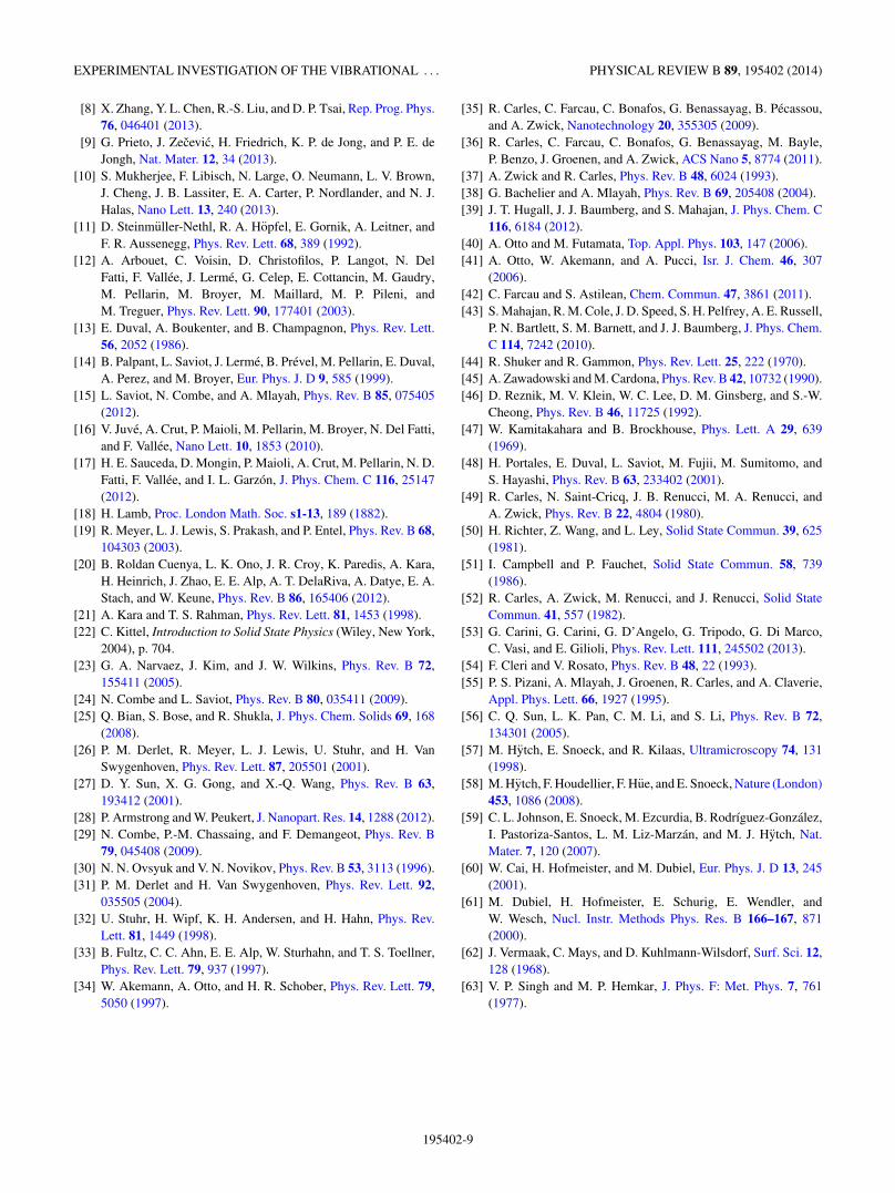
Internal strain effects have been already examined ex-perimentally using simulations to account for vibrationalfrequency shifts in NCs [28,55,56]. Because strain inhomo-geneity may induce broadening, we have performed strainmapping of Ag NCs by analyzing their high-resolution electronmicroscopy (HREM) images using the geometrical phaseanalysis (GPA) technique [57]. This technique has been widelyused for strain measurements in epitaxial layers or MOSdevices [58] but only a few studies concern strain in smallnanocrystals [59]. The GPA technique consists of decompos-ing a HREM image in the Fourier space and analyzing theFourier components of two spatial frequencies correspondingto two systems of periodic fringes in the direct space.From the geometric phase variations of noncollinear Fouriercomponents, the local changes of periodicity are deduced bycomparison with an unstrained reference zone. The spatialanalysis of these periodicity variations provides the mappingof strains, rotations, and shears of the strained structure in theobservation plane. The GPA technique measures these phaseshifts and maps the strain in “small” crystalline zones (withinfew tens of nm) with respect to a region taken as a reference(i.e., unstrained) with accuracy of 0.1% and subnanometricspatial resolution. Cross-sectional and plan-view specimenswere prepared for TEM examination by the tripod methodand finished by a gentle ion milling step. A FEI Tecnaimicroscope equipped with a field emission gun and a sphericalaberration corrector and operating at 200 keV was used forimaging.
The strain field inside an embedded nanocrystal (see Fig. 9)is found to be homogeneous (standard deviation less than0.1%). The same conclusion is confirmed by examining severalNCs. However the spatial resolution of the GPA techniqueremains around 0.7 nm for the images shown in Fig. 9 and thussurface effects at the atomic scale cannot be analyzed. Absolutemeasurements of this homogeneous strain would have requireda time-consuming statistical study and the use of an outsidereference (such as the Si substrate). We simply refer here toalready published data by Hofmeister and co-workers [60,61]on assemblies of Ag NCs obtained by implantation in SiO2.
195402-7
M. BAYLE et al. PHYSICAL REVIEW B 89, 195402 (2014)
FIG. 9. (Color online) (a) High-resolution electron microscopyimage of a well-oriented Ag NC embedded in SiO2. (b) Correspond-ing diffraction pattern showing the cubic structure of the Ag NC.(c),(d) Maps of strain field components obtained using the geometricphase analysis method where the reference is taken at the center ofthe NC.
Using HREM and extended x-ray-absorption fine-structuremeasurements, an interface stress has been evaluated asf ≈ 1.3 ± 0.9 N/m [61]. The relative change of the latticeparameter in a particle of diameter D is given by [62]
�a
a= −4
3
f
BD. (10)
Using the bulk modulus value of silver B = 100.7 GPa [22]and a mean diameter D = 4 nm one deduces a compressivestrain �a/a ≈ −0.43%. Since the Gruneisen parameters inAg have been estimated as γ ≈ 2.5 [63], the expected relativefrequency shift is �ν/ν = −3γ�a/a ≈ 3.2%.
A homogeneous strain in each NC, as shown here bythe GPA technique, with an absolute value �a/a ≈ −0.43%would induce a shift around 0.16 THz for its higher frequencypart of the VDOS in good agreement with the blueshiftobserved experimentally for the LA band in Fig. 8(b). ForTA modes, a lower blueshift is expected and can thereforenot explain the frequency enhancement of the VDOS at lowfrequencies around 2 THz. Moreover the broadening of theLA band is still lower in simulated spectra than in experiment.
The larger broadening of the experimental VDOS can beexplained by the damping of all the modes due to internaldisorder and anisotropy effects (homogeneous broadening).This broadening is amplified by the dispersion of sizesand shapes (inhomogeneous broadening). In that sense, ofparticular relevance are the calculations performed for variousmorphologies on vibrational modes in Ag NCs [23]. In thesecalculations, a large softening of the high-frequency modesand a low-frequency excess have been found for some specificmorphologies, giving a support for this shape-distributioneffect. Finally it is important to note that none of the atomisticmodels includes explicitly the embedding matrix which mayplay an important role.
V. CONCLUSION
In this work, an experimental investigation of the spectralresponse in the THz regime of nanocrystals has been presented.By exploiting simultaneously optical amplification, plasmonresonance, and dark-field geometry for low-frequency Ramanscattering and imaging, accurate signals have been obtainedfrom a single plane of Ag NCs. Their dynamical responsehas been particularly analyzed for electronic excitationsand bulk or surface atomic vibrations. On one hand, thecontinuous and broad spectrum (generally observed in SERSspectra) has been well accounted for as inelastic scatteringby electron-hole excitations. On the other hand, a reliablepicture of the VDOS has been obtained, thus offering anopportunity to validate theoretical predictions deduced fromatomic-scale calculations. The occurrence of a high-frequencytail beyond the bulk cutoff has been confirmed, thus validatingthe hypothesis of an internal strain effect on inner atoms. Thehomogeneity of the strain field in a single nanocrystal has beenoriginally examined using GPA coupled with HREM. Thiswork gives insights concerning the limit of elastic continuousmedia approximation, and the crucial role of surface modes.It offers opportunities to assess thermodynamics properties atthe nanoscale. However, the dynamical response of embeddednanocrystals assemblies is highly affected by disorder, sizedistribution, anisotropy, and boundary effects. In that sense,much effort has to be invested to obtain well-controlledassemblies of NCs to get more accurate information atthis scale.
ACKNOWLEDGMENTS
M.B. thanks the University of Toulouse and RegionMidi-Pyrenees for financial support. Part of this work wassupported by Programme Investissements d’Avenir under theprogram ANR-11-IDEX-0002-02, reference ANR-10-LABX-0037-NEXT.
[1] G. V. Hartland, Chem. Rev. 111, 3858 (2011).[2] S. Nie, Science 275, 1102 (1997).[3] G. Baffou and R. Quidant, Laser Photon. Rev. 7, 171
(2013).[4] H. A. Atwater and A. Polman, Nat. Mater. 9, 205 (2010).
[5] S. Linic, P. Christopher, and D. B. Ingram, Nat. Mater. 10, 911(2011).
[6] S. C. Warren, D. A. Walker, and B. A. Grzybowski, Langmuir28, 9093 (2012).
[7] P. Spinelli and A. Polman, Opt. Express 20, A641 (2012).
195402-8
EXPERIMENTAL INVESTIGATION OF THE VIBRATIONAL . . . PHYSICAL REVIEW B 89, 195402 (2014)
[8] X. Zhang, Y. L. Chen, R.-S. Liu, and D. P. Tsai, Rep. Prog. Phys.76, 046401 (2013).
[9] G. Prieto, J. Zecevic, H. Friedrich, K. P. de Jong, and P. E. deJongh, Nat. Mater. 12, 34 (2013).
[10] S. Mukherjee, F. Libisch, N. Large, O. Neumann, L. V. Brown,J. Cheng, J. B. Lassiter, E. A. Carter, P. Nordlander, and N. J.Halas, Nano Lett. 13, 240 (2013).
[11] D. Steinmuller-Nethl, R. A. Hopfel, E. Gornik, A. Leitner, andF. R. Aussenegg, Phys. Rev. Lett. 68, 389 (1992).
[12] A. Arbouet, C. Voisin, D. Christofilos, P. Langot, N. DelFatti, F. Vallee, J. Lerme, G. Celep, E. Cottancin, M. Gaudry,M. Pellarin, M. Broyer, M. Maillard, M. P. Pileni, andM. Treguer, Phys. Rev. Lett. 90, 177401 (2003).
[13] E. Duval, A. Boukenter, and B. Champagnon, Phys. Rev. Lett.56, 2052 (1986).
[14] B. Palpant, L. Saviot, J. Lerme, B. Prevel, M. Pellarin, E. Duval,A. Perez, and M. Broyer, Eur. Phys. J. D 9, 585 (1999).
[15] L. Saviot, N. Combe, and A. Mlayah, Phys. Rev. B 85, 075405(2012).
[16] V. Juve, A. Crut, P. Maioli, M. Pellarin, M. Broyer, N. Del Fatti,and F. Vallee, Nano Lett. 10, 1853 (2010).
[17] H. E. Sauceda, D. Mongin, P. Maioli, A. Crut, M. Pellarin, N. D.Fatti, F. Vallee, and I. L. Garzon, J. Phys. Chem. C 116, 25147(2012).
[18] H. Lamb, Proc. London Math. Soc. s1-13, 189 (1882).[19] R. Meyer, L. J. Lewis, S. Prakash, and P. Entel, Phys. Rev. B 68,
104303 (2003).[20] B. Roldan Cuenya, L. K. Ono, J. R. Croy, K. Paredis, A. Kara,
H. Heinrich, J. Zhao, E. E. Alp, A. T. DelaRiva, A. Datye, E. A.Stach, and W. Keune, Phys. Rev. B 86, 165406 (2012).
[21] A. Kara and T. S. Rahman, Phys. Rev. Lett. 81, 1453 (1998).[22] C. Kittel, Introduction to Solid State Physics (Wiley, New York,
2004), p. 704.[23] G. A. Narvaez, J. Kim, and J. W. Wilkins, Phys. Rev. B 72,
155411 (2005).[24] N. Combe and L. Saviot, Phys. Rev. B 80, 035411 (2009).[25] Q. Bian, S. Bose, and R. Shukla, J. Phys. Chem. Solids 69, 168
(2008).[26] P. M. Derlet, R. Meyer, L. J. Lewis, U. Stuhr, and H. Van
Swygenhoven, Phys. Rev. Lett. 87, 205501 (2001).[27] D. Y. Sun, X. G. Gong, and X.-Q. Wang, Phys. Rev. B 63,
193412 (2001).[28] P. Armstrong and W. Peukert, J. Nanopart. Res. 14, 1288 (2012).[29] N. Combe, P.-M. Chassaing, and F. Demangeot, Phys. Rev. B
79, 045408 (2009).[30] N. N. Ovsyuk and V. N. Novikov, Phys. Rev. B 53, 3113 (1996).[31] P. M. Derlet and H. Van Swygenhoven, Phys. Rev. Lett. 92,
035505 (2004).[32] U. Stuhr, H. Wipf, K. H. Andersen, and H. Hahn, Phys. Rev.
Lett. 81, 1449 (1998).[33] B. Fultz, C. C. Ahn, E. E. Alp, W. Sturhahn, and T. S. Toellner,
Phys. Rev. Lett. 79, 937 (1997).[34] W. Akemann, A. Otto, and H. R. Schober, Phys. Rev. Lett. 79,
5050 (1997).
[35] R. Carles, C. Farcau, C. Bonafos, G. Benassayag, B. Pecassou,and A. Zwick, Nanotechnology 20, 355305 (2009).
[36] R. Carles, C. Farcau, C. Bonafos, G. Benassayag, M. Bayle,P. Benzo, J. Groenen, and A. Zwick, ACS Nano 5, 8774 (2011).
[37] A. Zwick and R. Carles, Phys. Rev. B 48, 6024 (1993).[38] G. Bachelier and A. Mlayah, Phys. Rev. B 69, 205408 (2004).[39] J. T. Hugall, J. J. Baumberg, and S. Mahajan, J. Phys. Chem. C
116, 6184 (2012).[40] A. Otto and M. Futamata, Top. Appl. Phys. 103, 147 (2006).[41] A. Otto, W. Akemann, and A. Pucci, Isr. J. Chem. 46, 307
(2006).[42] C. Farcau and S. Astilean, Chem. Commun. 47, 3861 (2011).[43] S. Mahajan, R. M. Cole, J. D. Speed, S. H. Pelfrey, A. E. Russell,
P. N. Bartlett, S. M. Barnett, and J. J. Baumberg, J. Phys. Chem.C 114, 7242 (2010).
[44] R. Shuker and R. Gammon, Phys. Rev. Lett. 25, 222 (1970).[45] A. Zawadowski and M. Cardona, Phys. Rev. B 42, 10732 (1990).[46] D. Reznik, M. V. Klein, W. C. Lee, D. M. Ginsberg, and S.-W.
Cheong, Phys. Rev. B 46, 11725 (1992).[47] W. Kamitakahara and B. Brockhouse, Phys. Lett. A 29, 639
(1969).[48] H. Portales, E. Duval, L. Saviot, M. Fujii, M. Sumitomo, and
S. Hayashi, Phys. Rev. B 63, 233402 (2001).[49] R. Carles, N. Saint-Cricq, J. B. Renucci, M. A. Renucci, and
A. Zwick, Phys. Rev. B 22, 4804 (1980).[50] H. Richter, Z. Wang, and L. Ley, Solid State Commun. 39, 625
(1981).[51] I. Campbell and P. Fauchet, Solid State Commun. 58, 739
(1986).[52] R. Carles, A. Zwick, M. Renucci, and J. Renucci, Solid State
Commun. 41, 557 (1982).[53] G. Carini, G. Carini, G. D’Angelo, G. Tripodo, G. Di Marco,
C. Vasi, and E. Gilioli, Phys. Rev. Lett. 111, 245502 (2013).[54] F. Cleri and V. Rosato, Phys. Rev. B 48, 22 (1993).[55] P. S. Pizani, A. Mlayah, J. Groenen, R. Carles, and A. Claverie,
Appl. Phys. Lett. 66, 1927 (1995).[56] C. Q. Sun, L. K. Pan, C. M. Li, and S. Li, Phys. Rev. B 72,
134301 (2005).[57] M. Hytch, E. Snoeck, and R. Kilaas, Ultramicroscopy 74, 131
(1998).[58] M. Hytch, F. Houdellier, F. Hue, and E. Snoeck, Nature (London)
453, 1086 (2008).[59] C. L. Johnson, E. Snoeck, M. Ezcurdia, B. Rodrıguez-Gonzalez,
I. Pastoriza-Santos, L. M. Liz-Marzan, and M. J. Hytch, Nat.Mater. 7, 120 (2007).
[60] W. Cai, H. Hofmeister, and M. Dubiel, Eur. Phys. J. D 13, 245(2001).
[61] M. Dubiel, H. Hofmeister, E. Schurig, E. Wendler, andW. Wesch, Nucl. Instr. Methods Phys. Res. B 166–167, 871(2000).
[62] J. Vermaak, C. Mays, and D. Kuhlmann-Wilsdorf, Surf. Sci. 12,128 (1968).
[63] V. P. Singh and M. P. Hemkar, J. Phys. F: Met. Phys. 7, 761(1977).
195402-9