Embed Size (px)
Citation preview

The Pennsylvania State University
The Graduate School
EXPERIMENTAL AND SIMULATED STUDY OF FLEXIBLE ELECTRONICS
--FABRICATION OF WATER-SOLUBLE ZN/PVA SENSOR AND STRETCHING
SIMULATION OF GNM/SWNT
A Thesis in
Engineering Science and Mechanics
by
Yuyan Gao
© 2020 Yuyan Gao
Submitted in Partial Fulfillment
of the Requirements
for the Degree of
Master of Science
May 2020

ii
The thesis of Yuyan Gao was reviewed and approved* by the following:
Huanyu (Larry) Cheng
Assistant Professor of Engineering Science and Mechanics
Thesis Adviser
Clifford Lissenden
Professor of Engineering Science and Mechanics
Jian Hsu
Professor of Engineering Science and Mechanics
Judith Todd
Professor of Engineering Science and Mechanics
Head of the Department of Engineering Science and Mechanics

iii
ABSTRACT
Flexible electronics are broadly studied for the potential in wearable devices. Transient and
flexible electronics for human health monitoring are promising because this kind of electronics
can be implantable and zero-waste after use. Transient electronics are commonly fabricated in the
cleanroom. The process is time-consuming and costly. Photonic sintering method occurred in
recent years and it provides a fast, cheap and low-temperature way of fabrication about transient
electronics. This study takes advantage of photonic sintering technique to fabricate fully
dissolvable PVA/Zn ECG sensor, EMG sensor and temperature sensor. Different substrates are
utilized for ECG sensor and their performance are compared. The dissolution of electrodes in the
water is also studied. In order to study the mechanical properties of flexible electronics, the
simulation about stretching of porous graphene/carbon nanotube is also studied. The stress and
strain contour of the stretched bilayer structure is obtained indicating a better tensile stiffness of
the composite.

iv
TABLE OF CONTENTS
LIST OF FIGURES ........................................................................................................................ v LIST OF TABLES ......................................................................................................................... vi ACKNOWLEDGEMENT ............................................................................................................ vii Chapter 1 Background & introduction ............................................................................................ 1
1.1 Flexible electronics ....................................................................................................... 1
1.2 Transient flexible electronics ........................................................................................ 2
1.3 Photonic sintering ......................................................................................................... 4 Chapter 2. Fabrication method ........................................................................................................ 6
2.1 Preparation of PVA solution ......................................................................................... 6
2.2 Preparation of PVA membrane ..................................................................................... 7
2.3 Preparation of zinc/ethanol ink ..................................................................................... 7
2.4 Preparation of Zn/PI film .............................................................................................. 8
2.5 Transfer printing of Zn/PVA membrane..................................................................... 10
Chapter 3. Results and discussion ................................................................................................. 13
3.1 Scanning electron microscope (SEM) images ............................................................ 13
3.2 Size effect of electrodes for surface electric resistance .............................................. 14
3.3 The change of electric resistance under strain ............................................................ 15
3.4 ECG signals ................................................................................................................ 16
3.5 Electromyography (EMG) signals .............................................................................. 25
3.6 Zn/PVA membrane as temperature sensor ................................................................. 28
3.7 Dissolving properties .................................................................................................. 30 Chapter 4 Finite element analysis of graphene-nanomesh (GNM)/single wall carbon-nanotube
(SWNT) hybrid membrane ........................................................................................................... 32
4.1 Finite element analysis of the SWNT network ........................................................... 33
4.2 Analysis of the mechanical performance of GNM structure ...................................... 34
4.4 Bending stiffness of GNM and GNM/SWNT membrane........................................... 37
Chapter 5 Conclusion .................................................................................................................... 39 References ..................................................................................................................................... 40

v
LIST OF FIGURES
Figure 1.1 Chemical structure of PVA: (A) partially hydrolyzed; (B) fully hydrolyzed ............... 3
Figure 2.1 Preparation of PVA solution ......................................................................................... 6
Figure 2.2 film applicator and preparation of PVA membrane. ..................................................... 7
Figure 2.3 zinc/ethanol ink ............................................................................................................. 8
Figure 2.4 UV Ozone system .......................................................................................................... 9
Figure 2.5 Dried Zinc nanoparticles on PI films ........................................................................... 10
Figure 2.6 Schematic illustration of transfer printing process ...................................................... 10
Figure 2.7 The XENON X-1100 photonic sintering system......................................................... 11
Figure 2.8 Parameter setting screen of X-1100 photonic sintering system .................................. 12
Figure 3.1 SEM image of Zn nanoparticles before and after photonic sintering .......................... 13
Figure 3.2 SEM image of PVA membrane before and after attaching to skin ............................. 14
Figure 3.3 Electric resistance change vs length change of electrodes .......................................... 15
Figure 3.4 Electric resistance change with respect to strain ......................................................... 16
Figure 3.5 (A)PVA/Zn electrode for ECG sensor; (B) commercial gel electrodes ...................... 17
Figure 3.6 Schematic demonstration of simplified equivalent circuit between the electrode and
skin ................................................................................................................................................ 18
Figure 3.7 Contact impedance change vs frequency. The red line indicates PVA/Zn electrode and
the black line shows the commercial gel electrode. ...................................................................... 19
Figure 3.8 Demonstration of P,QRS,T wave and Vs, Vn amplitude of an ECG signal. .............. 20
Figure 3.9 Simultaneous ECG signal from Zn/ PVA electrodes and commercial gel electrodes 21
Figure 3.10 ECG signal from water soluble tape/Zn electrode. ................................................... 22
Figure 3.11 Schematic fabrication process for electrospinning. ................................................... 22
Figure 3.12 (A) ECG signal from electrospun PVA/Zn nanomesh electrodes (blue line) and (B)
ECG signal from commercial gel electrodes (red line) ................................................................ 24
Figure 3.13 weight loss of water evaporation with time. .............................................................. 25
Figure 3.15 (A) EMG signal from PVA/Zn electrode (blue line) and (B) EMG signal from
commercial gel electrode (red line). ............................................................................................. 27
Figure 3.16 Patterned Zn/PVA membrane as temperature sensor ................................................ 29
Figure 3.17 Electric resistance change vs temperature change of the PVA/Zn temperature sensor
....................................................................................................................................................... 30
Figure 3.18 demonstration of dissolving PVA/Zn electrode in 90 0C water. ............................... 31
Figure 4.1Geometry of SWNT membrane in the simulation model ............................................. 34
Figure 4.2 geometry of porous GNM in the simulation model..................................................... 35
Figure 4.3 Mises stress contour of GNM/SWNT membrane after 5% stretching ........................ 36
Figure 4.4 Strain contour of GNM/SWNT membrane after 5% stretching .................................. 37

vi
LIST OF TABLES
Table 1. Various functions for lab-on-skin electronics ................................................................... 1
Table 2. Dissolution rate in DI water for different metal material [23] .......................................... 3

vii
ACKNOWLEDGEMENT
I would like to thank Dr. Huanyu Cheng for his guide and help in this program. I would also thank
Ning Yi and Jia Zhu, two doctoral students in Dr. Cheng’s lab, for their help in experiments. I
appreciate supports from my parents.

1
Chapter 1 Background & introduction
1.1 Flexible electronics
Flexible electronics are a kind of electronics that can function well under folding or twisting modes.
Flexible electronics are typically composed of two layers: one thin substrate and one functional
electronic component. In some cases, there also exist one encapsulation layer. Flexible electronics
have a wide range of applications include flexible circuit [1], flexible displays [2], flexible solar
cells [3], implantable medical sensors [4] and lab-on-skin electronics [5].
Flexible electronics have advantages in lab-on-skin electronics for conformability and flexibility
since human skin is soft, flexible and stretchable. Table 1 shows various kinds of lab-on-skin
electronics that have different functions like sensing EEG, ECG, EMG signal, temperature, strain
and hydration from human skin for better health monitoring.
Table 1. Various functions for lab-on-skin electronics
References Functions
Ref. [6-8] EEG, ECG, EMG signal sensor
Ref. [9, 10] Temperature sensor
Ref. [11, 12] Sweat sensor
Ref. [13, 14] Strain sensor
Ref. [11, 14] Hydration sensor
Ref. [15, 16] Pressure sensor

2
1.2 Transient flexible electronics
Transient electronics are a class of electronics that can dissolve into certain liquids, like biofluid
or water after stable operation for a period of time. Transient and flexible electronics have specific
need in temporary biomedical implants [17-20]. It can be designed as biodegradable electronics
onto human body for health monitoring sensing. It can be brain sensors to measure intracranial
pressure and temperature [21]. It can also work as transient spatiotemporal mapping of electrical
activity from the cerebral cortex [22]. No byproduct remains and no second surgery needs for the
implant transient electronics after use. Transient electronics usually consist of semiconductors,
conductors, dielectrics, and substrate.
Metal layer serve as conductor and interconnection. Metals have higher electric conductivity than
conductive polymer. Magnesium (Mg), Zinc (Zn), Iron (Fe), Molybdenum (Mo) and Tungsten
(W) are dissolvable metals for transient electronics. Mg, Zn, Fe and Mo are micronutrients and
they are important for human body[23]. Mg, Fe and their alloys can be used as bioimplants [24-
26]. The dissolvable rate of different metals are different: Mg dissolves in a simulated body fluids
(SBFs) at 0.05-0.5 μm/h and Fe dissolves at a rate of 0.2μm/h [23]. Dissolution rate in DI water
for various kinds of metals can be found in table 2 [23]. We can observe from the table 2 that
dissolution rate of Mg and Zn are quicker than the rate of W and Mn. By selection of different
metals, different level of dissolution requirement can be satisfied.

3
Table 2. Dissolution rate in DI water for different metal material [23]
Material Dissolution rate in DI water (μm/h) References
Mg 0.07 Ref. [23, 27]
Mg AZ31B alloy 0.02 Ref. [28]
Sputtered W 1.7x10⁻³ Ref. [29]
CVD W 3x10⁻⁴ Ref. [29]
Mo 3x10⁻⁴ Ref. [30]
Zn 7x10⁻³ Ref. [31]
Many water-soluble polymers contain hydrophilic groups so that they can dissolve into water.
Common water-soluble substrate include poly(vinyl alcohol) (PVA), polyvinylpyrrolidone (PVP)
and polylacticcoglycolic acid (PLGA) [18]. Polyvinyl alcohol (PVA) is a water-soluble,
biodegradable and biocompatible synthetic polymer that is widely used in wound dressings, drug
delivery, implants and artificial organs [32]. PVA/starch blends are widely used in packaging [33].
Figure 1.1 is the chemical structure of PVA polymer under partially hydrolyzed state and fully
hydrolyzed state.
Figure 1.1 Chemical structure of PVA: (A) partially hydrolyzed; (B) fully hydrolyzed

4
For the semiconductors in transient electronics, silicon is widely used in electronic industry. Since
silicon can dissolve in water through hydrolysis, monocrystalline silicon nanomembranes and
silicon oxide are applied in transient electronics [34].
1.3 Photonic sintering
Photonic sintering or photonic curing is a technology that can sinter metal nanoparticles like Cu,
Ag and Zn in millisecond level. The working principle is as follows: a broad-spectrum light is
introduced onto the target nanoparticles and the energy of optical light converts into heat of
nanoparticles. Nanoparticles then merge together to form a conductive layer. Photonic sintering
has many advantages. It is a fast process that can generate conductive layer within milliseconds.
Since the exposure period of light is short, photonic sintering is also a low-temperature fabrication
procedure that will not damage the thermal sensitive substrate. It is also a cheap process. Large
area sintering can be achieved by roll-to-roll light sintering. The broad spectrum of xenon light
makes it possible to sinter a variety of nanoparticles.
In order to compare the performance of photonic sintering and thermal sintering, current collecting
grids by inkjet printing for organic solar cells are sintered by thermal treatment and photonic
sintering [35]. It shows that similar conductivities are achieved by 5 seconds of photonic sintering
and 6 hours of thermal sintering.
Cu and Ag are commonly used in photonic sintering manufacturing process because of their good
electric conductivity. Yuki Yamamoto, et al. [36]fabricated a skin temperature sensor and gel-less
ECG sensor by printing Ag electrode onto PET substrate. This is a waterproof, wearable and
flexible healthcare device. However, Cu and Ag are not biocompatible metals and can not be
implanted into human body. Among water-soluble metals like Mg, Zn, Mo, Zinc has relative low

5
melting temperature (~ 420 oC) and therefore is a good candidate for photonic sintering. Bikram
Kishore MAHAJAN, et al. [37] fabricated conductive zinc patterns by direct ink printing and
photonic sintering. And the conductivity is improved by laser annealing approach. It also discussed
the effect of the component of the ink:0.1 wt% PVP is an optimal value to prevent Zn particles
from oxidation.

6
Chapter 2. Fabrication method
A fully dissolvable PVA/Zn electrode is fabricated for ECG, EMG and temperature detection. The
novelty of fabrication method is to sinter a layer of Zn from PI film to PVA membrane through
photonic sintering process. Below are details of each fabrication step.
2.1 Preparation of PVA solution
PVA solution is prepared by mixing 10 wt% of PVA particles (Sigma-Aldrich, Mw 89,000) into
distilling water. The solution is heat up to 90 0C by a hot plate and stirring through magnetic bar
for 2 hours. Here a layer of plastic food wrap is used to seal the beaker in order to prevent water
evaporation. A transparent solution can be achieved finally. Figure 2.1 shows the preparation of
PVA solution. The temperature of hot plate is 92 degree and the transparent 10 wt% of PVA
solution is achieved after stirring.
Figure 2.1 Preparation of PVA solution

7
2.2 Preparation of PVA membrane
Then we cast the PVA solution onto glass slide and use film applicator to prepare a uniform PVA
membrane. It takes 1-2 hours for the solution to dry out and form PVA membrane. The PVA
membrane can be easily peeled off from the glass slides. Figure 2.2 (A) is the film applicator.
Figure 2.2(B) shows the wiped fabrication process for thin-film PVA membrane on glass slides.
(A) (B)
Figure 2.2 film applicator and preparation of PVA membrane.
(A) the manual film applicator; (B) the wiped fabrication process for thin-film PVA membrane
on the glass slide.
2.3 Preparation of zinc/ethanol ink
27.27 wt% of zinc/ethanol ink was prepared by directly mixing zinc nanoparticles and pure ethanol
solution together. Zinc nanoparticles (Zinc, high purity, 99.9%,35-45nm) was purchased from US
Research Nanomaterials, Inc. The ink was loaded into a small glass bottle and the bottle was put
Glass slide
PVA solution
Film applicator

8
into an ultrasonic glasses cleaner for 30-minute ultrasound oscillations. Uniform zinc/ethanol ink
can be obtained after 30-minute ultrasound oscillations. Every time before the use of ink, a 30-
minute ultrasound oscillation is needed. Figure 2.3 is the 27.27 wt% of zinc/ethanol ink.
Figure 2.3 zinc/ethanol ink
2.4 Preparation of Zn/PI film
Polyimide (PI) films are temporary substrates to hold a layer of zinc nanoparticles for transfer
printing onto PVA membrane. The PI films have thickness of 8.47 μm and size of 1cm*1cm. We
use micropipette to transfer 10 μml of zinc ink onto PI films. The PI film is pretreated by UV
Ozone for 10 minutes in order to increase the uniformity of the spread ink drop. Figure 2.4 is the
Digital UV Ozone system for the pretreatment of PI film. The reason to choose PI film is because
of its high temperature resistance. The glass transition temperature can reach 350 0C [38]. The PI
film with the thickness of 8.47 μm is the thinnest film that can be purchased in market. The thin

9
layer of PI film will help to improve the photonic energy that exerts onto Zn nanoparticles for
transfer printing.
Figure 2.4 UV Ozone system
Figure 2.5 are the samples of dried zinc/ethanol ink on PI films. The surface of the Zinc layer
become oxidized soon and therefore it is nonconductive. These samples can not be sintered directly
due to the barrier of surface oxide layer. One way to solve this issue is to flip the PI film and sinter
Zinc nanoparticles onto another target substrate, such as PVA membrane. The photonic energy
will heat up Zinc nanoparticles and Zinc oxide layer. Due to the huge mismatch of melting
temperature between Zn (419.5 0C) and ZnO (1975 0C), the Zinc particles will melt first and
transfer onto target PVA membrane. ZnO will remain onto the PI film. Figure 2.6 shows the
schematic illustration of transfer process.

10
Figure 2.5 Dried Zinc nanoparticles on PI films
2.5 Transfer printing of Zn/PVA membrane
Figure 2.6 Schematic illustration of transfer printing process

11
After the ink becoming dry, we will put a shadow mask and PVA membrane onto the PI film. Then
the Zinc nanoparticles will be transferred to target PVA membrane from PI film by Xenon pulsed
light. The reason why I did not directly coat the Zinc nanoparticles onto PVA membrane is because
zinc oxide occur at the surface layer and the sintering process can not be completed. The power of
Xenon light system is set as 2433J with 3000V, which the 9 J/cm^2 radiant energy is achieved
(figure 2.7).
Figure 2.7 The XENON X-1100 photonic sintering system
We can find from figure 2.8 that the maximum radiant energy (9 J/cm^2) is set under the conditions
of 3000V voltage and 2433 J as energy per pulse. The starting time of pulse is 7000us and the off
time of pulse is 7052 us which indicating the pulse time is 52 us.

12
Figure 2.8 Parameter setting screen of X-1100 photonic sintering system

13
Chapter 3. Results and discussion
3.1 Scanning electron microscope (SEM) images
A scanning electron microscope (SEM) is a type of electron microscope that take advantage of a
focused beam of electrons to scan the surface of the target sample. The surface topography and
composition can be obtained through SEM image.
Figure 3.1 SEM image of Zn nanoparticles before and after photonic sintering
The SEM image (left) shows the Zn nanoparticles on PI film before sintering. We can observe
nanoparticles pile up without solid connection. The SEM image (right) shows the Zn layer onto
PVA membrane. We can observe that nanoparticles merged and connected together. The scale bar
is 40 μm. For a 1cm*1cm sample, the electric resistance changes from nonconductive state before
sintering to 60 Ω after sintering.

14
Figure 3.2 SEM image of PVA membrane before and after attaching to skin
The SEM image (left) represent the flat PVA membrane. The surface is smooth before attaching
to human skin. The scale bar is 200 μm. The SEM image (right) represent the PVA membrane
after attaching to the skin. The partial dissolvable PVA membrane is sticky to skin with the help
of small amount of water. We can find obvious skin wrinkles on the PVA membrane which
indicate a good contact between the membrane and skin. Scale bar is 500 μm. The average diameter
of skin patterns is around 90 μm.
3.2 Size effect of electrodes for surface electric resistance
The surface electric resistance change with the size of electrode. From the figure 3.3, we can find
that the electric resistance increased linearly when the length increased. This result indicates a
relatively uniform distribution of Zn metal layer after transfer sintering process.

15
Figure 3.3 Electric resistance change vs length change of electrodes
3.3 The change of electric resistance under strain
Since the PVA/Zn membrane is very thin, it is difficult to stretch the PVA/Zn membrane directly.
I used a layer of PDMS as substrate and put PVA/Zn membrane onto the PDMS substrate. A
homemade extensometer is applied to stretch PDMS and PVA/Zn membrane at the same time. In
order to keep good adhesion and real simulation, several drops of water are added between PDMS
and PVA/Zn membrane. The increase of resistance in the figure 3.4 is because of the formation of
cracks at the surface of Zn metal layer.
0 2 4 6 8 10
20
30
40
50
60
70
80
90
100
Ele
ctr
ic r
esis
tance (W
)
Length (mm)
14mm width
10mm width
5mm width

16
0.0 0.1 0.2 0.3 0.4 0.5
1
2
3
4
5
6
7
R/R
0
strain
sample 1
sample 2
sample 3
sample 4
sample 5
sample 6
Figure 3.4 Electric resistance change with respect to strain
3.4 ECG signals
electrocardiogram (ECG) sensor is a basic healthcare sensor that can be used to detect electric
function of the heart and it is helpful in prediction of heart diseases. The continuous measurement
from ECG sensor will provide real-time feedback about cardiovascular disease to patients. As is
shown in figure 3.8, an ECG signal can be separated into three main parts: The P wave, the QRS
complex and the T wave. From the book [39], abnormal P,QRS or T waves represent risks of
different diseases. The P wave represents the depolarization of the atria. The P wave is normally
upright. The inverted P wave indicates either dextrocardia or abnormal atrial depolarization. If the
P wave is too high, it indicates the right atrial enlargement. If the P wave is too wide (normally
less than 0.12s duration), it may indicate left atrial enlargement [34]. The QRS complex represents
the depolarization of the ventricles. If QRS complex is too wide (longer than 120ms), it suggests
bundle branch block or ventricular rhythms, or hyperkalaemia. Low-amplitude QRS complex may

17
represent obesity, emphysema or pericardial effusion [34]. If any of R or S wave are too big, it
indicates ventricular hypertrophy, posterior myocardial infarction, Wolff–Parkinson–White
syndrome (left-sided accessory pathway), dextrocardia or bundle branch block [34]. The T wave
represents the repolarization of the ventricles. If T wave is too tall, it suggests hypokalaemia,
pericardial effusion or hypothyroidism. A reversed T wave may be caused by myocardial
ischaemia, myocardial infarction, ventricular hypertrophy with ‘strain’, digoxin toxicity,
pericarditis, permanent ventricular pacing, hyperventilation, mitral valve prolapse, pulmonary
embolism or subarachnoid haemorrhage [34].
The key component of ECG sensor is the electrodes. One pair of electrodes can measure the
potential difference between two locations of electrodes. In medical field, 10 electrodes are used
to measure 12 ECG signals at different locations. Here in this study, I only measure the voltage
difference between left arm wrist and right arm wrist. In order to get better ECG signal, many
novel materials are applied: The graphene-based dry flexible ECG can collect data with high
signal-to-noise ratio in different state of motion [40].The liquid metal make ECG drawable
[41].ECG sensor are often combined with other sensors on skin electronics for comprehensive
understanding of the health condition [42].
(A) (B)
Figure 3.5 (A)PVA/Zn electrode for ECG sensor; (B) commercial gel electrodes

18
Standard wet silver/silver chloride (Ag/AgCl) gel electrodes are commercially used worldwide.
However, Ag/AgCl electrodes are rigid and are uncomfortable for human skin. Flexible and
wearable ECG sensor can be conformal to the human skin and they are promising for long-term
sensing. The adhesion quality can be measured by the contact impedance. Low contact impedance
between skin and sensor will improve the signal. Ag/AgCl electrodes need an electrolytic
conductive gel to reduce the contact impedance. Here in my study, a partially water-soluble layer
of PVA will provide a conformal contact between skin and sensors and therefore we can get good
ECG signals compared with commercial sensors.
Figure 3.6 Schematic demonstration of simplified equivalent circuit between the electrode
and skin
The simplified equivalent circuit between the electrode and skin can be modeled as a parallel
circuit of resistance and capacitance (figure 3.6), which is
PVA
SKIN
PVA
Zn electrode Zn electrode
Z Z

19
|𝑍| =1
√(1/𝑅)2 + (𝜔𝐶)2
Larger contact area, thinner thickness of substrate and good conductivity of metal layer would
reduce the impedance between skin and the sensor.
Figure 3.7 Contact impedance change vs frequency. The red line indicates PVA/Zn
electrode and the black line shows the commercial gel electrode.
In figure 3.7, the electrode-to-skin contact impedance for PVA-Zn electrode and commercial gel
electrode were measured. The contact impedance is 29.4 kΩ of commercial gel electrode (area:
3.14 cm2, gap distance: 1.5cm) and is 39.9 kΩ of PVA-Zn electrode (area: 1.5 cm2, gap distance:
1.5cm) at 100 Hz. Although the impedance of PVA-Zn electrode is larger than commercial gel
electrode, it is smaller than gel-based electrode (145 kΩ, area 3.14 cm2) and gel less sticky sensor
(>1000 kΩ, area 3.14 cm2) as reported in [36].

20
As is shown in figure 3.8, a standard ECG signal includes P wave, QRS wave and T wave. The
signal noise ratio (SNR) is calculated as
𝑆𝑁𝑅 = 20𝑙𝑜𝑔10𝑉𝑠/𝑉𝑛
Where Vs is the peak-to-peak value of signal and Vn is the peak-to-peak value of noise. Here I
followed the definition of Vs and Vn in [43]: Vs is the difference between R and S wave and Vn
is the difference of the largest noise.
Figure 3.8 Demonstration of P,QRS,T wave and Vs, Vn amplitude of an ECG signal.
Figure 3.9 is the ECG signal collected by PVA/Zn electrodes (back line) and commercial gel
electrodes (red line) simultaneously. From the figure, we can clearly observed that my PVA/Zn
electrodes can sense the ECG signal as good a commercial gel electrodes. The SNR from PVA/ZN
electrodes is 19.74 and the SNR from commercial gel electrodes is 23.91.

21
0 1 2 3 4 5
-0.2
0.0
0.2
0.4
0.6
0.8
1.0
1.2
1.4
Am
plit
ude m
V
Time (s)
Zn/PVA electrodes
Commercial gel electrodes
Figure 3.9 Simultaneous ECG signal from Zn/ PVA electrodes and commercial gel
electrodes
I also transferred Zn metal onto other water-soluble substrates, like commercial water-soluble tape
and electrospinning porous PVA. Water-soluble tapes from Smartsolve company are purchased
and Zn metal layer can be transferred onto the tape. The adhesion of the tape makes it a good
contact between human skin and the tape. This is also a low cost and easy-fabrication method for
ECG sensor. Figure 3.10 is the ECG signal from water soluble tape/Zn electrode.
Figure 3.10 is a series of ECG signal collected from water soluble tape/Zn electrode. The SNR is
18.89 and we can observe that there is almost no drifting of the signal. The reason is that the
adhesive tape makes the electrode quite stable to the skin.

22
0 1 2 3 4 5 6
-0.1
0.0
0.1
0.2
0.3
0.4
0.5
0.6
0.7
Am
plit
ude (
mV
)
Time (s)
Water soluble tape
Figure 3.10 ECG signal from water soluble tape/Zn electrode.
Electrospinning is a method that produce nanometer-scale fibers by applying high voltage and
drawing charged fibers from polymer solutions. Porous PVA fibers can be fabricated by
electrospinning. Figure 3.11 illustrates the schematic process of electrospinning for PVA
electrospun fibers.
Figure 3.11 Schematic fabrication process for electrospinning.
High
voltage Collect
or
Syringe
pump
PVA electrospun fibers

23
Electrospun PVA-Zn electrodes are air-permeable. The air-permeable electrodes can reduce the
risk of inflammation and helps the comfortability for the long term use [44]. Figure 3.12 are the
simultaneous ECG signals from electrospun PVA/Zn electrodes and commercial gel electrodes.
The SNR of electrospun PVA/Zn electrodes is 19.43 and the SNR of commercial gel electrodes is
18.41. They are very closed value indicating same-level sensing performance.
0 1 2 3 4 5
-0.4
0.0
0.4
0.8
Voltage (
mV
)
Time (s)
Electrospun PVA
(A)

24
0 1 2 3 4 5
-0.8
-0.4
0.0
0.4
0.8
Voltage (
mV
)
Time (s)
gel
(B)
Figure 3.12 (A) ECG signal from electrospun PVA/Zn nanomesh electrodes (blue line) and
(B) ECG signal from commercial gel electrodes (red line)
In order to check the air permeability of electrospun PVA fibers, the water-vapor transmission rate
is estimated by putting the electrospun PVA nanomesh onto a tube with distilled water. The weight
loss rate of water inside tube is 1.15 mg/cm2/hour for electrospinning fibers and 1.75 mg/cm2/hour
for open bottle without lid at 20 0C in figure 3.13. These values are lower than previous reported
value [45]: The weight loss rate of water for elastomer sponges is 23 mg/cm2/hour and 42
mg/cm2/hour for an open bottle at 35 0C. The main reason for the difference is the change of
temperature.

25
0 50 100
6.4
6.5
6.6
6.7
6.8
electrospinning fibers
open tubeW
eig
ht
(g)
Time (h)
Figure 3.13 weight loss of water evaporation with time.
3.5 Electromyography (EMG) signals
The EMG sensor can record the electrical potential generated by muscle cells and therefore the
sensor can detect the activity of muscle contractions. Direct EMG detection need the electrodes to
insert into muscle tissue while surface EMG detection only need to put EMG sensor onto skin
surface above muscle. Surface EMG need at least two electrodes to detect the signal because EMG
records potential difference between two electrodes. Surface EMG can only measure superficial
muscles and it is difficult to pin down the signal to a single muscle. However, the advantage is that
it is a noninvasive manner and it is convenient for operation. Real-time muscle activity signals can
be utilized for the control of prosthetic limbs and gesture control. The EMG senor can be useful

26
for detection of neuromuscular diseases. The frequency of EMG signal is normally between 15-
400 Hz [46]. The intensity of muscle contraction will affect the amplitude of EMG signal, normally
from micro- to milli-Volts.
Figure 3.14 experimental setting for bicipital muscle EMG signal.
Here we acquire the EMG signal from the contraction of bicipital muscle of arm (figure 3.14). In
figure 3.15, we can find that the signal of PVA-Zn electrode is comparable with commercial gel
electrode. The SNR of PVA/Zn electrode is 4.94 and the SNR of commercial gel electrode is 8.01.
The commercial gel electrodes have less noise of signal in this case.

27
-2 0 2 4 6 8 10 12 14 16
-1
0
1
2
3
4
Am
plit
ude (
mV
)
Time (s)
pva
(A)
-2 0 2 4 6 8 10 12 14 16 18
-1.2
-1.0
-0.8
-0.6
-0.4
-0.2
0.0
0.2
0.4
0.6
0.8
1.0
Am
plit
ud
e (
mV
)
Time (s)
gel
(B)
Figure 3.15 (A) EMG signal from PVA/Zn electrode (blue line) and (B) EMG signal from
commercial gel electrode (red line).

28
3.6 Zn/PVA membrane as temperature sensor
There are several mechanisms of temperature sensors: thermocouples, resistance temperature
detector (RTD), resistance temperature detector (RTD) and semiconductor temperature sensor.
Thermocouples consist of two joined different metals. The temperature difference of two
dissimilar conductors results in a voltage difference between two metal substances. This is called
the Seebeck effect. By measuring the voltage difference, we can measure the temperature change.
Nickel Chromium/Nickel Aluminium is one set of thermocouples. Other common thermocouples
include Nickel Chromium/Constantan, Iron/Constantan, Copper/Constantan and Platinum
Rhodium [47]. Most of the thermocouples can sense temperature from less than -40 0C to more
than 1000 0C.
The mechanism of resistance temperature sensor is simple: the electric resistance changes with the
change of temperature. Platinum is one common metal that is used as resistance temperature sensor
because it provides a linear electric resistance change when temperature changes. In Ning Yi’s
paper [48], it also shows that the deposition Zn can be a resistance temperature sensor and the
relationship between the change of temperature and the change of electric resistance is linear. This
type of temperature sensor requires excitation current.
The junction voltage across a p-n combination is a function of temperature. Usually it is built based
on integrated circuit and has linear outputs and relatively narrow sensing range (-40 0C--120 0C).
Here the PVA-Zn electrode can be a temperature sensor to measure skin temperature (Figure 3.16).
The mechanism is based on the change of electric resistance due to different temperature. Since
Zinc is metal, the resistance increases with temperature rise. The reason of choosing resistance
temperature sensor is because of its simple structure and ease of fabrication. What is more, it can

29
be easily assembled with flexible substrate. The serpentine pattern is designed in AutoCAD
software and the PI film shadow mask is prepared by laser cutting.
Figure 3.16 Patterned Zn/PVA membrane as temperature sensor
In order to calibrate the temperature sensor, the temperature sensor was connected to a digital
multimeter (DMM) (34401A Multimeter) at a probe station (Formfactor 10000). The stage of the
probe station can provide temperature change ranging from -60 to 300 oC. The relationship
between the temperature and resistance can be described by linear equation R=Rref[1+α(T-Tref)].
Here Rref and Tref are reference resistance and reference temperature respectively. α is called the
temperature coefficient of resistance (TCR). TCR in the curve is calculated as 0.774e-3 when Tref
is 0 oC and the reference resistance Rref is 627.14Ω. As is shown in figure 3.17, the relationship
between temperature change and resistance change is linear.
1 cm 1 cm

30
Figure 3.17 Electric resistance change vs temperature change of the PVA/Zn temperature
sensor
3.7 Dissolving properties
The PVA-Zn sensor dissolves into hot water within several minutes. The PVA film doesn’t
dissolve into cold water after photonic sintering process. The reason is because that the PVA film
begin the dehydration and oxidation at around 200 0C and form conjugate bonds and carbonyl
groups [49]. The PVA-Zn sensor can dissolve into water with temperature above 70 0C. Figure
3.18 is the dissolving process of PVA/Zn membrane in hot water (90 0C).
20 25 30 35 40 45 50 55 60 65 70 75 80
640
645
650
655
660
665
670
Re
sis
tan
ce (W
)
Temperature (0C)
Average data of 3 sample groups
Linear fitting line
Equation y = a + b*x
Plot B
Weight No Weighting
Intercept 627.14783 ± 0.26
Slope 0.48555 ± 0.0048
Residual Sum of Squ 131.51279
Pearson's r 0.99282
R-Square (COD) 0.98569
Adj. R-Square 0.98559

31
Figure 3.18 demonstration of dissolving PVA/Zn electrode in 90 0C water.

32
Chapter 4 Finite element analysis of graphene-nanomesh (GNM)/single wall
carbon-nanotube (SWNT) hybrid membrane
Graphene has attracted attention these years for its excellent mechanical properties, for example,
it has 25% fracture strain and Young’s modulus as high as 1TPa. It also has good optical
transmittance, high electric carrier mobility and piezoresistive sensitivity. With all these properties,
graphene is a good candidate for flexible electronics.
Carbon nanotubes (CNTs) are also a potential material for flexible electronics because it also has
good conductivity, flexibility and high intrinsic carrier mobility. Carbon nanotubes can be channel
material in filed effect transistors (FETs) and it can also be conductive transparent electrodes.
Carbon nanotubes can be used for COMS inverters in flexible circuit. The single wall nanotubes-
based transistors can be used for flexible radio frequency device. SWNT-based flexible FETs can
also be chemical and biological sensors.
Hybrid film of graphene/carbon nanotube have better performance than single layer of graphene
or carbon nanotube in some fields. Hybrid film are designed for electric microheater [50] and high-
efficiency electron emission sources [51]. Based on previous study about ion and molecular
nanofiltration [52], the combination of these two materials will increase mechanical properties
such as Young’s modulus and bending stiffness. Here a finite element analysis of graphene-
nanomesh/carbon-nanotube hybrid membrane will calculate the combined Young’s modulus and
show the improvement of mechanical properties. The study includes three parts: 1. finite element
analysis of the SWNT network; 2. analysis of the mechanical performance of GNM structure and
3. Finite element analysis of the GNM/SWNT membrane.

33
4.1 Finite element analysis of the SWNT network
The SWNT membrane consists of randomly arranged SWNT bundles and the porous structure
make the membrane stretchable. Stretchable lattice structure can be used for the modeling of
porous, fibrous materials. Stretchable lattice structures include honeycomb structure, triangle
structure and wavy triangle/honeycomb structure. Here we choose classic honeycomb structure
because the SWNT showed isotropic property in experiment. The main purpose of this simulation
is to obtain the effect of heterogenous two-layer structure under stretching and bending. The scale
is 1000 compared to the real size in order to model in continuum region. In the simulation, the
thickness t and length of honeycomb lattice l is 50 um and 160um respectively. The relationship
between effective Young’s modulus of honeycomb structure and the Young’s modulus of material
is as follows:
Estructure = 2.3Ematerial(w/l) 3
Here w and l are the width and length of the lattice cell element separately. Linear model is accurate
enough because of small deformation (5% stretching). For the material property, the Young’s
modulus Ematerial is 1TPa and Poisson’s ratio is 0.19. In order to fit the experimental effective
Young’s modulus Estructure as 2.6GPa, the width of honeycomb lattice w in simulation is chosen as
17.36 um.

34
Figure 4.1Geometry of SWNT membrane in the simulation model
4.2 Analysis of the mechanical performance of GNM structure
The graphene layer is perforated with triangular holes and the effective Young’s modulus can be
represented in the form of the volume porosity f [53]:
Eperforated = (1 − 2.988f + 5.624f2 − 8.306f3+ 5.455f4)*Ematerial
The volume porosity f is 7.9% from experimental data [52] and we can get the effective Young’s
modulus as 794 GPa. For the hybrid GNM/CWNT membrane, we can use a smooth layer of
graphene with 794 GPa effective Young’s modulus as is shown in figure 4.2.

35
Figure 4.2 geometry of porous GNM in the simulation model
4.3 Finite element analysis of the GNM/SWNT membrane
A uniform graphene layer with 794 GPa Young’s modulus, 0.16 Poisson’s ratio and 0.34um
thickness are used to replace the perforated graphene layer. By doing this, we can make the
calculation easier. The GNM layer and the SWNT layer are bonded together in the simulation.
Another extreme case is that there is no bond between the GNM layer and the SWNT layer. The
load condition is 5% strain uniaxial stretching. We can observe the max principal strain occurred
at the place where GNM and SWNT are bonded together. The effective Young’s modulus of
heterogenous GNM/SWNT double layer is 12.8GPa under perfect bonding condition. While the
value become 7.95GPa if two layers are separate without bonding. From these two values, the
structure of Porous SWNT bundles indeed change the stress/strain distribution at the interface of
SWNT/GNM. The real Young’s modulus of GNM/SWNT membrane should be in the range of
7.95GPa to 12.8GPa since π- π interaction and van der Waals interaction should be weaker than
entire bond and stronger than no bond conditions. The increased Young’s modulus of

36
GNM/SWNT comparing with the GNM membrane only indicates that better mechanical
performance are achieved by this kind of heterogeneous assembly. The tensile stiffness of
GNM/SWNT membrane is calculated as 6.45×10⁵ N m− 1 and the tensile stiffness of GNM
membrane is 2.71×10⁵ N m− 1. For the application about ion and molecular nanofiltration, higher
mechanical stiffness means the better performance of sustaining liquid pressure and therefore,
there would be less risk of crack formation for the membrane [52].
Figure 4.3 Mises stress contour of GNM/SWNT membrane after 5% stretching

37
Figure 4.4 Strain contour of GNM/SWNT membrane after 5% stretching
4.4 Bending stiffness of GNM and GNM/SWNT membrane
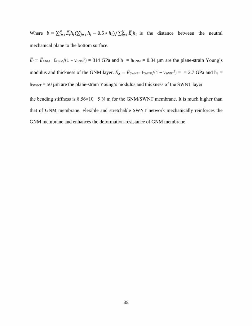
The bending stiffness of GNM can be calculated as
�̅�𝐼𝐺𝑁𝑀 = �̅�𝐺𝑁𝑀ℎ𝐺𝑁𝑀3/12
�̅�GNM= EGNM/(1 − νGNM2) is the plane-strain Young's modulus and the poisson’s ratio is 0.16. The
thickness of the GNM membrane is hGNM = 0.34 µm.
The bending stiffness of the bi-layer GNM/SWNT layer (�̅�IGNM/SWNT) can be calculated as [54]
�̅�IGNM/SWNT = ∑ 𝐸�̅�ℎ𝑖[(𝑏 − ∑ ℎ𝑗)2 + (𝑏 + ∑ ℎ𝑗) + 1/3 ∗ ℎ𝑖
2𝑖𝑗=1
𝑖𝑗=1 )𝑁
𝑖=1
38
Where 𝑏 = ∑ 𝐸�̅�ℎ𝑖(∑ ℎ𝑗 − 0.5 ∗ ℎ𝑖𝑖𝑗=1 )/∑ 𝐸�̅�ℎ𝑖
𝑁𝑖=1
𝑁𝑖=1 is the distance between the neutral
mechanical plane to the bottom surface.
�̅�1= �̅�GNM= EGNM/(1 − νGNM2) = 814 GPa and h1 = hGNM = 0.34 µm are the plane-strain Young’s
modulus and thickness of the GNM layer. 𝐸2̅̅ ̅ = �̅�SWNT= ESWNT/(1 – νSWNT2) = = 2.7 GPa and h2 =
hSWNT = 50 µm are the plane-strain Young’s modulus and thickness of the SWNT layer.
the bending stiffness is 8.56×10− 5 N·m for the GNM/SWNT membrane. It is much higher than
that of GNM membrane. Flexible and stretchable SWNT network mechanically reinforces the
GNM membrane and enhances the deformation-resistance of GNM membrane.

39
Chapter 5 Conclusion
In this thesis, a heterogeneous flexible and transient PVA/Zn electronics are fabricated by photonic
sintering. Three applications, ECG sensor, EMG sensor and temperature sensor are applied by this
PVA/Zn functional assembly. Some parameters, like the thickness of PVA membrane, size of Zn
electrodes need further studies. The encapsulation layer can be added later to prevent oxidation of
metal layer after photonic sintering. Another simulation about heterogenous assembly,
GNM/SWNT membrane is calculated under uniaxial stretching condition. This simulation focus
on the equivalent modeling of porous multilayer structure at nanoscale. The Young’s modulus of
bilayer structure should between the range from 7.95 GPa to 12.08 GPa which is consistent with
experimental data [52].

40
References
[1] Q. Cao et al., "Medium-scale carbon nanotube thin-film integrated circuits on flexible plastic
substrates," vol. 454, no. 7203, p. 495, 2008. [2] G. H. Gelinck et al., "Flexible active-matrix displays and shift registers based on solution-
processed organic transistors," vol. 3, no. 2, p. 106, 2004. [3] D. J. Lipomi, B. C. K. Tee, M. Vosgueritchian, and Z. J. A. M. Bao, "Stretchable organic solar cells,"
vol. 23, no. 15, pp. 1771-1775, 2011. [4] D.-H. Kim et al., "Dissolvable films of silk fibroin for ultrathin conformal bio-integrated
electronics," vol. 9, no. 6, p. 511, 2010. [5] Y. Liu, M. Pharr, and G. A. J. A. n. Salvatore, "Lab-on-skin: a review of flexible and stretchable
electronics for wearable health monitoring," vol. 11, no. 10, pp. 9614-9635, 2017. [6] J. W. Jeong et al., "Capacitive epidermal electronics for electrically safe, long‐term
electrophysiological measurements," vol. 3, no. 5, pp. 642-648, 2014. [7] S. Xu et al., "Soft microfluidic assemblies of sensors, circuits, and radios for the skin," vol. 344,
no. 6179, pp. 70-74, 2014. [8] D.-H. Kim et al., "Epidermal electronics," vol. 333, no. 6044, pp. 838-843, 2011. [9] R. C. Webb et al., "Ultrathin conformal devices for precise and continuous thermal
characterization of human skin," vol. 12, no. 10, p. 938, 2013. [10] J. W. Lee et al., "Soft, thin skin-mounted power management systems and their use in wireless
thermography," vol. 113, no. 22, pp. 6131-6136, 2016. [11] W. Gao et al., "Fully integrated wearable sensor arrays for multiplexed in situ perspiration
analysis," vol. 529, no. 7587, p. 509, 2016. [12] A. Koh et al., "A soft, wearable microfluidic device for the capture, storage, and colorimetric
sensing of sweat," vol. 8, no. 366, pp. 366ra165-366ra165, 2016. [13] B. Xu et al., "An epidermal stimulation and sensing platform for sensorimotor prosthetic control,
management of lower back exertion, and electrical muscle activation," vol. 28, no. 22, pp. 4462-4471, 2016.
[14] X. Huang et al., "Materials and designs for wireless epidermal sensors of hydration and strain," vol. 24, no. 25, pp. 3846-3854, 2014.
[15] S. C. Mannsfeld et al., "Highly sensitive flexible pressure sensors with microstructured rubber dielectric layers," vol. 9, no. 10, p. 859, 2010.
[16] C. Dagdeviren et al., "Conformable amplified lead zirconate titanate sensors with enhanced piezoelectric response for cutaneous pressure monitoring," vol. 5, p. 4496, 2014.
[17] S. W. Hwang et al., "25th anniversary article: materials for high‐performance biodegradable
semiconductor devices," vol. 26, no. 13, pp. 1992-2000, 2014. [18] K. K. Fu, Z. Wang, J. Dai, M. Carter, and L. J. C. o. M. Hu, "Transient electronics: materials and
devices," vol. 28, no. 11, pp. 3527-3539, 2016. [19] H. J. J. o. M. R. Cheng, "Inorganic dissolvable electronics: Materials and devices for biomedicine
and environment," vol. 31, no. 17, pp. 2549-2570, 2016. [20] H. Cheng, V. J. T. Vepachedu, and A. M. Letters, "Recent development of transient electronics,"
vol. 6, no. 1, pp. 21-31, 2016. [21] S.-K. Kang et al., "Bioresorbable silicon electronic sensors for the brain," vol. 530, no. 7588, p.
71, 2016.

41
[22] K. J. Yu et al., "Bioresorbable silicon electronics for transient spatiotemporal mapping of electrical activity from the cerebral cortex," vol. 15, no. 7, p. 782, 2016.
[23] L. Yin et al., "Dissolvable metals for transient electronics," vol. 24, no. 5, pp. 645-658, 2014. [24] P. P. Mueller et al., "Histological and molecular evaluation of iron as degradable medical implant
material in a murine animal model," vol. 100, no. 11, pp. 2881-2889, 2012. [25] H. Hermawan, A. Purnama, D. Dube, J. Couet, and D. J. A. b. Mantovani, "Fe–Mn alloys for
metallic biodegradable stents: degradation and cell viability studies," vol. 6, no. 5, pp. 1852-1860, 2010.
[26] F. J. A. b. Witte, "The history of biodegradable magnesium implants: a review," vol. 6, no. 5, pp. 1680-1692, 2010.
[27] N. Kirkland, N. Birbilis, and M. J. A. b. Staiger, "Assessing the corrosion of biodegradable magnesium implants: a critical review of current methodologies and their limitations," vol. 8, no. 3, pp. 925-936, 2012.
[28] M.-C. Zhao, P. Schmutz, S. Brunner, M. Liu, G.-l. Song, and A. J. C. S. Atrens, "An exploratory study of the corrosion of Mg alloys during interrupted salt spray testing," vol. 51, no. 6, pp. 1277-1292, 2009.
[29] E. Patrick, M. E. Orazem, J. C. Sanchez, and T. J. J. o. n. m. Nishida, "Corrosion of tungsten microelectrodes used in neural recording applications," vol. 198, no. 2, pp. 158-171, 2011.
[30] W. Badawy and F. J. E. A. Al-Kharafi, "Corrosion and passivation behaviors of molybdenum in aqueous solutions of different pH," vol. 44, no. 4, pp. 693-702, 1998.
[31] P. K. Bowen, J. Drelich, and J. J. A. m. Goldman, "Zinc exhibits ideal physiological corrosion behavior for bioabsorbable stents," vol. 25, no. 18, pp. 2577-2582, 2013.
[32] M. S. B. Husain, A. Gupta, B. Y. Alashwal, S. J. E. S. Sharma, Part A: Recovery, Utilization,, and E. Effects, "Synthesis of PVA/PVP based hydrogel for biomedical applications: a review," vol. 40, no. 20, pp. 2388-2393, 2018.
[33] F. Parvin, M. Rahman, J. M. Islam, M. A. Khan, and A. Saadat, "Preparation and characterization of starch/PVA blend for biodegradable packaging material," in Advanced Materials Research, 2010, vol. 123, pp. 351-354: Trans Tech Publ.
[34] S.-W. Hwang et al., "Dissolution chemistry and biocompatibility of single-crystalline silicon nanomembranes and associated materials for transient electronics," vol. 8, no. 6, pp. 5843-5851, 2014.
[35] Y. Galagan et al., "Photonic sintering of inkjet printed current collecting grids for organic solar cell applications," vol. 14, no. 1, pp. 38-46, 2013.
[36] Y. Yamamoto et al., "Efficient Skin Temperature Sensor and Stable Gel‐Less Sticky ECG Sensor
for a Wearable Flexible Healthcare Patch," vol. 6, no. 17, p. 1700495, 2017. [37] B. K. Mahajan et al., "Aerosol printing and photonic sintering of bioresorbable zinc nanoparticle
ink for transient electronics manufacturing," vol. 61, no. 6, p. 060412, 2018. [38] M. Khalil, S. Saeed, Z. J. J. o. M. S. P. A. P. Ahmad, and A. Chemistry, "Properties of binary
polyimide blends containing hexafluoroisopropylidene group," vol. 44, no. 1, pp. 55-63, 2007. [39] A. Houghton and D. Gray, Making sense of the ECG: a hands-on guide. CRC Press, 2008. [40] C. Lou et al., "Flexible graphene electrodes for prolonged dynamic ECG monitoring," vol. 16, no.
11, p. 1833, 2016. [41] Y. Yu, J. Zhang, and J. J. P. O. Liu, "Biomedical implementation of liquid metal ink as drawable
ECG electrode and skin circuit," vol. 8, no. 3, p. e58771, 2013. [42] D. Yamamoto, S. Nakata, K. Kanao, T. Arie, S. Akita, and K. Takei, "All-printed, planar-type multi-
functional wearable flexible patch integrated with acceleration, temperature, and ECG sensors," in 2017 IEEE 30th International Conference on Micro Electro Mechanical Systems (MEMS), 2017, pp. 239-242: IEEE.

42
[43] W. Pei et al., "Skin-potential variation insensitive dry electrodes for ECG recording," vol. 64, no. 2, pp. 463-470, 2016.
[44] A. Miyamoto et al., "Inflammation-free, gas-permeable, lightweight, stretchable on-skin electronics with nanomeshes," vol. 12, no. 9, p. 907, 2017.
[45] B. Sun et al., "Gas‐Permeable, Multifunctional On‐Skin Electronics Based on Laser‐Induced
Porous Graphene and Sugar‐Templated Elastomer Sponges," vol. 30, no. 50, p. 1804327, 2018.
[46] M. C. Garcia and T. J. R. a. d. m. d. d. Vieira, "Surface electromyography: Why, when and how to use it," vol. 4, no. 1, pp. 17-28, 2011.
[47] D. Pollock, Thermocouples: theory and properties. Routledge, 2017. [48] N. Yi et al., "Fully Water-Soluble, High-Performance Transient Sensors on a Versatile
Galactomannan Substrate Derived from the Endosperm," vol. 10, no. 43, pp. 36664-36674, 2018.
[49] S. Z. Cheng, Handbook of thermal analysis and calorimetry: applications to polymers and plastics. Elsevier, 2002.
[50] P. Xiao et al., "2D Janus Hybrid Materials of Polymer‐Grafted Carbon Nanotube/Graphene Oxide
Thin Film as Flexible, Miniature Electric Carpet," vol. 25, no. 16, pp. 2428-2435, 2015. [51] F. Tristán-López et al., "Large area films of alternating graphene–carbon nanotube layers
processed in water," vol. 7, no. 12, pp. 10788-10798, 2013. [52] Y. B. Yang et al., "Large-area graphene-nanomesh/carbon-nanotube hybrid membranes for ionic
and molecular nanofiltration," (in English), Science, vol. 364, no. 6445, pp. 1057-+, Jun 14 2019. [53] M. Isida, H. J. I. j. o. s. Igawa, and structures, "Analysis of a zig-zag array of circular holes in an
infinite solid under uniaxial tension," vol. 27, no. 7, pp. 849-864, 1991. [54] S. Wang et al., "Mechanics of epidermal electronics," vol. 79, no. 3, 2012.