Embed Size (px)
Citation preview
Exciton Dynamics in CdS-Ag2S Nanorods with Tunable Composition Probed by UltrafastTransient Absorption Spectroscopy
Paul Peng,† Bryce Sadtler,†,‡ A. Paul Alivisatos,†,‡ and Richard J. Saykally*,†,§
Department of Chemistry, UniVersity of California, Berkeley, California 94720, Materials Sciences DiVision,Lawrence Berkeley National Laboratory, California 94720, and Chemical Sciences DiVision, LawrenceBerkeley National Laboratory, California 94720
ReceiVed: December 9, 2009; ReVised Manuscript ReceiVed: February 11, 2010
Electron relaxation dynamics in CdS-Ag2S nanorods have been measured as a function of the relative fractionof the two semiconductors, which can be tuned via cation exchange between Cd2+ and Ag+. The transientbleach of the first excitonic state of the CdS nanorods is characterized by a biexponential decay correspondingto fast relaxation of the excited electrons into trap states. This signal completely disappears when the nanorodsare converted to Ag2S but is fully recovered after a second exchange to convert them back to CdS, demonstratingannealing of the nonradiative trap centers probed and the robustness of the cation exchange reaction. Partialcation exchange produces heterostructures with embedded regions of Ag2S within the CdS nanorods. Transientbleaching of the CdS first excitonic state shows that increasing the fraction of Ag2S produces a greatercontribution from the fast component of the biexponential bleach recovery, indicating that new midgaprelaxation pathways are created by the Ag2S material. Transient absorption with a mid-infrared probe furtherconfirms the presence of states that preferentially trap electrons on a time scale of 1 ps, 2 orders of magnitudefaster than that of the parent CdS nanorods. These results suggest that the Ag2S regions within the heterostuctureprovide an efficient relaxation pathway for excited electrons in the CdS conduction band.
I. Introduction
The size, shape, and chemical composition of semiconductornanocrystals control their resulting optoelectronic properties. Forinstance, in both semiconductor alloys and heterostructures, theband gap absorption and emission energies can be widely tunedthrough the spatial variation of composition.1-8 The compositionof colloidal nanocrystals is typically mediated by the time-dependent variation of cation and anion precursor concentrationsduring solution-phase nucleation and growth.1,2 Alternatively,nanocrystals of a desired shape and size can be chemicallytransformed, postsynthesis, through a solid-state reaction intoa new composition. Notably, in ionic nanocrystals, cationexchange can be used to partially or fully replace the cationswithin the lattice of the crystal with substitutional cations fromsolution.6-12 Such solid-state reactions can occur with remark-able efficiency, owing to molecular-like reaction kinetics ofnanoscale materials possessing high surface-to-volume ratios.8-10,13
Furthermore, when the exchange is limited to occur throughonly a portion of the nanocrystal, heterostructures are producedcontaining distinct regions of the secondary and host crystalsconnected by a continuous anion framework.
Several recent reports have characterized the structural andstatic optical properties of semiconductor nanocrystals producedby cation exchange.7-11 Transmission electron microscopy(TEM) and X-ray diffraction (XRD) show that the crystals retaintheir size and shape and are highly crystalline after the exchangereaction. However, such techniques are rather insensitive to localdefects that may be introduced, and so far, there has not been
a systematic determination of how such chemical transforma-tions affect exciton dynamics in the nanocrystals. There isevidence from related systems that the structural disorder (suchas vacancies or substitutional impurities) introduced by theinterdiffusion of ions can lead to additional relaxation pathwaysfor photoexcited charge carriers.14,15
We report pump-probe measurements in CdS-Ag2S nano-rods to characterize the effect that cation exchange has on therelaxation of excited carriers. We have chosen this materialsystem as the relative fraction of the two semiconductors canbe readily controlled by the amount of Ag+ that is added to theCdS nanorods (or conversely the amount of Cd2+ added to Ag2Snanorods).8,16 Moreover, the combination of semiconductors thatpossess a type I (sandwiched) electronic band alignment canlead to the transfer of excited electrons and holes in the wideband gap material (CdS) to the smaller band gap material(Ag2S), provided that competing relaxation pathways areinhibited.8 We study carrier relaxation dynamics by monitoringthe transient bleaching of the first excitonic transition (1Se), andthe intraband absorption (1Se-1Pe) of electrons in the conduc-tion band of CdS nanorods. The change in time constants ofthe relaxation dynamics following complete and cyclic conver-sion between CdS and Ag2S nanorods (i.e., forward conversionfrom CdS to Ag2S and back conversion to CdS) is used tocharacterize how the process of cation exchange can lead tonew relaxation pathways through introduction of defect states.Partial cation exchange to make CdS-Ag2S heterostructuresdemonstrates how the presence of Ag2S affects the relaxationof excited carriers in the CdS material.
II. Experimental Methods
A. CdS Synthesis. Colloidal CdS nanorods were synthesizedaccording to previously published procedures.8,10 A detaileddescription of the reaction conditions is provided in the
* To whom correspondence should be addressed. E-mail: [email protected].
† University of California, Berkeley.‡ Materials Sciences Division, Lawrence Berkeley National Laboratory.§ Chemical Sciences Division, Lawrence Berkeley National Laboratory.
J. Phys. Chem. C 2010, 114, 5879–5885 5879
10.1021/jp9116722 2010 American Chemical SocietyPublished on Web 03/04/2010

Supporting Information. Briefly, cadmium oxide was complexedwith propyl- and octadecyl-phosphonic acids in the coordinatingsolvent, trioctylphosphine oxide, at high temperature under anargon atmosphere to form cadmium-phosphonate. Trioctylphos-phine (TOP) and trioctylphosphine sulfide (TOPS) were injectedat 320 °C to induce nucleation of the CdS nanorods, which weregrown at high temperature for approximately 70 min, duringwhich time additional TOP and TOPS were added slowly via asyringe pump. After cooling the reaction, the nanorods werethen washed several times with organic solvents and surfactantsto remove the remaining Cd-phosphonate complex. The CdSnanorods were dispersed in toluene and stored in an argon-filledglovebox. While a variety of coordinating molecules are usedin the synthesis and subsequent cleaning of the nanorods,previous studies indicate that cadmium chalcogenide nanocryst-als grown by such methods are primarily passivated by thealkylphosphonic acids used to control their growth kinetics.17
B. Cation Exchange. Ag+ cation exchange was used toconvert CdS nanorods into CdS-Ag2S nanorod heterostructuresand Ag2S nanorods, using slight modifications to our previousreports.8 The reactions were performed inside an argon-filledglovebox at room temperature. The extent of conversion canbe controlled by the amount of Ag+ added to a knownconcentration of CdS nanorods. For Ag+/Cd2+ ratios of 0.50,1.0, and 1.5, the volume fractions of Ag2S within the nanorodswere 0.12, 0.19, and 0.30 as measured from TEM images.Excess Ag+ was used for full exchange (Ag+/Cd2+ > 4). Themolar concentration of Cd2+ ions for each CdS nanorod solutionwas determined by inductively coupled plasma atomic emissionspectroscopy of acid-digested samples. Typical molar extinctioncoefficients used to obtain the Cd2+ concentration in the CdSnanorod solutions were 3000 L mol-1 cm-1 at 300 nm measuredby visible absorption spectroscopy. The amount of Cd2+ in theCdS nanorod solution for each reaction was between 1 × 10⁻⁶
and 3 × 10⁻⁶ mol. In a typical reaction, 8 mg of silver nitrate(AgNO3) was dissolved in 3 mL of methanol (MeOH) and wasthen diluted further with MeOH depending on the desired Ag+/Cd2+ ratio. The AgNO3 solution (∼0.5-1 mL) was added to alarger amount of toluene (∼1-3 mL) so that the nanorods wouldremain soluble during the reaction. A solution of CdS nanorodsin toluene (∼0.15-0.6 mL) was then added to the Ag+ solutionwhile stirring. The color of the nanocrystal solution changesrapidly (<1 s) from yellow to dark brown after mixing of theAg+ and CdS solutions. The converted nanorods were subse-quently washed by the addition of MeOH followed by centrifu-gation and removal of the supernatant. To convert the Ag2Snanorods back to CdS, a solution of the Ag2S nanorods wasredispersed in tetrahydrofuran and mixed with a large excessof cadmium nitrate (Cd2+/Ag+ ∼ 100) dissolved in acetonitrile(MeCN). A drop of tributylphosphine (TBP) was then addedand the reaction was heated to approximately 85 °C for 20 minwhile stirring. The Supporting Information provides furthersynthetic detail for each of the samples used in these studies.
C. Nanocrystal Characterization. Bright field TEM imageswere obtained using an FEI Tecnai G2 Supertwin electronmicroscope operating at 200 kV. TEM samples were preparedby placing a drop of the nanocrystal solution onto a carbon-coated copper grid in ambient atmosphere. Size statistics forthe length and diameter of the CdS nanorods before and aftercation exchange were determined from TEM images taken at amagnification of 97000× to 195000× using Image-Pro Plus orImageJ software and making at least 250 measurements. Thevolume fractions of Ag2S within the CdS nanorods for differentAg+/Cd2+ ratios were calculated by measuring the size of the
Ag2S regions within 100 nanorods for each sample andestimating their volume from the two-dimensional image. SmallAg2S regions were approximated as spheres, whereas Ag2Sregions that spanned the diameter of the nanorods wereapproximated as cylinders.
For absorption and fluorescence measurements, the nano-crystals were precipitated and redispersed in tetrachloroethylene,and placed in a 1 cm path length FUV quartz cuvette with aflat absorption profile from ∼170 to 2200 nm. Absorptionspectra were recorded on an Agilent 8453 UV-visible spec-trophotometer. Fluorescence spectra were recorded on a HoribaJobin Yvon Fluorolog 3 equipped with a Triax 320 spectrometer.The excitation wavelength was 400 nm, and a photomultipliertube was used for detection. The emission spectra were correctedfor the wavelength-dependent response of the emission gratingand detector and the background of the solvent.
Fluorescence quantum yields were measured by comparingthe integrated emission intensity of the nanocrystal sample withthat of a reference dye. Coumarin 480 (Exciton Inc.) was used,which has a quantum yield of 74% in ethanol at an excitationwavelength of 390 nm.18 The optical densities of the solutionswere matched at the excitation wavelength and were ap-proximately 0.02 at 390 nm for both the CdS nanorods and theCoumarin 480 dye. The quantum yields were corrected for therefractive index of the solvent and small differences in opticaldensity of the solution.
D. Femtosecond Transient Spectroscopy. A 1 kHz regen-eratively amplified titanium:sapphire laser (τ ) 150 fs, λcenter
) 800 nm) was used for the time-resolved experiments. Themajority (90%) of this output pumps a commercial (LightConversion, TOPAS) optical parametric amplifier or a home-built noncollinear optical parametric amplifier to tune the probefrom the visible to the mid-infrared. A normalized transientbleach spectrum obtained with a white light continuum probedetermined the lowest excitonic transition for the CdS nanorodsto be at an energy corresponding to a probe wavelength of λ )470 nm. Difference frequency generation between the opticalparametric amplifier signal and idler photons in a AgGaS2
nonlinear crystal produced the mid-infrared (λ ) 4 µm) probefor intraband absorption experiments, as determined by theenergy difference between the 1Se and 1Pe levels. The remaining(10%) fundamental output is frequency-doubled (λ ) 400 nm)and used as the optical pump (4 mW, 200 µm spot size) in theexperiments. The pump beam path traverses an optical delayline and is also optically chopped at 500 Hz for gated boxcarintegrator detection. Either a photodiode or mercury cadmiumtelluride detector is used to measure the differential probetransmission ∆T/T as a function of optical delay. A neutraldensity filter maintained a pump fluence such that, on average,there was less than one electron-hole pair that was excited pernanocrystal, ⟨Ne-h⟩ ) 0.30 ( 0.08, given a 0.8-1.4 range inoptical densities and extinction coefficient of 9.3 × 106 cm-1
M-1. The nanocrystals were dissolved in toluene and placed ina 1 mm path length NIR cuvette. Between three and fiveaveraged transients represent each of the dynamics traces shownherein, and all experiments were conducted at room temperature.
III. Results and Discussion
A. Transient Bleaching and Absorption Dynamics. Asshown in Figure 1, electrons and holes photogenerated abovethe band gap (so-called hot carriers) in semiconductor nano-crystals typically have the following relaxation scheme: First,intraband relaxation (Figure 1B) of the carriers to the band edgeoccurs, which can be fast (e1 ps) depending on the overlap
5880 J. Phys. Chem. C, Vol. 114, No. 13, 2010 Peng et al.

between electron and hole wave functions. Good overlap as aconsequence of spatial confinement can lead to a transfer ofexcess energy from the electron to the hole and fast intrabandrelaxation.19 Second, carriers may be trapped (Figure 1C) byintrinsic surface states such as dangling bonds due to incompletepassivation of the nanocrystal surface, which is also a relativelyfast process (0.1-1 ps).20 As the Lewis basic surfactants(alkylphosphonates) used to grow and passivate the CdSnanocrystals bind much stronger to electron deficient Cd2+ overS2-, the surface is believed to be Cd2+ rich.17 Cd2+ ions thatare not fully passivated by the alkylphosphonate ligands canlead to shallow electron traps, while S2- ions at the nanocrystalsurface act as sites for hole trapping.21 Both electron and holetrapping have been observed in II-VI semiconductor nano-crystals, although their contribution to the relaxation dynamicscan vary with the chemical composition of the nanocrystal, theligands used to passivate their surface, as well as the solvent inwhich the nanocrystals are dispersed.14,20,22 The degree ofpassivation will determine whether carriers preferentially re-combine radiatively at the band edge or radiatively/nonradia-tively through the trap states.
One method to characterize the relaxation of hot carriers isby monitoring the occupation of an energy level as a functionof time. After photogeneration of an electron and intrabandrelaxation, the first excitonic transition 1Se level becomespartially saturated and the transition bleaches for probe photonsarriving at later times (Figure 1B). Transient bleaching experi-ments determine both the time it takes for the bleach to reachits maximum (i.e., the rise time, τrise, of carriers cooling to thatlevel) and the ground state recovery time, τrec, which comprisesall processes that return the system to its original state beforeexcitation. Alternatively, a probe photon with an energycorresponding to the difference between the 1Se and 1Pe levelscan be used to monitor the intraband transition of an electronin the conduction band to obtain dynamical information aboutthe excited state time evolution.23
Transient bleaching and absorption dynamics of the parentCdS nanorods used in the experiments are shown in Figure 2.The rise time of the bleach is τrise ) 1.7 ( 0.1 ps and therecovery of the bleach is best fit with a biexponential decayfunction yielding time constants of τ1 ) 202 ( 52 ps and τ2 )3300 ( 770 ps. Physically speaking, the faster decay timecomponent (τ1 ) 1-100 ps) corresponds to a convolution oftrapping processes while the slower (τ2 ) 100-1000 ps) timecomponent represents long-lived states. The latter pathway could
be any one of the situations involving separated charges on thenanocrystal, radiative trap recombination, trap-to-trap hopping,or relaxation through a series of nonradiative levels.24 There isevidence that low-energy trap states (from a distribution of trapstates) play an especially dominant role in the longer lifetimes.22
Also plotted in Figure 2 is the intraband absorption from the1Se-1Pe transition, where a monoexponential fitted decayconstant of τdecay ) 286 ( 81 ps describes the electron’s lifetimein the 1Se level. The noticeably higher noise in the intrabandsignal is due to greater pulse-to-pulse fluctuations in thenonlinear optically generated mid-infrared probe. The value ofτdecay is comparable to that of τ1 in the transient bleaching trace,demonstrating the correlation between the two techniques.
B. Sequential Conversion between CdS and Ag2S Nano-rods. TEM images of CdS and Ag2S nanorods are shown inFigure 3. A molar excess of Ag+ added to the nanorods (Ag+/Cd2+ > 2 as two Ag+ ions are need to replace one Cd2+ ion)completely converts the composition to Ag2S, while closelypreserving the dimensions of the original nanorods (Figure 3Band Figure S1 in the Supporting Information). There is anincrease in the average nanorod diameter from 5.3 ( 0.4(average ( first standard deviation) to 5.7 ( 0.5 nm and adecrease in the average nanorod length from 66 ( 14 to 58 (14 nm following exchange. The small change in dimensions isin part due to the difference in lattice volumes of the twocrystals. Disruption of the anion framework during cationexchange can also cause partial restructuring of the nanocrystaltoward a less anisotropic shape (i.e., lower surface area).9 Somenanorods are also observed to coalesce during the transforma-tion. To convert the Ag2S nanocrystals back to CdS, a largeexcess of Cd2+ ions, higher temperature, and coordinatingmolecules with greater binding strengths to Ag+ (i.e., MeCNand TBP) are used.9,12,26 The reverse exchange reaction also
Figure 1. Energy level schemes of parent CdS nanorods andsubsequent relaxation pathways: (A) An electron-hole pair is createdby the pump pulse (λpump ) 400 nm); intrinsic shallow and deep trapstates are present within the band gap. (B) Rapid intraband relaxationof electron and hole to the band edge follows, and the occupation ofthe 1Se level can be probed either by transient bleaching (λprobe ) 470nm) or intraband absorption (λprobe ) 4 µm). If band edge radiativerecombination does not occur, then (C) further trapping of the holeinto shallow/deep traps can lead to trap relaxation.
Figure 2. Transient bleaching (-9-) and intraband absorptiondynamics (-) of parent CdS nanorods used in the experiments. Thedecay of the bleach is >4 ns and represents the ground state recoveryof the system. In contrast, the decay of the intraband absorption signifiesthe lifetime of the electron in the 1Se level and is therefore acomplementary probe of the excited state dynamics.
Figure 3. TEM images of CdS and Ag2S nanorods: (A) the initialCdS nanorods; (B) Ag2S nanorods made by full conversion of the CdSnanorods; (C) recovered CdS′ nanorods after back conversion fromAg2S. The dark regions of the nanorods in part B are formed by partialreduction of Ag2S under irradiation of the electron beam.25
Exciton Dynamics in CdS-Ag2S Nanorods J. Phys. Chem. C, Vol. 114, No. 13, 2010 5881

generally preserves the nanorod morphology, where the dimen-sions of the recovered CdS nanorods are 5.0 ( 0.5 nm indiameter and 60 ( 14 nm in length. However, after thesequential exchange reactions, there is a larger variation in thediameter along individual nanorods.
Absorption and fluorescence spectra following the sequentialexchange reactions (CdSf Ag2Sf CdS′) are shown in Figure4. The absorption spectrum of the initial CdS nanorods displayswell-defined excitonic features with the first exciton peak at∼471 nm (2.6 eV), whereas the bulk band gap, Eg, of CdS is2.5 eV (λ ) 497 nm).27 Absorption from the fully convertedAg2S nanocrystals is broad, with no clear excitonic features, asAg2S nanocrystals generally do not exhibit quantum confinementeffects and possess a band gap similar to that of bulk Ag2S (Eg
∼ 1.0 eV, λ ∼ 1240 nm).28,29 However, the back conversion ofthe Ag2S nanorods to CdS is accompanied by recovery of theoriginal exciton features, with the spectral position of the firstexciton peak located within 2 nm of the original CdS nanorods.
CdS nanorods exhibit both excitonic emission as well broademission to the red of the exciton peak arising from defect states.Exciton emission occurs at 488 nm, while the broad peakcentered at ∼700 nm has previously been attributed to excessCd2+ (i.e., S2- vacancies) at the surface of the nanocrystal.21
The Ag2S nanorods show no emission in the visible region,although weak near-infrared emission corresponding to Eg forAg2S has been previously reported.8 The fluorescence spectrumof the back-converted CdS nanorods displays greatly increasedtrap emission with only very weak band edge emission (Figure4B). The quantum yields (QYs) of the exciton and trap emission
in the initial CdS sample are approximately 0.1 and 5%,respectively, while the trap emission QY in the recovered CdSnanorods is approximately 30%. As the reverse exchange isperformed with a large excess of Cd2+, surface adsorption ofthese cations during exchange is expected to increase the numberof electron trap states.21 While residual Ag+ ions within the CdSlattice or at its surface may also act as trap states, the amountof Ag+ is expected to be low on the basis of the absorptionspectra of the recovered nanorods and the bleaching dynamicsdescribed below.
Figure 5 shows transient bleaching dynamics of the initialCdS nanorods and the recovered ones after conversion to Ag2S.The transients of the initial and recovered CdS nanorods arenearly identical at short times (delay of 0-12 ps). Biexponentialfits to the decay dynamics are τ1 ) 350 ( 100 ps and τ2 )3200 ( 200 ps for the initial CdS nanorods and τ1 ) 100 ( 32ps and τ2 ) 3470 ( 277 ps for the back-converted ones. Thetime constant, τ1, is shorter in the recovered sample comparedto the original CdS nanorods, indicating that new trap stateshave been introduced. The near complete recovery of theoriginal exciton features upon back exchange dynamicssuggests there is little reorganization of the anion sublattice,except near the surface of the nanocrystal, in agreement withthe increase in surface trap emission after double exchange.This is quite remarkable considering the different latticevolumes of CdS and Ag2S (∼15%) as well as their differentsymmetries (hexagonal versus monoclinic). Thus, cationexchange is able to completely and reversibly alter the excitondynamics of semiconductor nanocrystals, where the maineffect is from the change in chemical composition, althoughsome surface states were introduced through the process.
Figure 4. Absorbance and fluorescence spectra of CdS and Ag2Snanorods: (A) absorbance spectra of CdS nanorods, converted Ag2Snanorods, and back-exchanged CdS′ nanorods; (B) fluorescence spectraof the same samples showing the large increase in surface trap emissionafter sequential exchange. The inset shows the band edge emission fromthe CdS samples on a 10× scale. The colors of the plots match theborders of the TEM images in Figure 3 for the same samples.
Figure 5. (A) Comparison of the transient bleach dynamics of CdSnanorods (s, gray) to the nanorods that underwent full conversion toAg2S followed by back exchange to CdS (-[-, black). (B) Magnifica-tion of the dynamics at early time delays indicates that electronrelaxation follows a similar pathway after forward and back exchange.The Ag2S nanorods show no signal in these measurements.
5882 J. Phys. Chem. C, Vol. 114, No. 13, 2010 Peng et al.

C. Exciton Dynamics of CdS-Ag2S Nanorod Hetero-structures. After evaluating how the cation exchange reactionaffects carrier dynamics through the introduction of surfacestates (see previous section), we can now look at the dynamicsof CdS-Ag2S heterostructures made with varying Ag+/Cd2+
ratios to control the relative volume fraction of Ag2S withinthe nanorods. TEM images of the heterostructures are shownin Figure 6, where the regions of Ag2S formed within the CdSnanorods appear as darker spots, as the Ag2S lattice has a greateratomic density. The volume fraction of Ag2S within the nanorodsgrows larger as the Ag+/Cd2+ ratio used in the exchangereactions is increased.8 The approximate volume fractions ofAg2S within the nanorods are 0.12, 0.19, and 0.30 as measuredfrom the TEM images. Absorbance and fluorescence spectrafor the CdS-Ag2S nanorods are shown in Figure 7. Forincreasing amounts of Ag+ added, an absorption tail to the redof the CdS band edge grows stronger in intensity due to thepresence of the smaller band gap Ag2S material (Figure 7A).
However, the spectral position of the first CdS exciton featureat 470 nm remains the same, indicating that there is little changein the average nanorod diameter during the reaction.30 Thefluorescence spectra show that, even for low fractions ofexchange, exciton emission from the CdS material is quenched.Surface trap emission from CdS is still present in the hetero-structures but becomes weaker in intensity as the Ag2S regionsgrow in size. Because the Ag2S material forms near the surfaceof the CdS nanorod for low fractions of exchange, its presencemay partially remove radiative surface traps. The absence ofband edge emission and decrease in trap emission suggest thatnew relaxation processes are made available by the presenceof Ag2S within the nanorods which occur on a much faster timescale than radiative recombination.
Intraband absorption (1Se-1Pe) dynamics of CdS nanorodssubject to varying degrees of cation exchange all yield a similartrace shown in Figure 8. That is, the intraband decay constants(τdecay ) 7-22 ps) of the CdS-Ag2S heterostructures aresignificantly faster than that of the parent CdS nanorods. Wecan gain a clearer understanding of the pathways with transientbleaching data shown in Figure 9. Not only is the electronleaving the 1Se state faster (as shown by the intrabanddynamics), but it is also recovering the ground state morequickly as the fast component of the bleach decay, τ1, decreasesby 2 orders of magnitude ()1.1-1.4 ps) in the heterostrucutures
Figure 6. TEM images of CdS-Ag2S heterostructures made withincreasing Ag+/Cd2+ ratios and with approximate Ag2S/CdS volumefractions of (A) 0.12, (B) 0.19, and (C) 0.30.
Figure 7. Absorbance and fluorescence spectra of CdS-Ag2S nanorodheterostructures. (A) Absorbance spectra for increasing volume fractionsof Ag2S. The Ag2S/CdS ratio is given above each plot. (B) Fluorescencespectra of the same samples showing quenching of both the CdS excitonand trap emission as the Ag2S fraction increases. The colors of theplots match the borders of the TEM images in Figure 6 for the samesamples.
Figure 8. Intraband absorption dynamics of CdS nanorods (-2-)compared to a representative trace (-) of cation-exchanged nanorods.All of the cation-exchanged samples exhibit significantly faster decaythan that of the initial CdS nanorods, which suggests that electronrelaxation pathways are created in the Ag2S regions.
Figure 9. Normalized and offset transient bleaching traces of the 1Se
transition as a function of Ag2S fraction: Ag2S /CdS ) 0.0 (-[-),Ag2S/CdS ) 0.12 (-9-), Ag2S/CdS ) 0.19 (-2-), and Ag2S /CdS) 0.30 (-×-). As the fraction of Ag2S increases in the nanorods, thecontribution from the fast time component τ1 of the transient bleachrecovery also increases until it dominates the dynamics at 0.30exchange. Higher exchange fractions show little signal due to the smallamount of CdS they contain.
Exciton Dynamics in CdS-Ag2S Nanorods J. Phys. Chem. C, Vol. 114, No. 13, 2010 5883
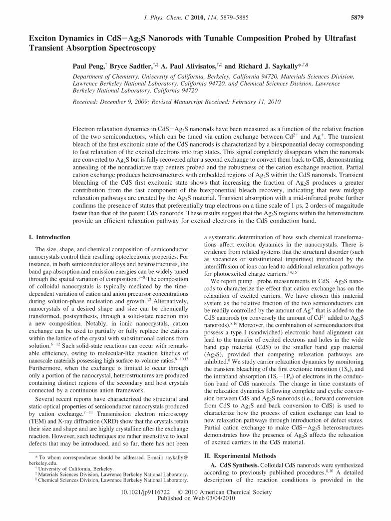
compared to the initial CdS nanorods. Biexponential fits to thebleaching decay curves show that the weighting of τ1 increasesas the volume fraction of Ag2S increases (Figure 10). The long-lived states present in the original CdS nanorods are no longerthe dominant relaxation pathways; instead, fast trapping of bothelectrons and holes followed primarily by nonradiative recoveryof the ground state occurs. In addition, the rise times of the0.19-exchange (τrise ) 0.76 ( 0.14 ps) and 0.30-exchange (τrise
) 0.76 ( 0.14 ps) samples are faster than that of the parentCdS nanorods (τrise ) 1.2 ( 0.3 ps). Greater overlap of theelectron and hole wave functions in CdS occurs once the Ag2Sregions span the diameter of the nanorod, thus separatingsegments of CdS within the nanorods.
The faster decay dynamics in the heterostructures potentiallyarise from three different sources: (1) New defect states at theCdS surface may be formed as a result of the cation exchangeprocess. However, in the full exchange experiments, increasingdisorder at the surface leads to an increase in radiative trapemission (Figure 4B) rather than a decrease as observed forpartial exchange. (2) Interfacial defects between CdS and Ag2Scan exist due to the relatively large lattice mismatch betweenthese two crystals, which can act as trap sites.8,16 As the Ag2Smaterial grows into the CdS lattice, the elastic strain betweenthe two lattices will increase, possibly leading to more interfacialdefects. (3) The conduction and valence band edges of Ag2Sare both predicted to be within the band gap of CdS (type Ilevel alignment).8 Therefore, excited electrons can either relaxfrom the conduction band edge of CdS into the Ag2S conductionband followed by relaxation back to the CdS valence band oralternatively participate in energy transfersvia Coulombic orForster-type transferssto Ag2S, considering that the bandalignment should create good spectral overlap and electroniccoupling between the two materials. While Forster energytransfer between quantum dots are normally observed at a longertime scale (tens of picoseconds to nanoseconds), the epitaxialconnection between the CdS and Ag2S lattices could lead toshorter transfer times.31
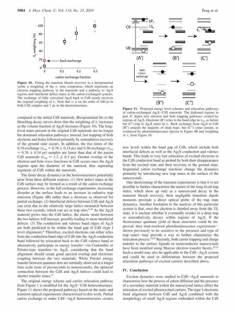
The original energy scheme and carrier relaxation pathwayfrom Figure 1 is modified for the Ag2S-CdS heterostructures.Figure 11 shows the proposed pathways based on the static andtransient optical experiments characterized in this work. Partialcation exchange to make CdS-Ag2S heterostructures creates
new levels within the band gap of CdS, which include bothinterfacial defects as well as the Ag2S conduction and valencebands. This leads to very fast relaxation of excited electrons inthe CdS conduction band as probed by both their disappearancefrom the excited state and their recovery to the ground state.Sequential cation exchange reactions change the dynamicsprimarily by introducing new trap states at the surface of thenanocrystals.
One shortcoming of the transient experiments is that it is notpossible to further characterize the nature of the long-lived trapstates, which show up only as a nanosecond decay in thetransient bleach recovery; their negligible transition dipolemoments preclude a direct optical probe of the trap statedynamics. Another limitation to the analysis of this particularsystem is that, once the electron is shuttled away from the 1Se
state, it is unclear whether it eventually resides in a deep trapor nonradiatively decays within regions of Ag2S. If thefluorescence quantum yield of these structures could be im-proved, then time-resolved photoluminescence experimentssshown previously to be sensitive to the presence and type oftrap statessmay provide a way to further characterize therelaxation process.14,22 Recently, both carrier trapping and chargetransfer to the surface ligands in semiconductor nanocrystalshave been modeled using Marcus electron transfer theory.22,32
Such a model may also be applicable to the CdS-Ag2S systemand could be used to differentiate between the proposedrelaxation pathways of excited carriers described above.
IV. Conclusion
Exciton dynamics were studied in CdS-Ag2S nanorods tocharacterize how the process of cation diffusion and the presenceof a secondary material within the nanocrystal lattice affect therelaxation of excited photoexcited carriers. The type I electronicband alignment between CdS and Ag2S combined with themorphology of small Ag2S regions embedded within the CdS
Figure 10. Fitting the transient bleach recovery to a biexponentialyields a weighting of the τ1 time component, which represents anelectron trapping pathway in the nanorods and a pathway to Ag2Sregions and interfacial defect states in the cation-exchanged systems.The exchange of fully converted Ag2S back to CdS nearly recoversthe original weighting of τ1. Note that τ1 is on the order of 100 ps inboth CdS samples and 1 ps in the heterostructures.
Figure 11. Proposed energy level schemes and relaxation pathwaysof cation-exchanged Ag2S-CdS nanorods. The darkened regions inpart A′ depict new electron and hole trapping pathways created byregions of Ag2S. Electrons (B′) relax to the band edge in τrise as beforebut (C′) trap to Ag2S states in τ1. Back exchange from Ag2S to CdS(B′′) anneals the majority of deep traps, but (C′′) some remain, asevidenced by photoluminescence spectra in Figure 4B and weightingof τ1 from Figure 10.
5884 J. Phys. Chem. C, Vol. 114, No. 13, 2010 Peng et al.

nanorods provides an interesting structure where visible lightabsorption in the wide band gap CdS material can produce near-infrared emission from the narrow gap Ag2S. While the fastdecay dynamics in the heterostructures suggest strong electroniccoupling between the CdS and Ag2S materials, it also indicatesthere is a significant amount of trap states (most likely interfacialdefects), which prevent radiative recombination from the Ag2Sband edges. One way to solve this problem may be to changethe composition of the heterostructure, while preserving itsmorphology. For instance, we have recently shown that theCdS-Ag2S nanorod heterostructures can be converted toCdS-PbS nanorods by a second exchange reaction.26 PbS alsohas a highly tunable direct band gap in the near-infrared whichmay improve the quantum yield of these types of nanocrystalheterostructures.7 Cation exchange provides a powerful routefor tuning the composition and resulting optical properties ofionic semiconductor nanocrystals. Further studies on the carrierdynamics in these materials can facilitate their application inoptoelectronic devices for light absorption (e.g., photovoltaics)and emission (e.g., light-emitting diodes and lasers).
Acknowledgment. The authors thank Dr. Gordana Dukovicand Dr. Prashant K. Jain for helpful discussions in preparingthe manuscript and Maxwell Merkle for measurement ofnanorod concentrations. The nanocrystal synthesis portion ofthis work, carried out by B.S. and supervised by A.P.A. andR.J.S., was supported by the Director, Office of Science, Officeof Basic Energy Sciences, Chemical and Materials SciencesDivisions, of the U.S. Department of Energy under ContractNo. DE-AC02-05CH1123. The spectroscopy experiments, car-ried out by P.P. and supervised by R.J.S., were supported bythe Experimental Physical Chemistry Division of the NationalScience Foundation under Grant No. CHE-0650950. P.P. wassupported by the NSF-IGERT foundation.
Supporting Information Available: Detailed descriptionsof the CdS nanorod synthesis and cation exchange reactions,size histograms of the nanorods, and transient bleaching andintraband absorption dynamics of the nanorods in the presenceof chemical quenchers. This material is available free of chargevia the Internet at http://pubs.acs.org.
References and Notes
(1) Bailey, R. E.; Nie, S. M. J. Am. Chem. Soc. 2003, 125, 7100–7106.
(2) Pradhan, N.; Goorskey, D.; Thessing, J.; Peng, X.-G. J. Am. Chem.Soc. 2005, 127, 17586–17587.
(3) Zhong, X.-H.; Feng, Y.-Y.; Zhang, Y.-L.; Gu, Z.-Y.; Zhou, L.Nanotechnology 2007, 18, 385606.
(4) Kim, S.; Fisher, B.; Eisler, H.-J.; Bawendi, M. J. Am. Chem. Soc.2003, 125, 11466–11467.
(5) Battaglia, D.; Blackman, B.; Peng, X.-G. J. Am. Chem. Soc. 2005,127, 10889–10897.
(6) Mews, A.; Eychmuller, A.; Giersig, M.; Schoss, D.; Weller, H. J.Phys. Chem. 1994, 98, 934–941.
(7) Pietryga, J. M.; Werder, D. J.; Williams, D. J.; Casson, J. L.;Schaller, R. D.; Klimov, V. I.; Hollingsworth, J. A. J. Am. Chem. Soc.2008, 130, 4879–4885.
(8) Robinson, R. D.; Sadtler, B.; Demchenko, D. O.; Erdonmez, C. K.;Wang, L.-W.; Alivisatos, A. P. Science 2007, 317, 355–358.
(9) Son, D.-H.; Hughes, S. M.; Yin, Y.-D.; Alivisatos, A. P. Science2004, 306, 1009–1012.
(10) Sadtler, B.; Demchenko, D. O.; Zheng, H.; Hughes, S. M.; Merkle,M. G.; Dahmen, U.; Wang, L.-W.; Alivisatos, A. P. J. Am. Chem. Soc.2009, 131, 5285–5293.
(11) Wark, S. E.; Hsia, C.-H.; Son, D.-H. J. Am. Chem. Soc. 2008, 130,9550–9555.
(12) Camargo, P. H. C.; Lee, Y.-H.; Jeong, U.; Zou, Z.-Q.; Xia, Y.Langmuir 2007, 23, 2985–2992.
(13) Chan, E. M.; Marcus, M. A.; Fakra, S.; ElNaggar, M.; Mathies,R. A.; Alivisatos, A. P. J. Phys. Chem. A 2007, 111, 12210–12215.
(14) Garrett, M. D.; Dukes, A. D., III; McBride, J. R.; Smith, N. J.;Pennycook, S. J.; Rosenthal, S. J. J. Phys. Chem. C 2008, 112, 12736–12746.
(15) Samia, A. C. S.; Lou, Y.; Burda, C.; Senter, R. A.; Coffer, J. L.J. Chem. Phys. 2004, 120, 8716–8723.
(16) Demchenko, D. O.; Robinson, R. D.; Sadtler, B.; Erdonmez, C. K.;Alivisatos, A. P.; Wang, L.-W. ACS Nano 2008, 2, 627–636.
(17) Owen, J. S.; Park, J.; Trudeau, P.-E.; Alivisatos, A. P. J. Am. Chem.Soc. 2008, 130, 12279–12281.
(18) Jones, G.; Jackson, W. R.; Halpern, A. M. Chem. Phys. Lett. 1980,72, 391–395.
(19) Klimov, V. I. J. Phys. Chem. B 2000, 104, 6112–6123.(20) Burda, C.; Link, S.; Mohamed, M.; El-Sayed, M. J. Phys. Chem.
B 2001, 105, 12286–12292.(21) Ramsden, J. J.; Gratzel, M. J. Chem. Soc., Faraday Trans. 1 1984,
80, 919–933.(22) Jones, M.; Lo, S.-S.; Scholes, G. D. Proc. Natl. Acad. Sci. U.S.A.
2009, 106, 3011–3016.(23) Guyot-Sionnest, P.; Shim, M.; Matranga, C.; Hines, M. Phys. ReV.
B 1999, 60, R2181–R2184.(24) Cavaleri, J. J.; Skinner, D. E.; Colombo, D. P.; Bowman, R. M.
J. Chem. Phys. 1995, 103, 5378–5386.(25) Motte, L.; Urban, J. J. Phys. Chem. B 2005, 109, 21499–21501.(26) Luther, J. M.; Zheng, H.; Sadtler, B.; Alivisatos, A. P. J. Am. Chem.
Soc. 2009, 131, 16851–16857.(27) Ninomiya, S.; Adachi, S. J. Appl. Phys. 1995, 78, 1183–1190.(28) Huxter, V. M.; Mirkovic, T.; Nair, P. S.; Scholes, G. D. AdV. Mater.
2008, 20, 2439–2443.(29) Junod, P.; Hediger, H.; Kilchor, B.; Wullschleger, J. Philos. Mag.
1977, 36, 941–958.(30) Li, L.-S.; Hu, J.-T.; Yang, W.-D.; Alivisatos, A. P. Nano Lett. 2001,
1, 349–351.(31) Achermann, M.; Petruska, M. A.; Crooker, S. A.; Klimov, V. I. J.
Phys. Chem. B 2003, 107, 13782–13787.(32) Hyun, B.-R.; Bartnik, A. C.; Lee, J.-K.; Imoto, H.; Sun, L.-F.; Choi,
J.-J.; Hanrath, T.; Ober, C. K.; Wise, F. W. Nano Lett. 2010, 10, 318–323.
JP9116722
Exciton Dynamics in CdS-Ag2S Nanorods J. Phys. Chem. C, Vol. 114, No. 13, 2010 5885