Embed Size (px)
Citation preview

_______________________________________________________________ Maxim Integrated Products 1
For pricing, delivery, and ordering information, please contact Maxim Direct at 1-888-629-4642, or visit Maxim’s website at www.maxim-ic.com.
3.3GHz to 3.9GHz MIMO Wireless Broadband RF Transceiver M
AX
28
42
19-5001; Rev 1; 5/10
Typical Operating Circuit appears at end of data sheet.
General DescriptionThe MAX2842 single-chip, direct-conversion, zero-IF RF transceiver IC is designed for 3GHz NLOS wireless broadband MIMO systems. It has two transmitters and two receivers, with differential 100I RF inputs and out-puts. The IC includes all circuitry required to implement the complete RF transceiver function, providing fully integrated receive paths, transmit path, VCO and tank, frequency synthesis, and baseband/control interface. It includes a fast-settling sigma-delta RF fractional synthe-sizer with ~25Hz frequency step size. The IC also inte-grates an on-chip AM detector for measuring transmitter I/Q imbalance and LO leakage. An internal transmit-to-receive loopback mode allows for receiver I/Q imbalance calibration. The IC supports full duplex mode of opera-tion for external loopback.
The MAX2842 completely eliminates the need for exter-nal SAW filters by implementing on-chip programmable monolithic filters for both receiver and transmitter, for channel bandwidths from 3.5MHz to 10MHz. The base-band filtering Rx and Tx signal paths are optimized to meet stringent noise figure and linearity requirements. The transceiver is housed in a small 56-pin TQFN, 7mm x 7mm, leadless plastic package with exposed paddle.
Applications3GHz 16d and 16e MIMO WiMAX
FeaturesS 3.3GHz to 3.9GHz Operation
S Complete RF Transceiver with PA Driver 0dBm Linear OFDMA Transmit Power, 64-QAM, -65dB Relative Spectral Emission Mask 3.8dB Receiver Noise Figure Automatic On-Chip Receiver I/Q DC Cancellation On-Chip Tx I/Q Gain/Phase Error and LO Leakage Detection Monolithic Low-Noise VCO with -38dBc Integrated Phase Noise Fully Integrated Programmable I/Q Lowpass Rx Channel Filters for 3.5MHz, 5MHz, 7MHz, and 10MHz Channels Programmable Tx I/Q Lowpass Reconstruction Filters Fractional PLL with 50µs Channel Hopping Time (Settling to 50Hz) 4-Wire Bidirectional SPI™ Interface 60dB Transmit Power Control Range, Digitally Controlled by SPI 71dB Receive Gain Control Range, Digitally Controlled by SPI RSSI with 60dB Dynamic Range Digital Control for Tx, Rx, Shutdown, and Standby Modes On-Chip Crystal Oscillator with Digital Tuning Programable Logic Interface Voltages Both Automatic and Modem-Assisted Receiver I/Q DC Offset Correction
S Single +2.7V to +3.6V Supply
S Low Shutdown Mode Current
S Small 56-Pin TQFN Package (7mm x 7mm)
Ordering Information
+Denotes a lead(Pb)-free/RoHS-compliant package.T = Tape and reel.*EP = Exposed pad.
SPI is a trademark of Motorola, Inc.
EVALUATION KIT
AVAILABLE
PART TEMP RANGE PIN-PACKAGE
MAX2842ETN+T -40NC to +85NC 56 TQFN-EP*

3.3GHz to 3.9GHz MIMO Wireless Broadband RF Transceiver
MA
X2
84
2
2 ______________________________________________________________________________________
Stresses beyond those listed under “Absolute Maximum Ratings” may cause permanent damage to the device. These are stress ratings only, and functional operation of the device at these or any other conditions beyond those indicated in the operational sections of the specifications is not implied. Exposure to absolute maximum rating conditions for extended periods may affect device reliability.
VCC_ Pins to GND ................................................-0.3V to +3.9VRF Inputs: Maximum Current at RXINA+, RXINA-, RXINB+, RXINB- ................................ -1mA to +1mARF Outputs: TXOUTA+, TXOUTA-, TXOUTB+, TXOUTB- to GND ..............................................-0.3V to +3.9VAnalog Inputs: TXBBIA+, TXBBIA-, TXBBQA+, TXBBQA-, TXBBIB+, TXBBIB-, TXBBQB+, TXBBQB-, REF_DIG to GND ..........-0.3V to +3.9VAnalog Input: XTAL1, REF_OSC .....................AC-Coupled OnlyAnalog Outputs: Maximum Current at RXBBIA+, RXBBIA-, RXBBQA+, RXBBQA-, RXBBIB+, RXBBIB-, RXBBQB+, RXBBQB-, CPOUT+, CPOUT- ......................... -1mA to +1mAAnalog Outputs: Maximum Current at PABIAS_A, PABIAS_B .............................. -100mA to +100mA
Digital Inputs: TXRX, CS, SCLK, DIN, ENABLE, CLKOUTEN to GND ..........................-0.3V to +3.9VDigital Outputs: DOUT, CLKOUT .........................-0.3V to +3.9VBias Voltages: BYP_VCO .....................................-0.3V to +3.9VShort-Circuit Duration on All Output Pins .............................. 10sRF Input Power: All RXIN_ .............................................+10dBmRF Output Differential Load VSWR: All TXOUT_ .................... 6:1Continuous Power Dissipation (TA = +85NC) 56-Pin TQFN (derate 27.8mW/NC above +70NC) .....< 2222mWOperating Temperature Range .......................... -40NC to +85NCJunction Temperature .....................................................+150NCStorage Temperature Range ............................ -65NC to +160NCLead Temperature (soldering, 10s) ................................+260NCSoldering Temperature (reflow) ......................................+260NC
DC ELECTRICAL CHARACTERISTICS TABLE(MAX2842 Evaluation Kit, VCC_ = 2.7V to 3.6V, TA = -40NC to +85NC, Rx set to the maximum gain. ENABLE and TXRX are set accord-ing to operating mode, CS = high, SCLK = DIN = low, no input signal at RF inputs, all RF inputs and outputs terminated into 50I, receiver baseband outputs are open. 90mVRMS differential I and Q signals (1MHz) applied to I and Q baseband inputs of transmitter in transmit mode, all registers set to recommended settings and corresponding test mode, unless otherwise noted. Typical values are at VCC_ = 2.8V, fLO = 3.6GHz, and TA = +25NC, unless otherwise noted. LOGIC_VREF = VCC_.) (Note 1)
ABSOLUTE MAXIMUM RATINGS
CAUTION! ESD SENSITIVE DEVICE
PARAMETER CONDITIONS MIN TYP MAX UNITSSupply Voltage, VCC 2.7 3.6 V
Supply Current
Shutdown mode 10 FA
Shutdown mode with 44.8MHz reference clock output 1.9 3.6
mA
Shutdown mode with crystal oscillator enabled and 44.8MHz reference clock output
2.9 5.0
Standby mode 35 50
Rx modeOne receiver on 77 96
Both receivers on 115 142
Tx mode One transmitter on 152 190
Both transmitters on 246 320
Receiver loopback I/Q calibration
One receiver on 125 155
Both receivers on 154 190
Transmitter calibration with AM detector
One transmitter on 119 148
Both transmitters on 181 230
Rx I/Q Output Common-Mode Voltage
D5:D4 = 00 in Local address 8 1.0
VD5:D4 = 01 in Local address 8 0.77 1.1 1.32
D5:D4 = 10 in Local address 8 1.2
D5:D4 = 11 in Local address 8 1.3

3.3GHz to 3.9GHz MIMO Wireless Broadband RF Transceiver
MA
X2
84
2
_______________________________________________________________________________________ 3
DC ELECTRICAL CHARACTERISTICS TABLE (continued)(MAX2842 Evaluation Kit, VCC_ = 2.7V to 3.6V, TA = -40NC to +85NC, Rx set to the maximum gain. ENABLE and TXRX are set accord-ing to operating mode, CS = high, SCLK = DIN = low, no input signal at RF inputs, all RF inputs and outputs terminated into 50I, receiver baseband outputs are open. 90mVRMS differential I and Q signals (1MHz) applied to I and Q baseband inputs of transmitter in transmit mode, all registers set to recommended settings and corresponding test mode, unless otherwise noted. Typical values are at VCC_ = 2.8V, fLO = 3.6GHz, and TA = +25NC, unless otherwise noted. LOGIC_VREF = VCC_.) (Note 1)
AC ELECTRICAL CHARACTERISTICS TABLE—Rx Mode(MAX2842 Evaluation Kit, VCC_ = 2.7V to 3.6V, TA = +25NC, fRF = 3.601GHz, fLO = 3.6GHz, baseband output signal frequency = 1MHz, receiver baseband I/Q output at 90mVRMS, REF_OSC frequency = 44.8MHz, ENABLE = TXRX = CS = high, SCLK = DIN = low. Lowpass filter is set to 10MHz RF channel BW, with power matching for the differential RF pins using the Typical Operating Circuit. RXBB_ pins are loaded with differential 10kI resistor and 10pF capacitance in parallel. Registers set to default settings and corresponding test mode, unless otherwise noted. Unmodulated single-tone RF input signal is used with specifications that normally apply over the entire operating conditions, unless otherwise indicated.) (Note 1)
PARAMETER CONDITIONS MIN TYP MAX UNITS
Tx Baseband Input Common-Mode Voltage Operating Range
To achieve at least +4dBm Tx output P - 1dB with maximum -3dB gain setting
0.5 1.2 V
Tx Baseband Input Bias Current Source current 10 25 FA
LOGIC INPUTS: TXRX, ENABLE, SCLK, DIN, CS, CLKOUTEN
Digital Input-Voltage High, VIHVCC - 0.4V
V
Digital Input-Voltage Low, VIL 0.4 V
Digital Input-Current High, IIH -1 +1 FA
Digital Input-Current Low, IIL -1 +1 FA
LOGIC OUTPUTS: DOUT, CLKOUT
Digital Output-Voltage High, VOH Sourcing 100FAVCC - 0.4V
V
Digital Output-Voltage Low, VOL Sinking 100FA 0.4 V
DOUT Voltage in Shutdown Mode or Disabled Mode
D7:D5 = 000 in Main address 22 VOL V
CLKOUT Voltage When Disabled VOL V
PARAMETER CONDITIONS MIN TYP MAX UNITS
RECEIVER SYSTEM: RF INPUT TO I/Q BASEBAND LOADED OUTPUT
RF Input Frequency Range 3.3 3.9 GHz
Peak-to-Peak Gain Variation Over RF Input Frequency Range
Tested at band edges and band center; at one tempera-ture
3 dB
S11 of RF Input Port All RF gains -10 dB
Total Voltage GainTA = -40NC to +85NC
Maximum gain; D7:D0 = 11111000 in Main address 2 for Rx1, in Main address 3 for Rx2
70 77
dBMinimum gain; D7:D0 = 00000111 in Main address 2 for Rx1, in Main address 3 for Rx2
6 14

3.3GHz to 3.9GHz MIMO Wireless Broadband RF Transceiver
MA
X2
84
2
4 ______________________________________________________________________________________
AC ELECTRICAL CHARACTERISTICS TABLE—Rx Mode (continued)(MAX2842 Evaluation Kit, VCC_ = 2.7V to 3.6V, TA = +25NC, fRF = 3.601GHz, fLO = 3.6GHz, baseband output signal frequency = 1MHz, receiver baseband I/Q output at 90mVRMS, REF_OSC frequency = 44.8MHz, ENABLE = TXRX = CS = high, SCLK = DIN = low. Lowpass filter is set to 10MHz RF channel BW, with power matching for the differential RF pins using the Typical Operating Circuit. RXBB_ pins are loaded with differential 10kI resistor and 10pF capacitance in parallel. Registers set to default settings and corresponding test mode, unless otherwise noted. Unmodulated single-tone RF input signal is used with specifications that normally apply over the entire operating conditions, unless otherwise indicated.) (Note 1)
PARAMETER CONDITIONS MIN TYP MAX UNITS
RF Gain Steps
From maximum RF gain to maximum RF gain - 8dB (D2:0 = 001 in Main address 2 for Rx1, in Main address 3 for Rx2)
8
dB
From maximum RF gain to maximum RF gain - 16dB (D2:0 = 010 in Main address 2 for Rx1, in Main address 3 for Rx2)
16
From maximum RF gain to maximum RF gain - 24dB (D2:0 = 011 in Main address 2 for Rx1, in Main address 3 for Rx2)
24
From maximum RF gain to maximum RF gain - 32dB (D2:0 = 110 in Main address 2 for Rx1, in Main address 3 for Rx2)
32
From maximum RF gain to maximum RF gain - 40dB (D2:0 = 111 in Main address 2 for Rx1, in Main address 3 for Rx2)
40
Gain Change Settling Time
Any RF or baseband gain change; signal amplitude set-tling to Q0.5dB of steady state, excludes I/Q path DC offset settling
300
nsAny RF or baseband gain change; signal amplitude set-tling to Q0.1dB of steady state, excludes I/Q path DC offset settling
500
Baseband Gain Range
From maximum baseband gain (D7:D3 = 00000 in Main address 2 for Rx1, in Main address 3 for Rx2) to mini-mum gain (D7:D3 = 11111 in Main address 2 for Rx1, in Main address 3 for Rx2)
28 31 34 dB
Baseband Gain Step Size 1 dB

3.3GHz to 3.9GHz MIMO Wireless Broadband RF Transceiver
MA
X2
84
2
_______________________________________________________________________________________ 5
AC ELECTRICAL CHARACTERISTICS TABLE—Rx Mode (continued)(MAX2842 Evaluation Kit, VCC_ = 2.7V to 3.6V, TA = +25NC, fRF = 3.601GHz, fLO = 3.6GHz, baseband output signal frequency = 1MHz, receiver baseband I/Q output at 90mVRMS, REF_OSC frequency = 44.8MHz, ENABLE = TXRX = CS = high, SCLK = DIN = low. Lowpass filter is set to 10MHz RF channel BW, with power matching for the differential RF pins using the Typical Operating Circuit. RXBB_ pins are loaded with differential 10kI resistor and 10pF capacitance in parallel. Registers set to default settings and corresponding test mode, unless otherwise noted. Unmodulated single-tone RF input signal is used with specifications that normally apply over the entire operating conditions, unless otherwise indicated.) (Note 1)
PARAMETER CONDITIONS MIN TYP MAX UNITS
DSB Noise FigureBalun input referred
Voltage gain R 65dB with maximum RF gain (D7:0 = 10111000 in Main address 2 for Rx1, in Main address 3 for Rx2)
3.8
dB
Voltage gain = 50dB with maximum RF gain - 8dB (D7:0 = 10000001 in Main address 2 for Rx1, in Main address 3 for Rx2)
7.1
Voltage gain = 45dB with maximum RF gain - 16dB (D7:0 = 10011010 in Main address 2 for Rx1, in Main address 3 for Rx2)
13.3
Voltage gain = 15dB with maximum RF gain - 32dB (D7:0 = 00101110 in Main address 2 for Rx1, in Main address 3 for Rx2)
28.2
Out-of-Band Input IP3
Two tones at +20MHz and +39MHz offsets, at -35dBm each; measure IM3 at 1MHz
AGC set for -65dBm wanted signal, maximum RF gain (D7:0 = xxxxx000 in Main address 2 for Rx1, in Main address 3 for Rx2)
-15
dBm
AGC set for -55dBm wanted signal, maximum RF gain - 8dB (D7:0 = xxxxx001 in Main address 2 for Rx1, in Main address 3 for Rx2)
-9
AGC set for -40dBm wanted signal, maximum RF gain - 16dB (D7:0 = xxxxx010 in Main address 2 for Rx1, in Main address 3 for Rx2)
-6
AGC set for -30dBm wanted signal, maximum RF gain - 32dB (D7:0 = xxxxx110 in Main address 2 for Rx1, in Main address 3 for Rx2)
0

3.3GHz to 3.9GHz MIMO Wireless Broadband RF Transceiver
MA
X2
84
2
6 ______________________________________________________________________________________
AC ELECTRICAL CHARACTERISTICS TABLE—Rx Mode (continued)(MAX2842 Evaluation Kit, VCC_ = 2.7V to 3.6V, TA = +25NC, fRF = 3.601GHz, fLO = 3.6GHz, baseband output signal frequency = 1MHz, receiver baseband I/Q output at 90mVRMS, REF_OSC frequency = 44.8MHz, ENABLE = TXRX = CS = high, SCLK = DIN = low. Lowpass filter is set to 10MHz RF channel BW, with power matching for the differential RF pins using the Typical Operating Circuit. RXBB_ pins are loaded with differential 10kI resistor and 10pF capacitance in parallel. Registers set to default settings and corresponding test mode, unless otherwise noted. Unmodulated single-tone RF input signal is used with specifications that normally apply over the entire operating conditions, unless otherwise indicated.) (Note 1)
PARAMETER CONDITIONS MIN TYP MAX UNITS
Out-of-Band Input IP2
Two tones at +50MHz and +51MHz offsets, at -40dBm each; measure IM2 at 1MHz
AGC set for -65dBm wanted signal, maximum RF gain (D7:0 = xxxxx000 in Main address 2 for Rx1, in Main address 3 for Rx2)
30 dBm
In-Band Input P-1dB
Maximum RF gain (D2:0 = 000 in Main address 2 for Rx1, in Main address 3 for Rx2)
-41
dBm
Maximum RF gain - 8dB (D2:0 = 001 in Main address 2 for Rx1, in Main address 3 for Rx2)
-32
Maximum RF gain - 16dB (D2:0 = 010 in Main address 2 for Rx1, in Main address 3 for Rx2)
-24
Maximum RF gain - 32dB (D2:0 = 110 in Main address 2 for Rx1, in Main address 3 for Rx2)
-8
Output P-1dB Compression Over passband frequency range, at minimum VGA gain 1.5 VP-P
I/Q Gain Imbalance 1MHz I/Q baseband output, 1s variation 0.05 dB
I/Q Phase Error 1MHz I/Q baseband output, 1s variation 0.5 Degrees
Loopback Gain (for Receiver I/Q Calibration)
Transmitter I/Q input to receiver I/Q output; transmitter gain at maximum - 6dB (D5:0 = 000110 in Main address 25), receiver baseband gain = maximum - 10dB (D7:3 = 10101 in Main address 2 for Rx1, in Main address 3 for Rx2) programmed through SPI (Note 2)
2 9 17 dB
I/Q DC Error After Receive Enable
Using one-shot mode, 7Fs after receive enable Q15 mV
I/Q Output DC DroopAveraged both over 10Fs, 5Fs to 10ms after any gain change or receive enable DC convergence, 1s variation
Q100 FV/ms
Isolation Between Rx Channel A and Rx Channel B
25 dB
RECEIVER BASEBAND FILTERS
RF Channel BW Supported by BB Filter
Main address 0, serial bits D2:D1 = 00 3.5
MHzMain address 0, serial bits D2:D1 = 01 5
Main address 0, serial bits D2:D1 = 10 7
Main address 0, serial bits D2:D1 = 11 10
Baseband Gain Ripple 0 to 4.6MHz for BW = 10MHz 1.7 dBP-P
Baseband Group Delay Ripple 0 to 4.6MHz for BW = 10MHz 42 nsP-P

3.3GHz to 3.9GHz MIMO Wireless Broadband RF Transceiver
MA
X2
84
2
_______________________________________________________________________________________ 7
AC ELECTRICAL CHARACTERISTICS TABLE—Rx Mode (continued)(MAX2842 Evaluation Kit, VCC_ = 2.7V to 3.6V, TA = +25NC, fRF = 3.601GHz, fLO = 3.6GHz, baseband output signal frequency = 1MHz, receiver baseband I/Q output at 90mVRMS, REF_OSC frequency = 44.8MHz, ENABLE = TXRX = CS = high, SCLK = DIN = low. Lowpass filter is set to 10MHz RF channel BW, with power matching for the differential RF pins using the Typical Operating Circuit. RXBB_ pins are loaded with differential 10kI resistor and 10pF capacitance in parallel. Registers set to default settings and corresponding test mode, unless otherwise noted. Unmodulated single-tone RF input signal is used with specifications that normally apply over the entire operating conditions, unless otherwise indicated.) (Note 1)
AC ELECTRICAL CHARACTERISTICS TABLE—Tx Mode(MAX2842 Evaluation Kit, VCC_ = 2.7V to 3.6V, TA = +25NC, fRF = 3.601GHz, fLO = 3.6GHz, REF_OSC frequency = 44.8MHz, ENABLE = CS = high, TXRX = SCLK = DIN = low. Power matching at RF outputs using the Typical Operating Circuit. Lowpass filter is set to 10MHz RF channel BW; 90mVRMS, 1MHz sine and cosine signal applied to I and Q baseband inputs of transmitter (differential DC-coupled). Registers set to default settings and corresponding test mode, unless otherwise noted.) (Note 1)
PARAMETER CONDITIONS MIN TYP MAX UNITS
Baseband Filter Stop Band Rejection
3.5MHz channel bandwidth
1.6MHz 0.5
dB
2.3MHz 5.5
14.25MHz 60
5MHz channel bandwidth
2.3MHz 0.5
3.3MHz 5.5
21MHz 60
7MHz channel bandwidth
3.2MHz 0.5
4.7MHz 5.5
29MHz 60
10MHz channel bandwidth
4.6MHz 0.5
6.7MHz 5.5
41.6MHz 60
RSSI
RSSI Minimum Output Voltage RLOAD = 10kI 0.5 V
RSSI Maximum Output Voltage RLOAD = 10kI 2.2 V
RSSI Slope 30 mV/dB
RSSI Output Settling Time To within 3dB of steady state +32dB signal step 400
ns-32dB signal step 1100
PARAMETER CONDITIONS MIN TYP MAX UNITS
TRANSMIT SECTION: Tx BASEBAND I/Q INPUTS TO RF OUTPUTS
RF Output Frequency Range 3.3 3.9 GHz
Peak-to-Peak Gain Variation Over RF Band
Single matching for entire band, at one temperature 2.2 dB
Total Voltage Gain At unbalanced 50I matched output 5 dB
Maximum Output Power OFDMA signal, gain adjusted over maximum gain and maximum gain - 6dB; single matching for entire band; 64-QAM, EVM = -36dB
0 dBm
RF Output Return Loss All gain settings 6 dB
Output P-1dB Maximum gain setting 10 dBm

3.3GHz to 3.9GHz MIMO Wireless Broadband RF Transceiver
MA
X2
84
2
8 ______________________________________________________________________________________
AC ELECTRICAL CHARACTERISTICS TABLE—Tx Mode (continued)(MAX2842 Evaluation Kit, VCC_ = 2.7V to 3.6V, TA = +25NC, fRF = 3.601GHz, fLO = 3.6GHz, REF_OSC frequency = 44.8MHz, ENABLE = CS = high, TXRX = SCLK = DIN = low. Power matching at RF outputs using the Typical Operating Circuit. Lowpass filter is set to 10MHz RF channel BW; 90mVRMS, 1MHz sine and cosine signal applied to I and Q baseband inputs of transmitter (differential DC-coupled). Registers set to default settings and corresponding test mode, unless otherwise noted.) (Note 1)
PARAMETER CONDITIONS MIN TYP MAX UNITS
RF Gain Control RangeFrom maximum Tx gain (D5:D0 = 000000 in Main address 25 for Tx1, in Main address 24 for Tx2) to mini-mum Tx gain (B6:B1 = 111111)
60 dB
Unwanted Sideband Suppression
Without calibration by modem, and excludes modem I/Q imbalance; sine and cosine signal applied to the I/Q baseband inputs
Maximum Tx gain 45dB
Minimum Tx gain 38
RF Gain Control Binary Weights
D0 in Main address 25 for Tx1, in Main address 24 for Tx2 1
dB
D1 in Main address 25 for Tx1, in Main address 24 for Tx2 2
D2 in Main address 25 for Tx1, in Main address 24 for Tx2 4
D3 in Main address 25 for Tx1, in Main address 24 for Tx2 8
D4 in Main address 25 for Tx1, in Main address 24 for Tx2 16
D5 in Main address 25 for Tx1, in Main address 24 for Tx2 32
Carrier LeakageRelative to -3dBm output power; without calibration by modem sine and cosine signal applied to the I/Q base-band inputs
-40 dBc
Tx I/Q Input Impedance (R||C)Differential resistance 25 kI
Differential capacitance 1 pF
Baseband Filter Rejection
3.5MHz channel bandwidth2.33MHz 0.5
dB
6.62MHz 45
5MHz channel bandwidth3.33MHz 0.5
9.45MHz 45
7MHz channel bandwidth4.67MHz 0.5
13.23MHz 45
10MHz channel bandwidth6.67MHz 0.5
18.9MHz 45
Baseband Group Delay Ripple 0 to 4.6MHz (BW = 10MHz) 10 ns
Baseband Input 1dB Gain Compression or Expansion
Sine and cosine signal applied to the I/Q baseband inputs, 5MHz I/Q inputs
0.5 VPEAK
Isolation Between Tx Channel A and Tx Channel B
45 dB
Maximum Gain Mismatch Between Tx Channel A and Tx Channel B over RF Frequency
3.3GHz to 3.9GHz, single matching for entire band Q2 dB
TRANSMITTER LO LEAKAGE AND I/Q CALIBRATION USING POWER DETECTOR: Tx I/Q BASEBAND INPUT TO RECEIVER I-CHANNEL MULTIPLEXED OUTPUT
Output AC-Coupling, -3dB Frequency
750 kHz
Baseband AC Amplifier Gain Range
Measure from minimum gain (D5:D4 = 00 in Main address 21) to maximum gain (D5:D4 = 11 in Main address 21)
30 dB
3.3GHz to 3.9GHz MIMO Wireless Broadband RF Transceiver
MA
X2
84
2
_______________________________________________________________________________________ 9
AC ELECTRICAL CHARACTERISTICS TABLE—Tx Mode (continued)(MAX2842 Evaluation Kit, VCC_ = 2.7V to 3.6V, TA = +25NC, fRF = 3.601GHz, fLO = 3.6GHz, REF_OSC frequency = 44.8MHz, ENABLE = CS = high, TXRX = SCLK = DIN = low. Power matching at RF outputs using the Typical Operating Circuit. Lowpass filter is set to 10MHz RF channel BW; 90mVRMS, 1MHz sine and cosine signal applied to I and Q baseband inputs of transmitter (differential DC-coupled). Registers set to default settings and corresponding test mode, unless otherwise noted.) (Note 1)
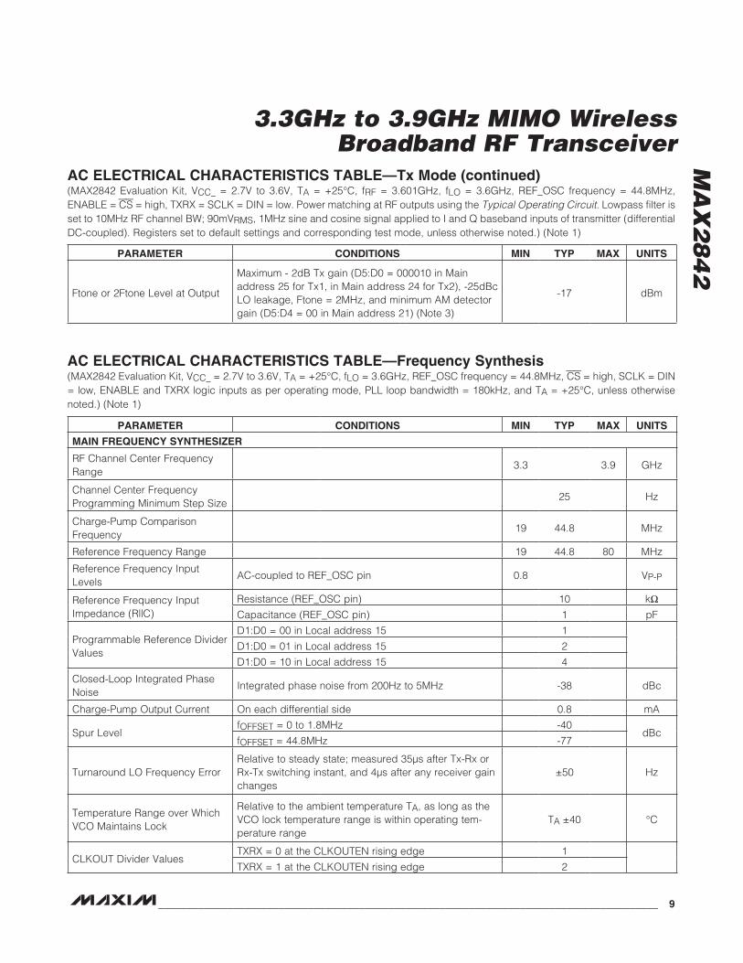
AC ELECTRICAL CHARACTERISTICS TABLE—Frequency Synthesis(MAX2842 Evaluation Kit, VCC_ = 2.7V to 3.6V, TA = +25NC, fLO = 3.6GHz, REF_OSC frequency = 44.8MHz, CS = high, SCLK = DIN = low, ENABLE and TXRX logic inputs as per operating mode, PLL loop bandwidth = 180kHz, and TA = +25NC, unless otherwise noted.) (Note 1)
PARAMETER CONDITIONS MIN TYP MAX UNITS
Ftone or 2Ftone Level at Output
Maximum - 2dB Tx gain (D5:D0 = 000010 in Main address 25 for Tx1, in Main address 24 for Tx2), -25dBc LO leakage, Ftone = 2MHz, and minimum AM detector gain (D5:D4 = 00 in Main address 21) (Note 3)
-17 dBm
PARAMETER CONDITIONS MIN TYP MAX UNITS
MAIN FREQUENCY SYNTHESIZER
RF Channel Center Frequency Range
3.3 3.9 GHz
Channel Center Frequency Programming Minimum Step Size
25 Hz
Charge-Pump Comparison Frequency
19 44.8 MHz
Reference Frequency Range 19 44.8 80 MHz
Reference Frequency Input Levels
AC-coupled to REF_OSC pin 0.8 VP-P
Reference Frequency Input Impedance (R||C)
Resistance (REF_OSC pin) 10 kI
Capacitance (REF_OSC pin) 1 pF
Programmable Reference Divider Values
D1:D0 = 00 in Local address 15 1
D1:D0 = 01 in Local address 15 2
D1:D0 = 10 in Local address 15 4
Closed-Loop Integrated Phase Noise
Integrated phase noise from 200Hz to 5MHz -38 dBc
Charge-Pump Output Current On each differential side 0.8 mA
Spur Level fOFFSET = 0 to 1.8MHz -40
dBcfOFFSET = 44.8MHz -77
Turnaround LO Frequency ErrorRelative to steady state; measured 35Fs after Tx-Rx or Rx-Tx switching instant, and 4Fs after any receiver gain changes
Q50 Hz
Temperature Range over Which VCO Maintains Lock
Relative to the ambient temperature TA, as long as the VCO lock temperature range is within operating tem-perature range
TA Q40 NC
CLKOUT Divider ValuesTXRX = 0 at the CLKOUTEN rising edge 1
TXRX = 1 at the CLKOUTEN rising edge 2

3.3GHz to 3.9GHz MIMO Wireless Broadband RF Transceiver
MA
X2
84
2
10 _____________________________________________________________________________________
AC ELECTRICAL CHARACTERISTICS TABLE—Frequency Synthesis (continued)(MAX2842 Evaluation Kit, VCC_ = 2.7V to 3.6V, TA = +25NC, fLO = 3.6GHz, REF_OSC frequency = 44.8MHz, CS = high, SCLK = DIN = low, ENABLE and TXRX logic inputs as per operating mode, PLL loop bandwidth = 180kHz, and TA = +25NC, unless otherwise noted.) (Note 1)
AC ELECTRICAL CHARACTERISTICS TABLE—Miscellaneous Blocks(MAX2842 Evaluation Kit, VCC_ = 2.7V to 3.6V, REF_OSC frequency = 44.8MHz, CS = high, SCLK = DIN = low, ENABLE and TXRX logic inputs as per operating mode, and TA = +25NC, unless otherwise noted.) (Note 1)
AC ELECTRICAL CHARACTERISTICS TABLE—Timing(MAX2842 Evaluation Kit, VCC_ = 2.7V to 3.6V, TA = +25NC, fLO = 3.6GHz, REF_OSC frequency = 44.8MHz, CS = high, SCLK = DIN = low, ENABLE and TXRX logic inputs as per operating mode, PLL loop bandwidth = 180kHz, and TA = +25NC, unless otherwise noted.) (Note 1)
PARAMETER CONDITIONS MIN TYP MAX UNITS
CLKOUT Output SwingR= 10kI, CLOAD = 5pF
D7:6 = 00 in Local address 9 with 44.8MHz clock output
2.56
VP-PD7:6 = 11 in Local address 9 with 22.4MHz clock output
2.66
PARAMETER CONDITIONS MIN TYP MAX UNITS
PA BIAS VOLTAGE
Output High Level 10mA source currentVCC -
0.2V
Output Low Level 10mA sink current 0.2 V
Turn-On TimeExcludes programmable delay of 0 to 6.3Fs in steps of 0.45Fs
200 ns
VCTCXO DAC
Output Current Source current
D5:D0 = 000000 in Main address 29
0
FAD5:D0 = 111111 in Main address 29
315
Maximum Output Voltage 2.4 V
Step Size 5 FA
ON-CHIP TEMPERATURE SENSOR
Digital Output CodeRead-out at DOUT pin through SPI
TA = +25NC 10001
TA = +85NC 11010
TA = -40NC 00101
Temperature Step Size 5 NC
PARAMETER SYMBOL CONDITIONS MIN TYP MAX UNITS
SYSTEM TIMING
Channel Switching TimeFrequency error settles to Q50Hz
Automatic VCO sub-band selection
2 ms
Manual VCO sub-band selection
56 Fs

3.3GHz to 3.9GHz MIMO Wireless Broadband RF Transceiver
MA
X2
84
2
______________________________________________________________________________________ 11
AC ELECTRICAL CHARACTERISTICS TABLE—Timing (continued)(MAX2842 Evaluation Kit, VCC_ = 2.7V to 3.6V, TA = +25NC, fLO = 3.6GHz, REF_OSC frequency = 44.8MHz, CS = high, SCLK = DIN = low, ENABLE and TXRX logic inputs as per operating mode, PLL loop bandwidth = 180kHz, and TA = +25NC, unless otherwise noted.) (Note 1)
Note 1: MAX2842 ICs are production tested at TA = +25NC. Min/max limits at TA = -40NC and TA = +85NC are guaranteed by design and characterization. There is no power-on register settings self-reset. Recommended register settings must be loaded after VCC is applied.
Note 2: Loopback gain is production tested at VCC_ = 2.7V. Min/max limits over the supply voltage range are guaranteed by design and characterization.
Note 3: The LO leakage produces Ftone, while the I/Q imbalance produces 2Ftone at the baseband output of the power detector. The output Ftone increases by 1dB for 1dB increase of the LO leakage, provided that the output power remains constant. The same relationship applies for the sideband leakage (due to I/Q imbalance) and 2Ftone.
PARAMETER SYMBOL CONDITIONS MIN TYP MAX UNITS
Turnaround Time
Measured from TXRX rising or falling edge; signal settling to within 0.5dB of steady state
Rx to Tx 2
Fs
Tx to Rx 2
Tx Turn-On Time (From Standby Mode)
Measured from ENABLE rising edge; signal settling to within 0.5dB of steady state
2 Fs
Tx Turn-Off Time (To Standby Mode)
From ENABLE falling edge 1 Fs
Rx Turn-On Time (From Standby Mode)
Measured from ENABLE rising edge; signal settling to within 0.5dB of steady state
2 Fs
Rx Turn-Off Time (To Standby Mode)
From ENABLE falling edge 1 Fs
4-WIRE SERIAL PARALLEL INTERFACE TIMING (See Figure 1)
SCLK Rising Edge to CS Falling Edge Wait Time
tCSO 6 ns
Falling Edge of CS to Rising Edge of First SCLK Time
tCSS 6 ns
DIN to SCLK Setup Time tDS 6 ns
DIN to SCLK Hold Time tDH 6 ns
SCLK Pulse-Width High tCH 6 ns
SCLK Pulse-Width Low tCL 6 ns
Last Rising Edge of SCLK to Rising Edge of CS or Clock to Load Enable Setup Time
tCSH 6 ns
CS High Pulse Width tCSW 45 ns
Time Between Rising Edge of CS and the Next Rising Edge of SCLK
tCS1 6 ns
Clock Frequency fCLK 45 MHz
Rise Time tR fCLK/10 ns
Fall Time tF fCLK/10 ns
SCLK Falling Edge to Valid DOUT
tD 12.5 ns

3.3GHz to 3.9GHz MIMO Wireless Broadband RF Transceiver
MA
X2
84
2
12 _____________________________________________________________________________________
Typical Operating Characteristics(VCC_ = 2.8V, TA = +25NC, fLO = 3.6GHz, fREF = REF_OSC frequency = 44.8MHz, CS = high, SCLK = DIN = low, ENABLE and TXRX logic inputs as per operating mode, RF BW = 10MHz, Tx output at 50I unbalanced output of balun, using the MAX2842 Evaluation Kit.)
FREQUENCY (GHz)
P OUT
(dBm
)
2.65GHz/div0 26.5
-120
-110
-100
-90
-80
-70
-60
-50
-40
-30
-130
MAX
2842
toc0
9Rx EMISSION SPECTRUM, LNA INPUT
(Tx OFF, LNA = MAX)Rx EVM vs. OFDM JAMMER
(10MHz CHANNEL BANDWIDTH, 64-QAM FUSC)
PJAMMER AT ANTENNA (dBm)
EVM
(%)
-30-40-70 -60 -50
2
4
6
8
10
12
14
16
0-80 -20
MAX
2842
toc0
8
fOFFSET = 10MHz
PWANTED = PSENSITIVITY + 3dB = -72.5dBmAT EVKIT INPUT. EVM AT PSENSITIVITY =5.85% WITHOUT JAMMER.
fOFFSET = 20MHz
VOUT (dBVRMS)
EVM
(%)
-10-15-30 -25 -20
2
4
6
8
10
12
14
16
0-35 -5
Rx EVM vs. VOUT (CHANNEL BANDWIDTH= 10MHz, 64-QAM FUSC)
MAX
2842
toc0
7
LNA = MAX - 32dBMINIMUM VGA GAIN.ADJUST VOUT BYINCREASING PIN.
LNA = MAX - 32dBADJUST VOUT BYINCREASING VGA GAIN.PIN = -22dBm(CONSTANT).
Rx EVM vs. PIN (CHANNEL BANDWIDTH= 10MHz, 64-QAM FUSC)
PIN (dBm)
EVM
(%)
-20-40-60-80
2
4
6
8
10
12
14
16
18
0-100 0
MAX
2842
toc0
6
LNA = MAX - 16dB
LNA = MAX - 24dB
LNA = MAX - 8dB
LNA = MAX
LNA = MAX - 32dB
LNA = MAX - 40dB
BASEBAND VGA CODE
VOLT
AGE
GAIN
(dB)
24168
10
20
30
40
50
60
70
80
90
00 32
Rx VOLTAGE GAIN vs.BASEBAND GAIN SETTING
MAX
2842
toc0
5
LNA = MAX
LNA = MAX - 8dB
LNA = MAX - 16dB
LNA = MAX - 24dB
LNA = MAX - 32dB
LNA = MAX - 40dB
Rx VOLTAGE GAIN (MAXIMUM LNAGAIN) vs. FREQUENCY
FREQUENCY (GHz)
GAIN
(dB)
3.83.73.63.53.4
72
74
76
78
80
703.3 3.9
MAX
2842
toc0
4
+85NC
+25NC
-40NC
Rx VOLTAGE GAIN vs. FREQUENCY
FREQUENCY (GHz)
GAIN
(dB)
3.83.73.63.53.4
40
50
60
70
80
303.3 3.9
MAX
2842
toc0
3
LNA = MAX
LNA = MAX - 8dB
LNA = MAX - 16dB
LNA = MAX - 24dB
LNA = MAX - 32dB
LNA = MAX - 40dB
NOISE FIGURE vs.BASEBAND GAIN SETTING
BASEBAND VGA ATTENUATION FROM MAX (dB)
NOIS
E FI
GURE
(dB)
24168
10
20
30
40
00 32
MAX
2842
toc0
2
LNA = MAX - 40dB
LNA = MAX - 32dB
LNA = MAX - 24dB
LNA = MAX - 16dB
LNA = MAX - 8dB
LNA = MAX
Rx SUPPLY CURRENT vs.SUPPLY VOLTAGE
SUPPLY VOLTAGE (V)
SUPP
LY C
URRE
NT (m
A)
3.33.0
112
114
116
118
120
122
124
126
1102.7 3.6
MAX
2842
toc0
1
+85NC
+25NC -40NC

3.3GHz to 3.9GHz MIMO Wireless Broadband RF Transceiver
MA
X2
84
2
______________________________________________________________________________________ 13
Typical Operating Characteristics (continued)(VCC_ = 2.8V, TA = +25NC, fLO = 3.6GHz, fREF = REF_OSC frequency = 44.8MHz, CS = high, SCLK = DIN = low, ENABLE and TXRX logic inputs as per operating mode, RF BW = 10MHz, Tx output at 50I unbalanced output of balun, using the MAX2842 Evaluation Kit.)
Rx BB FREQUENCY RESPONSE
FREQUENCY (MHz)
RESP
ONSE
(dB)
10
-70
-60
-50
-40
-30
-20
-10
0
10
-801 100
MAX
2842
toc1
8
CHANNEL BW = 10MHz
CHANNEL BW = 7MHz
CHANNEL BW = 5MHz
CHANNELBW = 3.5MHz
Rx DC OFFSET SETTING RESPONSE(TRIGGER AUTO DC CALIBRATION 400nsAFTER MAX TO MIN BB VGA GAIN STEP)
MAX2842 toc17
2V/div
100mV/div
0V
0V
1Fs/div
AUTO DC CAL TRIGGER
Rx OUTPUT
Rx DC OFFSET SETTING RESPONSE(TRIGGER AUTO DC CALIBRATION 400nsAFTER MIN TO MAX BB VGA GAIN STEP)
MAX2842 toc16
2V/div
0V
100mV/div
0V
1Fs/div
AUTO DC CAL TRIGGER
Rx OUTPUT
Rx LPF GROUP DELAY vs. FREQUENCY
MAX
2842
toc1
5
FREQUENCY (MHz)
LPF
GROU
P DE
LAY
(ns)
108642
50
100
150
200
250
300
350
400
450
500
00 12
CHANNEL BW = 3.5MHz
CHANNEL BW = 5MHz
CHANNEL BW = 7MHz
CHANNEL BW = 10MHz
Rx RSSI STEP RESPONSE(-40dB SIGNAL STEP)
MAX2842 toc14
2.8V
1.8V
0.6V
0V
200ns/div
LNA GAIN CONTROL
RSSI OUTPUT
Rx RSSI STEP RESPONSE(+40dB SIGNAL STEP)
MAX2842 toc13
2.8V
1.8V
0.6V
0V
200ns/div
LNA GAIN CONTROL
RSSI OUTPUT
RSSI VOLTAGE vs. INPUT POWER
PIN (dBm)
RSSI
VOL
TAGE
(V)
0-20-40-60-80
0.6
0.8
1.0
1.2
1.4
1.6
1.8
2.0
2.2
2.4
0.4-100 20
MAX
2842
toc1
2
LNA = MAX - 16dB
LNA = MAX- 8dB
LNA = MAX
LNA = MAX - 40dB
LNA = MAX - 32dB
LNA = MAX- 24dB
Rx INPUT RETURN LOSSvs. FREQUENCY
MAX
2842
toc1
1
FREQUENCY (GHz)
INPU
T RE
TURN
LOS
S (d
B)
3.83.73.63.53.4
-40
-35
-30
-25
-20
-15
-10
-5
0
-453.3 3.9
RxA LNA = MAX
RxB LNA = MAX - 40dB
RxB LNA = MAX
RxA LNA = MAX - 40dB
FREQUENCY (GHz)
REAL
COM
PONE
NT (I
)
IMAG
INAR
Y CO
MPO
NENT
(I)
3.93.83.73.63.53.43.3
40.5
41.0
41.5
42.0
42.5
43.0
40.0
-95
-90
-85
-80
-75
-70
-1003.2 4.0
Rx INPUT DIFFERENTIALIMPEDANCE vs. FREQUENCY
MAX2842 toc10
IMAGINARY
REAL

3.3GHz to 3.9GHz MIMO Wireless Broadband RF Transceiver
MA
X2
84
2
14 _____________________________________________________________________________________
Typical Operating Characteristics (continued)(VCC_ = 2.8V, TA = +25NC, fLO = 3.6GHz, fREF = REF_OSC frequency = 44.8MHz, CS = high, SCLK = DIN = low, ENABLE and TXRX logic inputs as per operating mode, RF BW = 10MHz, Tx output at 50I unbalanced output of balun, using the MAX2842 Evaluation Kit.)
Rx LNA GAIN STEP SETTLING RESPONSE(MIN - 32 TO MAX)
MAX2842 toc23
2.8V
100mV
-100mV
0V
200ns/div
LNA GAIN CONTROL
Rx OUTPUT
HISTOGRAM: Rx I/Q GAIN IMBALANCE MAX2842 toc24
MEAN = 0DEV = 39.6mdBSAMPLE SIZE = 3805
-0.5dB 0.5dB
MAX2842 toc26HISTOGRAM: Rx STATIC DC OFFSET
MEAN = 0DEV = 6.91mVSAMPLE SIZE = 3805
-50mV 50mV
MAX2842 toc25HISTOGRAM: Rx I/Q PHASE IMBALANCE
MEAN = 0DEV = 0.31°SAMPLE SIZE = 3805
-3.0° 3.0°
Rx LNA GAIN STEP SETTLING RESPONSE(MAX TO MIN - 8dB)
MAX2842 toc22
2.8V
100mV
-100mV
0V
200ns/div
LNA GAIN CONTROL
Rx OUTPUT
Rx VGA SETTLING RESPONSE(+16dB BB VGA GAIN STEP)
MAX2842 toc21
2.8V
100mV
-100mV
0V
200ns/div
VGA GAIN CONTROL
Rx OUTPUT
Rx VGA SETTLING RESPONSE(-16dB BB VGA GAIN STEP)
MAX2842 toc20
2.8V
100mV
-100mV
0V
200ns/div
VGA GAIN CONTROL
Rx OUTPUT
Rx BB FREQUENCY RESPONSEM
AX28
42 to
c19
FREQUENCY (MHz)
RESP
ONSE
(dB)
-5
-4
-3
-2
-1
0
1
2
-61 10
CHANNEL BW = 7MHz
CHANNELBW = 10MHz
CHANNELBW = 3.5MHz
CHANNEL BW = 5MHz

3.3GHz to 3.9GHz MIMO Wireless Broadband RF Transceiver
MA
X2
84
2
______________________________________________________________________________________ 15
Typical Operating Characteristics (continued)(VCC_ = 2.8V, TA = +25NC, fLO = 3.6GHz, fREF = REF_OSC frequency = 44.8MHz, CS = high, SCLK = DIN = low, ENABLE and TXRX logic inputs as per operating mode, RF BW = 10MHz, Tx output at 50I unbalanced output of balun, using the MAX2842 Evaluation Kit.)
TxB OUTPUT POWER vs. FREQUENCYM
AX28
42 to
c34
FREQUENCY (GHz)
P OUT
(dBm
)
3.83.73.4 3.5 3.6
-6
-5
-4
-3
-2
-1
0
1
-73.3 3.9
TA = +85NC
TA = +25NC
TA = -40NC
Tx GAIN SET TO MAX - 6dB
TxA OUTPUT POWER vs. FREQUENCY
MAX
2842
toc3
3
FREQUENCY (GHz)
P OUT
(dBm
)
3.83.73.4 3.5 3.6
-7
-6
-5
-4
-3
-2
-1
0
-83.3 3.9
TA = +85NC
TA = +25NC
TA = -40NC
Tx GAIN SET TO MAX - 6dB
Tx BASEBAND FREQUENCY RESPONSE
MAX
2842
toc3
2
FREQUENCY (MHz)
RESP
ONSE
(dB)
1
-5
-4
-3
-2
-1
0
1
2
-60.1 10
CHANNEL BW = 3.5MHz
CHANNEL BW = 5MHz
CHANNEL BW = 7MHz
CHANNEL BW = 10MHz
Tx BASEBAND FREQUENCY RESPONSE
MAX
2842
toc3
1
FREQUENCY (MHz)
RESP
ONSE
(dB)
101
-40
-30
-20
-10
0
10
-500.1 100
CHANNEL BW = 3.5MHz
CHANNEL BW = 5MHz
CHANNEL BW = 7MHz
CHANNEL BW = 10MHz
Tx SUPPLY CURRENTvs. SUPPLY VOLTAGE
MAX
2842
toc3
0
SUPPLY VOLTAGE (V)
SUPP
LY C
URRE
NT (m
A)
3.33.0
244
246
248
250
252
254
256
258
2422.7 3.6
TA = +25NC
TA = +85NC
TA = -40NC
Rx ISOLATION vs. FREQUENCY
MAX
2842
toc2
9
FREQUENCY (MHz)
ISOL
ATIO
N (d
B)
380037003400 3500 3600
22
24
26
28
30
32
34
36
203300 3900
RxB TO RxA
RxA TO RxB
POWER-ON DC OFFSET CANCELLATIONWITHOUT INPUT SIGNAL (TRIGGER AUTO
DC CALIBRATION 1µs AFTER ENABLE)MAX2842 toc28
2V/div
0V
0V
200mV/divRx OUTPUT
AUTO DC CAL TRIGGER
1Fs/div
POWER-ON DC OFFSET CANCELLATIONWITH INPUT SIGNAL (TRIGGER AUTO
DC CALIBRATION 1µs AFTER ENABLE)MAX2842 toc27
2V/div
0V
0V
500mV/divRx OUTPUT
AUTO DC CAL TRIGGER
1Fs/div

3.3GHz to 3.9GHz MIMO Wireless Broadband RF Transceiver
MA
X2
84
2
16 _____________________________________________________________________________________
Typical Operating Characteristics (continued)(VCC_ = 2.8V, TA = +25NC, fLO = 3.6GHz, fREF = REF_OSC frequency = 44.8MHz, CS = high, SCLK = DIN = low, ENABLE and TXRX logic inputs as per operating mode, RF BW = 10MHz, Tx output at 50I unbalanced output of balun, using the MAX2842 Evaluation Kit.)
Tx OUTPUT EMISSION SPECTRUMMAX2842 toc42
2.65GHz/div0 26.5FREQUENCY (GHz)
P OUT
(dBm
)
-90
-80
-70
-60
-50
-40
-30
-20
-10
0
fLO x 2
fLO x 4/3
fLO/3
fLO
MAX2842 toc43HISTOGRAM: Tx LO LEAKAGE
MEAN = -43.8dBcDEV = 4.62dBSAMPLE SIZE = 3805
-75dBc -15dBc
EVM vs. Tx OUTPUT POWER (64-QAM FUSC,10MHz CHANNEL BANDWIDTH)
MAX
2842
toc4
1
POUT (dBm)
EVM
(%)
0-10-20-30-40-50
0.50
1.00
1.50
2.00
2.50
3.00
3.50
0-60 10
Tx SIDEBAND SUPPRESSIONvs. GAIN SETTING
MAX
2842
toc4
0
Tx GAIN CODE
SS (d
Bc)
605040302010
-55
-50
-45
-40
-35
-600
TA = +25NC
TA = -40NC
TA = +85NC
Tx SIDEBAND SUPPRESSIONvs. FREQUENCY
MAX
2842
toc3
9
FREQUENCY (GHz)
SS (d
Bc)
3.83.73.63.53.4
-60
-55
-50
-45
-40
-653.3 3.9
TA = +85NC
TA = +25NC
TA = -40NC
Tx CARRIER SUPPRESSIONvs. GAIN SETTING
MAX
2842
toc3
8
Tx GAIN CODE
CS (d
Bc)
605030 402010
-65
-60
-55
-50
-45
-40
-35
-30
-25
-20
-700
TA = +85NC
TA = +25NC
TA = -40NC
Tx CARRIER SUPPRESSIONvs. FREQUENCY
MAX
2842
toc3
7
FREQUENCY (GHz)
CS (d
Bc)
3.83.73.63.53.4
-55
-50
-45
-40
-35
-30
-603.3 3.9
TA = +25NC
TA = +85NC
TA = -40NC
Tx OUTPUT SPECTRUM
MAX
2842
toc3
6
FREQUENCY (GHz)
POW
ER (d
Bm)
3.623.613.603.593.58
-90
-80
-70
-60
-50
-40
-30
-20
-10
-1003.57 3.63
Tx OUTPUT POWER vs. GAIN SETTING
MAX
2842
toc3
5
Tx GAIN CODE
P OUT
(dBm
)
605010 20 30 40
-60
-50
-40
-30
-20
-10
0
10
-700 70
TA = +85NC
TA = +25NC
TA = -40NC

3.3GHz to 3.9GHz MIMO Wireless Broadband RF Transceiver
MA
X2
84
2
______________________________________________________________________________________ 17
Typical Operating Characteristics (continued)(VCC_ = 2.8V, TA = +25NC, fLO = 3.6GHz, fREF = REF_OSC frequency = 44.8MHz, CS = high, SCLK = DIN = low, ENABLE and TXRX logic inputs as per operating mode, RF BW = 10MHz, Tx output at 50I unbalanced output of balun, using the MAX2842 Evaluation Kit.)
Tx OUTPUT RETURN LOSS vs. FREQUENCY
MAX
2842
toc4
6
FREQUENCY (GHz)
TxA
TxB
OUTP
UT R
ETUR
N LO
SS (d
B)
3.83.73.4 3.5 3.6
-14
-12
-10
-8
-6
-4
-2
0
-163.3 3.9
Tx ISOLATION vs. FREQUENCY
MAX
2842
toc4
5
FREQUENCY (MHz)
ISOL
ATIO
N (d
B)
38003700360035003400
42
44
46
48
50
52
54
56
58
60
403300 3900
TxA TO TxB
TxB TO TxA
MAX2842 toc44HISTOGRAM: Tx SIDEBAND SUPPRESSION
MEAN = -49.9dBcDEV = 4.9dBSAMPLE SIZE = 3805
-85dBc -25dBc
CHANNEL-SWITCHING FREQUENCY SETTLING(3.3GHz TO 3.9GHz,
AUTOMATIC VCO SUB-BAND SELECTION)MAX2842 toc52
10kHz/div
-50kHz0 3.2
50kHz
TIME (ms)
FREQUENCY ERROR
CHANNEL-SWITCHING FREQUENCY SETTLING(3.9GHz TO 3.3GHz,
MANUAL VCO SUB-BAND SELECTION)MAX2842 toc51
10kHz/div
-50kHz0 99.2
50kHz
TIME (Fs)
FREQUENCY ERROR
CHANNEL-SWITCHING FREQUENCY SETTLING(3.3GHz TO 3.9GHz,
MANUAL VCO SUB-BAND SELECTION)MAX2842 toc50
10kHz/div
-50kHz0 99.2
50kHz
TIME (Fs)
FREQUENCY ERROR
VCO GAIN vs. DIFFERENTIALTUNE VOLTAGE
MAX
2842
toc4
9
DIFFERENTIAL TUNE VOLTAGE (V)
VCO
GAIN
(MHz
/V)
2.01.51.00.5
100
200
300
400
500
600
700
00 2.5
PHASE NOISE vs. OFFSET FREQUENCYMAX2842 toc48-50
-60
-70
-80
-90
-100
-110
-120
-130
-140
-1500.0001 0.001 0.01 0.1 1 10
PHAS
E NO
ISE
(dBc
/Hz)
OFFSET FREQUENCY (MHz)
LO FREQUENCY vs. DIFFERENTIALTUNE VOLTAGE
MAX
2842
toc4
7
DIFFERENTIAL TUNE VOLTAGE (V)
LO F
REQU
ENCY
(GHz
)
2.01.61.20.80.4
3.5
4.0
4.5
5.0
5.5
3.00 2.4

3.3GHz to 3.9GHz MIMO Wireless Broadband RF Transceiver
MA
X2
84
2
18 _____________________________________________________________________________________
Pin Configuration
Typical Operating Characteristics (continued)(VCC_ = 2.8V, TA = +25NC, fLO = 3.6GHz, fREF = REF_OSC frequency = 44.8MHz, CS = high, SCLK = DIN = low, ENABLE and TXRX logic inputs as per operating mode, RF BW = 10MHz, Tx output at 50I unbalanced output of balun, using the MAX2842 Evaluation Kit.)
TOP VIEW
MAX2842
THIN QFN7mm x 7mm
+15
17
16
18
19
20
21
22
23
24
25
26
27
28
TXOUTB-
TXOUTB+
DOUT
SCLK
DIN
REF_DIG
CLKOUT
VCC_DIG
XTAL1
REF_OSC
XTAL_DAC
VCC_CP
CPOUT+
CPOUT-
RXINA+
RXINA-
GNDRXLNA_A
VCCRXLNA_A
TXRX
VCCMXR
TXBBQA-
TXBBQA+
TXBBIA+
TXBBIA-
RXBBIA+
RXBBIA-
RXBBQA+
RXBBQA-
48
47
46
45
44
43
54
53
56
55
52
51
50
*EP
*EXPOSED PADDLE.
49
1 2 3 4 5 6 7 8 9 10 11 12 13 14
42 41 40 39 38 37 36 35 34 33 32 31 30 29
V CCT
XMX_
B
PABI
AS_B
V CCT
XPAD
_BCS
PABI
AS_A
V CCT
XMX_
A
TXOU
TA+
TXOU
TA-
V CCT
XPAD
_A
ENAB
LE
RXIN
B+
RXIN
B-
GNDR
XLNA
_B
V CCR
XLNA
_B
V CC_
VCO
BYP_
VCO
GNDV
CO
CLKO
UTEN
RSSI
TXBB
IB-
TXBB
IB+
TXBB
QB+
TXBB
QB-
V CC_
BB
RXBB
IB-
RXBB
IB+
RXBB
QB-
RXBB
QB+
Tx-TO-Rx TURNAROUND FREQUENCYGLITCH SETTLING
MAX2842 toc55
5kHz/div
-25kHz0 49.6
25kHz
TIME (Fs)
FREQUENCY ERROR
Rx-TO-Tx TURNAROUND FREQUENCYGLITCH SETTLING
MAX2842 toc54
5kHz/div
-25kHz0 49.6
25kHz
TIME (Fs)
FREQUENCY ERROR
CHANNEL-SWITCHING FREQUENCY SETTLING(3.9GHz TO 3.3GHz,
AUTOMATIC VCO SUB-BAND SELECTION)MAX2842 toc53
10kHz/div
-50kHz0 3.2
50kHz
TIME (ms)
FREQUENCY ERROR

3.3GHz to 3.9GHz MIMO Wireless Broadband RF Transceiver
MA
X2
84
2
______________________________________________________________________________________ 19
Pin DescriptionPIN NAME FUNCTION
1 VCCRXLNA_B Receiver B LNA Supply Voltage. Bypass with a capacitor as close as possible to the pin.
2 GNDRXLNA_B Receiver B LNA Ground
3 RXINB- Receiver B LNA Differential Input. Inputs are internally DC-coupled. Two external series capacitors and one shunt inductor match the inputs to 100I differential.4 RXINB+
5 ENABLE Mode Control Logic Input. See Table 1 for operating modes.
6 VCCTXPAD_ATransmitter A Supply Voltage for Transmitter Power-Amplifier Driver. Bypass with a capacitor as close as possible to the pin.
7 TXOUTA- Transmitter A Power-Amplifier Driver Differential Output. The pins are internally DC-coupled. Two external series capacitors and one shunt inductor match the outputs to 100I differential.8 TXOUTA+
9 VCCTXMX_A Transmitter A Upconverter Supply Voltage. Bypass with a capacitor as close as possible to the pin.
10 PABIAS_A Transmit A External PA Bias Voltage Output
11 CS Chip-Select Logic Input of 4-Wire Serial Interface (See Figure 1)
12 VCCTXMX_B Transmitter B Upconverter Supply Voltage. Bypass with a capacitor as close as possible to the pin.
13 PABIAS_B Transmit B External PA Bias Voltage Output
14 VCCTXPAD_BTransmitter B Supply Voltage for Transmitter Power-Amplifier Driver. Bypass with a capacitor as close as possible to the pin.
15 TXOUTB- Transmitter B Power-Amplifier Driver Differential Output. The pins are internally DC-coupled. Two external series capacitors and one shunt inductor match the outputs to 100I differential.16 TXOUTB+
17 DOUT Data Logic Output of 4-Wire Serial Interface (See Figure 1)
18 SCLK Serial-Clock Logic Input of 4-Wire Serial Interface (See Figure 1)
19 DIN Data Logic Input of 4-Wire Serial Interface (See Figure 1)
20 REF_DIGCMOS Logic Supply-Voltage Reference Input. Bypass with a capacitor as close as possible to the pin. It is tested at 2.7V and 3.6V. For 1.8V voltage support, contact the manufacturer.
21 CLKOUT Divided Reference Clock Output
22 VCC_DIG Digital Blocks Supply Voltage. Bypass with a capacitor as close as possible to the pin.
23 XTAL1 Crystal Connection. (If the on-chip crystal oscillator is not used, leave this input unconnected.)
24 REF_OSC44.8MHz Reference Clock Input or Crystal Connection. AC-couple a crystal or a reference clock to this analog input.
25 XTAL_DAC Source Current DAC Output for VCTCXO
26 VCC_CP PLL Charge-Pump Supply Voltage. Bypass with a capacitor as close as possible to the pin.
27 CPOUT+ Differential Charge-Pump Output. Connect the frequency synthesizer’s loop filter between CPOUT+ and CPOUT- (see the Typical Operating Circuit).28 CPOUT-
29 GNDVCO VCO Ground
30 BYP_VCOOn-Chip VCO Regulator Output Bypass. Bypass with a 1FF capacitor to GND. Do not connect other circuitry to this point.
31 VCC_VCO VCO Supply Voltage. Bypass with a capacitor as close as possible to the pin.
32 CLKOUTEN Logic Input to Enable CLKOUT
33 RSSI RSSI or Temperature Sensor Multiplexed Analog Output
34 TXBBIB-Transmitter B Baseband I-Channel Differential Inputs
35 TXBBIB+
36 TXBBQB+Transmitter B Baseband Q-Channel Differential Inputs
37 TXBBQB-

3.3GHz to 3.9GHz MIMO Wireless Broadband RF Transceiver
MA
X2
84
2
20 _____________________________________________________________________________________
Pin Description (continued)PIN NAME FUNCTION
38 VCC_BB Receiver Baseband Supply Voltage. Bypass with a capacitor as close as possible to the pin.
39 RXBBIB- Receiver B Baseband I-Channel Differential Outputs. In Tx calibration mode, these pins are the LO leakage and sideband detector outputs.40 RXBBIB+
41 RXBBQB- Receiver B Baseband Q-Channel Differential Outputs. In Tx calibration mode, these pins are the LO leakage and sideband detector outputs.42 RXBBQB+
43 RXBBQA- Receiver A Baseband Q-Channel Differential Outputs. In Tx calibration mode, these pins are the LO leakage and sideband detector outputs.44 RXBBQA+
45 RXBBIA- Receiver A Baseband I-Channel Differential Outputs. In Tx calibration mode, these pins are the LO leakage and sideband detector outputs.46 RXBBIA+
47 TXBBIA-Transmitter A Baseband I-Channel Differential Inputs
48 TXBBIA+
49 TXBBQA+Transmitter A Baseband Q-Channel Differential Inputs
50 TXBBQA-
51 VCCMXR Receiver Downconverters Supply Voltage. Bypass with a capacitor as close as possible to the pin.
52 TXRX Mode Control Logic Input. See Table 1 for operating modes.
53 VCCRXLNA_A Receiver A LNA Supply Voltage. Bypass with a capacitor as close as possible to the pin.
54 GNDRXLNA_A Receiver A LNA Ground
55 RXINA- Receiver A LNA Differential Input. Inputs are internally DC-coupled. Two external series capacitors and one shunt inductor match the inputs to 100I differential.56 RXINA+
— EP (GND)Exposed Paddle Ground. Internally connected to ground. Connect to a large ground plane for opti-mum RF performance and enhanced thermal dissipation. Do not share with other pin grounds and bypass capacitors’ ground.

3.3GHz to 3.9GHz MIMO Wireless Broadband RF Transceiver
MA
X2
84
2
______________________________________________________________________________________ 21
Detailed DescriptionModes of Operation
The modes of operation for the MAX2842 are shutdown, clock-out, standby, Tx, Rx, Tx calibration, and Rx calibra-tion. See Table 1 for a summary of the modes of opera-tion. The logic input pins—TXRX (pin 52) and ENABLE (pin 5)—control the various modes.
Shutdown ModeCurrent drain is the minimum possible with the supply voltages applied. All circuit blocks are powered down, except the 4-wire serial bus and its internal program-mable registers. If the digital supply voltage is applied at the VCCDIG pin, the registers may be loaded.
Clock-Out Only ModeOnly the clock-out signal is active on the CLKOUT pin. The clock output divider is also functional. The rest of the transceiver is powered down.
The reference and CLKOUT can be configured by dif-ferent pins (ENABLE, TXRX, DIN, and CS) at the rising edge of the CLKOUTEN pin. After the rising edge of the CLKOUTEN pin, all logic pins will not change the state of the crystal oscillator and CLKOUT signal. Table 2 sum-marizes how different parameters are configured.
For operation that does not need CLKOUT to be avail-able, the reference buffer/crystal oscillator can be con-figured at the CLKOUTEN rising edge. The CLKOUT sig-nal can then be disabled by applying CLKOUTEN = “0.”
Standby ModePLL, VCO, and LO Gen blocks are generally on, so that Tx or Rx modes can be quickly enabled from this mode. These and other blocks may be selectively enabled or disabled in this mode. CLKOUT is enabled using the CLKOUTEN pin.
Table 1. Operating Mode Table
X = Don’t care.
Note 1: State “10” of SPI Main register 22, D1:D0 is the same as state “00” but not tested, and therefore should not be used.Note 2: CLKOUT signal is active independent of the states of SPI register 22, D1:D0. Clock divide ratio and on-chip crystal oscil-
lator are configured by different pins during power-up or rising edge of CLKOUTEN pin. See the Clock-Out Only Mode section in the Detailed Description for details.
Note 3: PA bias blocks may be selectively enabled in all modes except SHUTDOWN and CLKOUT.Note 4: Set Main register 0, D5 = 1 to enable both RxA and RxB. Set Main register 0, D5 = 0 to enable only RxA.Note 5: Set Main register 22, D2 = 1 to enable both TxA and TxB. Set Main register 22, D2 = 0 to enable only TxA.Note 6: Set SPI Main register 6, D9 = 1 to mux AM detector output to RXBB_ pins.Note 7: Set SPI Main register 22, D3 = 1 to calibrate TxA; set Main register 22, D3 = 0 to calibrate TxB.
MODE CONTROL LOGIC INPUTS CIRCUIT BLOCK STATES
MODE
SPI MAIN REGISTER 22, D1:D0(Note 1)
ENABLE PIN
TXRX PIN
CLKOUTEN PIN
Rx PATH Tx PATHPLL, VCO
CLOCK OUT
CALIBRATION SECTIONS ON
SHUTDOWN 00 0 0 0 Off Off Off Off None
CLKOUT(Note 2)
00 0 0 1 Off Off Off On None
STANDBY 01 0 1 X OffOff
(Note 3)On On/Off None
Rx(Note 4)
01 1 1 X On Off On On/Off None
Tx(Note 5)
01 1 0 X Off On On On/Off None
Tx Calibration(Notes 6, 7)
11 1 0 X OffOn (except PA driver)
On On/OffAM detector + Rx I/Q buffers
Rx Calibration 11 1 1 XOn
(except LNA)On (except PA driver)
On On/Off Loopback

3.3GHz to 3.9GHz MIMO Wireless Broadband RF Transceiver
MA
X2
84
2
22 _____________________________________________________________________________________
Rx ModeAll Rx circuit blocks are powered on and active. The antenna signal is applied; RF is downconverted, filtered, and buffered at the Rx baseband I and Q outputs. The slow-charging Tx circuits are in a precharged “idle-off” state for fast Rx-to-Tx turnaround time. CLKOUT is enabled using the CLKOUTEN pin.
Tx ModeAll Tx circuit blocks are powered on. The external PA is powered on after a programmable delay. The Tx driver amplifier is ramped from the low-gain state (minimum RF output) to the programmed high-gain state. The slow-charging Rx circuits are in a precharged “idle-off” state for fast Tx-to-Rx turnaround time. CLKOUT is enabled using the CLKOUTEN pin.
Tx Calibration ModeAll Tx circuit blocks except the PA driver and external PA are powered on and active. The AM detector and receiv-er I/Q channel buffers are also on, along with multipexers in the receiver side to route this AM detector’s signal to each I and Q differential line. The output of the Tx VGA is fed to the AM detector, so the PA driver gain steps will not affect this calibration signal path gain. CLKOUT is enabled using the CLKOUTEN pin.
Rx Calibration ModePart of the Rx and Tx circuit blocks, except the LNA and PA driver, are powered on and active. The transmitter I/Q input signal is upconverted to RF, and at the output of the Tx gain control (VGA) it is fed to the receiver at the input of the downconverter. Either or both of the two receiver channels can be connected to the transmitter and pow-ered on. The I/Q lowpass filters are not present in the
transmitter signal path (they are bypassed). The PA driver gain steps (part of the Tx gain control range) are not intended to affect the loopback signal level. CLKOUT is enabled using the CLKOUTEN pin.
Power-On SequencesTo ensure proper operation from power-down, the user needs to:
1) Enable the crystal oscillator, and wait at least 2ms.
2) Program the IC into standby mode and wait 2ms for frequency acquisition (56Fs if manual VCO sub-band selection is used).
3) Program the IC into Rx or Tx mode for normal operation.
4) In Rx mode, the user needs to first trigger automatic DC calibration with SPI and wait 5Fs for settling.
Programmable Registers and 4-Wire SPI Interface
The MAX2842 includes 55 programmable 16-bit regis-ters. There are 32 Main registers and 23 Local registers. The most significant bit (MSB) is the read/write selec-tion bit (R/W in Figure 1). The next 5 bits are a register address (A4:A0 in Figure 1). The 10 least significant bits (LSBs) are register data (D9:D0 in Figure 1). Register data is loaded through the 4-wire SPI/MICROWIRE™-compatible serial interface. The MSB of data at the DIN pin is shifted in first and is framed by CS. When CS is low, the clock is active, and input data is shifted at the rising edge of the clock at the SCLK pin. At the CS rising edge, the 10-bit data bits are latched into the register selected by the address bits. See Figure 1. To support more than a 32-register address using a 5-bit wide address word, the bit 9 of address 0 is used to select whether the 5-bit
Table 2. CLKOUT Divide Ratio, Crystal Oscillator/Reference Buffer, and Oscillator Bias Selection During CLKOUTEN Pin Rising Edge*
*The above selection cannot be programmed through SPI.
MICROWIRE is a trademark of National Semiconductor Corp.
PIN LEVEL SELECT NOTE
TXRX atCLKOUTEN Rising Edge
0 Divide-by-1 —
1 Divide-by-2 —
ENABLE atCLKOUTEN Rising Edge
0 Disable on-chip crystal oscillator Works as a reference buffer
1 Enable on-chip crystal oscillator —
CS, DIN at CLKOUTEN Rising Edge (Only Needed When Crystal Oscillator Is Active)
11
40MHz 50I max
38.4MHz 50I max
52MHz 50I max
44.8MHz 50I max

3.3GHz to 3.9GHz MIMO Wireless Broadband RF Transceiver
MA
X2
84
2
______________________________________________________________________________________ 23
address word is applied to the main address or local address. The register values are preserved in shutdown mode as long as the power-supply voltage is maintained. There is no guaranteed power-on SPI register self-reset functionality in the MAX2842; the user must program all register values after power-up. During the read mode, register data selected by the address bits is shifted out to the DOUT pin at the falling edges of the clock.
SPI Register DefinitionAll values in register definition tables are typical num-bers. The MAX2842 SPI does not have a power-on-default self-reset feature; the user must program all SPI addresses for normal operation. Prior to the use of any untested settings, contact the factory.
Figure 1. 4-Wire SPI Serial-Interface Timing Diagram
Table 3. MAX2842 Register Summary
SCLK
tCSO
tCSS
tDS tDH
tCH
tCL
tCSW
tCSH
tCS1
A4R/W A0 D9 D0 DON’T CARE
A0 D9 D0A4R/W
DIN(SPI WRITE) DON’T CARE
DON’T CARE D9DOUT
(SPI READ)
DIN(SPI READ)
D0 DON’T CARE
CS
tD
REGISTER
WRITE/READ AND
ADDRESSDATA
MAIN0
D9A4:A0
WRITE/
READD9 D8 D7 D6 D5 D4 D3 D2 D1 D0
Main0 0 00000W/R
SPI_
program_
sel
RSSI_
Rxsel_SPIRSSI_MUX* RESERVED
MIMO_
mode_selts_en
ts_adc_
triggerFT[1:0] LNAband
Default 0 1 0 0 1 0 0 1 1 0
Main1 0 00001 Default 0 0 0 0 0 0 0 0 0 0
Main2 0 00010W/R
dccal_
word_sel_A*RESERVED VGA1[4:0] LNA1_GAIN[2:0]
Default 0 1 1 1 1 1 1 0 0 0

3.3GHz to 3.9GHz MIMO Wireless Broadband RF Transceiver
MA
X2
84
2
24 _____________________________________________________________________________________
Table 3. MAX2842 Register Summary (continued)
REGISTER
WRITE/READ AND
ADDRESSDATA
MAIN0
D9A4:A0
WRITE/
READD9 D8 D7 D6 D5 D4 D3 D2 D1 D0
Main3 0 00010W/R
dccal_
word_sel_BRESERVED VGA2[4:0] LNA2_GAIN[2:0]
Default 0 1 1 1 1 1 1 0 0 0
Main4 0 00100W/R RESERVED RESERVED RESERVED RESERVED RESERVED RESERVED RESERVED Iclkdiv* RESERVED RESERVED
Default 0 0 0 1 0 0 1 1 0 0
Main5 0 00101 Default 1 1 0 0 0 0 0 0 0 0
Main6 0 00110W/R sel_In1_In2 RESERVED RESERVED RESERVED RESERVED RESERVED RESERVED RESERVED RESERVED RESERVED
Default 0 1 0 0 0 0 0 0 0 0
Main70 00111 W/R
gain_
cntrl_2RXRESERVED RESERVED RESERVED RESERVED RESERVED RESERVED RESERVED RESERVED RESERVED
Default 0 1 0 0 0 0 0 0 0 0
Main8 0 01000 Default 0 1 0 0 0 0 0 0 0 0
Main9 0 01001 Default 1 1 0 0 0 0 0 0 0 0
Main10 0 01010W/R
dccal_
auto_enRESERVED RESERVED RESERVED RESERVED RESERVED RESERVED RESERVED RESERVED RESERVED
Default 0 1 0 0 0 0 0 0 0 0
Main11 0 01011 Default 0 1 0 0 0 0 0 0 0 0
Main12 0 01100 Default 0 1 0 0 0 0 0 0 0 0
Main13 0 01101 Default 0 0 0 0 0 0 0 0 0 0
Main14 0 01110 Default 0 0 0 0 0 0 0 0 0 0
Main15 0 01111 Default 0 0 0 0 0 0 0 0 0 0
Main16 0 10000 Default 0 0 0 0 0 0 0 0 0 0
Main17 0 10001 Default 0 0 0 0 0 0 0 0 0 0
Main18 0 10010 Default 0 0 0 0 0 0 0 0 0 0
Main19 0 10011 Default 0 0 0 0 0 0 0 0 0 0
Main20 0 10100 Default 0 0 0 0 0 0 0 0 0 0
Main21 0 10101
W RESERVED RESERVED RESERVED RESERVED TXCAL_GAIN[1:0] RESERVED RESERVED RESERVED RESERVED
R DIE_ID[2:0] REVISION_ID[2:0]
Default 0 0 1 1 0 0 0 0 0 0
Main22 0 10110 W/R RESERVED RESERVED DOUT_SEL[2:0]DOUT_
CSB_SEL*
TX_AMD_
SEL
TX_MIMO_
SELCAL_SPI EN_SPI
Default 0 0 0 0 0 0 0 1 0 0
Main23 0 10111 Default 0 0 1 0 0 0 0 0 0 0
Main24 0 11000W/R
PABIAS_
VMODE_B
PABIAS_
TX_EN_BRESERVED RESERVED TXGAIN_SPI_B[5:0]
Default 1 0 0 0 1 1 1 1 1 1
Main25 0 11001W/R
PABIAS_
VMODE_A
PABIAS_
TX_EN_ARESERVED RESERVED TXGAIN_SPI_A[5:0]
Default 1 0 0 0 1 1 1 1 1 1

3.3GHz to 3.9GHz MIMO Wireless Broadband RF Transceiver
MA
X2
84
2
______________________________________________________________________________________ 25
Table 3. MAX2842 Register Summary (continued)
REGISTER
WRITE/READ AND
ADDRESSDATA
MAIN0
D9A4:A0
WRITE/
READD9 D8 D7 D6 D5 D4 D3 D2 D1 D0
Main26 0 11010W/R SYN_CONFIG0[9:0]
Default 0 1 0 1 0 1 0 1 0 1
Main27 0 11011W/R SYN_CONFIG0[19:10]
Default 0 1 0 1 0 1 0 1 0 1
Main28 0 11100W/R
VAS_
TRIG_EN*SYN_CONFIG1[8:0]
Default 1 0 0 1 1 1 0 1 0 0
Main29 0 11101W/R RESERVED RESERVED XTAL_TUNE[7:0]
Default 1 0 0 0 0 0 0 0 0 0
Main30 0 11110
W LOGEN_BAND[1:0]
VAS_
RELOCK_
SEL*
VAS_MODE VAS_SPI[5:0]
R VAS_ADC[2:0] VCO_BSW[5:0]
Default 0 1 0 1 0 1 1 1 1 1
Main31 0 11111 Default 1 1 1 1 0 1 0 1 0 0
Local1 1 00001 Default 1 0 0 0 0 0 0 0 0 0
Local2 1 00010 Default 0 0 0 0 0 0 0 0 0 1
Local3 1 00011 Default 1 0 1 0 0 1 1 0 1 0
Local4 1 00100 Default 0 1 0 0 0 0 0 0 1 0
Local5 1 00101 Default 0 1 1 0 1 1 0 0 0 0
Local6 1 00110 Default 0 0 1 0 0 0 0 0 0 0
Local7 1 00111
W RESERVED RESERVED RESERVED RESERVED RESERVED
R RESERVED RESERVED RESERVED RESERVED RESERVED ts_adc[4:0]
Default 0 0 0 0 0 0 0 0 0 0
Local8 1 01000 Default 1 0 0 0 0 0 0 1 0 1
Local9 1 01001W/R RESERVED
XTAL_
DAC_ENCLKOUT_DRV[1:0] RESERVED RESERVED RESERVED RESERVED RESERVED RESERVED
Default 1 0 0 0 0 0 1 1 1 1
Local10 1 01010 Default 0 0 0 1 0 0 1 0 1 1
Local11 1 01011 Default 0 0 0 0 0 1 0 0 0 0
Local12 1 01100 Default 0 0 1 0 0 0 0 0 0 0
Local13 1 01101 Default 0 0 0 0 0 0 0 0 0 0
Local14 1 01110W/R RESERVED RESERVED RESERVED RESERVED RESERVED
PADAC_
DIVH*PADAC_DLY[3:0]
Default 0 0 1 0 1 1 0 0 1 1
Local15 1 01111W/R RESERVED RESERVED RESERVED RESERVED RESERVED
LOGEN_
2GMRESERVED RESERVED REF_DIV[1:0]
Default 1 1 0 1 0 0 0 1 0

3.3GHz to 3.9GHz MIMO Wireless Broadband RF Transceiver
MA
X2
84
2
26 _____________________________________________________________________________________
Table 3. MAX2842 Register Summary (continued)
Table 4. Main Address 0 (A4:A0 = 00000)
*These bits are not production tested. For functionality support, contact the manufacturer.
REGISTER
WRITE/READ AND
ADDRESSDATA
MAIN0
D9A4:A0
WRITE/
READD9 D8 D7 D6 D5 D4 D3 D2 D1 D0
Local16 1 10000W/R
VAS_VCO_
READOUT
DIE_ID_
READRESERVED RESERVED RESERVED RESERVED RESERVED RESERVED RESERVED RESERVED
Default 0 1 0 0 0 0 0 0 0 0
Local17 1 10001 Default 0 0 0 0 0 0 1 0 0 0
Local18 1 10010 Default 0 0 0 0 0 0 0 0 0 0
Local19 1 10011 Default 0 0 0 0 0 0 0 0 0 0
Local20 1 10100 Default 0 0 0 0 0 0 0 0 0 0
Local21 1 10101 Default 0 0 0 0 0 0 0 0 0 0
Local26 1 11010 Default 0 0 0 0 0 0 0 0 1 1
Local27 1 11011 Default 0 0 0 0 1 0 0 0 0 1
BIT NAMEBIT LOCATION
(D0 = LSB)DESCRIPTION
SPI_program_sel D9Select to program main or local registers for each address except for address 0.0 = Program main registers (default)1 = Program local registers
RSSI_RXsel_SPI D8Select RSSI input.0 = Select input from RxB1 = Select input from RxA (default)
RSSI_MUX D7
RSSI pin output mux. This bit is not production tested. For functionality support, contact the manufacturer.0 = RSSI (default)1 = Temperature sensor
RESERVED D6 Reserved bits—set to default
MIMO_mode_sel D5Rx MIMO mode selection.0 = Only RxA is active1 = Both RxA and RxB are active (default)
ts_en D4Temperature sensor comparator and clock enable.0 = Disable (default)1 = Enable
ts_adc_trigger D3Temperature sensor ADC trigger.0 = Not trigger ADC read-out (default)1 = Trigger ADC read-out. ADC is disabled automatically after read-out finishes.
FT[1:0] D2:D1
LPF RF bandwidth.00 = 3.5MHz01 = 5.0MHz10 = 7.0MHz11 = 10.0MHz (default)
LNAband D0Select center frequency of LNA output LC tank.LNAband = 0 3.3GHz~3.6GHz (default)LNAband = 1 3.6GHz~3.9GHz

3.3GHz to 3.9GHz MIMO Wireless Broadband RF Transceiver
MA
X2
84
2
______________________________________________________________________________________ 27
Table 5. Main Address 2 (A4:A0 = 00010, Main Address 0 D9 = 0)
Table 6. Main Address 3 (A4:A0 = 00011, Main Address 0 D9 = 0)
BIT NAMEBIT LOCATION
(D0 = LSB)DESCRIPTION
dccal_word_sel_A D9
Select which VGA DC offset word to use for RxA. This bit is not production tested. For functionality support, contact the manufacturer.0 = Use VGA DC offset word 1 (default)1 = Use VGA DC offset word 2
RESERVED D8 Reserved bits—set to default
VGA1[4:0] D7:D3
Set attenuation in RxA VGA.00000 = Minimum gain
00001 = Minimum gain + 1dB…11111 = Maximum gain (default)
LNA1_GAIN[2:0] D2:D0
RxA LNA gain-setting SPI controls.000 = Maximum gain (default)001 = -8dB from maximum gain010 = -16dB from maximum gain011 = -24dB from maximum gain100 = Not tested101 = Not tested110 = -32dB from maximum gain111 = -40dB from maximum gain
BIT NAMEBIT LOCATION
(D0 = LSB)DESCRIPTION
dccal_word_sel_B D9
Select which VGA DC offset word to use for RxB. This bit is not production tested. For functionality support, contact the manufacturer.0 = Use VGA DC offset word 1 (default)1 = Use VGA DC offset word 2
RESERVED D8 Reserved bits—set to default
VGA2[4:0] D7:D3
Set attenuation in RxB VGA.00000 = Minimum gain00001 = Minimum gain + 1dB…11111 = Maximum gain (default)
LNA2_GAIN[2:0] D2:D0
RxB LNA gain-setting SPI controls.000 = Maximum gain (default)001 = -8dB from maximum gain010 = -16dB from maximum gain011 = -24dB from maximum gain100 = Not tested101 = Not tested110 = -32dB from maximum gain111 = -40dB from maximum gain

3.3GHz to 3.9GHz MIMO Wireless Broadband RF Transceiver
MA
X2
84
2
28 _____________________________________________________________________________________
Table 7. Main Address 4 (A4:A0 = 00100, Main Address 0 D9 = 0)
Table 8. Main Address 6 (A4:A0 = 00110, Main Address 0 D9 = 0)
Table 9. Main Address 7 (A4:A0 = 00111, Main Address 0 D9 = 0)
Table 10. Main Address 10 (A4:A0 = 01010, Main Address 0 D9 = 0)
BIT NAMEBIT LOCATION
(D0 = LSB)DESCRIPTION
RESERVED D9:3 Reserved bits—set to default
iclkdiv D2
VGA DC offset calibration internal clock to external clock divide ratio. This bit is not production tested. For functionality support, contact the manufacturer.0 = /1 (reference clock at or near 20MHz)1 = /2 (reference clock at or near 40MHz, default)
RESERVED D1:D0 Reserved bits—set to default
BIT NAMEBIT LOCATION
(D0 = LSB)DESCRIPTION
sel_In1_In2 D9RXBBI_+/- and RXBBQ_+/- pin output select.0 = Select Rx VGA output (default)1 = Select Tx AM detector output
RESERVED D8:D0 Reserved bits—set to default
BIT NAMEBIT LOCATION
(D0 = LSB)DESCRIPTION
gain_cntrl_2RX D9
Select whether gain control word 1 in Main address 2 applies to both RxA and RxB, or to RxA only.0 = Separate gain control is used (default)1 = Gain of both RxA and RxB are controlled by gain word 1 (D7:D0) in Main address 2
RESERVED D8:D0 Reserved bits—set to default
BIT NAMEBIT LOCATION
(D0 = LSB)DESCRIPTION
dccal_auto_en D9Auto DC calibration trigger.0 = No change (default)1 = Triggers autocalibration
RESERVED D8:D0 Reserved bits—set to default

3.3GHz to 3.9GHz MIMO Wireless Broadband RF Transceiver
MA
X2
84
2
______________________________________________________________________________________ 29
Table 11. Main Address 21 (A4:A0 = 10101, Main Address 0 D9 = 0)
Table 12. Main Address 22 (A4:A0 = 10110, Main Address 0 D9 = 0)
BIT NAMEBIT LOCATION
(D0 = LSB)DESCRIPTION
DIE_ID[2:0](readback only)
D9:D7Read die ID at Main address 21 D9:D7.Active when DIE_ID_READ (Main address 16 D8) = 1.011 = MAX2842
REVISION_ID[2:0](readback only)
D6:D4
Read revision ID at Main address 21 D6:D4.Active when DIE_ID_READ (Main address 16 D8) = 1.000 = Pass1001 = Pass2…
TXCAL_GAIN[1:0] D5:D4
Tx AM detector baseband gain control.00 = Minimum gain (default)01 = Minimum + 10dB10 = Minimum + 20dB11 = Minimum + 30dB
RESERVED D3:D0 Reserved bits—set to default
BIT NAMEBIT LOCATION
(D0 = LSB)DESCRIPTION
RESERVED D9:D8 Reserved bits—set to default
DOUT_SEL[2:0] D7:D5
DOUT pin output mux select.If Local address 9 D4 = 0:000 = SPI output (default)001 = PLL lock detect. Valid when Local address 11 D3:D1 = 000.010 = VAS test output by Main address 31 D9:D6
DOUT_CSB_SEL D4
DOUT pin three-state control. This bit is not production tested. For functionality support, contact the manufacturer.0 = DOUT pin is independent on CS pin (default)1 = DOUT pin is three-state when CS is high
TX_AMD_SEL D3
AM detector mux selection bit. Active when Tx calibration is on.0 = Connect TxA to the AM detector circuitry (default)1 = Connect TxB to the AM detector circuitryIf Tx calibration is off, the AM detector is disconnected from both TxA and TxB.
TX_MIMO_SEL D2Tx MIMO mode selection.0 = TxA is the only active transmitter1 = Both TxB and TxA are active (default)
CAL_SPI D1Rx/Tx calibration mode enable.0 = Normal operation (default)1 = Calibration mode
EN_SPI D0
Chip-enable bit. Logic AND with pin ENABLE to enable/disable the whole chip except the crystal oscillator and CLKOUT pin buffer.0 = Disable (default)1 = Enable

3.3GHz to 3.9GHz MIMO Wireless Broadband RF Transceiver
MA
X2
84
2
30 _____________________________________________________________________________________
Table 13. Main Address 24 (A4:A0 = 11000, Main Address 0 D9 = 0)
Table 14. Main Address 25 (A4:A0 = 11001, Main Address 0 D9 = 0)
Table 15. Main Address 26 (A4:A0 = 11010, Main Address 0 D9 = 0)
BIT NAMEBIT LOCATION
(D0 = LSB)DESCRIPTION
PABIAS_VMODE_B D9
PA bias voltage-mode output select of TxB. Active when TxB PA bias is on.0 = Logic 0 output—set the output to GND1 = Logic 1 output—set the output to VCC (default)The output logics are swapped when TxB PA bias is off.
PABIAS_TX_EN_B D8
TxB PA bias Tx enable. Enable TxB PA bias during TxB transmission.Turn-on delay is controlled by PADAC_DLY[3:0] (Local address 14 D3:D0).0 = Disable (default)1 = Enable when the TxB is transmitting
RESERVED D7:D6 Reserved bits—set to default
TXGAIN_SPI_B[5:0] D5:D0
TxB VGA SPI gain control.000000 = Minimum attenuation…111111 = Maximum attenuation (default)
BIT NAMEBIT LOCATION
(D0 = LSB)DESCRIPTION
PABIAS_VMODE_A D9
PA bias voltage-mode output select of TxA.Active when TxA PA bias is on.0 = Logic 0 output—set the output to GND1 = Logic 1 output—set the output to VCC (default)The output logics are swapped when TxA PA bias is off.
PABIAS_TX_EN_A D8
TxA PA bias Tx enable. Enable TxA PA bias during TxA transmission.Turn-on delay is controlled by PADAC_DLY[3:0] (Local address 14 D3:D0).0 = Disable (default)1 = Enable when TxA is transmitting
RESERVED D7:D6 Reserved bits—set to default
TXGAIN_SPI_A[5:0] D5:D0
TxA VGA SPI gain control.000000 = Minimum attenuation…111111 = Maximum attenuation (default)
BIT NAMEBIT LOCATION
(D0 = LSB)DESCRIPTION
SYN_CONFIG0[9:0] D9:D0Synthesizer 20-bit fractional divide ratio bit [9:0]. Combine with Main address 27 D9:D0 to form the whole fractional word.Default = 0101010101

3.3GHz to 3.9GHz MIMO Wireless Broadband RF Transceiver
MA
X2
84
2
______________________________________________________________________________________ 31
Table 16. Main Address 27 (A4:A0 = 11011, Main Address 0 D9 = 0)
Table 17. Main Address 28 (A4:A0 = 11100, Main Address 0 D9 = 0)
Table 18. Main Address 29 (A4:A0 = 11101, Main Address 0 D9 = 0)
BIT NAMEBIT LOCATION
(D0 = LSB)DESCRIPTION
SYN_CONFIG0[19:10] D9:D0Synthesizer 20-bit fractional divide ratio bit [19:10]. Combine with Main address 26 D9:D0 to form the whole fractional word.Default = 0101010101
BIT NAMEBIT LOCATION
(D0 = LSB)DESCRIPTION
VAS_TRIG_EN D9
VAS triggering by Main address 26 enable (see below description). This bit is not production tested. For functionality support, contact the manufacturer.0 = Disable for small frequency adjustment (i.e., ~100kHz).1 = Enable for channel switching (default)
SYN_CONFIG1[8:0] D8:D0Synthesizer 9-bit integer divide ratio.Default =001110100
Example: For an RF frequency of 3500MHz and PLL comparison frequency of 40MHz, the desired divide ratio is 3500 x (4/3)/40 = 116.666666. Signal SYN_CONFIG1[8:0] = 001110100 for integer 116. Signal SYN_CONFIG0[19:0] is programmed to 10101010101010101010 for fractional word 0.66666; it is stored in Main addresses 26 and 27.Divide Ratio Program Sequence: When Main address 26 is programmed, the corresponding CS rising edge starts the follow actions:1) Updates the previously programmed values of Main address 27 and 28.2) Triggers the VCO autoselect (VAS) state machine (when Main address 28 D9 = 1). For correct operation, the PLL integer divider ratio must be changed first and VAS is then triggered. The recommended programming sequence is Main address 28 à Main address 27 à Main address 26.Fine RF Frequency Adjustment: It is not desirable to retrigger the VAS/frequency acquisition if the user only changes the RF frequency by 100kHz or less. Program Main address 28 D9 = 0 to not trigger VAS after programming Main address 26.
BIT NAMEBIT LOCATION
(D0 = LSB)DESCRIPTION
RESERVED D9:D8 Reserved bits—set to default
XTAL_TUNE[7:0] D7:D0
If Local address 9 D8 = 0, crystal oscillator frequency tuning.00000000 = Maximum frequency (default)…11111111 = Minimum frequency
If Local address 9 D8 = 1, XTAL DAC current adjustment.xx000000 = 0FAxx000001 = 5FA...xx111111 = 315FA
(x = Don’t care)

3.3GHz to 3.9GHz MIMO Wireless Broadband RF Transceiver
MA
X2
84
2
32 _____________________________________________________________________________________
Table 19. Main Address 30 (A4:A0 = 11110, Main Address 0 D9 = 0)
Table 20. Local Address 7 (A4:A0 = 00111, Main Address 0 D9 = 1)
BIT NAMEBIT LOCATION
(D0 = LSB)DESCRIPTION
LOGEN_BAND[1:0] D9:D8
LOGEN frequency sub-band for TX spur optimization.00 = 3.3GHz~3.45GHz01 = 3.45GHz~3.6GHz (default)10 = 3.6GHz~3.75GHz11 = 3.75GHz~3.9GHz
VAS_RELOCK_SEL D7
VAS relock mode select. This bit is not production tested. For functionality sup-port, contact the manufacturer.0 = Relock starting at sub-band 15 (default)1 = Relock starting at present sub-band for short acquisition time
VAS_MODE D6VAS operating mode select.0 = Select VCO sub-band by SPI (VAS_SPI[5:0])1 = Select VCO sub-band by VAS (default)
VAS_SPI[5:0] D5:D0
VAS sub-band SPI overwrite.Active when VAS_MODE = 0.000000 = Minimum frequency…011111 = 31 (default)…111111 = Maximum frequency
VAS_ADC[2:0](readback only)
D8:D6Active when VAS_VCO_READOUT (Local address 16 D9) = 1.Read out VAS_ADC[2:0]
VCO_BSW[5:0](readback only)
D5:D0Active when VAS_VCO_READOUT (Local address 16 D9) = 1.Read out VAS_BSW[5:0]
BIT NAMEBIT LOCATION
(D0 = LSB)DESCRIPTION
RESERVED D9:D5 Reserved bits—set to default
ts_adc[4:0](readback only)
D4:D0Temperature sensor’s 5-bit ADC output read-out. Activate select by setting Local address 7 D5 = 0.

3.3GHz to 3.9GHz MIMO Wireless Broadband RF Transceiver
MA
X2
84
2
______________________________________________________________________________________ 33
Table 21. Local Address 9 (A4:A0 = 01001, Main Address 0 D9 = 1)
Table 22. Local Address 14 (A4:A0 = 01110, Main Address 0 D9 = 1)
Table 23. Local Address 15 (A4:A0 = 01111, Main Address 0 D9 = 1)
BIT NAMEBIT LOCATION
(D0 = LSB)DESCRIPTION
RESERVED D9 Reserved bits—set to default
XTAL_DAC_EN D8
External VCTCXO tuning DAC.Work with 1% 8.2kI resistor at pin XTAL_DAC.0 = Disable (default)1 = Enable except during shutdown
CLKOUT_DRV[1:0] D7:D6
CLKOUT buffer drive.0 = 1x drive (default)…3 = 4x drive
RESERVED D5:D0 Reserved bits—set to default
BIT NAMEBIT LOCATION
(D0 = LSB)DESCRIPTION
RESERVED D9:D5 Reserved bits— set to default
PADAC_DIVH D4
PA DAC clock divide ratio. This bit is not production tested. For functionality sup-port, contact the manufacturer.0 = For crystal clock at or near 20MHz1 = For crystal clock at or near 40MHz (default)
PADAC_DLY[3:0] D3:D0
PADAC turn-on delay control.0000 = 0Fs0001 = 0Fs0010 = 0.45Fs…0011 = 0.89Fs (default)…1111 = 6.25Fs
BIT NAMEBIT LOCATION
(D0 = LSB)DESCRIPTION
RESERVED D9:D5 Reserved bits—set to default
LOGEN_2GM D4LOGEN Rx/Tx Gm enable0 = Depends on Rx/Tx ENABLE pins (default)1 = Enable both Rx/Tx outputs (required for Rx loopback calibration)
RESERVED D3:D2 Reserved bits—set to default
REF_DIV[1:0] D1:D0
Reference divider ratio.0 = Divide-by-1 (default)1 = Divide-by-22 = Divide-by-4

3.3GHz to 3.9GHz MIMO Wireless Broadband RF Transceiver
MA
X2
84
2
34 _____________________________________________________________________________________
Table 24. Local Address 16 (A4:A0 = 10000, Main Address 0 D9 = 1)
BIT NAMEBIT LOCATION
(D0 = LSB)DESCRIPTION
VAS_VCO_READOUT D9
VAS output read-out from Main address 30.0 = Read out the SPI register values of Main register 30 (default)1 = Read out the VAS_ADC[2:0] and VCO_BSW[5:0] bits from the VAS block through Main address 30
DIE_ID_READ D8
Die type and revision ID read access.0 = Disable and allow readback of the SPI write values1 = Read out die type ID from Main address 21 D9:D7 and revision ID from Main address 21 D6:D4 (default)
RESERVED D7:D0 Reserved bits—set to default

3.3GHz to 3.9GHz MIMO Wireless Broadband RF Transceiver
MA
X2
84
2
______________________________________________________________________________________ 35
Typical Operating Circuit
2827262524232221201918171615
4344454647484950515253545556
CPOU
T-
CPOU
T+
V CC_
CP
XTAL
_DAC
REF_
OSC
XTAL
1
V CC_
DIG
CLKO
UT
REF_
DIG
DIN
SCLK
TXOU
TB+
TXOU
TB-
RXBB
QA-
RXBB
QA+
RXBB
IA-
RXBB
IA+
TXBB
IA-
TXBB
IA+
TXBB
QA+
TXBB
QA-
V CCM
XR
TXRX
V CCR
XLNA
_A
GNDR
XLNA
_A
RXIN
A-
RXIN
A+
1
2
3
4
5
6
7
8
9
10
11
12
13
14
42
29
30
31
32
33
34
35
36
37
38
39
40
41
VCCTXMX_B
PABIAS_B
VCCTXPAD_B
CS
TXOUTA+
PABIAS_A
TXOUTA-
VCCTXMX_A
VCCTXPAD_A
ENABLE
RXINB+
RXINB-
SERIALINTERFACE
RX I/QPINS VIA
IMUX/QMUX
SERIALINPUT
SERIALOUTPUT
SERIALINPUT
SERIALINPUT
REFERENCECLOCK BUFFER
OUTPUT
REFERENCECLOCK INPUT PLL LOOP
FILTER
SERIAL INTERFACE
AMDETECTOR
CSB
MODECONTROLLOGIC
MODECONTROL
MODECONTROL
LOGIC
+
RSSITORSSIMUX
TORSSIMUX
TEMPSENSOR
RSSIMUXRSSI
0N
90N
PLLCRYSTALOSCILLATOR/
BUFFER
SERIALINTERFACE
MODECONTROL
LOGIC
GNDRXLNA_B
VCCRXLNA_B
VCC_VCO
BYP_VCO
MODECONTROL
TxBINPUTS
RxBOUTPUTS
RxAOUTPUTS
TxAINPUTS
MODECONTROL
RxAINPUT
RxBINPUT
TxAOUTPUT
TxBOUTPUT
1nF
100pF2.7nH
1.5pF
1.5pF
2.7nH
3.9nH
1.2pF
1.2pF
5.6pF
5.6pF
3.3nH
5.6pF
5.6pF
100pF
100pF
100pF
100pF
100pF
100pF
100pF
39nF
1FF
GNDVCO
CLKOUTEN
RSSI
TXBBIB-
TXBBIB+
TXBBQB+
TXBBQB-
VCC_BB
RXBBIB-
RXBBIB+
RXBBQB-
RXBBQB+
IMUX
RSSI
IMUX
QMUX
QMUX
1nF 39nF
1.5nF
82pF 620I 620I
1nF 1nF
DOUT
MAX2842

3.3GHz to 3.9GHz MIMO Wireless Broadband RF Transceiver
MA
X2
84
2
36 _____________________________________________________________________________________
Chip InformationPROCESS: BiCMOS
Package InformationFor the latest package outline information and land pat-terns, go to www.maxim-ic.com/packages. Note that a “+”, “#”, or “-” in the package code indicates RoHS status only. Package drawings may show a different suf-fix character, but the drawing pertains to the package regardless of RoHS status.
PACKAGE TYPE
PACKAGE CODE
OUTLINENO.
LAND PATTERN NO.
56 TQFN-EP T5677+2 21-0144 90-0043

3.3GHz to 3.9GHz MIMO Wireless Broadband RF Transceiver
MA
X2
84
2
Maxim cannot assume responsibility for use of any circuitry other than circuitry entirely embodied in a Maxim product. No circuit patent licenses are implied. Maxim reserves the right to change the circuitry and specifications without notice at any time.
Maxim Integrated Products, 120 San Gabriel Drive, Sunnyvale, CA 94086 408-737-7600 37
© 2010 Maxim Integrated Products Maxim is a registered trademark of Maxim Integrated Products, Inc.
Revision History
REVISIONNUMBER
REVISION DATE
DESCRIPTIONPAGES
CHANGED
0 10/09 Initial release —
1 5/10Updated Function of XTAL1 in Pin Description, added Soldering Temperature to Absolute Maximum Ratings
2, 19