Embed Size (px)
Citation preview
EU R&D&I policy and programmes for
micro/nanoelectronics
Michel HordiesEuropean Commission
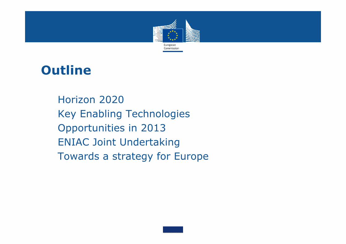
Outline
1. Horizon 20202. Key Enabling Technologies3. Opportunities in 20134. ENIAC Joint Undertaking5. Towards a strategy for Europe
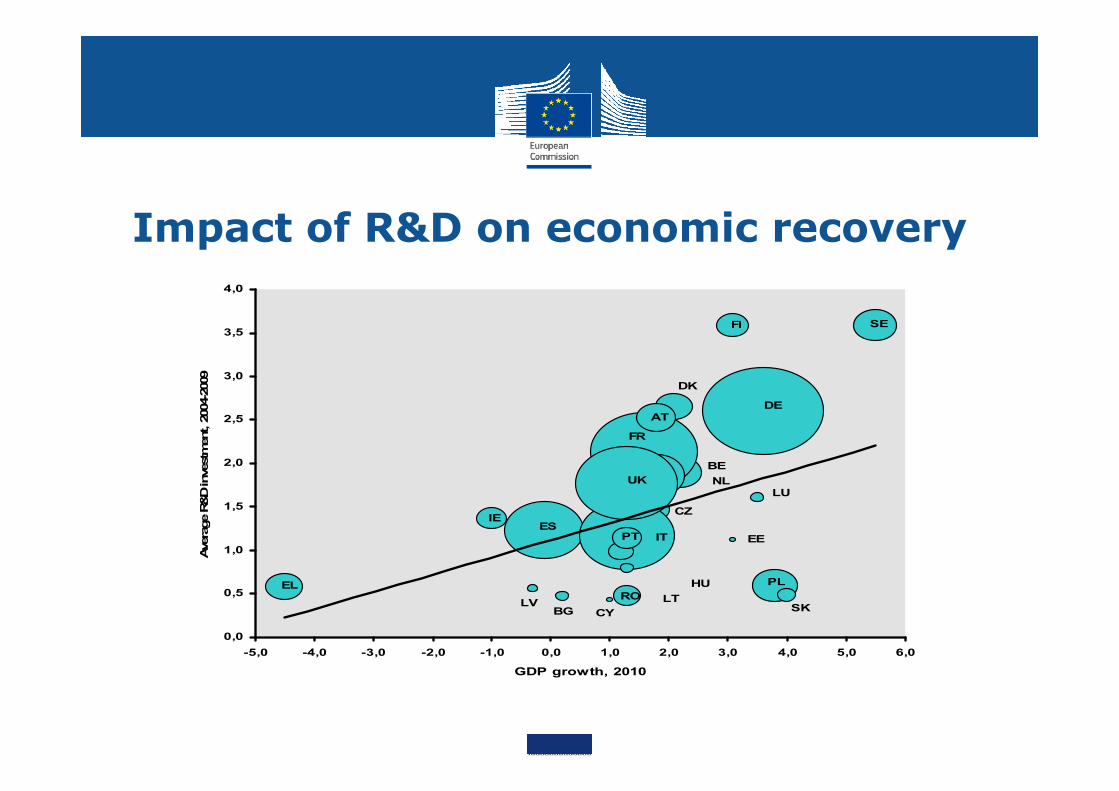
Impact of R&D on economic recovery
NLBE
FR
CZ
UK
DK
AT
EE
DE
LU
PL
SKRO
CY
ES
BGLV
IE
SEFI
ELLT
HU
PT IT
0,0
0,5
1,0
1,5
2,0
2,5
3,0
3,5
4,0
-5,0 -4,0 -3,0 -2,0 -1,0 0,0 1,0 2,0 3,0 4,0 5,0 6,0
GDP growth, 2010
Aver
age
R&D
inve
stm
ent,
2004
-200
9
Outline
1. Horizon 20202. Key Enabling Technologies3. Opportunities in 20134. ENIAC Joint Undertaking5. Towards a strategy for Europe
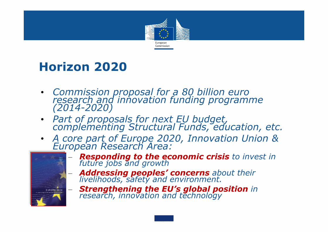
Horizon 2020
• Commission proposal for a 80 billion euro research and innovation funding programme (2014-2020)
• Part of proposals for next EU budget, complementing Structural Funds, education, etc.
• A core part of Europe 2020, Innovation Union & European Research Area:
– Responding to the economic crisis to invest in future jobs and growth
– Addressing peoples’ concerns about their livelihoods, safety and environment.
– Strengthening the EU’s global position in research, innovation and technology
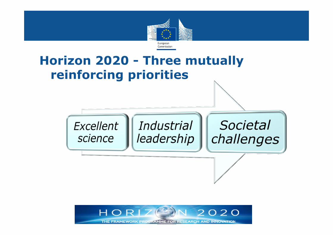
Horizon 2020 - Three mutually reinforcing priorities
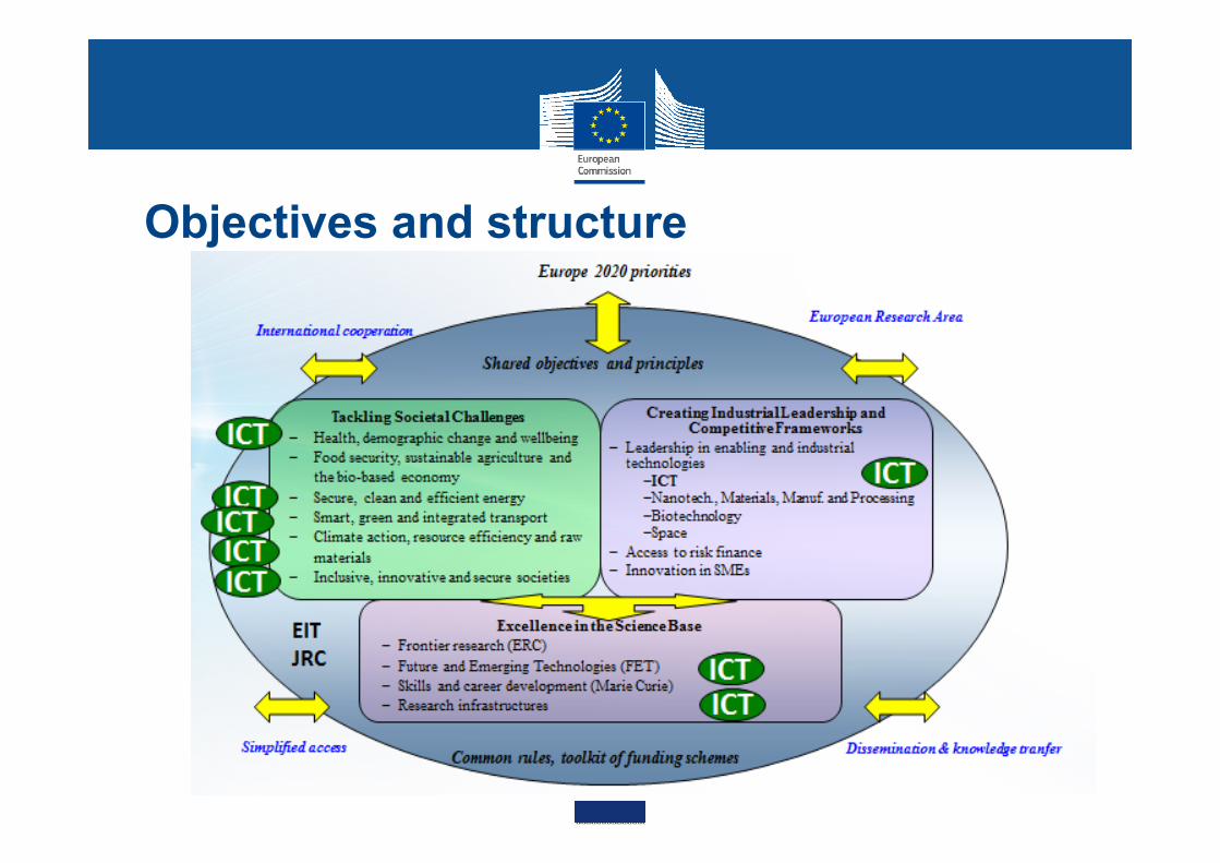
Objectives and structure
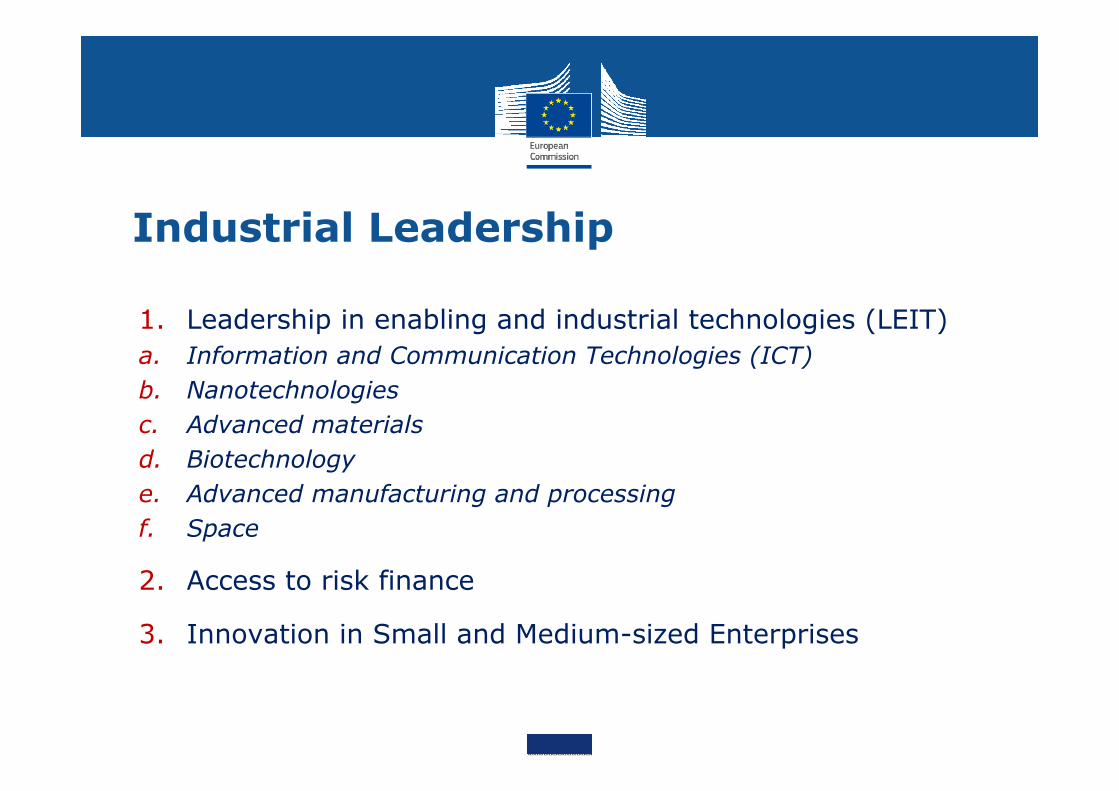
Industrial Leadership
1. Leadership in enabling and industrial technologies (LEIT)a. Information and Communication Technologies (ICT)b. Nanotechnologies c. Advanced materials d. Biotechnologye. Advanced manufacturing and processingf. Space
2. Access to risk finance
3. Innovation in Small and Medium-sized Enterprises
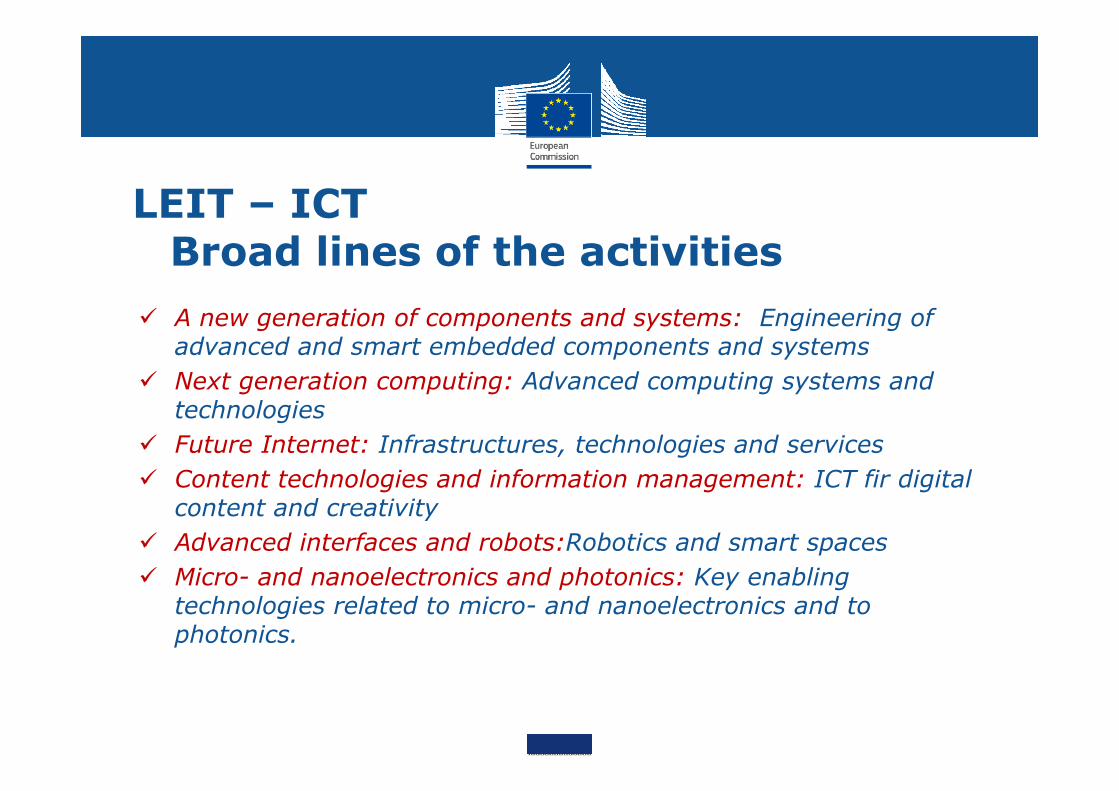
LEIT – ICTBroad lines of the activitiesA new generation of components and systems: Engineering of advanced and smart embedded components and systemsNext generation computing: Advanced computing systems and technologiesFuture Internet: Infrastructures, technologies and servicesContent technologies and information management: ICT fir digital content and creativityAdvanced interfaces and robots:Robotics and smart spacesMicro- and nanoelectronics and photonics: Key enabling technologies related to micro- and nanoelectronics and to photonics.
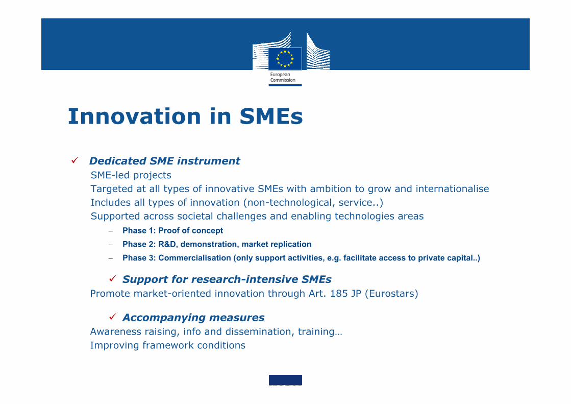
Innovation in SMEs
Dedicated SME instrumentSME-led projectsTargeted at all types of innovative SMEs with ambition to grow and internationaliseIncludes all types of innovation (non-technological, service..)Supported across societal challenges and enabling technologies areas
– Phase 1: Proof of concept– Phase 2: R&D, demonstration, market replication– Phase 3: Commercialisation (only support activities, e.g. facilitate access to private capital..)
Support for research-intensive SMEsPromote market-oriented innovation through Art. 185 JP (Eurostars)
Accompanying measuresAwareness raising, info and dissemination, training…Improving framework conditions
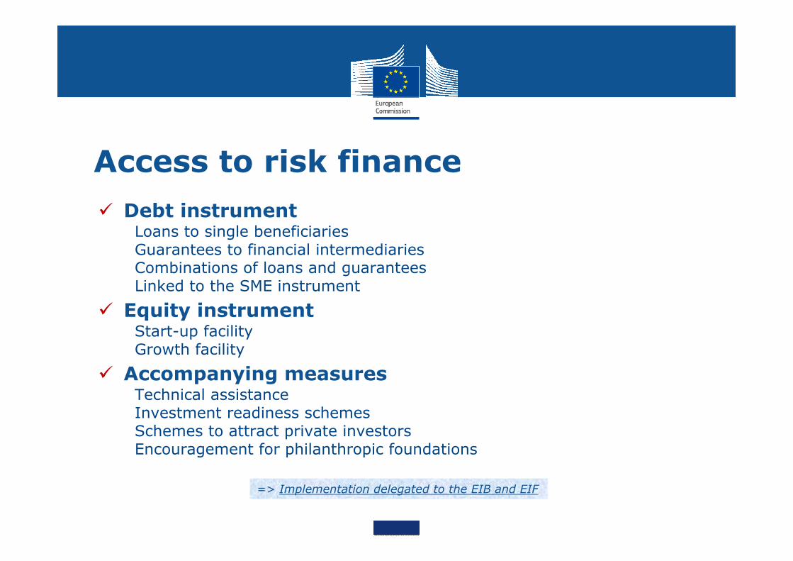
Access to risk financeDebt instrument
Loans to single beneficiariesGuarantees to financial intermediariesCombinations of loans and guaranteesLinked to the SME instrument
Equity instrumentStart-up facilityGrowth facility
Accompanying measuresTechnical assistanceInvestment readiness schemesSchemes to attract private investorsEncouragement for philanthropic foundations
=> Implementation delegated to the EIB and EIF
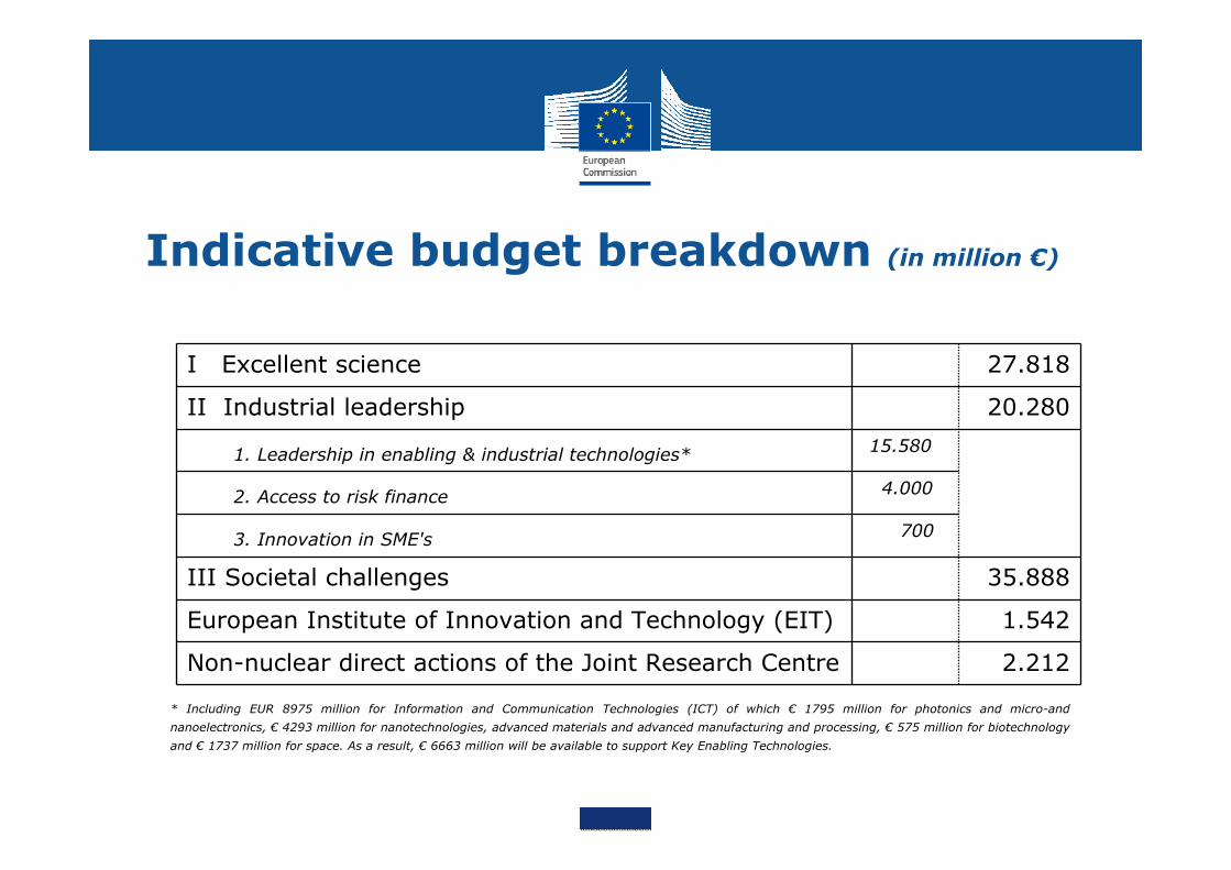
Indicative budget breakdown (in million €)
I Excellent science 27.818
II Industrial leadership 20.280
1. Leadership in enabling & industrial technologies* 15.580
2. Access to risk finance 4.000
3. Innovation in SME's 700
III Societal challenges 35.888
European Institute of Innovation and Technology (EIT) 1.542
Non-nuclear direct actions of the Joint Research Centre 2.212
* Including EUR 8975 million for Information and Communication Technologies (ICT) of which € 1795 million for photonics and micro-and nanoelectronics, € 4293 million for nanotechnologies, advanced materials and advanced manufacturing and processing, € 575 million for biotechnology and € 1737 million for space. As a result, € 6663 million will be available to support Key Enabling Technologies.
Outline
1. Horizon 20202. Key Enabling Technologies3. Opportunities in 20134. ENIAC Joint Undertaking5. Towards a strategy for Europe
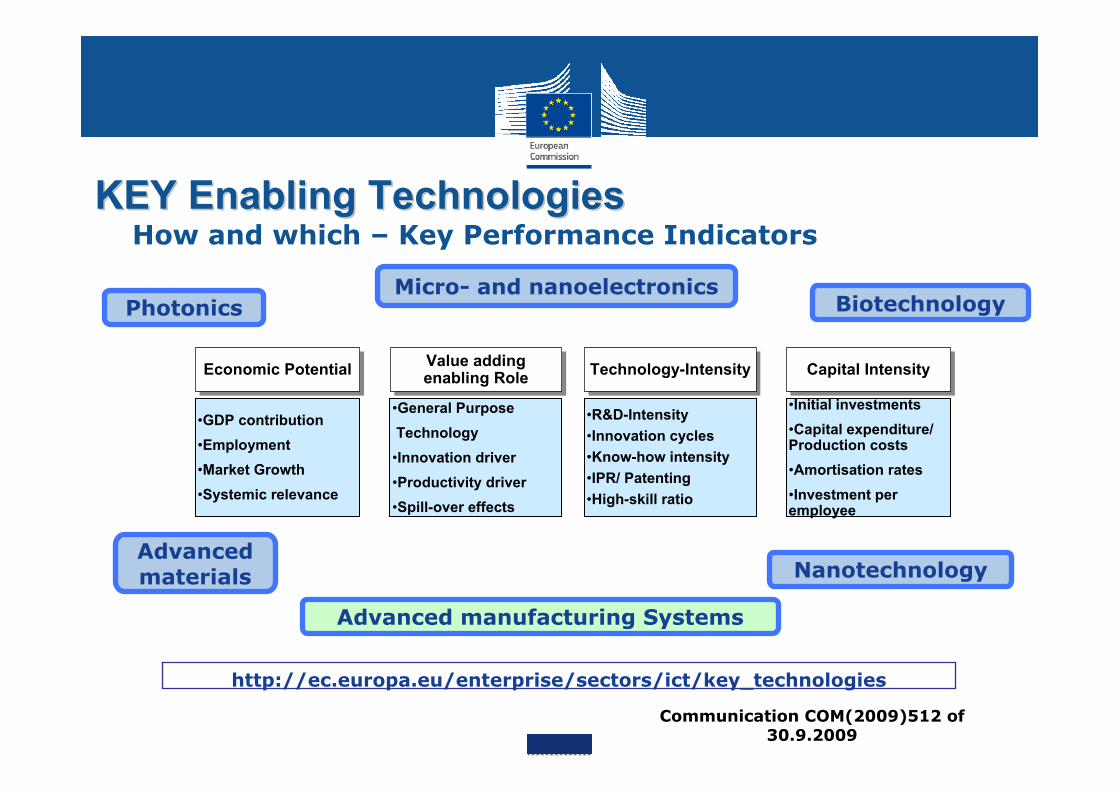
Communication COM(2009)512 of 30.9.2009
http://ec.europa.eu/enterprise/sectors/ict/key_technologies
Nanotechnology
Micro- and nanoelectronicsPhotonics
Advancedmaterials
Biotechnology
Advanced manufacturing Systems
Value adding enabling Role Value adding enabling Role Technology-IntensityTechnology-Intensity Capital Intensity Capital Intensity Economic PotentialEconomic Potential
•Initial investments•Capital expenditure/ Production costs•Amortisation rates•Investment per employee
•GDP contribution•Employment•Market Growth •Systemic relevance
•R&D-Intensity•Innovation cycles•Know-how intensity•IPR/ Patenting•High-skill ratio
•General Purpose Technology
•Innovation driver•Productivity driver•Spill-over effects
KEY Enabling Technologies KEY Enabling Technologies How and which – Key Performance Indicators
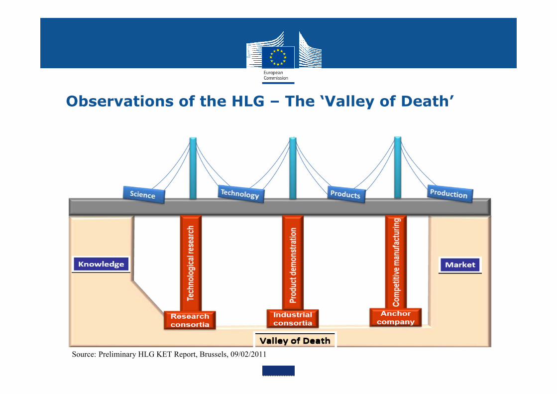
Observations of the HLG – The ‘Valley of Death’
Source: Preliminary HLG KET Report, Brussels, 09/02/2011
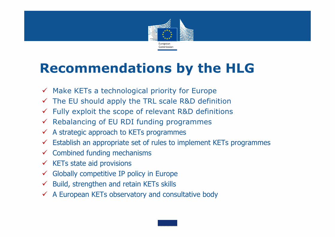
Recommendations by the HLGMake KETs a technological priority for Europe The EU should apply the TRL scale R&D definitionFully exploit the scope of relevant R&D definitionsRebalancing of EU RDI funding programmesA strategic approach to KETs programmesEstablish an appropriate set of rules to implement KETs programmesCombined funding mechanismsKETs state aid provisionsGlobally competitive IP policy in EuropeBuild, strengthen and retain KETs skillsA European KETs observatory and consultative body
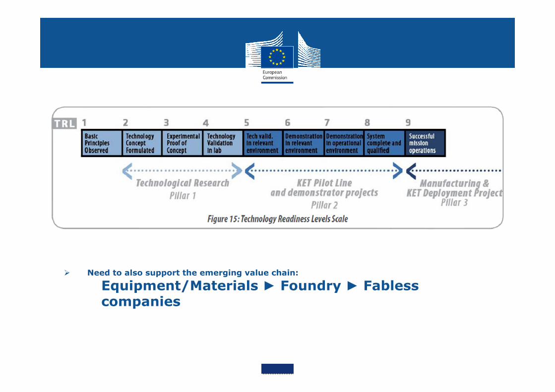
Need to also support the emerging value chain:
Equipment/Materials ► Foundry ► Fabless companies
Outline
1. Horizon 20202. Key Enabling Technologies3. Opportunities in 20134. ENIAC Joint Undertaking5. Towards a strategy for Europe
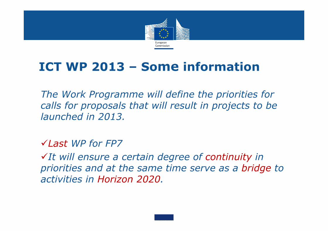
ICT WP 2013 – Some information
The Work Programme will define the priorities for calls for proposals that will result in projects to be launched in 2013.
Last WP for FP7It will ensure a certain degree of continuity in
priorities and at the same time serve as a bridge to activities in Horizon 2020.
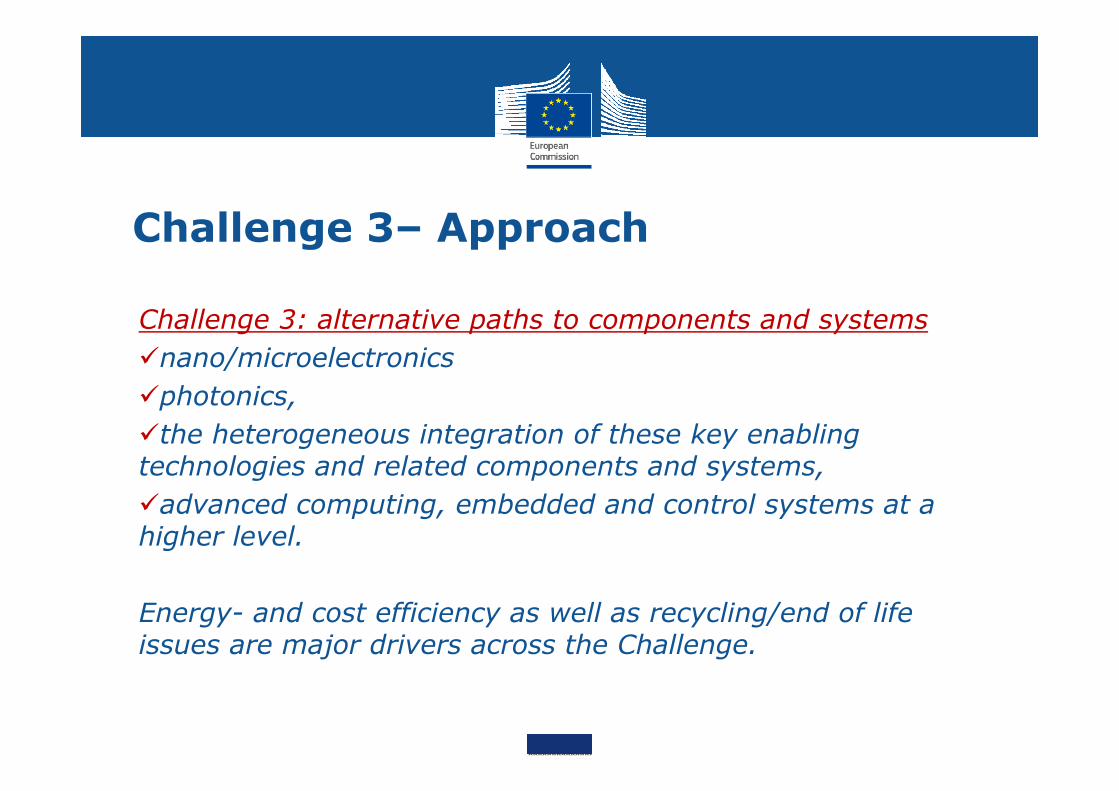
Challenge 3– Approach
Challenge 3: alternative paths to components and systems nano/microelectronicsphotonics, the heterogeneous integration of these key enabling
technologies and related components and systems, advanced computing, embedded and control systems at a
higher level.
Energy- and cost efficiency as well as recycling/end of life issues are major drivers across the Challenge.
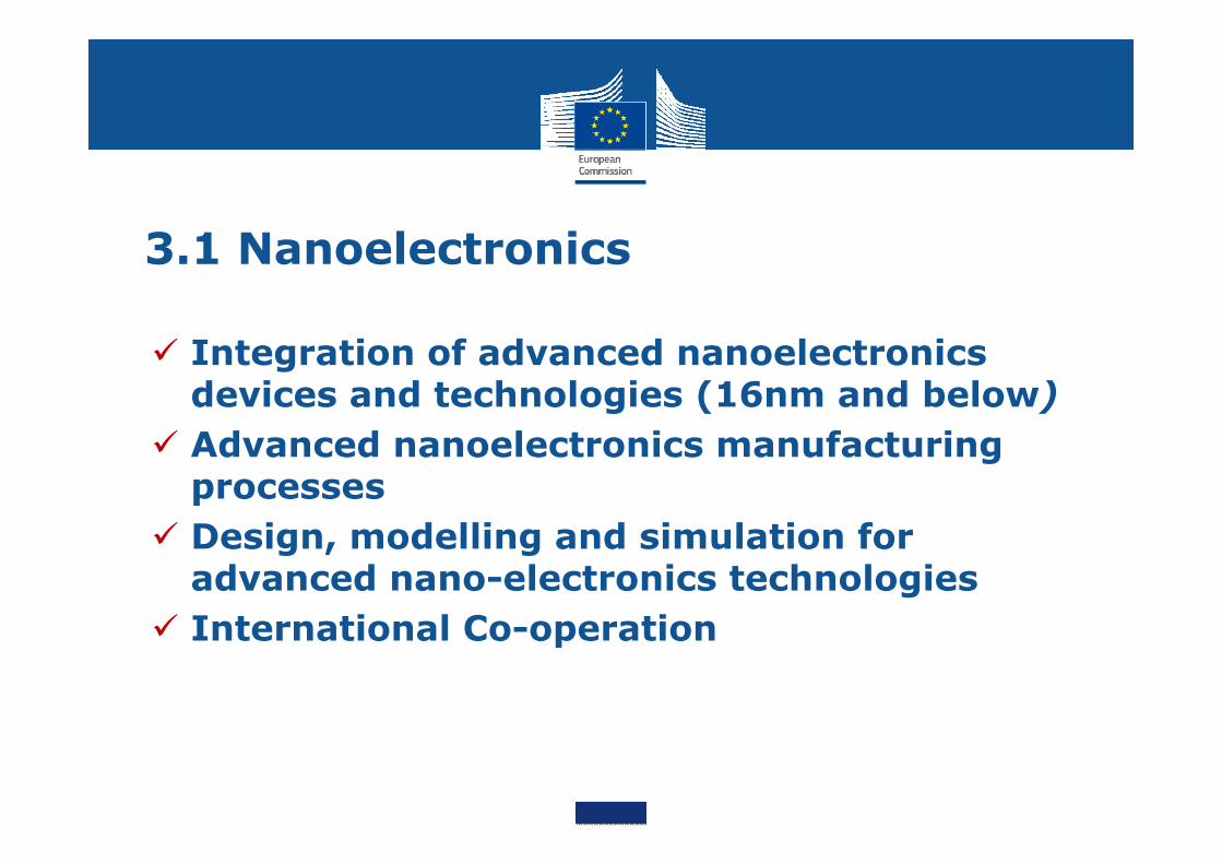
3.1 Nanoelectronics
Integration of advanced nanoelectronics devices and technologies (16nm and below)Advanced nanoelectronics manufacturing processesDesign, modelling and simulation for advanced nano-electronics technologiesInternational Co-operation
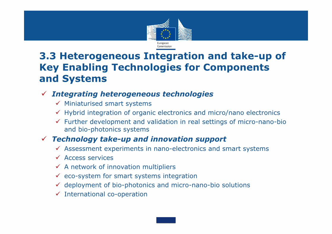
3.3 Heterogeneous Integration and take-up of Key Enabling Technologies for Components and Systems
Integrating heterogeneous technologiesMiniaturised smart systems Hybrid integration of organic electronics and micro/nano electronics Further development and validation in real settings of micro-nano-bio and bio-photonics systems
Technology take-up and innovation supportAssessment experiments in nano-electronics and smart systems Access services A network of innovation multipliers eco-system for smart systems integration deployment of bio-photonics and micro-nano-bio solutionsInternational co-operation
Outline
1. Horizon 20202. Key Enabling Technologies3. Opportunities in 20134. ENIAC Joint Undertaking5. Towards a strategy for Europe
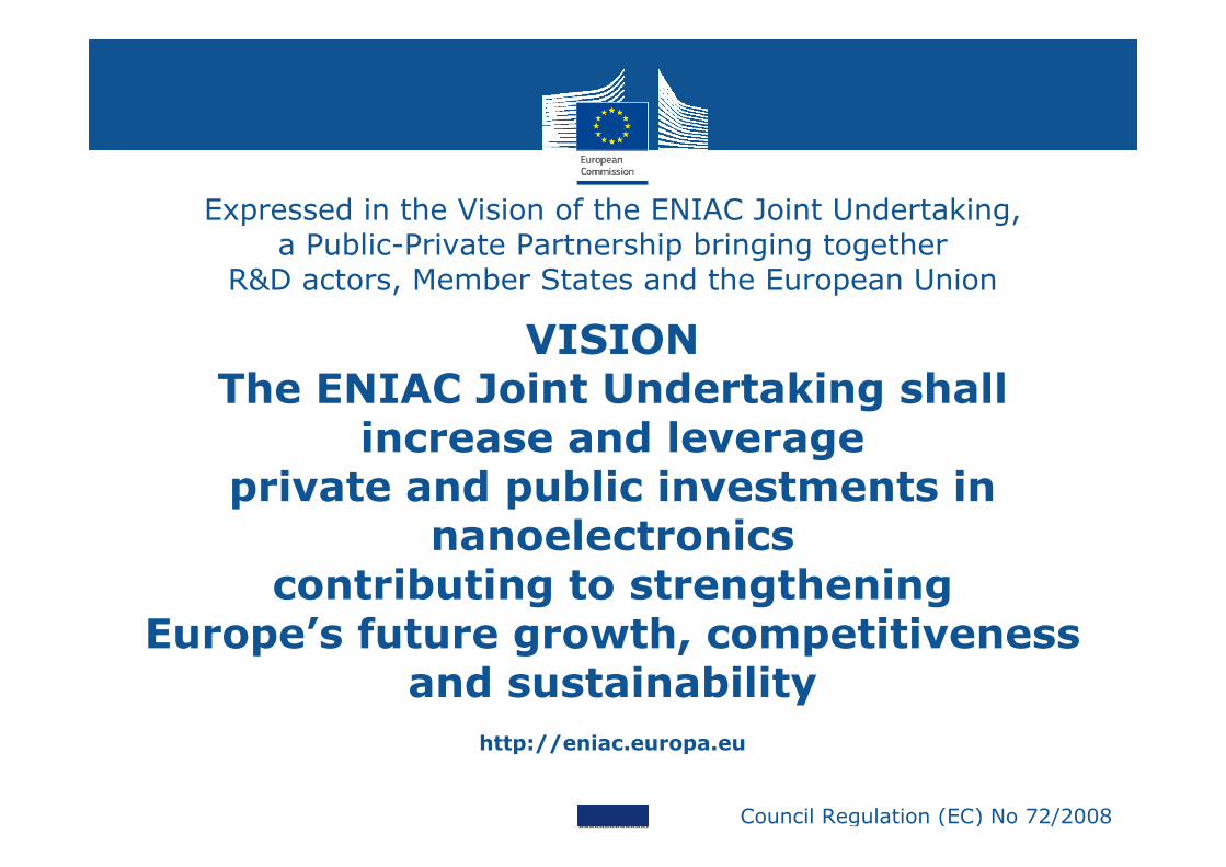
Goal
Expressed in the Vision of the ENIAC Joint Undertaking, a Public-Private Partnership bringing together
R&D actors, Member States and the European Union
VISIONThe ENIAC Joint Undertaking shall
increase and leverage private and public investments in
nanoelectronics contributing to strengthening
Europe’s future growth, competitiveness and sustainability
http://eniac.europa.eu
Council Regulation (EC) No 72/2008
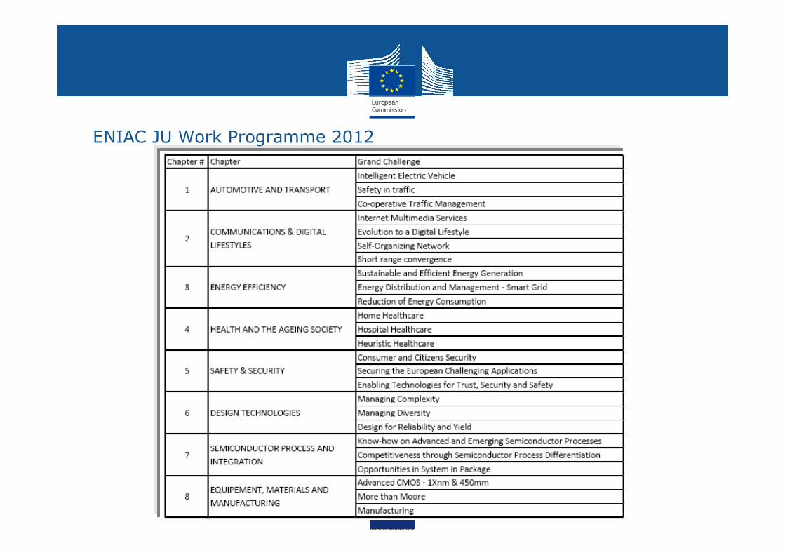
ENIAC JU Work Programme 2012
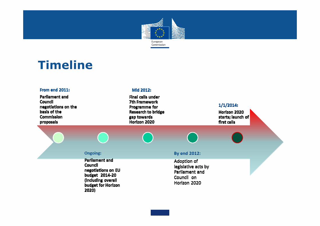
Timeline
Outline
1. Horizon 20202. Key Enabling Technologies3. Opportunities in 20134. ENIAC Joint Undertaking5. Towards a strategy for Europe
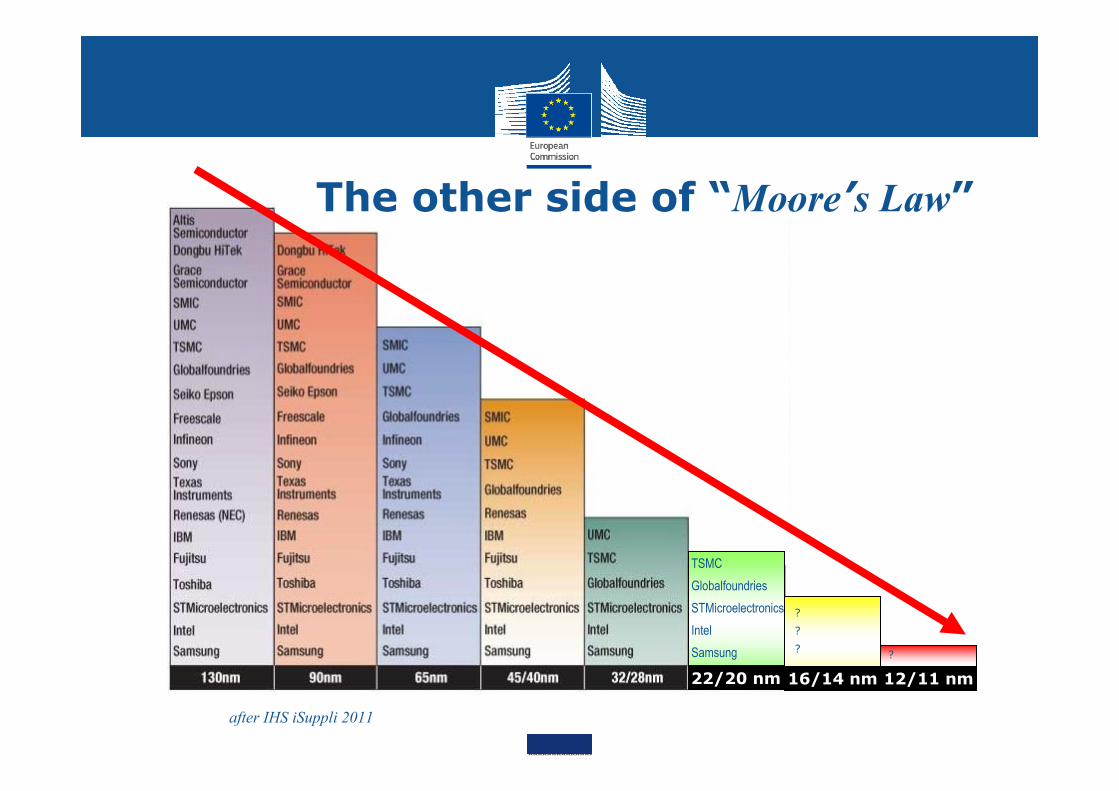
after IHS iSuppli 2011
16/14 nm 12/11 nm
??? ?
TSMCGlobalfoundriesSTMicroelectronicsIntelSamsung
22/20 nm
The other side of “Moore’s Law”
Moo
re’s
Law
: M
inia
turiz
atio
n
Bas
elin
e C
MO
S: C
PU, M
emor
y, L
ogic 130nm
90nm
65nm
45nm
32nm
22nm
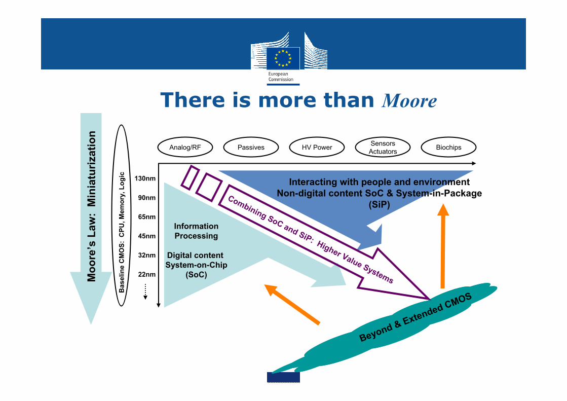
Beyond & Extended CMOS
Analog/RF Passives HV Power SensorsActuators Biochips
InformationProcessing
Digital content System-on-Chip
(SoC)
Interacting with people and environmentNon-digital content SoC & System-in-Package
(SiP)Combining SoC and SiP: Higher Value Systems
There is more than Moore
Neelie Kroes – 24 May 2012:
• "Imagine if we built a whole electronics ecosystem right here. Building on the leading technology institutes, and our world-class equipment and materials industry. Connecting the electronics industry with the markets that demand their innovations — public and private, research and industry, small and large business. And connecting with those who can train and supply skilled labour.
• …• Are we prepared to set strategic alliances, build value
chains in Europe, set R&D priorities and invest further downstream?"
THANK YOU THANK YOU
Information Society and Media: http://ec.europa.eu/information_societyhttp://cordis.europa.eu/fp7/ict/nanoelectronics/mission_en.html
Horizon 2020 on the web: http://ec.europa.eu/research/horizon2020/index_en.cfm