Embed Size (px)
Citation preview

Chemical Vapor Deposition
ESS4810 LectureFall 2010
Introduction
• Chemical vapor deposition (CVD) forms thin films on the surface of a substrate by thermal decomposition and/or reaction of gas compounds
• The desired material is deposited directly from the gas phase onto the surface of the substrate

Advantage
• More conformal deposition– Higher temperature - higher surface
diffusion– Higher pressure – shorter mean free
path
Mechanism
• 1: diffusion of reactants to surface
• 2: absorption of reactants at surface
• 3: chemical reaction at surface
• 4: desorption of gaseous by-products from surface
• 5: diffusion of gaseous by-products from surface

Silicon Deposition
Growth Rate Model
• F1 = flux from bulk of gas to substrate surface
• F2 = flux consumed in film-growth reaction
• F1 = F2
• Film growth rate = F/N– N: atomic density of the deposited film
)(hG SG CC −
SC⋅SkG
G
Ch
⋅+
=s
GS
k
hkF
(unknown)

Boundary Layer Theory
μρδδ
UL
L
3
2(x)dx
L
1 L
0
== ∫
Flow Rate Dependence
rate) flow gas :(U U
Gro
wth
rat
e dy
/dt
Surface reaction limited
Gas transport limited
δG
G
Dh = U∝∝∝
δ1
hdt
dyG

Temperature Dependence
Surface reaction limited
Gas transport limited
kTEs ekk Δ−= 0
kTEeR Δ−∝
3/2TR ∝R
Atmospheric Pressure (APCVD)
Deposition rate is high but uniformity is poor
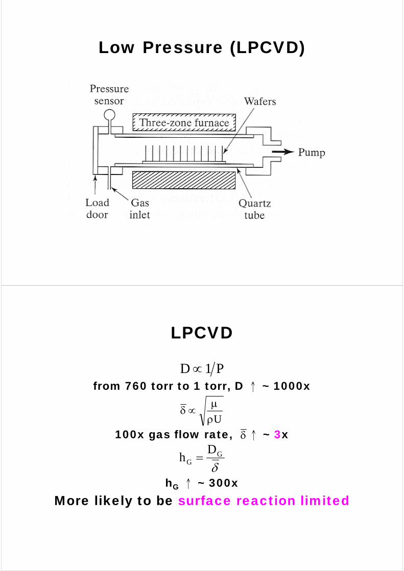
Low Pressure (LPCVD)
LPCVD
from 760 torr to 1 torr, D ↑ ~ 1000x
100x gas flow rate, ↑ ~ 3x
hG ↑ ~ 300xMore likely to be surface reaction limited
P1D ∝
Uρμ
∝δ
δG
G
Dh =
δ

Plasma Enhanced (PECVD)
PECVD• Ionized chemical species allows a lower T to
be used• Film properties (e.g. mechanical stress) can
be tailored by controllable ion bombardment with substrate bias voltage

Polysilicon Deposition
• LPCVD• 600ºC~650ºC• 25~150 Pa• 100% silane or 20%~30% silane diluted
with nitrogen• 100~200 Å/min
24 2HSiSiH +→
• phospho-silicate glass (PSG) [P2O5+SiO2]
300ºC~500ºC
• tetraethylorthosilicate (TEOS)
LPCVD, 650ºC~750ºC
Silicon Dioxide Deposition
2224 2HSiOOSiH +→+
25223 6HO2P5O4PH +→+
byproductsSiO)HSi(OC 2452 +→

APCVD, 700ºC~900ºC
LPCVD, 700ºC~800ºC
• Thermal growth of Si3N4 is possible but not very practical
• 1000ºC~1100ºC• The growth rate is very low
Silicon Nitride Deposition
24334 12HNSi4NH3SiH +→+
243322 6H6HClNSi4NHH3SiCl ++→+
CVD Metal Deposition
• Mo, Ta, and Ti can be deposited in an LPCVD system through reaction with hydrogen
6HFWH3WF 26 +→+
10HCl2M5H2MCl 25 +→+

Reactive Ion Etching
ESS4810 LectureFall 2010
Introduction
• Dry etching: physically/chemically• High-pressure plasma etching• Ion milling• Reactive ion etching• Deep reactive ion etching

High-Pressure Plasma Etching
• High-pressure and low-power• The plasma is used to start and stop the
etching by producing a reactive species from an inert precursor
• Depends primarily on the chemistry
Ion Milling
• Low-pressure and high-power• Pure ion milling or ion-beam etching
involves no chemical reactions• Strictly mechanical process, chemistry
independent• Two significant advantages
– Directionality– Applicability

Ion Milling
Kaufman source Problems
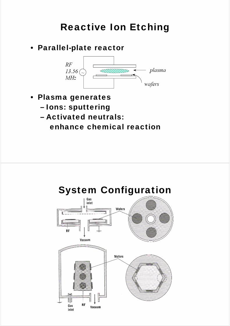
Reactive Ion Etching
• Parallel-plate reactor
• Plasma generates– Ions: sputtering– Activated neutrals:
enhance chemical reaction
System Configuration

Ion-Assisted Etching
• Synergism of ion bombardment + chemical reaction give the high RIE rates
Etching Sequence
Gas flow
Chemical reaction
Diffusion of reactant
Adsorption Desorption
Diffusion of product
Gaseous product
Substrate

Volatility of Etching Product
• Higher vapor pressure usually means higher volatility
• Examplehigh vapor pressurelow vapor pressure
Difficult to RIE Al-Cu alloy with high Cu content

Examples
• Silicon, use CF4 gas
• Aluminum
• Photoresist
Selectivity
• SiO2 etching in CF4+H2 plasmaS = rate of SiO2 / rate of Si
• Reason

Si Etching in CF4+O2 Mixture
(1)F* increases Si etching rate
(2)
(1) (2)(1) (2)
Characteristics

Etching Mechanism
• Removal of surface film and deposition of plasma reaction products can occur simultaneously
Anisotropy
• Ionic bombardment to damage expose surface• Sidewall coating by inhibitor prevents etching

Deep Reactive Ion Etching
Mask
1 μm Mask erosion
ballooning
trenching
product residue
Deep Reactive Ion Etching
• BallooningUse chemistry with a good sidewall inhibitor
• TrenchingUse high pressure to increase ion-neutral scattering (ion trajectory less directional)
• Bottom RoughnessIncrease vapor pressure of etching product

Surface Technology System
Etching Mechanism
• Alternating between etching and protective polymer deposition
• Etching– SF6/Ar + substrate bias
• Polymerization– CHF3/Ar or – C4F8/SF6

HARSE Process
HARSE Process

Local Loading Effect
• Smaller trenches etch at a slower rate than larger trenches

Deep Reactive Ion Etching

ESS4810 Micro System Fabrication and Experiment
Midterm Exam (Fall 2009)
Problem 1 - Clean Room, Wafer Cleaning, and Thermal Oxidation (14%)
(a) Why should a microfabrication clean room be environmentally controlled with respect to (1) airborne particulates and (2) lighting? (3%) Which one of the following two clean rooms has worse control over airborne particulates, class 10 or class 1000? (1%)
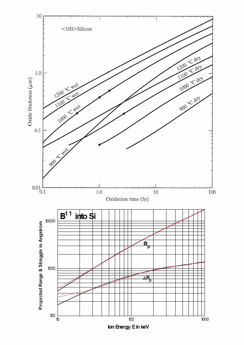
(b) List 2 different ways that are capable of removing residue photoresist. (2%) (c) A bare silicon wafer is oxidized for 3 hours at 1200°C in dry O2. After a series of
lithography and etching steps, SiO2 on half of the wafer is removed. The whole wafer is then re-oxidized at 1000°C in steam. The final oxide thickness in region A is measured to be 0.6 μm. Use the attached oxidation chart to estimate the final oxide thickness in Region B and the step height between A and B. (8%).
Problem 2 - Lithography (20%)
(a) We only measure the overlay errors of the Top and Right alignment marks of a 100 mm diameter wafer.
(i) Calculate the x and y components of the translational error (xt, yt). (3%)
Region A Region B Region A Region B
Si
SiO2 Step height

(ii) Calculate the rotational error (also indicate CW or CCW in the answer). (2%) (iii)Calculate the overlay error of the Left alignment marks. (3%)
(b) An established optical lithography process using G-line illumination (λ=436 nm) can produce a minimum printable feature (=k‧λ/NA) of 0.5 μm with a depth of focus (=λ/2(NA)2) of 1 μm. A new IC product requires a minimum printable feature of 0.2 μm with a depth of focus = 0.15 μm. Two optical steppers are available with the following specifications:
λ NA Stepper A 365 nm (I-line) N1 Stepper B 248 nm (excimer laser) N2
Assuming the technology factor k for minimum printable feature remains the same, what are the ranges of NAs (N1 and N2) that will meet both the minimum printable feature and DOF requirements? (7%)
(c) Describe briefly what the so-called lift-off process is. (3%) (d) Compare positive and negative PRs in terms of resolution and sensitivity. (2%) Problem 3 - Ion Implantation (15%)
Boron implantation is performed to the following structure with a boron dose of 1x10¹⁴/cm2. The B+ ion energy is chosen such that the boron concentration (right after implantation) at location A is a maximum. Assume that the ion stopping powers and ion scattering characteristics are identical for both silicon and silicon dioxide. (a) What is the required B+ ion energy? (3%) (b) The post-implant heat-treatment is 1000°C for 50 minutes with a boron diffusion
constant equal to 1.5×10⁻⁶ µm2/sec. Calculate the boron concentration (after the heat treatment) at location B and A. (7%)
(c) The n-type substrate has a uniform doping concentration of 1x10¹⁵/cm3. Calculate the junction depth underneath location B before and after the heat treatment. (5%)
0.45 μm

Problem 4 – Diffusion (8%)
(a) Explain briefly what thermal budget is. (2%) (b) The following profile B is subjected to an additional drive-in step such that
(Dt)drive-in = 3(Dt)predep. Calculate the surface concentration after drive in. (4%) (c) List 2 major advantages of ion implantation versus dopant diffusion. (2%)
Problem 5 – Vapor Deposition (23%)
(a) A wafer of diameter D is placed at a height H above a small planar evaporation source. Derive an expression for the ratio of the deposited film thickness at location A to that at the center, in terms of x, D, and H. (4%)
(b) If the evaporation source is very far from the wafer, we can treat the evaporation
fluxes to be uniform and parallel. The following contact opening has vertical SiO2 sidewalls and the evaporating flux is making an angle of 20° with respect to the normal of the wafer's surface. If the deposition rate is 1000 Å/min, sketch the cross-sectional profile of the deposited film after 5 min. (7%)
20°

(c) What is the working principle of (1) sputtering (2%) and (2) a cryopump? (2%) (d) List 2 major advantages of using CVD versus PVD for thin film deposition. (3%) (e) Assume a starting substrate profile shown below. A ideal conformal deposition is
then performed with a deposition rate of 0.1 μm/min. Sketch the cross-sections of the deposited film after 1, 2, and 4 minutes of deposition. (5%)
Problem 6 – Etching (21%)
The (100) wafer shown below has nitride masks on its top and bottom surfaces. (1) With KOH, the etch selectivity between the {100} and {111} planes is 400:1 (use
∞:1 in your calculation), and the {100} etch rate is 1.4 μm/min. (2) With TMAH, the etch selectivity between the {100} and {111} planes is 40:1, and
the {100} etch rate is 1.2 μm/min. (3) With HNA, the isotropic etch rate is 1 μm/min. For anisotropic etching, assume that the nitride layers and all other silicon crystal planes are not etched. Sketch the wafer cross sections after 200 minutes of etching (3%) and determine the following dimensions after etching in the all three cases: (a) Silicon etch depth (3%) (b) Silicon etch width at top (6%) (c) Silicon etch width at bottom (3%)
(d) Compare high-pressure plasma and reactive ion etching in terms of their reaction mechanisms. (3%) How to realize ideal high aspect ratio etching? (3%)
500µm
600µm
Silicon nitride Silicon
A A’
A-A’
Top

ESS4810 Micro System Fabrication and Experiment
Midterm Exam (Fall 2008)
Problem 1 - Clean Room, Wafer Cleaning, and Thermal Oxidation (20%)
(a) A microfabrication clean room should be environmentally controlled with respect to airborne particulates and what else? List at least 3 of them. (4.5%) Which one of the following two clean rooms has better control over airborne particulates, class 1 or class 100? (2%)
(b) List at least 2 different ways that is capable of removing residue photoresist. (4%) (c) A bare Si {100} wafer is oxidized for 40 minutes at 900°C in steam. After a series
of lithography and etching steps, SiO2 on half of the wafer is removed. The whole wafer is then re-oxidized in dry O2 at 1100°C. The final oxide thickness in region A is measured to be 0.2 μm. Use the attached oxidation chart to estimate the final oxide thickness in Region B and the step height between Region A and B. (9.5%)
Region A Region B Region A Region B
Si
SiO2 Step height

Problem 2 – Lithography (24%)
(a) We only measure the overlay errors of the Center and Right alignment marks of a 100 mm diameter wafer.
Top Right Center Left Bottom x N/A 3 μm 2 μm x1 N/A y N/A 2 μm 1 μm y1 N/A
(i) Calculate the thermal run in (or out) error. (3%) (ii) Calculate the rotational error (also indicate clockwise or counterclockwise in
your answer). (3%) (iii)Calculate the overlay errors of the Left alignment marks. (3%)
(b) An established optical lithography process using G-line illumination (λ=436 nm) can produce a minimum printable feature (=k‧λ/NA) of 0.5 μm with a Depth of Focus (=λ/2(NA)2) of 1 μm. A new IC product requires a minimum printable feature of 0.2 μm with a Depth of Focus = 0.15 μm. Three optical steppers are available with the following specifications:
λ NA Stepper A 365 nm (I-line) 0.7 Stepper B 248 nm (excimer laser) 0.85 Stepper C 193 nm (ArF) 0.85
Assuming the technology factor k for minimum feature remains the same, which stepper will meet both the minimum feature and DOF requirements? Show calculations to justify your choice. (10%)
(c) Describe briefly what the so-called lift-off process is. (3%) (d) List at least 2 differences between positive and negative photo-resists. (2%)

Problem 3 - Ion Implantation (17%)
Boron implantation is performed to the following structure with a boron dose of 8x10¹³/cm2. The B+ ion energy is chosen such that the boron concentration (right after implantation) at location B is a maximum. Assume that the ion stopping powers and ion scattering characteristics are identical for both silicon and silicon dioxide. (a) What is the required B+ ion energy? (3%) (b) The post-implant heat-treatment is 1000°C for 40 minutes with a boron diffusion
constant equal to 1.8×10⁻⁶ µm2/sec. Calculate the boron concentration (after the heat treatment) at location B and A. (10%)
(c) The n-type silicon substrate has a uniform doping concentration of 1x10¹⁵/cm3. Calculate the junction depth xj underneath location A. (4%)
0.45

Problem 4 – Diffusion (8%)
(a) Explain briefly what thermal budget is. (3%) (b) A boron pre-deposition step is performed into an n-type Si substrate at 1000°C.
The solid solubility of boron in silicon is known to be 3.5× 10²⁰/cm3 at 1000°C and the incorporated boron dose Q is 1 ×10¹⁵/cm2. What is the junction depth xj of the pre-deposition profile if the n-type substrate has a background concentration of 1015/cm3? (5%)
Problem 5 – Physical Vapor Depostion (19%)
(a) If the evaporation source is very far from the wafer, we can treat the evaporation fluxes to be uniform and parallel. The following contact opening has vertical SiO2 sidewalls and the evaporating flux is making an angle of 35° with respect to the normal of the wafer's surface. If the deposition rate is 1200 Å/min, sketch the cross-sectional profile of the deposited film after 5 min. (5%)
(b) A Si wafer of 10 cm diameter with a tilting angle (φ) of 5° is placed at a height of
30 cm above a planar evaporation source. Calculate the ratio of the deposited thickness at the center to that at the edge of the wafer. (7%)
(c) What is the working principle of sputtering? (3%) What are the advantages of
sputtering over evaporation? (2%) (d) Which one of the following two pumps can achieve higher vacuum, diaphragm
pump or turbomolecular pump? (2%)
35°

Problem 6 – Etching (18%)
The silicon (100) wafer shown below has patterned silicon nitride masks on its top and bottom surfaces. (1) With KOH, the etch selectivity between the {100} and {111} planes is 400:1 (use
∞:1 in your calculation), and the {100} etch rate is 1.4 μm/min. (2) With TMAH, the etch selectivity between the {100} and {111} planes is 40:1, and
the {100} etch rate is 1.2 μm/min. Assuming that the silicon nitride layers and all other silicon crystal planes are not etched, sketch the wafer cross sections after 300 minutes of etching (3%) and determine the following dimensions after etching in both KOH and TMAH cases: (a) Silicon etching depth (2%) (b) Silicon etch width at top (5%) (c) Silicon etch width at bottom (4%) (d) In case there is an elliptic opening B on the top nitride mask, what will be the final
shape of the cavity after 300 minutes of KOH etching? (Sketch both the top and cross-sectional views.) (4%)
500µm
600µm
Silicon nitride Silicon
A A’
A-A’
Top
B
100 μm
100 μm

ESS4810 Micro System Fabrication and Experiment
Midterm Exam (Fall 2007)
Problem 1 - Clean Room, Wafer Cleaning, and Thermal Oxidation (20%)
(a) List at least 3 basic requirements for a microfabrication clean room. (3%) Which one of the following two clean rooms has better control over airborne particulates, class 1 or class 100? (1.5%)
(b) List at least 3 major functions of SiO2 in microfabrication. (2.5%) (c) List at least 2 advantages of wet wafer cleaning over dry wafer cleaning. (2%) (d) A bare Si {100} wafer is oxidized for 40 minutes at 900°C in steam. After a series
of lithography and etching steps, SiO2 on half of the wafer is removed. The whole wafer is then re-oxidized in dry O2 at 1100°C. The final oxide thickness in region A is measured to be 0.2 μm. Use the attached oxidation chart to estimate the final oxide thickness in Region B and the step height between Region A and B. (11%)
Region A Region B Region A Region B
Si
SiO2 Step height

Problem 2 – Lithography (24%)
(a) We only measure the overlay errors of the Center and Right alignment marks of a 100 mm diameter wafer.
Top Right Center Left Bottom x N/A 3 μm 2 μm x1 x2 y N/A 2 μm 1 μm y1 y2
(i) Calculate the thermal run in (or out) error. (3%) (ii) Calculate the rotational error (also indicate clockwise or counterclockwise in
your answer). (3%) (iii)Calculate the overlay errors of the Left and Bottom alignment marks. (6%)
(b) For projection lithography, the printable resolution R equals to kλ/(NA) and the depth of focus DOF equals to λ/2(NA)2. The k-factor is known as the technology factor since it depends on both diffraction and resist effects. Suppose we improve on the resist technology such that k is reduced by 25%. For fixed λ and R, calculate the percentage of change in DOF. (3%)
(c) What is the typical procedure of a photo-lithography process? (3%) (d) List at least 2 differences between positive and negative photo-resists. (2%) (e) Describe briefly what the so-called lift-off process is. (4%)

Problem 3 - Ion Implantation (17%)
Boron implantation is performed to the following structure with a boron dose of 5x10¹³/cm2. The B+ ion energy is chosen such that the boron concentration at location B is a maximum. For simplicity, let us assume the ion stopping powers and ion scattering characteristics are identical for both silicon and silicon dioxide. (a) What is the required B+ ion energy? (3%) (b) The post-implant heat-treatment is 1000°C for 30 minutes with a boron diffusion
constant equal to 1.6×10⁻⁶ µm2/sec. Calculate the boron concentration at location B and A. (10%)
(c) The n-type silicon substrate has a uniform doping concentration of 2x10¹⁵/cm3. Calculate the junction depth xj underneath location A. (4%)
0.45

Problem 4 – Diffusion (9%)
(a) Describe briefly the two-step diffusion process. (2%) List 2 disadvantages of diffusion over ion implantation (2%)
(b) A boron pre-deposition step is performed into an n-type Si substrate at 1000°C. The solid solubility of boron in silicon is known to be 3.5× 10²⁰/cm3 at 1000°C and the incorporated boron dose Q is 2 ×10¹⁵/cm2. What is the junction depth xj of the pre-deposition profile if the n-type substrate has a background concentration of 1015/cm3? (5%)
Problem 5 – Evaporation (20%)
(a) If the evaporation source is very far from the wafer, we can treat the evaporation fluxes to be uniform and parallel. The following contact opening has vertical SiO2 sidewalls and the evaporating flux is making an angle of 40° with respect to the normal of the wafer's surface. If the deposition rate is 1000 Å/min, sketch the cross-sectional profile of the deposited film after 5 min. (5%)
(b) A Si wafer of 10 cm diameter with a tilting angle (φ) of 10° is placed at a height
of 30 cm above a planar evaporation source. Calculate the ratio of the deposited thickness at the center to that at the edge of the wafer. (7%)
(c) What are the working principles of evaporation and sputtering? (4%) Why must
these processes be operated under vacuum? (2%) (d) List 2 methods for high vacuum measurement. (2%)
40°

Problem 6 – Etching (20%)
The silicon (100) wafer shown below has patterned silicon nitride masks on its top and bottom surfaces. (1) With KOH, the etch selectivity between the {100} and {111} planes is 400:1 (use
∞:1 in your calculation), and the {100} etch rate is 1.5 μm/min. (2) With TMAH, the etch selectivity between the {100} and {111} planes is 30:1, and
the {100} etch rate is 1.2 μm/min. Assuming that the silicon nitride layers and all other silicon crystal planes are not etched, sketch the wafer cross sections after 250 minutes of etching (4%) and determine the following dimensions after etching in both KOH and TMAH cases: (a) Silicon etching depth (2%) (b) Silicon etch width at top (5%) (c) Silicon etch width at bottom (5%) (d) In case there is an elliptic opening B on the top nitride mask, what will be the final
shape of the cavity after 300 minutes of KOH etching? (Sketch both the top and cross-sectional views.) (4%)
500µm
700µm
Silicon nitride Silicon
A A’
A-A’
Top
B
100 μm
100 μm

ESS4810 Micro System Fabrication and Experiment
Midterm Exam (Fall 2006)
Problem 1 - Clean Room, Wafer Cleaning, and Thermal Oxidation (18%)
(a) What are the requirements for a microfabrication clean room? (3%) For what purposes? (2%)
(b) What are the major functions of SiO2 in micro system fabrication? (3%) (c) List 2 methods for wafer cleaning. (2%) (d) A bare Si (100) wafer is oxidized for 3 hours at 1200°C in dry O2. After a
lithographic and etching step SiO2 on half of the wafer is removed. The whole wafer is then re-oxidized in steam at 1000°C. The final oxide thickness in region A is measured to be 1 μm. Use the oxidation chart to estimate the oxide thickness in Region B. (8%)
Region A Region B Region A Region B
Si
SiO2

Problem 2 – Lithography (17%)
(a) We only measure the overlay errors for the Right and Top alignment marks near the edge of a 100 mm diameter wafer.
(i) Calculate the x and y components of the translational error (xt, yt). (5%) (ii) Calculate the thermal run in / run out error. (3%) (iii)Calculate the rotational error (also indicate clockwise or counterclockwise in
your answer). (3%) (b) What is the typical procedure of a photo-lithography process? (3%) (c) What are the differences between positive and negative photo-resists? (3%)
Problem 3 - Ion Implantation (19%)
Boron implantation is performed to the following structure with a boron dose of 2.5x10¹³/cm2. The B+ ion energy is chosen such that the boron concentration at location B is a maximum. For simplicity, let us assume the ion stopping powers and ion scattering characteristics are identical for both silicon and silicon dioxide. (a) What is the B+ ion energy? (3%) (b) Calculate the boron concentration at location B and A. (8%) (c) The n-type silicon substrate has a uniform doping concentration of 2x10¹⁵/cm3.
Calculate the junction depth xj underneath location A. (4%) (d) What are the advantages of ion implantation over diffusion? (4%)
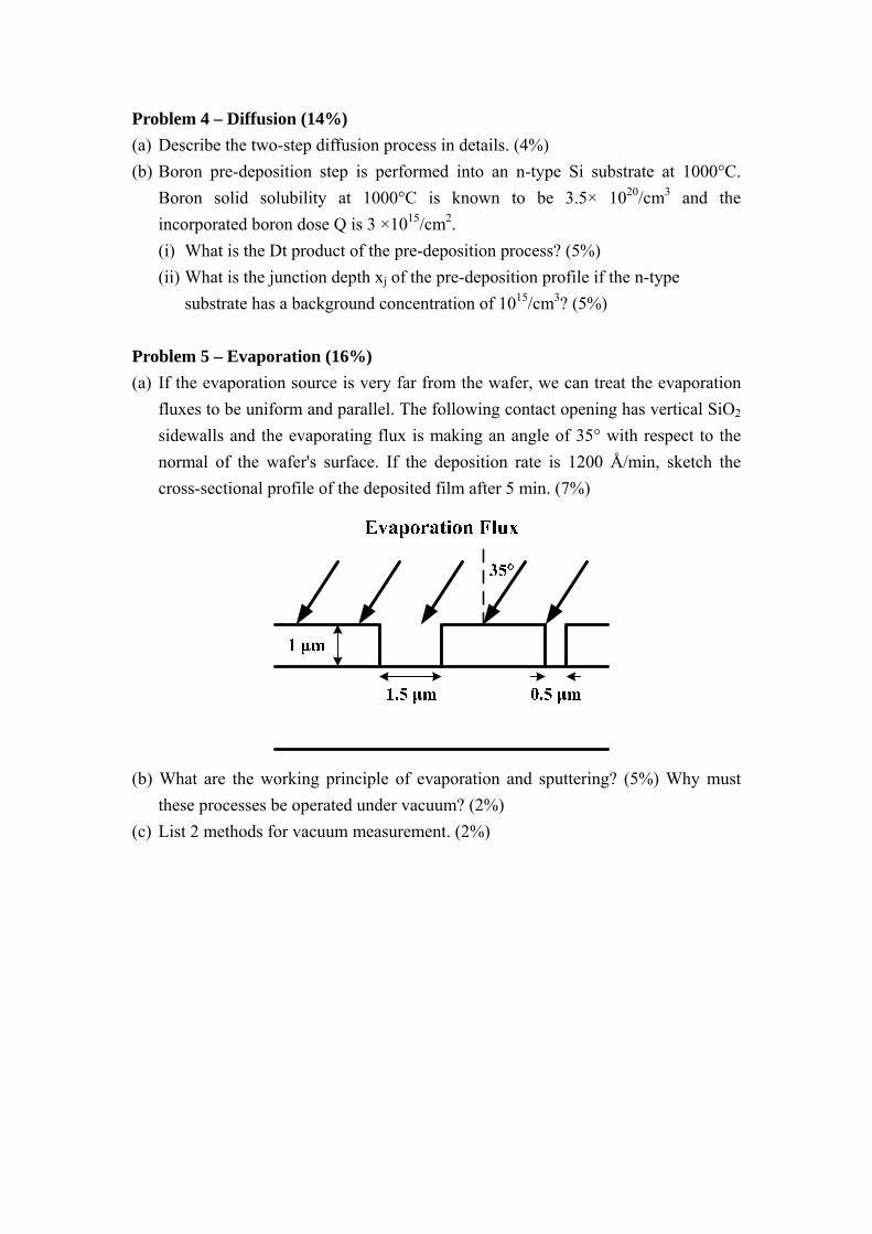
Problem 4 – Diffusion (14%)
(a) Describe the two-step diffusion process in details. (4%) (b) Boron pre-deposition step is performed into an n-type Si substrate at 1000°C.
Boron solid solubility at 1000°C is known to be 3.5× 10²⁰/cm3 and the incorporated boron dose Q is 3 ×10¹⁵/cm2.
(i) What is the Dt product of the pre-deposition process? (5%) (ii) What is the junction depth xj of the pre-deposition profile if the n-type
substrate has a background concentration of 1015/cm3? (5%) Problem 5 – Evaporation (16%)
(a) If the evaporation source is very far from the wafer, we can treat the evaporation fluxes to be uniform and parallel. The following contact opening has vertical SiO2 sidewalls and the evaporating flux is making an angle of 35° with respect to the normal of the wafer's surface. If the deposition rate is 1200 Å/min, sketch the cross-sectional profile of the deposited film after 5 min. (7%)
(b) What are the working principle of evaporation and sputtering? (5%) Why must these processes be operated under vacuum? (2%)
(c) List 2 methods for vacuum measurement. (2%)

Problem 6 – Etching (16%)
The silicon {100} wafer shown below has patterned silicon nitride masks on both top and bottom surfaces. (1) With KOH, the etch selectivity between the {100} and {111} planes is 400:1 (use
∞:1 in your calculation), and the {100} etch rate is 1.4 μm/min. (2) With TMAH, the etch selectivity between the {100} and {111} planes is 40:1, and
the {100} etch rate is 1.1 μm/min. Assuming that the silicon nitride layer and all other silicon crystal planes are not etched, sketch the wafer cross section after 300 minutes of etching (3%) and determine the following dimensions after etching in both KOH and TMAH cases: (a) Silicon etching depth (2%) (b) Silicon etch width at top (4%) (c) Silicon etch width at bottom (4%) (d) In case there is an elliptic opening B on the nitride mask, what will be the final
shape of the cavity after 300 minutes of KOH etching? (3%)
500µm
700µm
Silicon nitride Silicon
A A’
A-A’
Top
B
100 μm