Embed Size (px)
Citation preview

I
ENHANCED SMMITTM FAMILYProduct Handbook
Aeroflex Colorado Springs, Inc.4350 Centennial Blvd.
Colorado Springs, CO 80907
October 12, 2015

Table of Contents
1.0 INTRODUCTION 11.1 Remote Terminal Features 1 1.1.1 Indexing 1 1.1.2 Buffer Ping-Pong 1 1.1.3 Circular Buffers 1 1.1.4 Internal Illegalization 1 1.1.5 Broadcast 1 1.1.6 Interrupt History 1 1.1.7 Message Information 11.2 Bus Controller Features 1 1.2.1 Multiple Message Processing 2 1.2.2 Message Scheduling 2 1.2.3 Polling 2 1.2.4 Automatic Retry 21.3 Monitor Terminal Features 2 1.3.1 Message Information 21.4 Remote Terminal/Monitor Terminal Features 21.5 Protocol Definition 21.6 SMMIT Transceivers 21.7 SMMIT XTE Memory 2
2.0 REMOTE TERMINAL ARCHITECTURE 62.1 Register Descriptions 6
2.1.1 Control Register 62.1.2 Operational Status Register 82.1.3 Current Command Register 92.1.4 Interrupt Mask Register 102.1.5 Pending Interrupt Register 102.1.6 Interrupt Log List Pointer Register 122.1.7 Bit Word Register 122.1.8 Time-Tag Register 132.1.9 Remote Terminal Descriptor Pointer Register 132.1.10 1553 Status Word Bits Register 142.1.11 Illegalization Registers 16
2.2 Descriptor Block 182.2.1 Receive Control Word 212.2.2 Transmit Control Word 222.2.3 Mode Code Receive Control Word 232.2.4 Mode Code Transmit Control Word 242.2.5 Data Pointer A and B 252.2.6 Broadcast Data Pointer 25
2.3 Data Structures 252.3.1 Subaddress Receive Data 282.3.2 Subaddress Transmit Data 28
II

III
2.3.2.1 Transmit Information (Info) Word 292.3.3 Mode Code Data 29
2.3.3.1 Mode Code Receive Information (Info) Word 302.3.3.2 Mode Code Transmit Information (Info) Word 30
2.4 Mode Code and Subaddress 312.5 Encoder and Decoder 332.6 RT-RT Transfer Compare 332.7 Terminal Address 332.8 Reset 332.9 MIL-STD-1553A Operation 34
3.0 BUS CONTROLLER ARCHITECTURE 353.1 Register Descriptions 35
3.1.1 Control Register 363.1.2 Operational Status Register 373.1.3 Current Command Register 383.1.4 Interrupt Mask Register 383.1.5 Pending Interrupt Register 393.1.6 Interrupt Log List Pointer Register 403.1.7 BIT Word Register 403.1.8 Minor Frame Timer Register 403.1.9 Command Block Pointer Register 413.1.10 BC Command Block Initialization Control Register 41
3.2 SBC Architecture 423.2.1 Control Word 43
3.2.1.1 Opcode Definition 443.2.1.2 Condition Codes 45
3.2.2 Command Words 453.2.3 Data Pointer 453.2.4 Status Words 463.2.5 Branch Address 463.2.6 Timer Value 46
3.3 Command Block Chaining 463.4 Memory Architecture 483.5 Message Processing 493.6 MIL-STD-1553A Operation 50
4.0 MONITOR TERMINAL ARCHITECTURE 514.1 Register Descriptions 51
4.1.1 Control Register 524.1.2 Operational Status Register 534.1.3 Current Command Register 544.1.4 Interrupt Mask Register 544.1.5 Pending Interrupt Register 554.1.6 Interrupt Log List Pointer Register 554.1.7 BIT Word Register 564.1.8 Time-Tag Register 564.1.9 Initial Monitor Block Pointer Register 56

4.1.10 Initial Monitor Data Pointer Register 574.1.11 Monitor Block Counter Register 574.1.12 Monitor Filter Register 574.1.13 Monitor Filter Register 57
4.2 SMT Architecture 584.2.1 Message Information Word 58
4.2.1.1 Message Information Bits 594.2.2 Command Words 594.2.3 Data Pointer 594.2.4 Status Words 594.2.5 Time-Tag 594.2.6 Unused 59
4.3 Monitor Block Chaining 604.4 Memory Architecture 604.5 Message Processing 61
4.5.1 Error Condition Message Processing 614.6 Remote Terminal/Monitor Terminal Operation 614.7 MIL-STD-1553A Operation 62
5.0 ENHANCED SMMIT FAMILY OPERATION 635.1 Message Time-out 635.2 DMA Time-out 635.3 Circular Buffers 63
5.3.1 Mode Number 0 635.3.2 Mode Number 1 635.3.3 Mode Number 2 64
5.4 Ping-Pong Handshake 645.5 Circular Buffer #1 645.6 Circular Buffer #2 665.7 Ping-Pong Enable/Disable Handshake 68
6.0 INTERRUPT ARCHITECTURE 716.1 SMMIT E & SMMIT LXE/DXE 71
6.1.1 Interrupt Identification Word (IIW) 716.1.2 Interrupt Address Word (IAW) 716.1.3 Interrupt Log List Address 71
6.2 SMMIT XTE 746.2.1 Interrupt Identification Word (IIW) 746.2.2 Interrupt Address Word (IAW) 746.2.3 Interrupt Log List Address 74
7.0 AUTO-INITIALIZATION 767.1 SMMIT E & SMMIT LXE/DXE 76
7.1.1 SRT Auto-Initialization 767.1.2 SMT Auto-Initialization 767.1.3 SBC Auto-Initialization 767.1.4 Auto-Initialization Hardware 76
7.2 SMMIT XTE 78
IV
V
7.2.1 SRT Auto-Initialization 787.2.2 SMT Auto-Initialization 787.2.3 SBC Auto-Initialization 787.2.4 Auto-Initialization Hardware 78
8.0 TESTABILITY 81
9.0 SYSTEM CONFIGURATION 829.1 SMMIT E & SMMIT LXE/DXE 82
9.1.1 Transmitter/Receiver Interface 829.1.2 Register Transfers 839.1.3 DMA Configuration 849.1.4 DMA Transfers 849.1.5 Buffer Mode Operation 84
9.2 SMMIT XTE 879.2.1 Internal Registers 879.2.2 Memory Map 879.2.3 Buffer Mode Operation 879.2.4 Hardware Interface 87
10.0 SERIAL DATA BUS INTERFACE 9410.1 Transmitter 9410.2 Receiver 9410.3 Recommended Thermal Protection 94
11.0 SMMIT PIN IDENTIFICATION AND DESCRIPTION 9711.1 SMMIT Functional Pin Description 98
11.1.1 Data Bus 9811.1.2 Address Bus 9911.1.3 Remote Terminal Address Inputs 9911.1.4 JTAG Testability Pins 10011.1.5 Biphase Inputs 10011.1.6 Biphase Outputs 10111.1.7 DMA Signals 10111.1.8 Control Signals 10311.1.9 Status Signals 10311.1.10 Power/Ground 104
12.0 SMMIT LX/DX PIN IDENTIFICATION AND DESCRIPTION 10512.1 SMMIT Functional Pin Description 106
12.1.1 Data Bus 10612.1.2 Address Bus 10712.1.3 Remote Terminal Address Inputs 10712.1.4 JTAG Testability Pins 10812.1.5 Biphase Inputs/Outputs 10812.1.6 DMA Signals 10912.1.7 Control Signals 110
VI
12.1.8 Status Signals 11112.1.9 Power/Ground 112
13.0 SMMIT XT PIN IDENTIFICATION AND DESCRIPTION 11313.1 SMMIT Functional Pin Description 114
13.1.1 Data Bus DA 11413.1.2 Address Bus A(15:0) 11513.1.3 Auto-initialization Address Bus EA(12:0) 11513.1.4 Auto-initialization Data Bus ED(7:0) 11613.1.5 Remote Terminal Address Inputs 11613.1.6 JTAG Testability Pins 11713.1.7 Biphase Inputs/Outputs 11713.1.8 Control Signals 11813.1.9 Status Signals 12013.1.10 Power/Ground 12013.1.11 No Comments 121
14.0 SMMIT E ABSOLUTE MAXIMUM RATINGS 122
15.0 SMMIT E RECOMMENDED OPERATING CONDITIONS 122
16.0 SMMIT E DC ELECTRICAL CHARACTERISTICS 123
17.0 SMMIT LXE/DXE & SMMIT XTE ABSOLUTE MAXIMUM 124 RATINGS
18.0 SMMIT LXE/DXE & SMMIT XTE RECOMMENDED OPERATING CONDITIONS 125
19.0 SMMIXT LXE/DXE & SMMIT XTE DC ELECTRICALCHARACTERISTICS 12619.1 SMMIT DXE & XTE DC Electrical Characteristics 12619.2 SMMIT LXE & XTE (15 & 12) DC Electrical Characteristics 12719.3 SMMIT DXE & XTE (5) DC Electrical Characteristics 127
20.0 SMMIT E & SMMIT LXE/DXE AC ELECTRICALCHARACTERISTICS 128
21.0 SMMIT XTE AC ELECTRICAL CHARACTERISTICS 135
22.0 SMMIT LXE/DXE & SMMIT XTE RECEIVER ELECTRICALCHARACTERISTICS 14622.1 SMMIT LXE & XTE (15 & 12) Receiver Electrical Characteristics 14622.2 SMMIT DXE & XTE (5) Receiver Electrical Characteristics 147

23.0 SMMIT LXE/DXE & SMMIT XTE TRANSMITTERELECTRICAL CHARACTERISTICS 14823.1 SMMIT LXE & XTE (15 & 12) Transmitter Electrical
Characteristics 14823.2 SMMIT DXE & XTE (5) Transmitter Electrical Characteristics 149
24.0 SMMIT LXE/DXE & SMMIT XTE AC ELECTRICAL CHARACTERISTICS 15024.1 SMMIT LXE & XTE (15 & 12) AC Electrical Characteristics 15024.2 SMMIT DXE & XTE (5) AC Electrical Characteristics 150
25.0 PACKAGING 153
26.0 ORDERING INFORMATION 160
APPENDIX 1 - UT63M1XX MIL-STD-1553A/B TRANSCEIVERAPPENDIX 2 - UT63M14X MIL-STD-1553A/B TRANSCEIVERAPPENDIX 3 - UT54ACTS220 - CLOCK AND WAIT-STATE CIRCUITAPPENDIX 4 - Step-by-Step Guide to 1553 Design Application Note
VII

The SMMITTM FAMILY
VIII
SµMMIT FAMILY - 1
1.0 INTRODUCTION
The monolithic SµMMIT provides the system designer with an intelligent solution to MIL-STD-1553 multiplexed serial data bus design problems. The SµMMIT is a single-chip device that implements all three of the defined MIL-STD-1553 functions - Remote Terminal, Bus Controller, and Monitor. Operating either autonomously or with a tightly coupled host, the SµMMIT will solve a wide range of MIL-STD-1553 interface problems. A powerful RISC processing unit provides automatic message handling, message status, general status, and interrupt information. The register-based interface architecture provides many programmable functions as well as extensive information pertinent to device maintenance. In either of the three operating modes, the SµMMIT can access up to 64K x 16 of external memory (65,536 x 16).
The SµMMIT (which derives its name from serial, µ−coded, monolithic, multi-mode, intelligent, terminal) is a powerful asset to a system designer solving the MIL-STD-1553 problem.
1.1 Remote Terminal FeaturesThe SµMMIT Remote Terminal (SRT) conforms to the requirements of MIL-STD-1553B, Notice II. In addition to meeting the requirements of the standard, the SRT has an extensive list of flexible features to meet any MIL-STD-1553 interface requirement.
1.1.1 IndexingThe SRT can buffer up to 256 receive messages on a subaddress-by-subaddress basis. Upon reception of the specified number of messages, the SRT can generate an interrupt by signaling either the host or subsystem that data is ready for processing. The indexing feature is commonly used to implement bulk data transfer algorithms.
1.1.2 Buffer Ping-PongTo support the transfer of periodic data, double buffering schemes are often incorporated into remote terminal designs. Periodic data transfer incorporates the use of two data buffers per subaddress. The remote terminal processes messages (receive or transmit) via the designated primary buffer. The host or subsystem uses the secondary buffer to collect new data for transmission or processing data received during the defined time interval. Upon completion of the defined interval, the remote terminal will switch the primary and secondary data buffers (i.e., ping-pong). The SRT supports ping-pong buffering via a user-selected ping-pong architecture consisting of dual subaddress data pointers.
1.1.3 Circular Buffers SµMMIT circular buffer modes simplify the software service of remote terminals implementing bulk or periodic data transfers. The SµMMIT architecture allows the user to select one of two circular buffer modes. The user selects the preferred mode, at start-up, by writing to Control Register bits.
1.1.4 Internal IllegalizationAn internal 256-bit (16 x 16) RAM allows for the illegalization of all mode codes and subaddresses. The illegalization RAM is accessed at the beginning of message processing to determine if the valid command is prohibited. To eliminate host or subsystem overhead, the SµΜΜIT can initialize the 256-bit illegalization RAM during the auto-initialization sequence.
1.1.5 BroadcastDesigned to meet the requirements of MIL-STD-1553B Notice II, the SRT can store all data associated with a broadcast command in separate memory from non-broadcast commands. This feature is user-selected via the Descriptor Control word and internal Control Register.
1.1.6 Interrupt HistoryA programmable interrupt structure allows the host or subsystem the flexibility to enter 16 interrupts into a 32-word buffer before service. This feature allows the logging of multiple interrupts if immediate service is restricted. The interrupt structure enters an Interrupt Information Word (IIW) and an Interrupt Address Word (IAW) indicating what subaddress or command block generated the interrupt. All modes of operation support interrupt logging.
1.1.7 Message InformationThe SRT generates a Message Information Word and time-tag (16-bit) for all transacted messages. This information is written into memory along with message data words. The Message Information Word contains word count, message errors, and message type information.
1.2 Bus Controller FeaturesThe SµMMIT Bus Controller (SBC) is a powerful MIL-STD-1553 bus controller developed to meet the requirements of multi-frame processing with low host overhead. User-defined decision making allows the SBC to operate autonomously from the host until a designated event or series of events has taken place.

SµMMIT FAMILY - 2
1.2.1 Multiple Message ProcessingThe SBC architecture allows the chaining of multiple MIL-STD-1553 commands into major and minor frames depending on the application. This feature allows the host to structure message frames that perform independent tasks such as periodic data transfer, service requests, and bus diagnostics (initiate BIT). The SBC uses a simple opcode scheme to control the command block flow.
1.2.2 Message SchedulingThe SBC allows host entry of data to control the time between messages. This feature is useful when the BC has to perform periodic message transactions with multiple remote terminals.
1.2.3 PollingThe host instructs the SBC to interrogate the status word response of remote terminals to determine if any SBC action is required. The SBC can detect the assertion of status word bits and generate interrupts or branch to a new message frame. Polling is useful if the application requires control of message frame flow as a function of remote terminal response.
1.2.4 Automatic RetryThe SBC can automatically retry a message on busy, message error, or other status word bit response. If enabled, the SBC can retry up to four times, per command block, on the primary bus or alternate bus.
1.3 Monitor Terminal FeaturesThe SµMMIT Monitor Terminal (SMT) is a full-featured MIL-STD-1553B bus monitor designed to monitor all or selected remote terminals on the bus. Requiring little host intervention, the SMT will monitor selected remote terminals until a pre-defined message count is reached. Generation of an interrupt alerts the host that SMT service is required.
1.3.1 Message InformationEach message transaction generates a Message Information Word. This information helps determine message validity and remote terminal health. The Message Information Word is stored in external memory along with message data words.
1.4 Remote Terminal/Monitor Terminal FeatureFor those applications that require the SMT to transfer or receive information, the SµMMIT is configured as both a remote terminal (SRT) and monitor (SMT). This feature allows the SMT to communicate on the bus as a RT, and monitor bus activity. Configuration as both SMT and SRT precludes the SMT from monitoring its own remote terminal address.
1.5 Protocol DefinitionFor maximum flexibility, the SµΜΜIT has been designed to operate in many different systems which use various protocols. Specifically, two of the protocols that the SµMMIT may interface are MIL-STD-1553A and MIL-STD-1553B. To meet these protocols, the SµΜΜIT may be configured through an external pin or through control register bits.
1.6 SµMMIT LXE/DXE & XTE Transceivers Internal monolithic transceivers are complete transmitter and receiver pairs for MIL-STD-1553A and 1553B applications. The receiver section accepts biphase-modulated Manchester II bipolar data from MIL-STD-1553 data bus and produces TTL-level signal data at its internal RXOUT and RXOUT outputs.
The transmitter section accepts biphase TTL-level signal data at its internal TXIN and TXIN inputs and produces MIL-STD-1553 data signals. The transmitter’s output voltage is typically 10VP-P,LL for the SµMMIT XTE5 & DXE and 42VP-P,LL for
the SµMMIT XTE15, XTE12 & LXE.
1.7 SµMMIT XTE MemoryThe SµMMIT XTE contains 512 Kbits of internal memory for message processing. Internal logic generates a RDY signal for the subsystem interface. The internal memory is memory mapped.

SµMMIT FAMILY - 3
SµMMIT FEATURES
r Comprehensive MIL-STD-1553 dual redundant Bus Controller (BC), Remote Terminal (RT), and Monitor Terminal (MT)
r MIL-STD-1553B, Notice II RT- Internal command illegalization in the RT mode- 16-bit read/write time-tag with user-defined resolution- Subaddress data buffering
r Simultaneous RT/MT mode of operation
r Flexible BC architecture designed to off-load the host computer - Minor frame timing- Efficient command block flow statements (Branch, Go To, Call)- Status word polling- Programmable retries
r Programmable interrupt architecture with automatic interrupt logging available in all modes
r Autonomous operation in all three modes of operation- Ideal for low cost remote terminals
r Built-In Test capability
r Supports IEEE Standard 1149.1 (JTAG)
r Radiation-hardened option available
r Flexible packaging offering: - 84-pin pingrid array (PGA)- 84-lead flatpack- 132-lead flatpack
r Standard Microcircuit Drawing 5962-92118 available- QML Q & V compliant
Figure 1. UT69151 SµMMIT Block Diagram
DECODER
DECODER
CLOCK andRESET LOGIC
BUILT-IN TEST
DATA TRANSFER
LOGIC
INTERRUPT CONTROL
INSTRUCTION MEMORY
BOUNDARYSCAN
CONTROL
MASTER RESET AND
CLOCKS
ADDRESS/DATAAND
CONTROL SIGNALS
INTERRUPT OUTPUTS
CONFIGURATIONCONTROL INPUTS
STATUSSIGNALS
ENCODER
BC CONTROLLERRT CONTROLLERMT CONTROLLER
REGISTER FILE(32 x 16)
MESSAGE BUFFER
OU
TP
UT
MU
LTIP
LE
XO
R A
ND
SE
LF
-TE
ST
WR
AP
-AR
OU
ND
LO
GIC
CHANNEL A
CHANNEL B
SµMMIT FAMILY - 4
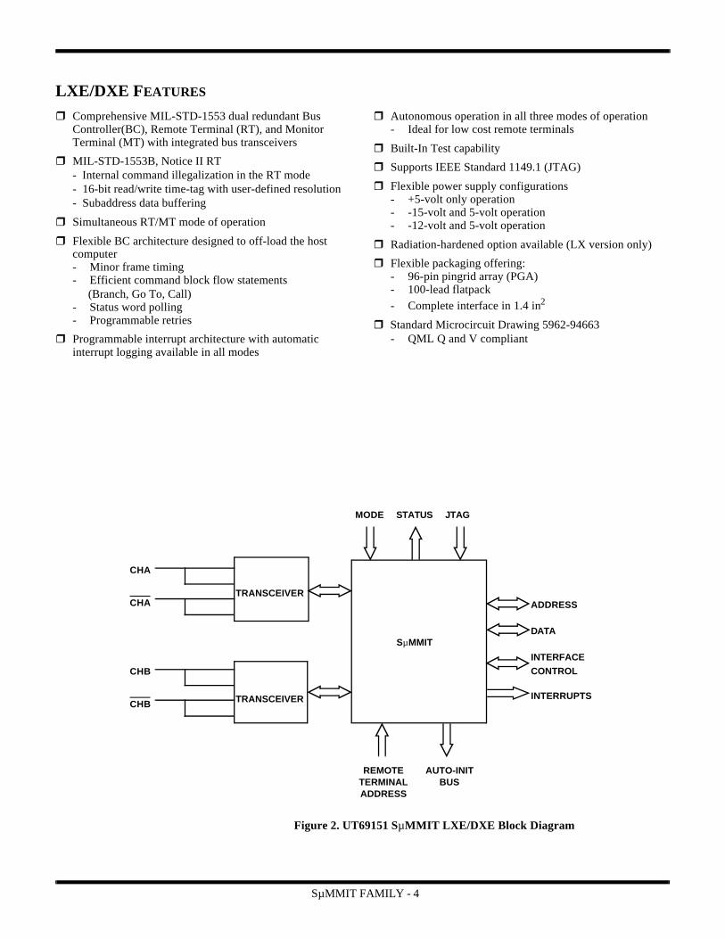
LXE/DXE FEATURES
r Comprehensive MIL-STD-1553 dual redundant Bus Controller(BC), Remote Terminal (RT), and Monitor Terminal (MT) with integrated bus transceivers
r MIL-STD-1553B, Notice II RT- Internal command illegalization in the RT mode- 16-bit read/write time-tag with user-defined resolution- Subaddress data buffering
r Simultaneous RT/MT mode of operation
r Flexible BC architecture designed to off-load the host computer - Minor frame timing- Efficient command block flow statements
(Branch, Go To, Call)- Status word polling- Programmable retries
r Programmable interrupt architecture with automatic interrupt logging available in all modes
r Autonomous operation in all three modes of operation- Ideal for low cost remote terminals
r Built-In Test capability
r Supports IEEE Standard 1149.1 (JTAG)
r Flexible power supply configurations- +5-volt only operation- -15-volt and 5-volt operation- -12-volt and 5-volt operation
r Radiation-hardened option available (LX version only)
r Flexible packaging offering:- 96-pin pingrid array (PGA)- 100-lead flatpack- Complete interface in 1.4 in2
r Standard Microcircuit Drawing 5962-94663 - QML Q and V compliant
TRANSCEIVER
CHA
CHA
TRANSCEIVER
CHB
CHB
SµMMIT
REMOTETERMINALADDRESS
AUTO-INITBUS
MODE STATUS JTAG
ADDRESS
DATA
INTERFACE
CONTROL
Figure 2. UT69151 SµMMIT LXE/DXE Block Diagram
INTERRUPTS
SµMMIT FAMILY - 5
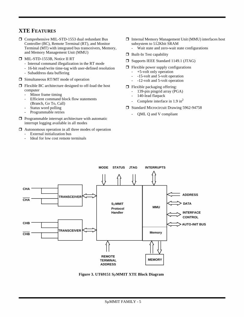
XTE FEATURES
r Comprehensive MIL-STD-1553 dual redundant Bus Controller (BC), Remote Terminal (RT), and Monitor Terminal (MT) with integrated bus transceivers, Memory, and Memory Management Unit (MMU)
r MIL-STD-1553B, Notice II RT- Internal command illegalization in the RT mode- 16-bit read/write time-tag with user-defined resolution- Subaddress data buffering
r Simultaneous RT/MT mode of operation
r Flexible BC architecture designed to off-load the host computer - Minor frame timing- Efficient command block flow statements (Branch, Go To, Call)- Status word polling- Programmable retries
r Programmable interrupt architecture with automatic interrupt logging available in all modes
r Autonomous operation in all three modes of operation- External initialization bus- Ideal for low cost remote terminals
r Internal Memory Management Unit (MMU) interfaces host subsystem to 512Kbit SRAM- Wait state and zero-wait state configurations
r Built-In Test capability
r Supports IEEE Standard 1149.1 (JTAG)
r Flexible power supply configurations- +5-volt only operation- -15-volt and 5-volt operation- -12-volt and 5-volt operation
r Flexible packaging offering:- 139-pin pingrid array (PGA)- 140-lead flatpack- Complete interface in 1.9 in2
r Standard Microcircuit Drawing 5962-94758
- QML Q and V compliant
TRANSCEIVER
CHA
CHA
TRANSCEIVER
CHB
CHB
SµMMIT
Protocol Handler
MMU
ADDRESS
DATA
INTERFACE
CONTROL
REMOTETERMINALADDRESS
MEMORY
MODE STATUS INTERRUPTSJTAG
Figure 3. UT69151 SµMMIT XTE Block Diagram
Memory
AUTO-INIT BUS

SμMMIT FAMILY - 6
2.0 REMOTE TERMINAL ARCHITECTURE
The SμMMIT Remote Terminal (SRT) is an interface device linking a MIL-STD-1553 serial data bus to a host microprocessor and/or subsystem. The SRT’s MIL-STD-1553 interface includes encoding/decoding logic, error detection, command recognition, DMA interface, control/configuration registers, clock, and reset logic. The following sections review
the architecture and use. Each section supplies information on the SRT’s configuration and operation.
2.1 Register DescriptionsThe following list provides the bit descriptions of the 32 internal registers that control SRT operation. All register bits are active high and reflect a logic zero condition (0000 hex) after Master Reset (except those reflecting input pins).
Note: Reference section 9.1.2 for SμMMIT XTE 8-bit register address numbers.
2.1.1 Control Register (Read/Write) - Register 0This 16-bit register controls SRT configuration. To make changes to the SRT and this register, the STEX bit (Bit 15 of the Control Register) must be logic zero. Note: The user has 5μs after TERACT active to stop execution.
Register Number
Name Register Address
0 Control Register 0000 (hex)1 Operational Status Register 0001 (hex)2 Current Command Register 0002 (hex)3 Interrupt Mask Register 0003 (hex)4 Pending Interrupt Register 0004 (hex)5 Interrupt Log List Pointer Register 0005 (hex)6 BIT Word Register 0006 (hex)7 Time-Tag Register 0007 (hex)8 SRT Descriptor Pointer Register 0008 (hex)9 1553 Status Word Bits Register 0009 (hex)10-15 Not Applicable 000A to 000F (hex)16-31 Illegalization Registers 0010 to 001F (hex)
Bit Mnemonic DescriptionNumber
15 STEX Start Execution. Assertion of this bit initiates SμΜΜIT operation. A Control Register write negating this bit inhibits SμΜΜIT operation. A remote terminal address parity error prevents SRT operation regardless of the logical state of this bit. If a RT address parity error exists, bit 3 of Register 1 will be set low and bit 2 of Register 1 will be set high.
14 SBIT Start BIT. Assertion of this bit places the SμΜΜIT into the Built-In Test routine. The BIT test has a fault coverage of 93.4%. If the SμΜΜIT has been started, the host must halt the device in order to place the SμΜΜIT into the Built-In Test routine (STEX = 0) (see section 8.0 for additional information).Note: If Start BIT (SBIT) and Start Execution (STEX) are both set on one register write, BIT has priority.

SμMMIT FAMILY - 7
13 SRST Software Reset. Assertion of this bit immediately places the SμΜΜIT into a software reset. The software reset (which takes 5μs to execute), like MRST, clears all internal logic. Note: During auto-initialization this bit should not be loaded with a logic one. SRST will only function after READYB is asserted.
12 CHAEN Channel A Enable. Setting this bit enables Channel A operation. If negated, the SRT does not recognize commands received over Channel A.
11 CHBEN Channel B Enable. Setting this bit enables Channel B operation. If negated, the SRT does not recognize commands received over Channel B.
10 ETCE External Timer Clock Enable. Assertion of this bit to a logic one allows the external timer clock input to supply stimulus to the internal time-tag counter. Refer to section 2.1.8 for additional information.Note: The user can only change the clock frequency before starting the device (i.e., setting bit 15 of Register 0 to a logic one).
9-7 -- See section 5, Enhanced SμMMIT Family Operation for additional information.
6 BUFR Buffer Mode Enable. Assertion of this bit enables the buffer mode of operation. For more detailed information on this feature refer to sections 9.1.5 or 9.2.3.
5 N/A Not Applicable.
4 BCEN Broadcast Enable. Assertion of this bit enables the SRT broadcast option. Negation of this bit enables remote terminal address 31 as a unique remote terminal address.
3 DYNBC Dynamic Bus Control Acceptance. This bit controls the SRT’s ability to accept the dynamic bus control mode code. Assertion of this bit allows the SRT to respond to a dynamic bus control mode code with status word bit 18 set to a logic one. Negation of this bit prevents the assertion of status word bit 18 upon reception of the dynamic mode code.
2 PPEN Ping-Pong Enable. Assertion of this bit enables the ping-pong buffer feature of the SRT and disables the message indexing feature. Negation of this bit disables the ping-pong feature and enables the message indexing feature. See section 5, Enhanced SμMMIT Family Operation for additional information.
1 INTEN Interrupt Log Enable. Assertion of this bit enables the SμΜΜIT interrupt logging feature. Negation of this bit prevents the logging of interrupts.
0 XMTSW Transmit Status Word. Assertion of this bit allows the SRT to automatically execute the TRANSMIT STATUS WORD mode code when configured for MIL-STD-1553A mode operation. Refer to section 2.9 for additional information.
Bit Mnemonic DescriptionNumberBit Mnemonic DescriptionNumber

SμMMIT FAMILY - 8
2.1.2 Operational Status Register (Read/Write) - Register 1This register reflects pertinent status information for the SRT and is not reset to 0000 (hex) on MRST. Instead, the register reflects the actual stimulus applied to input pins RTA(4:0), RTPTY, MSEL(1:0), A/B STD, and LOCK. Assertion of the LOCK input prevents the modification of the remote terminal address, mode selects, and A or B Standard. In this case, a write to this register’s most significant nine bits is meaningless. If LOCK is negated, a read of this register reflects the information written into this register’s most significant nine bits.
Note: To make changes to the SRT and this register, the STEX bit (Bit 15 in Register 0) must be logic zero.Bit Mnemonic DescriptionNumber
15 RTA4 Terminal Address Bit 4. This bit is the most significant bit of the remote terminal address. This bit is latched on the rising edge of MRST and is a read only bit if the LOCK pin is active.
14 RTA3 Terminal Address Bit 3. This bit is Bit 3 of the remote terminal address. This bit is latched on the rising edge of MRST and is a read only bit if the LOCK pin is active.
13 RTA2 Terminal Address Bit 2. This bit is Bit 2 of the remote terminal address. This bit is latched on the rising edge of MRST and is a read only bit if the LOCK pin is active.
12 RTA1 Terminal Address Bit 1. This bit is Bit 1 of the remote terminal address. This bit is latched on the rising edge of MRST and is a read only bit if the LOCK pin is active.
11 RTA0 Terminal Address Bit 0. This bit is the least significant bit of the remote terminal address. This bit is latched on the rising edge of MRST and is a read only bit if the LOCK pin is active.
10 RTPTY Terminal Address Parity Bit. This bit is appended to the remote terminal address bus (RTA(4:0)) to supply odd parity. The SRT requires odd parity for proper operation. This bit is latched on the rising edge of MRST and is a read only bit if the LOCK pin is active.
9 MSEL(1) Mode Select 1. In conjunction with MSEL0, this bit determines the SμΜΜIT mode of operation. This bit is latched on the rising edge of MRST and is a read only bit if the LOCK pin is active.
8 MSEL(0) Mode Select 0. In conjunction with MSEL1, this bit determines the SμΜΜIT mode of operation. This bit is latched on the rising edge of MRST and is a read only bit if the LOCK pin is active. MSEL(1) MSEL(0) Mode of Operation
0 0 SBC0 1 SRT 1 0 SMT 1 1 SMT/SRT
7 A/B STD Military Standard 1553A or 1553B Standard. This bit determines whether the SRT will be set to operate under MIL-STD-1553A or B. Assertion of this bit enables the XMTSW bit (Bit 0 of the Control Register). Negation of this bit automatically allows the SRT to operate under the MIL-STD-1553B protocol. This bit is latched on the rising edge of MRST and is a read only bit if the LOCK pin is active. See section 2.9 for further definition.
6 LOCK LOCK Pin. This read-only bit reflects the inverted state of input pin LOCK and is latched on the rising edge of MRST.
5 AUTOEN AUTOEN Pin. This read-only bit reflects the inverted state of input pin AUTOEN. Assertion of this input enables SRT auto-initialization.
4 SSYSF SSYSF Pin. This read-only bit reflects the inverted state of the input pin SSYSF.

SμMMIT FAMILY - 9
Note: Remote Terminal Address and Parity checked on start of execution.
2.1.3 Current Command Register (Read-only) - Register 2This 16-bit register contains the last valid command processed by the SRT.
3 EX SμΜΜIT Executing. This read-only bit indicates whether the SRT is presently executing or whether it is idle. A logic one indicates that the SμΜΜIT is executing; logic zero indicates that the SμΜΜIT is idle.
2 TAPF Terminal Address Parity Fail. This bit indicates the observance of a terminal address parity error. The SRT checks for odd parity. This read only bit reflects the parity of Operational Status Register bits 15-10, and is latched on the rising edge of MRST.
1 READY READY Pin. This read-only bit reflects the inverted state of the output pin READY and is cleared on reset.
0 TERACT TERACT Pin. Assertion of this bit indicates that the SRT is presently processing a message. This read only bit reflects the inverted state of output pin TERACT and is cleared on reset.
Bit Mnemonic DescriptionNumber
15 to 0 CC15-CC0 Current Command Bits. This register contains the last valid command received by the SRT. This register is valid 13μs after TERACT is active. (Bit 15 MSB - Bit 0 LSB).
Bit Mnemonic DescriptionNumber
SμMMIT FAMILY - 10
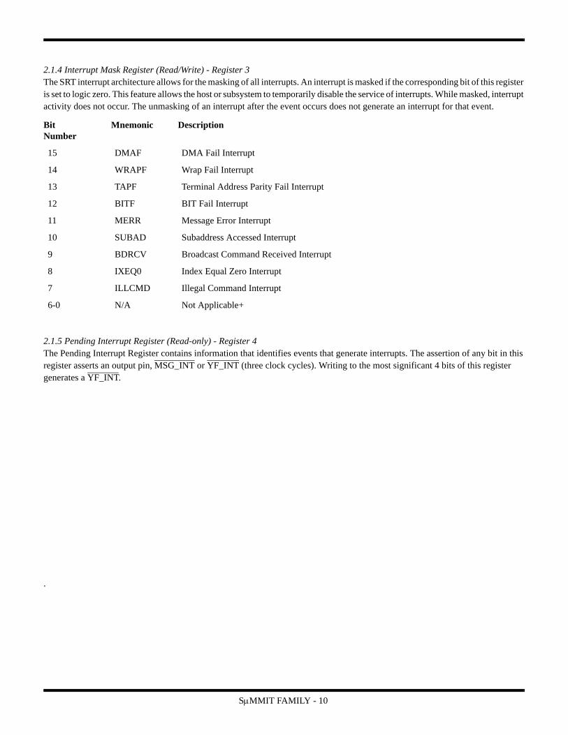
2.1.4 Interrupt Mask Register (Read/Write) - Register 3The SRT interrupt architecture allows for the masking of all interrupts. An interrupt is masked if the corresponding bit of this register is set to logic zero. This feature allows the host or subsystem to temporarily disable the service of interrupts. While masked, interrupt activity does not occur. The unmasking of an interrupt after the event occurs does not generate an interrupt for that event.
2.1.5 Pending Interrupt Register (Read-only) - Register 4The Pending Interrupt Register contains information that identifies events that generate interrupts. The assertion of any bit in this register asserts an output pin, MSG_INT or YF_INT (three clock cycles). Writing to the most significant 4 bits of this register generates a YF_INT.
.
Bit Mnemonic DescriptionNumber
15 DMAF DMA Fail Interrupt
14 WRAPF Wrap Fail Interrupt
13 TAPF Terminal Address Parity Fail Interrupt
12 BITF BIT Fail Interrupt
11 MERR Message Error Interrupt
10 SUBAD Subaddress Accessed Interrupt
9 BDRCV Broadcast Command Received Interrupt
8 IXEQ0 Index Equal Zero Interrupt
7 ILLCMD Illegal Command Interrupt
6-0 N/A Not Applicable+

SμMMIT FAMILY - 11
Bit Mnemonic DescriptionNumber
15 DMAF DMA Fail Interrupt. Once the SμΜΜIT issues the DMAR signal, an internal timer starts. If all DMA activity (which includes DMAR to DMAG, and all wait states) is not completed by the time the counter decrements to zero, the interrupt is generated. In the SRT mode, the YF_INT interrupt is generated (if not masked), current command processing ends, and the SRT will remain on-line. Current cycle terminated, bus released.
14 WRAPF Wrap Fail Interrupt. The SRT automatically compares the transmitted word (encoder word) to the reflected decoder word via the continuous loop-back feature. If the encoder word and reflected word do not match, the WRAPF bit is asserted in the BIT Word Register and a YF_INT interrupt is generated (if not masked). The loop-back path is via the MIL-STD-1553 bus transceiver.
13 TAPF Terminal Address Parity Fail Interrupt. This bit reflects the outcome of the remote terminal address parity check. A logic one indicates a parity failure. When a parity error occurs, the SRT does not begin operation (STEX bit forced to logic zero), channel A and B do not enable, the TAPF bit is asserted here and in the BIT Word Register, and a YF_INT interrupt is generated (if not masked).
12 BITF BIT Fail Interrupt. Assertion of this bit indicates a BIT failure. Status word bit 19 is automatically set to a logic one when a BIT failure occurs. If a BIT fails, the BITF bit is asserted here and in the BIT Word Register, and a YF_INT interrupt is generated (if not masked). Operation continues.
11 MERR Message Error Interrupt. Assertion of this bit indicates that a message error condition exists. The SRT can detect Manchester errors, sync-field, word count errors (too many or too few), MIL-STD-1553 word parity errors, bit count errors (too many or too few), and protocol errors. If not masked, this bit is always set when the SRT asserts bit 9 of the status word (e.g., illegal commands, invalid data word, etc.). MSG_INT interrupt generated (if not masked).
10 SUBAD Subaddress Accessed Interrupt. Assertion of this bit indicates a pre-selected subaddress has transacted a message. To determine the exact subaddress, the host interrogates the interrupt log IAW. MSG_INT interrupt generated (if not masked).
9 BDRCV Broadcast Command Received Interrupt. This bit is set to a logic one to indicate the SRT’s receipt of a valid broadcast command. The SRT suppresses status word transmission. MSG_INT interrupt generated (if not masked).
8 IXEQ0 Index Equal Zero Interrupt. The SRT asserts this bit to indicate the completion of a pre-defined number of commands by the SRT. Upon assertion of this interrupt, the host or subsystem updates the subaddress descriptor to prevent the potential loss of data. MSG_INT interrupt generated (if not masked).
7 ILLCMD Illegal Command Interrupt. This bit is set to a logic one to indicate the reception of an illegal command by the SRT. Upon receipt of this command, the SRT responds with a status word only; Bit 9 of the status word is set to a logic one. MSG_INT interrupt generated (if not masked).
6-0 N/A Not Applicable.
Note: The user must read or write a SμMMIT register after reading the Pending Register to invoke the automatic clear of the Pending Interrupt Register. For example, a Subaddress Access interrupt results in a Pending Interrupt Register of 040016. A read of the Pending Interrupt Register returns a value of 040016. A subsequent read of the Interrupt Mask Register (i.e., Register 3), followed by a Pending Interrupt Register read returns a value of 000016. The intervening read of the Interrupt Mask Register clears the Pending Interrupt Register at the end of the Interrupt Mask Register read.

SμMMIT FAMILY - 12
2.1.6 Interrupt Log List Pointer Register (Read/Write) - Register 5The Interrupt Log List Pointer indicates the starting address of the Interrupt Log List. The Interrupt Log List is a 32 word ring-buffer that contains information pertinent to the service of interrupts. The SμΜΜIT architecture requires the location of the Interrupt Log List on a 32-word boundary. The most significant 11 bits of this register designate the location of the Interrupt Log List within a 64K memory space. The lower 5 bits of this register should be initialized to a logic zero. The SμΜΜIT controls the lower 5 bits to implement the ring-buffer architecture. The host or subsystem reads this register to determine the location and number of interrupts within the Interrupt Log List (least significant 5 bits).
Note: Bits 15-5 indicate the starting Base address while bits 4-0 indicate the ring location of the Interrupt Log List. See section 6.0 for a description of the Interrupt Architecture.
2.1.7 BIT Word Register (Read/Write) - Register 6This register contains information on the SRT’s current health. The SRT transmits the contents of this register upon reception of a Transmit Bit Word Mode Code. The lower 8 bits of this register are user-defined.
Bit Mnemonic DescriptionNumber
15-0 INTA(15:0) Interrupt Log List Pointer Bits. (Bit 15 MSB - Bit 0 LSB).
Bit Mnemonic DescriptionNumber
15 DMAF DMA Fail. This bit is set if all DMA activity is not completed between the time DMAR asserts and when the timer decrements to zero. The DMA activity includes DMAR to DMAG and all wait states. In the event of a DMA failure, current message processing terminates; remote terminal waits for next 1553 message. DMAF asserts, and YF_INT is generated (if not masked).
14 WRAPF Wrap Fail. The SRT automatically compares the transmitted word (encoder word) to the reflected decoder word via the continuous loop-back feature. If the encoder word and reflected word do not match, the WRAPF bit asserts and a YF_INT interrupt is generated (if not masked). The loop-back path is via the MIL-STD-1553 bus transceiver. A wrap failure does not result in the terminal flag bit being set to a logical one. Message processing continues.
13 TAPF Terminal Address Parity Fail. This bit reflects the outcome of the remote terminal address parity check. A logic one indicates a parity failure. When a parity error occurs the SRT does not begin operation (STEX bit forced to a logic zero), channel A and B do not enable, and a YF_INT interrupt is generated (if not masked).
12 BITF BIT Fail. Assertion of this bit indicates a BIT failure. Bits 11 through 8 should be interrogated to determine the specific failure. Status word bit 19 is automatically set to a logic one when a BIT failure occurs. If a BIT fails, the BITF bit is asserted, and a YF_INT interrupt is generated (if not masked). Operation continues.
11 CHAF Channel A Fail. Assertion of this bit indicates a BIT test failure in Channel A.
10 CHBF Channel B Fail. Assertion of this bit indicates a BIT test failure in Channel B.
9 MSBF/UDB Memory Test Fail. Most significant memory byte failure (SμMMIT XTE). User-Defined Bits (SμMMIT E & SμMMIT LXE/DXE).
8 LSBF/UDB Memory Test Fail. Least significant memory byte failure (SμMMIT XTE). User-Defined Bits (SμMMIT E & SμMMIT LXE/DXE).
7-0 UDB(7:0) User-Defined Bits.

SμMMIT FAMILY - 13
2.1.8 Time-Tag Register (Read/Write) - Register 7The Time-Tag Register reflects the state of a 16-bit free running counter. The resolution of this counter is user-defined via input TCLK or fixed at 64μs/bit. The Time-Tag counter is automatically reset when the SRT receives a valid synchronize without data mode code. The SRT automatically loads the Time-Tag counter with the data associated with reception of a valid synchronize with data mode code. The Time-Tag counter begins operation on the rising edge of MRST or within 64μs after the receipt of a valid Reset Remote Terminal Mode Code, Synchronize with Data Mode Code, or Synchronize without Data Mode Code. When the SRT is halted (STEX = 0), the Time-Tag continues to run.Time-Tag value is captured upon command word-validation.
2.1.9 Remote Terminal Descriptor Pointer Register (Read/Write) - Register 8The SRT accesses a block of external memory to gain information on how to process a valid command. Each subaddress and mode code has a block of memory reserved for this task. Located contiguously in memory, these reserved memory locations are called a descriptor space. The Remote Terminal Descriptor Pointer Register contains an address that points to the top of this memory space. The SRT uses the T/R bit, subaddress/mode code field, and mode code to select one block within the descriptor table for message processing. The Remote Terminal Descriptor Pointer Register is static during message processing.
Bit Mnemonic DescriptionNumber
15-0 TT(15:0) Time-Tag Counter Bits. (Bit 15 MSB - Bit 0 LSB)
Bit Mnemonic DescriptionNumber
15-0 RTDA(15:0) Remote Terminal Descriptor Address Bits. (Bit 15 MSB - Bit 0 LSB)
SμMMIT FAMILY - 14
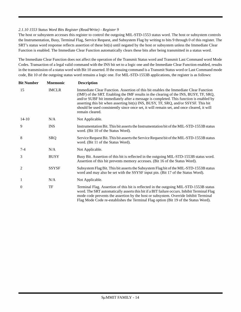
2.1.10 1553 Status Word Bits Register (Read/Write) - Register 9The host or subsystem accesses this register to control the outgoing MIL-STD-1553 status word. The host or subsystem controls the Instrumentation, Busy, Terminal Flag, Service Request, and Subsystem Flag by writing to bits 9 through 0 of this register. The SRT’s status word response reflects assertion of these bit(s) until negated by the host or subsystem unless the Immediate Clear Function is enabled. The Immediate Clear Function automatically clears these bits after being transmitted in a status word.
The Immediate Clear Function does not affect the operation of the Transmit Status word and Transmit Last Command word Mode Codes. Transaction of a legal valid command with the INS bit set to a logic one and the Immediate Clear Function enabled, results in the transmission of a status word with Bit 10 asserted. If the ensuing command is a Transmit Status word or Last Command mode code, Bit 10 of the outgoing status word remains a logic one. For MIL-STD-1553B applications, the register is as follows:
Bit Number Mnemonic Description
15 IMCLR Immediate Clear Function. Assertion of this bit enables the Immediate Clear Function (IMF) of the SRT. Enabling the IMF results in the clearing of the INS, BUSY, TF, SRQ, and/or SUBF bit immediately after a message is completed. This function is enabled by asserting this bit when asserting bit(s) INS, BUSY, TF, SRQ, and/or SSYSF. This bit should be used consistently since once set, it will remain set, and once cleared, it will remain cleared.
14-10 N/A Not Applicable.
9 INS Instrumentation Bit. This bit asserts the Instrumentation bit of the MIL-STD-1553B status word. (Bit 10 of the Status Word).
8 SRQ Service Request Bit. This bit asserts the Service Request bit of the MIL-STD-1553B status word. (Bit 11 of the Status Word).
7-4 N/A Not Applicable.
3 BUSY Busy Bit. Assertion of this bit is reflected in the outgoing MIL-STD-1553B status word. Assertion of this bit prevents memory accesses. (Bit 16 of the Status Word).
2 SSYSF Subsystem Flag Bit. This bit asserts the Subsystem Flag bit of the MIL-STD-1553B status word and may also be set with the SSYSF input pin. (Bit 17 of the Status Word).
1 N/A Not Applicable.
0 TF Terminal Flag. Assertion of this bit is reflected in the outgoing MIL-STD-1553B status word. The SRT automatically asserts this bit if a BIT failure occurs. Inhibit Terminal Flag mode code prevents the assertion by the host or subsystem. Override Inhibit Terminal Flag Mode Code re-establishes the Terminal Flag option (Bit 19 of the Status Word).

SμMMIT FAMILY - 15
For MIL-STD-1553A applications, the register is as follows:
Bit Number Mnemonic Description
15 IMCLR Immediate Clear Function. Assertion of this bit enables the Immediate Clear Function (IMF) of the SRT. Enabling the IMF results in the clearing of the bit times 10-19 immediately after a status word is transmitted. This function is enabled by asserting this bit when asserting bit times 10-19. This bit should be used consistently since once set, it will remain set, and once cleared, it will remain cleared.
14-10 N/A Not Applicable.
9 SB10 Status bit time 10.
8 SB11 Status bit time 11.
7 SB12 Status bit time 12.
6 SB13 Status bit time 13.
5 SB14 Status bit time 14.
4 SB15 Status bit time 15.
3 SB16 Status bit time 16.
2 SB17 Status bit time 17.
1 SB18 Status bit time 18.
0 SB19 Status bit time 19.

SμMMIT FAMILY - 16
2.1.11 Illegalization RegistersThe 16 registers are divided into 8 blocks, 2 registers per block (see table 1).
Table 1. Illegalization Register Blocks
The blocks correspond to the following types of commands. Register address 0010 (hex) and 0011 (hex) illegalize receive commands to 32 subaddresses. The most significant bit of register 0010 (hex) controls the illegalization of subaddress 01111. The least significant bit controls subaddress 00000. Register 0011 (hex) controls illegalization of subaddresses 10000 through 11111. The least significant bit relates to subaddress 10000; the most significant bit relates to subaddress 11111. Transmit commands and broadcast commands (both receive and transmit) use the same encoding scheme as receive subaddress illegalization.
Registers 18 (hex) through 1F (hex) control the illegalization of mode codes. Register 18 governs the illegalization of receive mode codes (T/R bit = 0) 00000 through 01111 and register 19 mode codes 10000 through 11111. Register blocks Transmit Mode Code (T/R bit = 1), Broadcast Receive Mode Codes, and Broadcast Transmit Mode Codes use the same decode scheme as receive mode codes.
Table 2 shows the illegalization register map. For each block, the numbers shown in the column under each bit number identifies the specific subaddress or mode code (in hex) that the register bit illegalizes (Logical 0 = legal, Logical 1 = illegal).
Block Name Address (hex)
Receive 0010 and 0011
Transmit 0012 and 0013
Broadcast Receive 0014 and 0015
Broadcast Transmit (Automatically Illegalized)
0016 and 0017
Mode Code Receive 0018 and 0019
Mode Code Transmit 001A and 001B
Broadcast Mode Code Receive 001C and 001D
Broadcast Mode Code Transmit 001E and 001F

SμMMIT FAMILY - 17
Table 2. Illegalization Register Map
Notes:1. Brd = Broadcast. 2. Mode = Mode code. 3. XX= Automatically illegalized by SRT. 4. YY= Automatically illegalized by SRT in 1553B only. 5. ZZ= Automatically illegalized by SRT in 1553B and 1553A if XMTSW is enabled. 6. WW = Automatically illegalized in 1553A.7. UU = Automatically illegalized in 1553A if XMTSW enabled.
Name Register Number
Bit Number 15 14 13 12 11 10 9 8 7 6 5 4 3 2 1 0
Receive 16 0F 0E 0D 0C 0B 0A 09 08 07 06 05 04 03 02 01 00
17 1F 1E 1D 1C 1B 1A 19 18 17 16 15 14 13 12 11 10
Transmit 18 0F 0E 0D 0C 0B 0A 09 08 07 06 05 04 03 02 01 00
19 1F 1E 1D 1C 1B 1A 19 18 17 16 15 14 13 12 11 10
Brd Receive 20 0F 0E 0D 0C 0B 0A 09 08 07 06 05 04 03 02 01 00
21 1F 1E 1D 1C 1B 1A 19 18 17 16 15 14 13 12 11 10
Brd Transmit 22 XX XX XX XX XX XX XX XX XX XX XX XX XX XX XX XX
23 XX XX XX XX XX XX XX XX XX XX XX XX XX XX XX XX
Mode Receive 24 0F 0E 0D 0C 0B 0A 09 08 07 06 05 04 03 02 01 00
25 1F 1E 1D 1C 1B 1A 19 18 17 16 15 14 13 12 11 10
Mode Transmit 26 0F 0E 0D 0C 0B 0A 09 08 07 06 05 04 03 02 01 00
27 1F 1E 1D 1C 1B 1A 19 18 17 16 15 14 13 12 11 10
Mode Brd Receive 28 0F 0E 0D 0C 0B 0A 09 08 07 06 05 04 03 UU 01 WW
29 1F 1E 1D 1C 1B 1A 19 18 17 16 15 14 13 12 11 10
Mode Brd Transmit 30 0F 0E 0D 0C 0B 0A 09 08 07 06 05 04 03 ZZ 01 XX
31 YY YY YY YY YY YY YY YY YY YY YY YY YY YY YY YY

SμMMIT FAMILY - 18
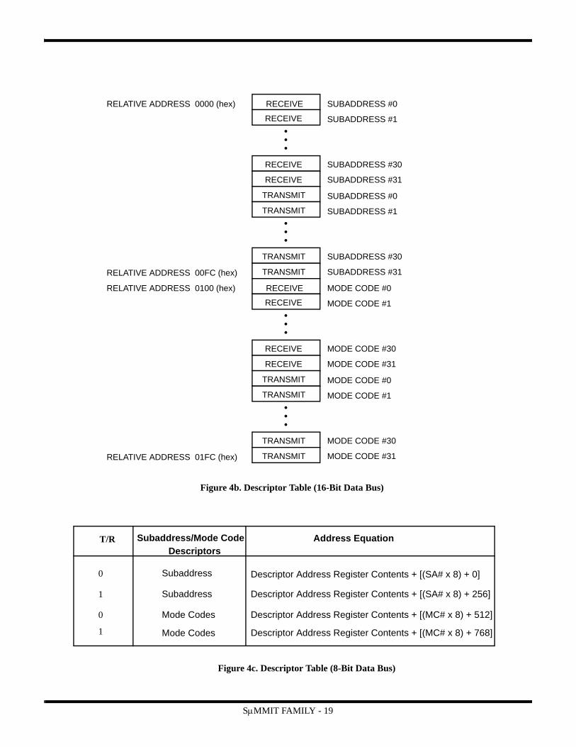
2.2 Descriptor BlockTo process messages, the SRT uses data supplied in the internal registers with data stored in external memory. The SRT accesses a four word descriptor block stored in external memory. The descriptor block is accessed at the beginning and end of command processing. Multiple descriptor blocks are sequentially entered into memory to form a descriptor table. The following paragraphs discuss the descriptor block in detail.
The host or subsystem controlling the SRT allocates 512 consecutive memory spaces for the subaddress and mode code descriptor table. The top of the descriptor table can reside at any address location. Defined and entered into memory by the host, the SRT is linked to the descriptor table via the Descriptor Address Register contents (see figures 4a and 4b). Each descriptor block contains a Control Word, Data Pointer A, Data Pointer B, and Broadcast Data Pointer. Each subaddress and mode code is assigned a descriptor for receive and transmit commands (T/R bit equal zero or one).
Control word information allows the SRT to generate interrupts, buffer messages, and control message processing. For a receive command, the Data Pointer is read to determine the top of the data buffer. The SRT stores data sequentially from the top of data buffer plus two locations (e.g., 0100, 0101, 0102, 0103, etc.). When processing a transmit command, the Data Pointer is read to determine where data words are retrieved. The SRT retrieves data words sequentially from the address the Data Pointer designates plus two address locations.
The Broadcast Data Pointer allows for separate storage of non-broadcast data from broadcast data per MIL-STD-1553B Notice II. The host or subsystem enables or disables this feature via the Control Word’s least significant bit. When disabled, the non-
broadcast and broadcast data is stored via Data List Pointer A or B. For transmit commands, the Broadcast Data Pointer is not used. The SRT does not transmit any information on the receipt of a broadcast transmit command.
The SRT reads the descriptor block during command processing (i.e., after assertion of TERACT). The SRT arbitrates for the memory bus. After receiving control of the bus, the SRT reads the control word and three Data Pointers. The SRT then surrenders control of the bus back to the bus master (i.e., negates DMACK). The SRT then begins the acquisition of data words for either transmission or storage.
After transmission or reception, the SRT begins post-processing. Command post-processing begins with arbitration for the memory bus. The SRT performs a DMA burst during post-processing. An optional interrupt log entry is performed after a descriptor update. During the descriptor update, the SRT modifies the Control Word index field and bits 4, 2, and 1, if required. The SRT updates Data Pointer A if no message errors occurred during the message transaction. Reception of a broadcast command, with no message errors, results in the update of the Broadcast Data Pointer. Neither Data Pointer A, B or Broadcast is updated if the SRT has the ping-pong mode of operation enabled.
See section 5, Enhanced SμMMIT Family Operation for additional information.
Subaddress/Mode Code Address Equation
Subaddress Descriptor Address Register Contents + [(SA# x 4) + 0]
Subaddress Descriptor Address Register Contents + [(SA# x 4) + 128]
Descriptor Address Register Contents + [(MC# x 4) + 256]
Descriptor Address Register Contents + [(MC# x 4) + 384]
Figure 4a. Descriptor Table (16-Bit Data Bus)
Descriptors
Mode Codes
Mode Codes
0
0
1
1
T/R
SμMMIT FAMILY - 19
RECEIVE
RECEIVE•••
RECEIVE
RECEIVE
TRANSMIT
TRANSMIT
SUBADDRESS #0
SUBADDRESS #1
SUBADDRESS #30
SUBADDRESS #31
SUBADDRESS #0
SUBADDRESS #1
TRANSMIT
TRANSMIT
•••
SUBADDRESS #30
SUBADDRESS #31
RELATIVE ADDRESS 0000 (hex)
RELATIVE ADDRESS 00FC (hex)
RECEIVE
RECEIVE•••
RECEIVE
RECEIVE
TRANSMIT
TRANSMIT
MODE CODE #0
MODE CODE #1
MODE CODE #30
MODE CODE #31
MODE CODE #0
MODE CODE #1
TRANSMIT
TRANSMIT
•••
MODE CODE #30
MODE CODE #31
RELATIVE ADDRESS 0100 (hex)
RELATIVE ADDRESS 01FC (hex)
Figure 4b. Descriptor Table (16-Bit Data Bus)
Subaddress/Mode Code Address Equation
Subaddress Descriptor Address Register Contents + [(SA# x 8) + 0]
Subaddress Descriptor Address Register Contents + [(SA# x 8) + 256]
Descriptor Address Register Contents + [(MC# x 8) + 512]
Descriptor Address Register Contents + [(MC# x 8) + 768]
Figure 4c. Descriptor Table (8-Bit Data Bus)
Descriptors
Mode Codes
Mode Codes
0
0
1
1
T/R

SμMMIT FAMILY - 20
RECEIVE
RECEIVE•••
RECEIVE
RECEIVE
TRANSMIT
TRANSMIT
SUBADDRESS #0
SUBADDRESS #1
SUBADDRESS #30
SUBADDRESS #31
SUBADDRESS #0
SUBADDRESS #1
TRANSMIT
TRANSMIT
•••
SUBADDRESS #30
SUBADDRESS #31
RELATIVE ADDRESS 0000 (hex)
RELATIVE ADDRESS 01F8 (hex)
RECEIVE
RECEIVE•••
RECEIVE
RECEIVE
TRANSMIT
TRANSMIT
MODE CODE #0
MODE CODE #1
MODE CODE #30
MODE CODE #31
MODE CODE #0
MODE CODE #1
TRANSMIT
TRANSMIT
•••
MODE CODE #30
MODE CODE #31
RELATIVE ADDRESS 0200 (hex)
RELATIVE ADDRESS 03F8 (hex)
Figure 4d. Descriptor Table (8-Bit Data Bus)

SμMMIT FAMILY - 21
2.2.1 Receive Control WordThe following bits describe the receive subaddress Descriptor Control Word. Information contained in this word assists the SRT in message processing. The Descriptor Control Word is initialized by the host or subsystem and updated by the SRT during command post-processing.
Bit Mnemonic DescriptionNumber
15-8 INDX Index Field. These bits define multiple message buffer length. The host or subsystem uses this field to instruct the SRT to buffer “N” messages. “N” can range from 0 (00 hex) to 255 (FF hex). If buffer ping-ponging is enabled, the INDX field is “don’t care” (i.e., does not contain applicable information). During ping-pong mode operation, initialize the index field to 00 (hex). The SRT does not perform multiple message buffering in the ping-pong mode of operation. The index decrements each time a complete message is transacted (no message errors). The index does not decrement if the subaddress is illegalized. The SRT can generate an interrupt when the index field transitions from one to zero (see bit 7).
7 INTX Interrupt Index Equals Zero. Assertion of this bit enables the generation of an interrupt when the index field transitions from one to zero. The interrupt is entered into the Pending Interrupt Register if not masked in the Mask Register. Output pin MSG_INT asserts after message processing.
6 IWA Interrupt When Accessed. Assertion of this bit enables the generation of an interrupt when the subaddress receives a valid command; this includes illegal and broadcast commands. The interrupt is entered into the Pending Interrupt Register if not masked in the Mask Register. Output pin MSG_INT asserts after message processing.
5 IBRD Interrupt Broadcast Received. Assertion of this bit enables the generation of an interrupt when the subaddress receives a valid broadcast command. The interrupt is entered into the Pending Interrupt Register if not masked in the Mask Register. Output pin MSG_INT asserts after message processing.
4 BAC Block Accessed. The subsystem or host initializes this bit to zero; the SRT overwrites the zero with a logic one upon completion of message processing. After interrogating this bit, the host resets this bit to zero to observe further accesses.
3 N/A Not Applicable.
2 A/B Buffer A/B. Indicates the last buffer accessed when buffer ping-pong is enabled. During initialization, the host designates the first buffer used by asserting or negating this bit. A logic one indicates buffer A; a logic zero indicates buffer B. This bit is a “don’t care” if buffer ping-ponging is not enabled.
1 BRD Broadcast Received. Assertion of this bit indicates the reception of a valid broadcast command.
0 NII Notice II. Assertion of this bit enables the use of the Broadcast Data Pointer as a buffer for broadcast command information. When negated, broadcast information is stored in the same buffer as non-broadcast information.

SμMMIT FAMILY - 22
2.2.2 Transmit Control WordThe following bits describe the transmit subaddress Descriptor Control Word. Information contained in this word assists the SRT in message processing. The Descriptor Control Word is initialized by the host or subsystem and updated by the SRT during command post-processing.
Bit Mnemonic DescriptionNumber
15-7 N/A Not Applicable.
6 IWA Interrupt When Accessed. Assertion of this bit enables the generation of an interrupt when the subaddress receives a valid command; his includes illegal and broadcast commands. The interrupt is entered into the Pending Interrupt Register if not masked in the Mask Register. Output pin MSG_INT asserts after message processing.
5 N/A Not Applicable.
4 BAC Block Accessed. The subsystem or host initializes this bit to zero, the SRT overwrites the zero with a logic one upon completion of message processing. After interrogation, the host should reset this bit to zero to observe further accesses.
3 N/A Not Applicable.
2 A/B Buffer A/B. Indicates the data pointer to access when buffer ping-pong is enabled. During initialization, the host designates the first buffer used by asserting or negating this bit. A logic one indicates buffer A; a logic zero indicates buffer B. This bit is a “don’t care” if buffer ping-ponging is not enabled.
1 BRD Broadcast Received. Assertion of this bit indicates the reception of a broadcast command.
0 N/A Not Applicable.

SμMMIT FAMILY - 23
2.2.3 Mode Code Receive Control WordThe following bits describe the receive mode code Descriptor Control Word. Information contained in this word assists the SRT in message processing. The Descriptor Control Word is initialized by the host or subsystem and updated by the SRT during command post-processing.
Note: In MIL-STD-1553A, all mode codes are without data, and the T/R bit is ignored. See section 2.9 for the MIL-STD-1553A operation.
Bit Mnemonic DescriptionNumber
15-8 INDX Index Field. These bits define message buffer length. The host or subsystem uses this field to instruct the SRT to buffer “N” messages. “N” can range from 0 (00 hex) to 256 (FF hex). If buffer ping-ponging is enabled, the INDX field is “don’t care” (i.e., does not contain applicable information). The SRT does not perform message buffering in the ping-pong mode of operation. The index decrements each time a complete message is transacted (no message errors). The index does not decrement if the mode code is illegalized. The SRT can generate an interrupt when the index field transitions from one to zero (see bit 7).
7 INTX Interrupt Index Equals Zero. Assertion of this bit enables the generation of an interrupt when the index field transitions from one to zero. The interrupt is entered into the Pending Interrupt Register if not masked in the Mask Register. Output pin MSG_INT asserts after message processing.
6 IWA Interrupt When Accessed. Assertion of this bit enables the generation of an interrupt when mode code command is received; his includes illegal and broadcast commands. The interrupt is entered into the Pending Interrupt Register if not masked in the Mask Register. Output pin MSG_INT asserts after message processing.
5 IBRD Interrupt Broadcast Received. Assertion of this bit enables the generation of an interrupt when a valid broadcast mode code command is received. The interrupt is entered into the Pending Interrupt Register if not masked in the Mask Register. Output pin MSG_INT asserts after message processing.
4 BAC Block Accessed. The subsystem or host initializes this bit to zero; the SRT overwrites the zero with a logic one upon completion of message processing. After interrogating this bit, the host resets this bit to zero to observe further accesses.
3 N/A Not Applicable.
2 A/B Buffer A/B. Indicates the last buffer accessed when buffer ping-pong is enabled. During initialization, the host designates the first buffer used by asserting or negating this bit. A logic one indicates buffer A; logic zero indicates buffer B. This bit is a “don’t care” if buffer ping-ponging is not enabled.
1 BRD Broadcast Received. Assertion of this bit indicates the reception of a valid broadcast command.
0 NII Notice II. Asserting this bit enables the use of the Broadcast Data Pointer as a buffer for broadcast command information. When negated, broadcast information is stored in the same buffer as non-broadcast information.

SμMMIT FAMILY - 24
2.2.4 Mode Code Transmit Control WordThe following bits describe the transmit mode code Descriptor Control Word. Information contained in this word assists the SRT in message processing. The Descriptor Control Word is initialized by the host or subsystem and updated by the SRT during command post-processing.
Note: In MIL-STD-1553A, all mode codes are without data, and the T/R bit is ignored. See section 2.9 for the MIL-STD-1553A operation.
Bit Mnemonic DescriptionNumber
15-7 N/A Not Applicable.
6 IWA Interrupt When Accessed. Assertion of this bit enables the generation of an interrupt when mode code command is received; his includes illegal and broadcast commands. The interrupt is entered into the Pending Interrupt Register if not masked in the Mask Register. Output pin MSG_INT asserts after message processing.
5 IBRD Interrupt Broadcast Received. Assertion of this bit enables the generation of an interrupt when a valid broadcast mode code is received. The interrupt is entered into the Pending Interrupt Register if not masked in the Mask Register. Output pin MSG_INT asserts after message processing.
4 BAC Block Accessed. The subsystem or host initializes this bit to zero; the SRT overwrites the zero with a logic one upon completion of message processing. After interrogating this bit, the host resets this bit to zero to observe further accesses.
3 N/A Not Applicable.
2 A/B Buffer A/B. This bit indicates the last buffer accessed when buffer ping-pong is enabled. During initialization, the host designates the first buffer used by asserting or negating this bit. A logic one indicates buffer A; a logic zero indicates buffer B. This bit is a “don’t care” if buffer ping-ponging is not enabled.
1 BRD Broadcast Received. Assertion of this bit indicates the reception of a broadcast command.
0 N/A Not Applicable.

SμMMIT FAMILY - 25
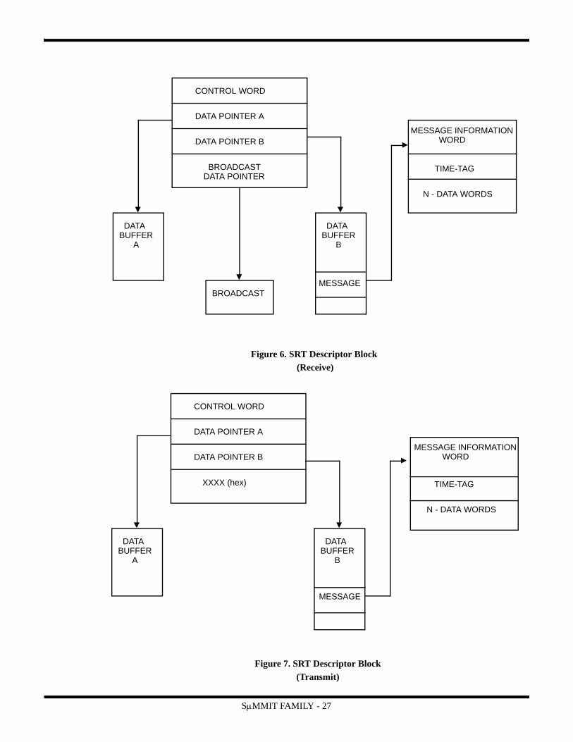
2.2.5 Data Pointer A and BData Pointer A and B contain address information for the retrieval and storage of message data words. In the index mode of operation, the SRT reads Data Pointer A to determine the location of data for retrieval or storage. The SRT uses the Data Pointer to initialize an internal counter; the counter increments after each data word. For a receive command, the SRT stores the incoming data word sequentially into memory. As part of command post-processing, the SRT writes a new data pointer into the descriptor block. The SRT continues to update the data pointer until the Control Word index field decrements to zero. An example is shown in figure 5.
Note: The index feature is not applicable for transmit commands (i.e., T/R bit = 1).
For ping-pong buffer operation, the host uses either Data Pointer A or Data Pointer B. The SRT determines which pointer to access via the state of Control Word bit 2. The SRT retrieves or stores data words from the address contained in the data pointer, automatically incrementing the data pointer as data words are received. The data pointer is never updated as part of command post-processing in the ping-pong mode of operation. See figures 6 and 7.
2.2.6 Broadcast Data PointerThe following bits describe the receive subaddress/mode code descriptor Broadcast Data Pointer. This word contains the address for the Message Information word, Time-Tag word, and data words associated with a broadcast command. The SRT automatically increments this data pointer during command post-processing, if ping-pong operation disabled.
2.3 Data StructuresThe following sections discuss the data structures that result from command processing. For each complete message processed, the SRT generates a Message Information word and Time-Tag word. These words aid the host or subsystem
in further message processing. The Message Information word contains word count, message type, and message error information. The Time-Tag word is a 16-bit word containing the command validity time. The Time-Tag word data comes from the SRT’s internal Time-Tag counter.
See section 5, Enhanced Family SμMMIT Operation for additional data structure information
Bit Mnemonic DescriptionNumber
15-0 DP(15:0) Data Pointer Bits. The second and third words of the descriptor block contain the data buffer location. The SRT accesses either Data Pointer A or Data Pointer B depending on the state of Control Word Bit 2 during ping-pong operation. For index operation, the SRT accesses only Data Pointer A. The SRT updates Data Pointer A after message processing is complete and the index field is not equal to zero and ping-pong operation disabled. Bit 15 is the most significant bit; bit 0 is the least significant bit.
Bit Mnemonic DescriptionNumber
15-0 BP(15:0) Broadcast Data Pointer. The fourth word of the descriptor block contains the broadcast data buffer location. This pointer can reside anywhere inside of a 64K data space. The SRT accesses this pointer when Control Word bit 0 is a logic one and broadcast is enabled. Bit 15 is the most significant bit; bit 0 is the least significant bit.Note: If ping-pong is enabled, this pointer does not update.Note: When the broadcast command is followed by a Transmit Last Command or Transmit Status Word mode code, the SRT transmits a status word with bit 15 of the status word set to a logic one. The broadcast bit is cleared by reception of the next valid non-broadcast command.

SμMMIT FAMILY - 26
Figure 5. Non-Broadcast Receive Message Indexing
0100 (hex)
0101 (hex)
0102 (hex)
0103 (hex)
0104 (hex)
0105 (hex)
0106 (hex)
0107 (hex)
0108 (hex)
0109 (hex)
010A (hex)
010B (hex)
010C (hex)
010D (hex)
Index equals two
Index decrements to one
Index equals one
Index decrements to zero(interrupt generated if enabled)
Index equals zero
Index remains zero(Data Pointer A = 109)
Message Info Word
Time-Tag
Data Word #1
Data Word #2
Data Word #3
Message Info Word
Time-Tag
Data Word #1
Data Word #2
Message Info Word
Time-Tag
Data Word #1
Data Word #2
Data Word #3
Command #1Receive three words
Command #2Receive two words
Command #3Receive three words
CONTROL WORD
DATA POINTER A
DATA POINTER B
BROADCAST
Receive Subaddress #1Descriptor Block
Index field contents: 02XX (hex)
Data Pointer A: 0100 (hex)
Data Pointer B: XXXX (hex)
Broadcast Data Pointer: XXXX (hex)
Note:x = “don’t care”
SμMMIT FAMILY - 27
Figure 6. SRT Descriptor Block (Receive)
CONTROL WORD
DATA POINTER A
DATA POINTER B
BROADCASTDATA POINTER
DATABUFFER A
DATABUFFER B
BROADCASTMESSAGE
MESSAGE INFORMATION WORD
TIME-TAG
N - DATA WORDS
CONTROL WORD
DATA POINTER A
DATA POINTER B
XXXX (hex)
DATABUFFER A
DATABUFFER B
MESSAGE
MESSAGE INFORMATION WORD
TIME-TAG
N - DATA WORDS
Figure 7. SRT Descriptor Block (Transmit)

SμMMIT FAMILY - 28
2.3.1 Subaddress Receive DataFor receive commands, the SRT stores data words plus two additional words. The SRT adds a Receive Information word and Time-Tag word to each receive command data packet. The SRT places the Receive Information word and Time-Tag word ahead of the data words associated with a receive command (see figures 5, 6 and 7). When message errors occur, the SRT enters the Receive Information word, and Time-Tag word. Once a message error condition is observed, all data words are considered invalid.
Data storage occurs at the memory location pointed to by the data pointer plus two locations.
2.3.1.1 Receive Information (Info) WordThe following bits describe the Receive Information Word contents.
2.3.2 Subaddress Transmit DataThe host or subsystem is responsible for organization of the data packet (i.e., N data words) into memory and establishing the applicable data pointer. The host or subsystem allocates two memory locations at the top of the data packet for the storage of the Transmit Information word and Time-Tag word. An example transmit data structure for three words is shown below.
Data Pointer A -----> 0100 (hex) XXXX ;reserved for Transmit Info word equals 0100 (hex) 0101 (hex) XXXX ;reserved for Time-Tag word
0102 (hex) FFFF ;data word 0103 (hex) FFFF ;data word 0104 (hex) FFFF ;data word
Note: Data Pointer A points to the top of the data structure not to the top of the data words.
Bit Mnemonic DescriptionNumber
15-11 WC(4:0) Word Count Bits. These five bits contain word count information extracted from the transmit command word bits 15 to 19.
10 N/A Not Applicable.
9 CHA/B Channel A/B. Assertion of this bit indicates that the message was received on channel A. Conversely, if this bit is set to logic zero, the message was received on channel B.
8 RTRT Remote Terminal to Remote Terminal transfer. The command processed was a RT-to-RT transfer.
7 ME Message Error. Assertion of this bit indicates a message error condition was observed during processing. See bits 0 to 4 for details.
6-5 N/A Not Applicable.
4 ILL Illegal Command Received. Assertion of this bit indicates the command received was an illegal command.
3 TO Time-Out Error. Assertion of this bit indicates the SRT did not receive the proper number of data words, i.e., the number of data words received was less than the word count specified in the command word.
2 OVR Overrun Error. Assertion of this bit indicates the SRT received a word when none was expected or the number of data words received was greater than expected.
1 PRTY Parity Error. Assertion of this bit indicates the SRT observed a parity error in the incoming data words.
0 MAN Manchester Error. Assertion of this bit indicates the SRT observed a Manchester error in the incoming data words.

SμMMIT FAMILY - 29
2.3.2.1 Transmit Information (Info) WordThe following bits describe the Transmit Information word contents.
2.3.3 Mode Code DataThe transmit and receive data structures for mode codes are similar to those for subaddress. The receive data structure contains an Information word, Time-Tag word, and message data word. All receive mode codes with data have one associated data word. Data storage occurs at the memory location pointed to by the data pointer plus two locations. Reception of the synchronize with data mode code automatically loads the Time-Tag counter and stores the data word at the address defined by the data pointer plus two locations.
The transmit mode code data structure contains an Information word, Time-Tag word, and associated data word. The subsystem or host is responsible for linking the SRT Data Pointer to the data (e.g., Transmit Vector word). For mode codes with internally generated data words (e.g., Transmit BIT word, Transmit Last Command), the transmitted data word is added to the data structure.
For MIL-STD-1553A mode of operation, all mode codes are defined without data words. For mode codes without data, the data structure contains the Message Information word and Time-Tag word only.
Note: In MIL-STD-1553A, all mode codes are without data and the T/R bit is ignored. See section 2.9 for the MIL-STD-1553A operation.
Bit Mnemonic DescriptionNumber
15-11 WC(4:0) Word Count Bits. These five bits contain word count information extracted from the receive command word bits 15 to 19.
10 N/A Not Applicable.
9 CHA/B Channel A/B. Assertion of this bit indicates that the message was received on the A bus. Conversely, if this bit is set to logic zero, the message was received on the B bus.
8 N/A Not Applicable.
7 ME Message Error. Assertion of this bit indicates a message error condition was observed during processing. See bits 0 to 4 for more detail.
6-5 N/A Not Applicable.
4 ILL Illegal Command Received. Assertion of this bit indicates the command received was an illegal command.
3 N/A Not Applicable.
2 OVR Overrun Error. Assertion of this bit indicates the SRT received a data word with a Transmit Command.
1-0 N/A Not Applicable.

SμMMIT FAMILY - 30
2.3.3.1 Mode Code Receive Information (Info) Word. The following bits describe the Mode Code Receive Information word contents.
2.3.3.2 Mode Code Transmit Information (Info) Word. The following bits describe the Mode Code Transmit Information word contents.
Bit Mnemonic DescriptionNumber
15-11 MC (4:0) Mode Code. These five bits contain the mode code information extracted from the receive command word bits 15 to 19.
10 N/A Not Applicable.
9 CHA/B Channel A/B. Assertion of this bit indicates that the message was received on the A bus. Conversely, if this bit is set to logic zero, the message was received on the B bus.
8 RTRT Remote Terminal to Remote Terminal transfer. Assertion of this bit indicates the command processed was a RT-to-RT transfer.
7 ME Message Error. Assertion of this bit indicates a message error condition was observed during processing. See bits 0 to 4 for details.
6-5 N/A Not Applicable.
4 ILL Illegal Command Received. Assertion of this bit indicates the command received was an illegal command.
3 TO Time-out Error. Assertion of this bit indicates the SRT did not receive the proper number of data words, i.e., the number of data words received was less than the word count specified in the command word.
2 OVR Overrun Error. Assertion of this bit indicates the SRT received a word when none was expected, or the number of data words received was greater than expected.
1 PRTY Parity Error. Assertion of this bit indicates the SRT observed a parity error in the incoming data words.
0 MAN Manchester Error. Assertion of this bit indicates the SRT observed a Manchester error in the incoming data words.
Bit Mnemonic DescriptionNumber
15-11 MC (4:0) Mode Code. These five bits contain the mode code information extracted from the command word bits 15 to 19.
10 N/A Not Applicable.
9 CHA/B Channel A/B. Assertion of this bit indicates that the message was received on the A bus. Conversely, if this bit is set to logic zero, the message was received on the B bus.
8 N/A Not Applicable.
7 ME Message Error. Assertion of this bit indicates a message error condition was observed during processing. See bits 0 to 4 for details.
6-5 N/A Not Applicable.
4 ILL Illegal Command Received. Assertion of this bit indicates the command received was an illegal command.
3 N/A Not Applicable.
2 OVR Overrun Error. Assertion of this bit indicates the SRT received a data word with a Transmit Command.
1-0 N/A Not Applicable.

SμMMIT FAMILY - 31
2.4 Mode Code and SubaddressThe SμΜΜIT provides subaddress and mode code decoding that meets MIL-STD-1553B requirements. In addition, the
device has automatic internal illegal command decoding for reserved MIL-STD-1553B mode codes. Table 3 shows the SRT’s response to all possible mode code combinations.
Table 3. Mode Code DescriptionsT/R Mode Code Function Operation
0 00000-01111 Undefined (w/o data) 1. Command word stored 2. Status word transmitted
0 10000 Undefined (with data) 1. Command word stored 2. Data word stored 3. Status word transmitted
0 10001 Synchronize (with data) 1. Command word stored 2. Data word stored 3. Time-Tag counter loaded with data word value 4. Status word transmitted
0 10010 Undefined 1. Command word stored 2. Data word stored 3. Status word transmitted
0 10011 Undefined 1. Command word stored 2. Data word stored 3. Status word transmitted
0 10100 Selected Transmitter Shutdown
1. Command word stored 2. Data word stored 3. Status word transmitted
0 10101 Override Selected Transmitter Shutdown
1. Command word stored 2. Data word stored3. Status word transmitted
0 10110-11111 Reserved 1. Command word stored 2. Data word stored 3. Status word transmitted
1 00000 Dynamic Bus Control 1. Command word stored 2. Dynamic Bus Acceptance bit set in outgoing
status word if enabled in the Control Register3. Status word transmitted
1 00001 Synchronize 1. Command word stored 2. Time-Tag counter reset to 0000 (hex) 3. Status word transmitted
1 00010 Transmit Status Word 1. Command word stored2. Last status word transmitted3. Status word cleared after master reset
Note: SRT updates status word if illegalized.
1 00011 Initiate Self-Test 1. Command word stored 2. Status word transmitted 3. BIT initiated4. TF bit set if BITF bit asserted
1 00100 Transmitter Shutdown 1. Command word stored 2. Status word transmitted3. Alternate bus disabled

SμMMIT FAMILY - 32
Table 3. Mode Code Descriptions (Cont.)
T/R Mode Code Function Operation
1 00101 Override Transmitter Shutdown
1. Command word stored 2. Status word transmitted 3. Alternate bus enabledNote: Reception of the override transmitter shutdown mode code does not enable a channel not previously enabled in the Control Register. Reset remote terminal mode code clears the transmitter shutdown function.
1 00110 Inhibit Terminal Flag Bit 1. Command word stored 2. Terminal flag bit set to zero and assertion
disabled3. Status word transmitted
1 00111 Override Inhibit Terminal Flag
1. Command word stored 2. Terminal Flag bit enabled for assertion 3. Status word transmitted
1 01000 Reset Remote Terminal 1. Command word stored 2. Status word transmitted 3. SRT reset, see section 2.8 for more
information on software reset
1 01001-01111 Reserved 1. Command word stored 2. Status word transmitted
1 10000 Transmit Vector Word 1. Command word stored 2. Service request bit set to a logic zero in out going
status3. Status word transmitted 4. Data word transmitted 5. Clears the SRQ bit in the 1553 status word bits
register (Register 9)
1 10001 Reserved 1. Command word stored 2. Status word transmitted 3. Data word transmitted
1 10010 Transmit Last Command 1. Command word not stored 2. Last status word transmitted 3. Last command word transmitted 4. Data word stored (Transmit Last Command)5. Transmitted data word is all zero after resetNote: The SRT stores the Transmit Last Command mode code if illegalized and updates status word.
1 10011 Transmit BIT Word 1. Command word stored 2. Status word transmitted 3. BIT word transmitted from BIT Word Register 4. Data word stored (Transmit BIT Word)
1 10100-10101 Undefined (with data) 1. Command word stored 2. Status word transmitted 3. Data word transmitted
1 10110-11111 Reserved 1. Command word stored 2. Status word transmitted 3. Data word transmitted

SμMMIT FAMILY - 33
2.5 Encoder and DecoderThe SRT interfaces directly to a transmitter/receiver via the SRT Manchester II encoder/decoder. The SRT receives the command word from the MIL-STD-1553 bus and processes it either by the primary or secondary decoder. Each decoder checks for the proper sync pulse and Manchester waveform, edge skew, correct number of bits, and parity. If the command is a receive command, the SRT processes each incoming data word for correct format, word count, and contiguous data. If a message error is detected, the SRT stops processing the remainder of the message (i.e., DMAs), suppresses status word transmission, and asserts bit 9 (ME bit) of the status word. The SRT will track the message until proper word count is finished.
The SRT automatically compares the transmitted word (encoder word) to the reflected decoder word by way of the continuous loop-back feature. If the encoder word and reflected word do not match, the WRAPF bit is asserted in the BIT Word Register and the YF_INT will be generated, if enabled. In addition to the loop-back compare test, a timer precludes a transmission greater than 800μs by the assertion of Fail-Safe Timer (TIMERONA or TIMERONB). This timer is reset upon receipt of another command. Remote Terminal Response Time:
MIL-STD-1553A = 7μsMIL-STD-1553B = 10μsData Contiguity Time-Out = 1.0μs
2.6 RT-RT Transfer CompareThe RT-to-RT Terminal Address compare logic ensures that the incoming status word’s Terminal Address matches the Terminal Address of the transmitting RT specified in the command word. An incorrect match results in setting the message-error bit and suppressing transmission of the status word. (RT-to-RT transfer time-out = 55 to 59μs). The receiving SRT does not check ME or SSYSF of the transmitting remote terminal.
2.7 Terminal AddressThe SRT Terminal Address is programmed via six input pins: RTA(4:0) and RTPTY. Negating MRST latches the SRT’s Terminal Address from pins RTA(4:0) and parity bit RTPTY. The address and parity cannot change until the next assertion and negation of the MRST input (for LOCK = 0). The Terminal Address parity is odd; input pin RTPTY is set to a logic state to satisfy this requirement. Assertion of Operational Status Register bit 2 (TAPF) indicates incorrect Terminal Address parity. The Operational Status Register bit 2 is valid after the rising edge of MRST.
For example:
RTA(4:0) = 05 (hex) = 00101 (binary) RTPTY = 1, Sum of 1s = 3 (odd), Operational Status Register Bit 2 = 0
RTA(4:0) = 04 (hex) = 00100 (binary) RTPTY = 0, Sum of 1s = 1 (odd), Operational Status Register Bit 2 = 0
RTA(4:0) = 04 (hex) = 00100 (binary)RTPTY = 1, Sum of 1s = 2 (even), Operational Status Register Bit 2 = 1
Note:• The SRT checks the Terminal Address and parity after
the SRT has been started. With Broadcast disabled, RTA(4:0)=11111 operates as a normal RT address.
• The BIT Word Register parity fail bit is valid after the SRT has been started.
• The Terminal Address is also programmed via a write to the Operational Status Register (LOCK = 1).The SRT loads the Terminal Address on the completion of the Control Register write which starts the SRT.
• YF_INT occurs if enabled.
2.8 ResetThe SμΜΜIT provides for several different reset mechanisms. The SμΜΜIT software reset (Control Register Bit 13) is equal to a master reset and takes 5μs to complete. Assertion of this bit results in the immediate reset of the SRT and termination of command processing. The host or subsystem is responsible for the re-initialization of the SRT for operation. Configuration of the device for auto-initialization frees the host or subsystem from this task.
A Reset Remote Terminal mode code (Mode Code 01000, T/R =1) is equal to a master reset only if AUTOEN is enabled. If AUTOEN is not enabled, the reset remote terminal mode code clears the encoder/decoders, resets the time-tag, enables the channels to the programmed host state, and re-enables the Terminal Flag for assertion. This reset is performed after the transmission of the 1553 Status word. All outputs have asynchronous reset with the following exceptions: DMACK, DMAR, D(15:0), A(15:0), MSG_INT, RWR, RCS, and RRD. To reset these signals, apply three clock cycles before the rising edge of MRST.
SμMMIT FAMILY - 34
Caution: Per the MIL-STD-1553 specification (sections 4.3.3.5.1.7.9 and 30.4.3), a remote terminal must “complete the reset function within 5μs following transmission of the status word.” If the AUTOEN function is enabled in the SμΜΜIT, reset may require additional time depending on the application.
2.9 MIL-STD-1553A OperationTo maximize flexibility, the SμΜΜIT has been designed to operate in many different systems which use various protocols. Specifically, two of the protocols that the SμΜΜIT may be interfaced to are MIL-STD-1553A and MIL-STD-1553B. To meet these protocols, the SμΜΜIT may be configured through an external pin or through control register bits (depending on the state of the LOCK pin). Table 4 defines the three ways to program the SμΜΜIT.
Table 4. MIL-STD-1553A Operation
When configured as a remote terminal to meet MIL-STD-1553A, the SμΜΜIT will operate as follows:
• Responds with a status word within 7μs; • Ignores the T/R bit for all mode codes;• All mode codes are defined without data; • All mode codes use mode code transmit control and
information words;• Mode code 00000 is defined as Dynamic Bus Control
(DBC); • Subaddress 00000 defines a mode code; • ME and TF bits are defined in the 1553 status word; all
other status word bits are programmable (i.e., NO BUSY mode, etc.);
• Broadcast of all mode codes, except Mode Code 00000 (DBC) and Mode Code 00010 (Transmit Status word if enabled), is allowed;
• To illegalize a Mode Code, the user needs to illegalize both the receive and transmit versions;
• Illegalization of row 1F (hex) is not automatic.
A/B STD(pin or bit)
XMTSW(bit only)
RESULT(protocol selected)
0 X 1553B response, 1553B Standard
1 0 1553A response, 1553A Standard
1 1 1553A response, Auto execute the TRANSMIT STATUS WORD mode code

3.0 BUS CONTROLLER ARCHITECTURE
The SMMIT bus controller (SBC) is an interface device linking a MIL-STD-1553 serial data bus to a host microprocessor and/or subsystem. The SBC’s architecture is based on a Command Block structure and internal, programmable registers. Designed to run autonomously and reduce host overhead, the SBC’s RISC-based core automatically executes data handling, message error checking, memory control, and related protocol functions. This section discusses the following SBC features and functions:
Multiple Message Processing Message Scheduling Polling Capability Executable Architecture Built-In Test Interrupt Structure Memory Management
3.1 Register DescriptionsTo initialize the SIT as a bus controller, the designer must understand the internal registers. The SBC registers offer many programmable functions and allow host access to extensive information. All register bits are active high and reflect a logic zero condition (0000 hex) after Master Reset (except those reflecting input pins). Each register associated with the bus controller mode of operation is individually described below.
Register Number Name Register Address
0 Control Register 0000 (hex)
1 Operational Status Register 0001 (hex)
2 Current Command Register 0002 (hex)
3 Interrupt Mask Register 0003 (hex)
4 Pending Interrupt Register 0004 (hex)
5 Interrupt Log List Pointer Register 0005 (hex)
6 BIT Word Register 0006 (hex)
7 Minor-Frame Timer 0007 (hex)
8 Command Block Pointer Register 0008 (hex)
9 Not Applicable 0009 (hex)
10 BC Command Block Initialization Count Register 000A (hex)
11-31 Not Applicable 000B to 001F (hex)
Note: Reference section 9.1.2 for SMMIT XTE 8-bit register address numbers.
SMMIT FAMILY - 35
3.1.1 Control Register (Read/Write)- Register 0The Control Register’s function is to configure the SIT for operation. To make changes to the SBC and this register, the STEX bit (Bit 15) must be logic zero. To operate the SIT as a bus controller (SBC), use the following bits.
Bit Number Mnemonic Description
15 STEX Start Execution. Assertion of this bit commences operation of the SIT. A Control Register write negating this bit inhibits operation of the SIT. After execution begins, a write of logic zero will halt the SBC after completing the current opcode. Prior to halting, the SBC determines the next command block pointer address and loads the value into Register 8. For an EOL command block, Register 8 is not updated.
14 SBIT Start BIT. Assertion of this bit places the SIT into the Built-In Test routine. The BIT test has a fault coverage of 93.4%. Once the SIT has been started, the host must halt the device in order to place the SIT into the Built-In Test routine (STEX = 0) or use the bit opcode.Note: If Start BIT (SBIT) and Start Execution (STEX) are both set on one register write, BIT has priority.
13 SRST Software Reset. Assertion of this bit immediately places the SIT into a software reset. Like MRST, the software reset (which takes 5s to execute) clears all internal logic. Note: During auto-initialization, do not load this bit with a logic one. SRST will only function after READYB is asserted.
12-11 N/A Not Applicable.
10 ETCE External Timer Clock Enable. Assertion of this bit enables an external clock used with an internal counter for variable minor frame timing.Refer to section 3.1.8.Note: The user can only change the clock frequency before starting the device (i.e., setting bit 15 of Register 0 to a logic one).
9 -- See section 5, Enhanced SMMIT Family Operation, for additional information.
8-7 N/A Not Applicable.
6 BUFR Buffer Mode Enable. Assertion of this bit enables the buffer mode of operation. Refer to section 9.1.5 or 9.2.3 for additional information.
5 N/A Not Applicable.
4 BCEN Broadcast Enable. Assertion of this bit enables the broadcast option for the SBC. Negation of this bit enables the remote terminal address 31 as a unique RT address. When enabled, the SBC does not expect a status word response from the remote terminal.
3 N/A Not Applicable.
2 PPEN Ping-Pong Enable. This bit controls the method by which the SBC will retry messages. A logic one allows the SBC to ping-pong between buses during retries. A logic zero dictates that all retries will be performed on the programmed bus as defined in the Command Block control word. (Section 3.2.1 of this document defines the retry bit).
1 INTEN Interrupt Log List Enable. Assertion of this bit enables the Interrupt Log List. Negation of this bit prevents the logging of interrupts as they occur.
0 N/A Not Applicable.
SMMIT FAMILY - 36

3.1.2 Operational Status Register (Read/Write) - Register 1This register provides pertinent status information for the SBC and is not reset to 0000 (hex) on MRST. Instead, the register reflects the actual stimulus applied to input pins MSEL(1:0), A/B STD, and LOCK. Assertion of the LOCK input prevents the modification of the mode selects and the A or B standard bits. In this case, a write to this register’s most significant nine bits is meaningless. If LOCK is negated, a read of this register reflects the information written into this register’s most significant nine bits.
Note: To make changes to the SBC and this register, the STEX bit (Register 0, bit 15) must be logic zero.
Note: When STEX transitions from 0 to 1, EX and TERACT stay active until command processing is complete.
Bit Number Mnemonic Description
15-10 N/A Not Applicable.
9 MSEL(1) Mode Select 1. In conjunction with Mode Select 0, this bit determines the SIT mode of operation.
8 MSEL(0) Mode Select 0. In conjunction with Mode Select 1, this bit determines the SIT mode of operation. MSEL(1) MSEL(0) Mode of Operation
0 0 Bus Controller = SBC0 1 Remote Terminal = SRT1 0 Monitor Terminal = SMT1 1 SMT/SRT
7 A/B STD Military Standard 1553A or 1553B. This bit determines whether the SBC will operate under MIL-STD-1553A or 1553B protocol. Assertion of this bit forces the SBC to look for all responses in 9s or generate time-out errors. Negation of this bit automatically allows the SBC to operate under the MIL-STD-1553B protocol. See section 3.6 and section 5.0, Enhanced SMMIT Family Operation, for additional information.
6 LOCK LOCK Pin. This read-only bit reflects the inverted state of the LOCK input pin and is latched on the rising edge of MRST.
5 AUTOEN AUTOEN Pin. This read-only bit defines whether or not the auto enable feature will be used in the design. This bit shows the inverse of the auto enable (AUTOEN) input pin.
4 N/A Not Applicable.
3 EX SIT Executing. This read-only bit indicates whether the SBC is presently executing or is idle. A logic one indicates that the SIT is executing; logic zero indicates the SIT is idle.
2 N/A Not Applicable.
1 READY READY Pin. This read-only bit reflects the inverted state of the output pin READY and is cleared on reset.
0 TERACT TERACT Pin. Assertion of this bit indicates that the SBC is presently executing. This read-only bit reflects the inverted state of output pin TERACT and is cleared on reset.
SMMIT FAMILY - 37

3.1.3 Current Command Register (Read-only) - Register 2This register contains the last 1553 command that was transmitted by the SBC. Upon the execution of each Command Block, this register will automatically be updated. This register is updated when transmission of the Command Word begins. In a RT-RT transfer, the register will reflect the latest Command Word as it is transmitted.
3.1.4 Interrupt Mask Register (Read/Write) - Register 3The SBC interrupt architecture allows the host to mask or temporarily disable the service of interrupts. While masked, interrupt activity does not occur. The unmasking of an interrupt after the event occurs does not generate an interrupt for that event. An interrupt is masked if the corresponding bit of this register is set to a logic zero.
BitNumber
Mnemonic Description
15-0 CC(15:0) Current Command. These bits contain the latest 1553 command that was transmitted by the bus controller.
BitNumber
Mnemonic Description
15 DMAF DMA Fail Interrupt.
14 WRAPF Wrap Fail Interrupt.
13 N/A Not Applicable.
12 BITF BIT Fail Interrupt.
11 MERR Message Error Interrupt.
10-6 N/A Not Applicable.
5 EOL End Of List Interrupt.
4 ILLCMD Illogical Command Interrupt.
3 ILLOP Illogical Opcode Interrupt.
2 RTF Retry Fail Interrupt.
1 CBA Command Block Accessed Interrupt.
0 N/A Not Applicable.
SMMIT FAMILY - 38

3.1.5 Pending Interrupt Register (Read-only) - Register 4This register is used to identify which of the interrupts occurred during operation. The assertion of any bit in this register asserts an output pin, MSG_INT or YF_INT (three clock cycles). Writing to the most significant four bits of this register generates a YF_INT.
Note: The user must read or write a SMMIT register after reading the Pending Register to invoke the automatic clear of the Pending Interrupt Register. For example, a Subaddress Access interrupt results in a Pending Interrupt Register of 040016. A read of the
Pending Interrupt Register returns a value of 040016. A subsequent read of the Interrupt Mask Register (i.e., Register 316), followed
by a Pending Interrupt Register read returns a value of 000016. The intervening read of the Interrupt Mask Register clears the Pending
Interrupt Register at the end of the Interrupt Mask Register read.
BitNumber
Mnemonic Description
15 DMAF DMA Fail Interrupt. Once the SIT has issued the DMAR signal, an internal timer is started. If all DMA activity (which includes DMAR, DMAG, and all DTACK) has not been completed, the interrupt is generated. In the SBC mode, the YF_INT interrupt is generated (if not masked) and command processing stops.
14 WRAPF Wrap Fail Interrupt. The SRT automatically compares the transmitted word (encoder word) to the reflected decoder word by way of the continuous loop-back feature. If the encoder word and reflected word do not match, the WRAPF bit asserts and the YF_INT interrupt is generated (if not masked). The loop-back path is via the MIL-STD-1553 bus transceiver.
13 N/A Not Applicable.
12 BITF BIT Fail Interrupt. Assertion of this bit indicates a BIT failure. Interrogate Bit Word Register bits 11 and 10 to determine the specific failure. In SBC mode, the YF_INT interrupt is generated (if not masked) and command processing stops if initiated by opcode.
11 MERR Message Error Interrupt. Assertion of this bit indicates the occurrence of a message error. The SBC can detect Manchester, sync-field, word count, 1553 word parity, bit count, and protocol errors. This bit will be set and an MSG_INT interrupt generated (if not masked) after message processing is complete.
10-6 N/A Not Applicable.
5 EOL End Of List Interrupt. Assertion of this bit indicates that the SBC is at the end of the command block. MSG_INT generated (if not masked).
4 ILLCMD Illogical Command Interrupt. Assertion of this bit indicates that an illogical command (i.e., Transmit Broadcast or improperly formatted RT-RT message) was written into the Command Block. The SBC checks for RT-RT Terminal address field match, RT-RT transmit/receive bit mismatch and correct order, and broadcast transmit commands. If illogical commands occur, the SBC will halt execution. MSG_INT generated (if not masked).
3 ILLOP Illogical Opcode Interrupt. Assertion of this bit indicates an illogical opcode (i.e., any reserved opcode) was used in the command block. The SBC halts operation if this condition occurs. MSG_INT generated (if not masked).
2 RTF Retry Fail Interrupt. Assertion of this bit indicates all programmed retries failed. MSG_INT generated (if not masked).
1 CBA Command Block Accessed Interrupt. Assertion of this bit indicates a command block was accessed (Opcode 1010), if enabled. MSG_INT generated (if not masked).
0 N/A Not Applicable.
SMMIT FAMILY - 39

3.1.6 Interrupt Log List Pointer Register (Read/Write) - Register 5The Interrupt Log List Pointer indicates the starting address of the Interrupt Log List. The Interrupt Log List is a 32-word ring-buffer that contains information pertinent to the service of interrupts. The SIT architecture requires the location of the Interrupt Log List on a 32-word boundary. The most significant 11 bits of this register designate the location of the Interrupt Log List within a 64K memory space. Initialize the lower five bits of this register to a logic zero. The SIT controls the lower five bits to implement the ring-buffer architecture. The host or subsystem reads this register to determine the location and number of interrupts within the Interrupt Log List (least significant five bits).
3.1.7 BIT Word Register (Read/Write) - Register 6This register contains information on the current health of the SBC. The lower eight bits of this register are user-defined.
3.1.8 Minor Frame Timer Register (Read-only) - Register 7This register is loaded via the Minor Frame Timer (MFT) opcode (Opcode 1110). For user-defined resolution use TCLK. Register resets to zero anytime operation halts.
BitNumber
Mnemonic Description
15-0 INTA(15:0) Interrupt Log List Pointer Bits. These bits indicate the starting location of the Interrupt Log List.
BitNumber
Mnemonic Description
15 DMAF DMA Fail. Assertion of this bit indicates that all DMA activity had not been completed from the time DMAR asserts to when the timer decrements to zero (i.e., 16s). The DMA activity includes DMAR to DMAG, and all wait states. In the event of a DMA failure, current processing terminates. DMAF asserts, and YF_INT is generated (if not masked).
14 WRAPF Wrap Fail. The SBC automatically compares the transmitted word (encoder word) to the reflected decoder word by way of the continuous loop-back feature. If the encoder word and reflected word do not match, the WRAPF bit asserts. The loop-back path is via the MIL-STD-1553 bus transceiver.
13 N/A Not Applicable.
12 BITF BIT Fail. Assertion of this bit indicates a BIT failure. Interrogate bit 11 through 8 to determine the specific failure.
11 CHAF Channel A Fail. Assertion of this bit indicates a BIT test failure in Channel A.
10 CHBF Channel B Fail. Assertion of this bit indicates a BIT test failure in Channel B.
9 MSBF/UDB Memory Test Fail. Most significant memory byte failure (SMMIT XTE). User-Defined Bits (SMMIT E & SMMIT LXE/DXE).
8 LSBF/UDB Memory Test Fail. Least significant memory byte failure (SMMIT XTE). User-Defined Bits (SMMIT E & SMMIT LXE/DXE).
7-0 UDB (7:0) User-Defined Bits.
BitNumber
Mnemonic Description
15-0 MFT(15:0) Minor Frame Timer. These bits indicate the value of the Timer.
SMMIT FAMILY - 40

3.1.9 Command Block Pointer Register (Read/Write) - Register 8This register contains the location to start the Command Blocks. After execution begins, this register is automatically updated with the address of the next block.
3.1.10 BC Command Block Initialization Count Register (Read/Write)-Register 10This register contains the number of command blocks that will be initialized when using the auto-initialize feature. If 0000 (hex) is written into this register, then NO blocks will be set up. Because each Command Block requires eight contiguous memory locations, the largest value allowed in this register is 1FFF (hex). If a larger value is written into this register, the SBC ignores the three most significant bits.
BitNumber
Mnemonic Description
15-0 CBA(15:0) Command Block Address. These bits indicate the starting location of the Command Block.
BitNumber
Mnemonic Description
15-0 CBC(15:0) Command Block Count. These bits indicate the number of Command Blocks set up during auto-initialization.
SMMIT FAMILY - 41

3.2 SBC ArchitectureAs defined in MIL-STD-1553, the bus controller initiates all communications on the bus. To meet MIL-STD-1553 bus controller requirements, the SIT utilizes a Command Block architecture that takes advantage of both internal registers and external memory. Each command word transmitted over the bus must be associated with a Command Block. The Command Block requires eight contiguous memory locations for each message. These eight locations include a control word, two command word locations, a data pointer, two status word locations, a branch address location, and a timer value.
The host, or ROM for autonomous operation, must initialize each of the locations associated with each Command Block (the exception is for the two status locations which will be updated as command words are transmitted and corresponding status words are received). Figure 8 shows the SBC’s Command Block architecture while Sections 3.2.1 through 3.2.6 describe each location associated with the Command Block.
Control Word
Command Word 1
Command Word 2
Data Pointer
Status Word 1
Status Word 2
Branch Address
Timer Value
Figure 8. Command Block Definition
SMMIT FAMILY - 42

3.2.1 Control WordThe first memory location of each SBC Command Block contains the control word. Each control word contains the opcode, retry number, bus definition, RT-RT instruction, condition codes, and the block access message error. The SBC’s control word is defined below.
BitNumber
Description
15-12 Opcode. These bits define the opcode to be used by the SBC for that particular Command Block. If the opcode does not perform any 1553 function, all other bits are ignored. Each of the available opcodes is defined in section 3.2.1.1.
11-10 Retry Number. These bits define the number of retries for each individual Command Block and if a retry opcode is used. If bit 2 of the Control Register is not enabled, all retries will occur on the programmed bus. However, if bit 2 is enabled, the first retry will always occur on the alternate bus, the second retry will occur on the primary bus, the third retry will occur on the alternate bus, and the fourth retry will occur on the primary bus.
BIT 11 BIT 10 # of Retries
0 1 1
1 0 2
1 1 3
0 0 4
9 Bus A/B. This bit defines on which of the two buses the command will be transmitted (i.e., primary bus). (Logic 1 = Bus A, Logic 0 = Bus B).
8 RT-RT Transfer. This bit defines whether or not the present Command Block is a RT-RT transfer and if the SBC should transmit the second command word. Data associated with a RT-RT is always stored by the SBC (Logic 1 = RT-RT).
7-1 Condition Codes. These bits define the condition code the SBC uses for that particular Command Block. Each of the available condition codes are defined in section 3.2.1.2.
0 Block Access Message Error. Assertion of this bit indicates a protocol message error occurred in the RT’s response. For this occurrence, the SBC will overwrite this bit prior to storing the Control Word into memory. Noise on the 1553 bus may be one example of such an error.
15 12 11 10 9 8 7 1 0
Opcode Retry # CHA/B RT-RT Condition Codes Block Access ME
SMMIT FAMILY - 43

3.2.1.1 Opcode Definition
Opcode Definition
0000 End Of List. This opcode instructs the SBC that the end of the command block has been encountered. Command processing stops and the interrupt is generated if the interrupt is enabled. No command processing takes place (i.e., no 1553).
0001 Skip. This opcode instructs the SBC to load the message-to-message timer with the value stored in timer value location. The SIT will then wait the specified time before proceeding to the next command block. This opcode allows for scheduling of specific time between message execution. No command processing takes place (i.e., no 1553).
0010 Go To. This opcode instructs the SBC to “go to” the command block as specified in the branch address location. No command process takes place (i.e., no 1553).
0011 Built-in Test. This opcode instructs the SBC to perform an internal built-in test. If the device passes the built-in test, then processing of the next command block will continue. However if the device fails the built-in test, then processing stops and an interrupt is generated, if the interrupt is enabled. No command processing takes place (i.e., no 1553).
0100 Execute Block; Continue. This opcode instructs the SBC to execute the current command block and proceed to the next command block. This opcode allows for continuous operations.
0101 Execute Block; Branch. This opcode instructs the SBC to execute the current command block and unconditionally branch to the location as specified in the branch address location.
0110 Execute Block; Branch on Condition. This opcode instructs the SBC to execute the current command block and branch only if the condition is met. If no conditions are met, the opcode appears as an execute and continue.
0111 Retry on Condition. This opcode instructs the SBC to perform automatic retries, as specified in the control word, if particular conditions occur. If no conditions are met, the opcode appears as an execute and continue.
1000 Retry on Condition; Branch. This opcode instructs the SBC to perform automatic retries, as specified in the control word, if particular conditions occur. If the conditions are met, the SBC retries. Once all retries have executed, the SBC branches to the location as specified in the branch address location. If no conditions are met, the opcode appears as an execute and branch.
1001 Retry on Condition; Branch if all Retries Fail. This opcode instructs the SBC to perform automatic retries, as specified in the control word, if particular conditions occur. If the conditions are met and all the retries fail, the SBC branches to the location as specified in the branch address location. If no conditions are met, the opcode appears as an execute and continue.
1010 Interrupt; Continue. This opcode instructs the SBC to interrupt and continue processing on the next command block. No command processing takes place (i.e., no 1553).
1011 Call. This opcode instructs the SBC to “go to” the command block as specified in the branch address location without processing this block. The next command block address is saved in an internal register so that the SIT may remember one address and return to the next command block. No command processing takes place (i.e., no 1553).
1100 Return to Call. This opcode instructs the SBC to return to the command block address saved during the Call opcode. No command processing takes place (i.e., no 1553).
1101 Reserved. The SBC will generate an illegal opcode interrupt (if interrupt enabled) and automatically stop execution if a reserved opcode is used.
SMMIT FAMILY - 44

Note: For retries with interrupts enabled, all interrupts are logged after message processing is complete.
3.2.1.2 Condition CodesCondition codes have been provided as a means for the SBC to perform certain functions based on the RT’s status word. In a RT-RT transfer, the conditions apply to both of the status words. Each bit of the condition codes is defined below.
3.2.2 Command WordsThe next two locations of the SBC Command Block are for 1553 command words. In most 1553 messages, only the first command word needs to be initialized. However, in a RT-RT transfer, the first command word is the Receive Command and the second command word is the Transmit Command.
3.2.3 Data PointerThe fourth location in the SBC Command Block is the data pointer that points to the first memory location to store or fetch the data words associated with the message for that command block. This data structure allows the SBC to store or fetch the
exact specified number of data words, thus saving memory space and providing efficient space allocation. (Note: In a RT-RT transfer, the SBC uses the data pointer as the location in memory to store the transmitted data in the transfer.)
One common application for the data pointer occurs when the SBC needs to send the same data words to several RTs. Here, each Command Block associated with those messages would contain the same data pointer value, and, therefore, fetch and transmit the same data. Note that the Data Pointer is never updated (i.e., the SBC reads and writes the pointer but never changes its value).
1110 Load Minor Frame Timer. This opcode instructs the SBC to load the minor frame timer (MFT) with the value stored in the eighth location of the current command block. The timer will be loaded after the previous MFT has decremented to zero. After the MFT timer is loaded with the new value, the SBC will proceed to the next command block. No command processing takes place (i.e., no 1553).
1111 Return to Branch. This opcode instructs the SBC to return to the command block address saved during a Branch opcode. No command processing takes place (i.e., no 1553).
BitNumber
Description
7 Message Error. This condition will be met if the SBC detects an error in the RT’s response, or if it detects no response. (The SBC will wait 15s in 1553B mode and 9s in 1553A mode before declaring a RT no response.) See section 5.0, Enhanced SMMIT Family Operation for additional information.
6 Status Word Response with the Message Error bit set (Bit time 9 in 1553A mode). This condition is met if the SBC detects that the RT’s status word has the Message Error bit set.
5 Status Word Response with the Busy bit set (Bit time 16 in 1553A mode). This condition is met if the SBC detects that the RT’s status word has the Busy bit set.
4 Status Word Response with the Terminal Flag bit set (Bit time 19 in 1553A mode). This condition is met if the SBC detects that the RT’s status word has the Terminal Flag bit set.
3 Status Word Response with the Subsystem Fail bit set (Bit time 17 in 1553A mode). This condition is met if the SBC detects that the RT’s status word has the Subsystem Fail bit set.
2 Status Word Response with the Instrumentation bit set (Bit time 10 in 1553A mode). This condition is met if the SBC detects that the RT’s status word has the Instrumentation bit set.
1 Status Word Response with the Service Request bit set (Bit time 11 in 1553A mode). This condition is met if the SBC detects that the RT’s status word has the Service Request bit set.
Opcode Definition
SMMIT FAMILY - 45
3.2.4 Status WordsThe next two locations in the SBC Command Block are for status words. As the RT responds to the BC’s command, the corresponding status word will be stored in Status Word 1. In a RT-RT transfer, the first status word will be the status of the Transmitting RT while the second status word will be the status of the Receiving RT.
3.2.5 Branch AddressThe seventh location in the SBC Command Block contains the starting location of the branch. This location simply allows the SBC to branch to another location in memory when certain opcodes are used.
3.2.6 Timer ValueThe last location in the SBC Command Block is the Timer Value. This timer is used for one of two purposes. First, the value may be used to set up minor frame schedules when using the Load Minor Frame Timer opcode (1110). The MFT counter may be driven by the TCLK input. If not driven by the TCLK input, the MFT counter is clocked at a period of 64s by an internal clock.
The MFT counter runs continuously during message processing and must decrement to zero prior to loading the next Minor Frame time value. Second, the value may be used as a message-to-message timer (MMT) when using the Skip opcode (0001). The MMT timer is clocked at the 24MHz rate and allows for scheduling of specific time between message execution.
3.3 Command Block ChainingThe host determines the first Command Block by setting the initial start address in the Command Block Pointer Register (Reg 8). The Command Blocks will execute in a contiguous fashion as long as no “go to”, “branch”, “call”, or “return” opcodes are used. With the use of these opcodes, almost any memory configuration is possible. Figures 9a, 9b and 10 show how several Command Blocks may be linked together to form a command frame and how branch opcodes may be used to link minor frames. The minimum BC intermessage gap is 28.0s.
SMMIT FAMILY - 46

Figure 9a. Minor Frame Branching
MINOR FRAME
# N
SERVICEFRAME
CONDITIONAL BRANCH
RETURN
ERRORFRAME
RETRIESFAIL
RETURN
CONDITIONALBRANCH
Figure 9b. Major Frame Sequencing
MINOR
FRAME
#1
MINOR
FRAME
#2
MINOR
FRAME
#N
SERVICE
FRAME
CONDITIONALBRANCH
RETURN
SERVICE
FRAMERETURN
SERVICE
FRAMERETURN
CONDITIONALBRANCH
SMMIT FAMILY - 47

3.4 Memory ArchitectureAfter reviewing the SBC’s internal registers, it may be advantageous to look at the external memory requirements and how the host sets up memory to make the SIT a bus controller. The intent of this section is to show one method for defining the memory configuration.
The configuration shows the Command Blocks, data locations, and the Interrupt Log List as separate entities within memory. Figure 11 shows that the first block of memory is allocated for the Command Blocks. Notice that Register 8 initially points to the control word of the first Command Block. After completing execution of that first Command Block, Register 8 will automatically be updated to show the address associated with the next Command Block.
Following the Command Block locations is the memory required for all the data words. In BC applications, the number of data words for each Command Block is known. In figure 11 for example, the first Command Block has allocated several memory locations for expected data. Conversely, the second Command Block has only allocated a few memory locations. Since the number of data words associated with each Command Block is known, memory may be used efficiently.
Also, shown as a separate memory area is the Interrupt Log List (refer to section 6.0 for a description of the Interrupt Log List). Notice that Register 5 points to the top of the initial Log List. After execution of the first SBC Command Block, Register 5 will automatically be updated if interrupt condition exists.
Figure 10. Major Frame Sequencing
MINOR FRAME# 1
MINORFRAME# 2
MINOR FRAME# N
MFT MFT MFT
SMMIT FAMILY - 48

3.5 Message ProcessingTo process messages, the SBC uses data supplied in the internal registers along with data stored in external memory. The SBC accesses eight words stored in external memory called a command block. The command block is accessed at the beginning and end of command processing.
Note: In the SBC mode of operation, the SIT does not read the Command Block for each retry situation.
The SMMIT features two different modes of transferring data to or from RAM: Buffer and Non-Buffer. The user selects the Buffer or Non-Buffer transfer mode by setting the BUFR bit (bit 6) in the control register. See sections 9.1.5 or 9.2.3 for additional information.
The host or subsystem controlling the SBC allocates memory spaces for the minor frame. The top of the command blocks can reside at any address location. Defined and entered into memory by the host, the SBC is linked to the Command Block via the Command Block Pointer Register contents. Each command block contains a Control Word, Command Word 1, Command Word 2, Data Pointer, Status Word 1, Status Word 2, Branch Address, and Timer Value. Refer to sections 3.2.1 - 3.2.6 for a complete description of each location.
Control word information allows the SBC to control the commands transmitted over the 1553 bus. The Control word allows the SBC to transmit commands on a specific channel, perform retries, initiate RT-RT transfers, and interrupt on certain conditions. The host or subsystem defines each command word associated with each command block. For normal 1553 commands, only the first command word location will contain valid data. For RT-RT commands, as specified in the Control word, the host must define the first command word as a receive and the second command word as a transmit.
Figure 11. Memory Architecture for BC Mode
Register Command(Memory)
DataStorage
Register Interrupt(Memory)
CTL WordCMD WordsData PtrStatus WordsBranch AdMessage Timer
CTL WordCMD WordsData PtrStatus WordsBranch AdMessage Timer
CTL WordCMD WordsData PtrStatus WordsBranch AdMessage Timer
Reg 8 Reg 5Int Info WordCMD Block Ad
Int Info WordCMD Block
Int Info WordCMD Block
Int Info WordCMD Block
Int Info WordCMD Block
Memory
SMMIT FAMILY - 49
The SBC reads the command block during minor frame processing (i.e., after assertion of TERACT). The SBC arbitrates for the memory bus. After receiving control of the bus, the SBC reads all eight locations. The SBC then surrenders control of the bus (i.e., negates DMACK), and begins the acquisition of data words for either transmission or storage.
For a receive command, the Data Pointer determines where data words are retrieved. The SBC retrieves data words sequentially from the address specified by the Data Pointer. For a transmit command, the Data Pointer determines the top memory location. The SBC stores data words sequentially from this top memory location.
After transmission or reception, the SBC begins post-processing. Command post-processing begins with the arbitration for the memory bus. The SBC performs a DMA burst during post-processing. An optional interrupt log entry is performed after a command block update. During the command block update, the SBC modifies the Control Word as required.
3.6 MIL-STD-1553A OperationTo maximize flexibility, the SMMIT has been designed to operate in many different systems which use various protocols. Specifically, two of the protocols that the SMMIT may be interfaced to are MIL-STD-1553A and MIL-STD-1553B. To meet these protocols, the SMMIT may be configured through an external pin or through control register bits (depending on the state of the LOCK pin).
Table 5. MIL-STD-1553A Operation
When configured as a MIL-STD-1553A bus controller, the SIT will operate as follows:
Looks for the RT response within 9s (see section 5, Enhanced SMMIT Family Operation);
Defines all mode codes without data; Defines subaddress 00000 as a mode code.
A/B STD(pin)
RESULT
0 1553B response, 1553B standard
1 1553A response, 1553A standard
SMMIT FAMILY - 50
4.0 MONITOR TERMINAL ARCHITECTURE
In many applications, the SMMIT Monitor Terminal (SMT) may be required to be the Backup Bus Controller (BBC). With this in mind, the SMT architecture is designed to function like the SBC’s architecture. The SMT’s architecture is based on a monitor block structure and internal, programmable registers. Designed to run autonomously and reduce host overhead, the SMT automatically executes data handling, message error checking, memory control, and related protocol functions. Discussed in this section are the following monitor features and functions:
Command History List Executable Architecture BIT Capability
Interrupt History List Monitor All or Selected Terminals Memory Management
4.1 Register DescriptionsTo initialize the SMMIT as a monitor terminal, the designer must understand the internal registers. A complete description of each register and the associated bits is provided. These registers offer many programmable functions and allow host access to extensive information. All register bits are active high and reflect a logic zero condition (0000 hex) after Master Reset (except those reflecting input pins). Each register associated with the monitor mode of operation is described below.
Register Number
Name Register Address
0 Control Register 0000 (hex)
1 Operational Status Register 0001 (hex)
2 Current Command Register 0002 (hex)
3 Interrupt Mask Register 0003 (hex)
4 Pending Interrupt Register 0004 (hex)
5 Interrupt Log List Pointer Register 0005 (hex)
6 BIT Word Register 0006 (hex)
7 Time-Tag Register 0007 (hex)
8-10 Not Applicable 0008 to 000A (hex)
11 Initial Monitor Command Block Pointer Register 000B (hex)
12 Initial Monitor Data Pointer Register 000C (hex)
13 Monitor Block Counter Register 000D (hex)
14 Monitor Filter Register 000E (hex)
15 Monitor Filter Register 000F (hex)
16-31 Not Applicable 0010 to 001F (hex)
Note: Reference section 9.1.2 for SMMIT XT 8-bit register address numbers.
SMMIT FAMILY - 51
4.1.1 Control Register (Read/Write) - Register 0To operate the SMMIT as a monitor terminal, use the following bits. To make changes to the SMT and this register, the STEX bit (Bit 15) must be logic zero.
Note: The user has 5s after TERACT active to stop execution.
BitNumber
Mnemonic Description
15 STEX Start Execution. Assertion of this bit commences operation of the SMMIT. A Control Register write negating this bit inhibits operation of the SMMIT. After execution has begun, a write of a logic zero will halt the SMT after completing the current 1553 message.
14 SBIT Start BIT. Assertion of this bit places the SMMIT into the Built-In Test routine. The BIT test has a 93.4% fault coverage. If the SMMIT has been started, the host must halt the device in order to place the SMMIT into the Built-In Test routine (STEX = 0).Note: If Start BIT (SBIT) and Start Execution (STEX) are both set on one register write, BIT has priority.
13 SRST Software Reset. Assertion of this bit immediately places the SMMIT into a software reset. The software reset (which takes 5s to execute) clears all internal logic, just as the MRST does. Note: During auto-initialization, do not load this bit with a logic one. SRST will only function after READY is asserted.
12-11 N/A Not Applicable.
10 ETCE External Timer Clock Enable. If this bit is set to logic one, the SMT will use the external input clock to drive the Time-Tag counter. If set to logic zero, the SMT will use an internal clock to drive the time tag counter. Refer to section 4.1.8 for additional information.Note: The user can only change the clock frequency before starting the device (i.e., setting bit 15 of Register 0 to a logic one).
9 -- See section 5, Enhanced SMMIT Family Operation.
8-7 N/A Not Applicable.
6 BUFR Buffer Mode Enable. Assertion of this bit enables the buffer mode of operation. For more detailed information on this feature refer to section 9.1.5 and 9.2.3.
5 SMTC Monitor Control. This bit determines whether the SMT will monitor all RTs or selected RTs. If this bit is set to logic zero, the SMT will monitor all RTs. If this bit is set to logic one, the SMT will monitor only the RTs as specified in the Monitor Filter Registers (Registers 14 and 15).
4 BCEN Broadcast Enable. This bit, if set to logic one, allows RT address 31 to be used as a Broadcast message. If set to logic zero, then address 31 is a normal address.
3-2 N/A Not Applicable.
1 INTEN Interrupt Log List Enable. Assertion of this bit enables the Interrupt Log List. Negation of this bit prevents the logging of interrupts as they occur.
0 N/A Not Applicable.
SMMIT FAMILY - 52

4.1.2 Operational Status Register (Read/Write) - Register 1This register reflects pertinent status information for the SMT and is not reset to 0000 (hex) on MRST. Instead, the register reflects the actual stimulus applied to input pins MSEL(1:0), A/B STD, and LOCK. Assertion of the LOCK input prevents the modification of the remote terminal address, mode selects, and the A or B Standard bits. In this case, a write to this register’s most significant nine bits is meaningless. If LOCK is negated, a read of this register reflects the information written into this register’s most significant nine bits.
Note: To make changes to the SMT and this register, the STEX bit (Register 0, bit 15) must be logic zero.
BitNumber
Mnemonic Description
15-10 N/A Not Applicable.
9 MSEL(1) Mode Select 1. In conjunction with Mode Select 0, this bit determines the SMMIT mode of operation.
8 MSEL(0) Mode Select 0. In conjunction with Mode Select 1, this bit determines the SMMIT mode of operation. MSEL(1) MSEL(0) Mode of Operation
0 0 Bus Controller = SBC 0 1 Remote Terminal = SRT 1 0 Monitor Terminal = SMT 1 1 SMT/SRT
7 A/B STD Military Standard 1553A or 1553B Standard. This bit determines whether the SMT will look for the RT’s response in 9s (MIL-STD-1553A) or in 15s (MIL-STD-1553B). Assertion of this bit forces the SMT to declare a time-out error condition if the RT has not responded in 9s. Negation of this bit allows the SMT to declare a time-out error condition if the RT has not responded in 15s. See section 4.7 and section 5.0, Enhanced SMMIT Family Operation, for additional information.
6 LOCK LOCK Pin. This read-only bit reflects the inverted state of the LOCK input pin. The Lock pin is latched on the rising edge of MRST. If modes of operation must change, the user must perform a MRST.
5 AUTOEN AUTOEN Pin. This read-only bit defines whether or not the auto enable feature will be used in the design. This bit shows the inverse of the auto enable (AUTOEN) input pin.
4 N/A Not Applicable.
3 EX SMMIT Executing. This read-only bit indicates whether the SMT is presently executing or whether it is idle. A logic one indicates that the SMMIT is executing, logic zero idle.
2 N/A Not Applicable.
1 READY READY Pin. This read-only bit reflects the inverted state of the output pin READY and is cleared on reset.
0 TERACT Terminal Active Pin. Assertion of this bit indicates that the SMT is presently processing a message. This read-only bit reflects the inverted state of output pin TERACT and is cleared on reset.
SMMIT FAMILY - 53

4.1.3 Current Command Register (Read-only) - Register 2This register contains the last valid command that was transmitted over the 1553 bus. In a RT-RT transfer, this register will update as each of the two commands are received by the SMT.
4.1.4 Interrupt Mask Register (Read/Write) - Register 3The SMT interrupt architecture allows the host or subsystem to mask or temporarily disable the service of interrupts. While masked, interrupt activity does not occur. The unmasking of an interrupt after the event occurs does not generate an interrupt for that event. An interrupt is masked if the corresponding bit of this register is set to logic zero.
BitNumber
Mnemonic Description
15-0 CC(15:0) Current Command. These bits contain the latest 1553 word that was received by the SMT.
BitNumber
Mnemonic Description
15 DMAF DMA Fail Interrupt.
14-13 N/A Not Applicable.
12 BITF BIT Fail Interrupt.
11 MERR Message Error Interrupt.
10-1 N/A Not Applicable.
0 MBC Monitor Block Counter Interrupt.
SMMIT FAMILY - 54

4.1.5 Pending Interrupt Register (Read-only) - Register 4The Pending Interrupt Register contains information that identifies events that generate interrupts. The assertion of any bit in this register asserts an output pin, MSG_INT or YF_INT (three clock cycles). Writing to the most significant four bits of this register generates a YF_INT.
Note: The user must read or write a SMMIT register after reading the Pending Register to invoke the automatic clear of the Pending Interrupt Register. For example, a Subaddress Access interrupt results in a Pending Interrupt Register of 040016. A read of the
Pending Interrupt Register returns a value of 040016. A subsequent read of the Interrupt Mask Register (i.e., Register 316), followed
by a Pending Interrupt Register read returns a value of 000016. The intervening read of the Interrupt Mask Register clears of the
Pending Interrupt Register at the end of the Interrupt Mask Register read.
4.1.6 Interrupt Log List Pointer Register (Read/Write) - Register 5This register indicates the starting address of the Interrupt Log List. The Interrupt Log List is a 32-word ring-buffer that contains information pertinent to the service of interrupts. The SMMIT architecture requires the location of the Interrupt Log List on a 32-word boundary. The most significant 11 bits of this register designate the location of the Interrupt Log List within a 32K memory space. Initialize the lower five bits of this register to a logic zero. The SMMIT controls the lower five bits to implement the ring-buffer architecture. The host or subsystem reads this register to determine the location and number of interrupts within the Interrupt Log List (least significant five bits).
BitNumber
Mnemonic Description
15 DMAF DMA Fail Interrupt. Once the SMMIT has issued the DMAR signal, an internal timer is started. If all DMA activity has not been completed, the interrupt is generated (if not masked). In the SMT mode, the YF_INT interrupt is generated, current command processing will end, and the SMT will remain on-line.
14-13 N/A Not Applicable.
12 BITF BIT Fail Interrupt. Assertion of this bit indicates a BIT failure. Interrogate the BIT Word Register to determine the specific failure. YF_INT interrupt generated (if not masked), operation continues.
11 MERR Message Error Interrupt. This bit is set if a message error occurs. The SMT can detect Manchester, sync-field, word count, 1553 word parity, bit count, and protocol errors. This bit will be set and interrupt generated after message processing is complete. MSG_INT interrupt generated (if not masked).
10-1 N/A Not Applicable.
0 MBC Monitor Block Counter Interrupt. This bit is set if the SMT’s monitor block counter reaches zero (transition from 1 to 0). It should be noted that the SMT does not discriminate between error-free messages and those messages with errors. MSG_INT interrupt generated (if not masked).
BitNumber
Mnemonic Description
15-0 INTA(15:0) Interrupt Log List Pointer Bits. These bits indicate the starting location of the Interrupt Log List.
SMMIT FAMILY - 55
4.1.7 BIT Word Register (Read/Write)- Register 6This register contains information on the current health of the SMT. The lower eight bits of this register are user-defined.
4.1.8 Time-Tag Register (Read/Write) - Register 7This register reflects the state of a 16-bit free running ring counter. This counter will remain a free running counter as long as the device is not in MRST or in a software reset state. The resolution of this counter is user-defined via input TCLK or fixed at a period of 64s. The Time-Tag counter begins operation on the rising edge to MRST.
4.1.9 Initial Monitor Block Pointer Register (Read/Write) - Register 11This register contains the starting location of the monitor blocks.
Note: It is recommended that this register not be changed while the SMT is active (i.e., Register 1, bit 3 = 1).
BitNumber
Mnemonic Description
15 DMAF DMA Fail. This bit is set if all DMA activity has not been completed between the time DMAR asserts and when the timer decrements to zero. The DMA activity includes DMAR to DMAG and all wait states. In the event of a DMA failure, current message processing terminates; monitor terminal waits for next 1553 message. DMAF asserts, and YF_INT is generated (if not masked).
14-13 N/A Not Applicable.
12 BITF BIT Fail. Assertion of this bit indicates a BIT failure. Interrogate bits 11 through 8 to determine the specific failure.
11 CHAF Channel A Fail. Assertion of this bit indicates a BIT test failure in Channel A.
10 CHBF Channel B Fail. Assertion of this bit indicates a BIT test failure in Channel B.
9 MSBF Memory Test Fail. Most significant memory byte failure (SMMIT XTE). User-Defined Bits (SMMIT E & SMMIT LXE/DXE).
8 LSBF Memory Test Fail. Least significant memory byte failure (SMMIT XTE). User-Defined Bits (SMMIT E & SMMIT LXE/DXE).
7-0 UDB(7:0) User-Defined Bits.
BitNumber
Mnemonic Description
15-0 TT(15:0) Time-Tag Counter Bits. These bits indicate the state of the 16-bit internal counter.
BitNumber
Mnemonic Description
15-0 MBA(15:0) Initial Monitor Block Address. These bits indicate the starting location of the monitor block.
SMMIT FAMILY - 56

4.1.10 Initial Monitor Data Pointer Register (Read/Write) - Register 12This register contains the starting location of the monitor data.
Note: It is recommended that this register not be changed while the SMT is active (i.e., Register 1, bit 3 = 1).
4.1.11 Monitor Block Counter Register (Read/Write) - Register 13This register contains the number of the monitor block the user wishes to log. After execution begins, this register automatically decrements as commands are logged. When this register is decremented from one to zero, an interrupt will be generated, if enabled. The SMT will start over at the initial pointers as identified in Registers 11 and 12.
Note: It is recommended that this register not be changed while the SMT is active (i.e., Register 1, bit 3 = 1).
4.1.12 Monitor Filter Register (Read/Write) - Register 14This register determines which RTs (RT 31 through RT 16) the SMT will monitor. Reset value is 0000 (hex). A logical "1" indicates the monitor captures all data to and from the remote terminal.
4.1.13 Monitor Filter Register (Read/Write) - Register 15
This register determines which RTs (RT 15 through RT 0) the SMT will monitor. Reset value is 0000 (hex). A logical "1" indicates the monitor captures all data to and from the remote terminal.
BitNumber
Mnemonic Description
15-0 MDA(15:0) Initial Monitor Data Address. These bits indicate the starting location of the monitor data.
BitNumber
Mnemonic Description
15-0 MBC(15:0) Monitor Block Count. These bits indicate the number of monitor blocks to log.
BitNumber
Mnemonic Description
15-0 MF(31:16) Monitor Filter. These bits determine which RT to monitor.
BitNumber
Mnemonic Description
15-0 MF(15:0) Monitor Filter. These bits determine which RT to monitor.
SMMIT FAMILY - 57

4.2 SMT ArchitectureTo meet the MIL-STD-1553 monitor requirements, the SMT utilizes a monitor block architecture that takes advantage of both internal registers and external memory. The monitor block, which is located in external contiguous memory, requires eight locations for each message. These eight locations include a message information word, two command word locations, a data pointer, two status word locations, a time-tag location, and an unused location.
The host, or ROM for autonomous operation, must initialize the starting locations of the monitor block, the Data Pointer, Block Counter, and the Interrupt Log Pointer. From then on, the SMT will build a monitor block for each message it receives over the 1553 bus. Figure 11 shows a diagram of the monitor block followed by a description of each location associated with the monitor block.
The first memory location of each monitor block contains the message information word. Each message information word contains the opcode, retry number, bus definition, RT-RT messages, and the message information.
Figure 12. Monitor Block Diagram
4.2.1 Message Information Word
Message information Word
Command Word 1
Command Word 2
Data Pointer
Status Word 1
Status Word 2
Time-Tag
Unused
BitNumber
Description
15-12 Default. With the monitor block architecture resembling the SBC Command Block architecture, these bits default to a “0100” state (which is the Execute and Continue opcode) in case the monitor must switch to the BC mode of operation.
11-10 Default. With the monitor block architecture resembling the SBC, these bits default to a “00” state. If the monitor must switch to the BC, the retries will be set at four per message.
9 Channel A/B. This bit defines on which of the two buses the command was received. (Logic 1 = Bus A, Logic 0 = Bus B).
8 RT-RT Transfer. This bit defines whether or not the message associated with this monitor block was a RT-RT transfer and whether the SMT saved the second command word. This bit will be set only if the SMT is instructed to monitor the Receive RT.
7-0 Message Information. These bits define the conditions of the message received by the SMT for that particular monitor block. Each of the message information bits is defined in the following section.
15 12 11 10 9 8 7 0
0 1 0 0 0 0 CHA/B RT-RT Message Information
SMMIT FAMILY - 58

4.2.1.1 Message Information BitsMessage information bits are provided as a means to supply more data on the message. In a RT-RT transfer, the information applies to the complete message. Each message information bit is defined below.
4.2.2 Command WordsThe next two locations in the SMT monitor block are for command words. In non-RT-RT 1553 messages, only the first command word will be stored. However, in a RT-RT transfer, the first command word is the Receive Command and the second command word is the Transmit Command.
4.2.3 Data PointerThe fourth location in the SMT monitor block is the data pointer. This pointer points to the first memory location to store the data words associated with the message for this block. Note that the data associated with each individual message will be stored contiguously. This data structure allows the SMT to store the specified number of data words. (Note: In a RT-RT transfer, the SMT uses the data pointer as the location in memory to store the transmitting data in the transfer.)
4.2.4 Status WordsThe next two locations in the SMT monitor block are for status words. As the RT responds to the BC’s command, the corresponding status word will be stored in Status Word 1. However, in a RT-RT transfer, the first status word will be the status of the Transmitting RT while the second status word will be the status of the Receiving RT.
4.2.5 Time-TagThe seventh location in the SMT monitor block is the time-tag associated with the message. The time-tag is stored into this location at the end of message processing (i.e., captured after the command is validated).
4.2.6 UnusedThe last location in the SMT monitor block is unused.
BitNumber
Description
7 Message Error. This bit will be set if the monitor detects an error in either the command word, data words, or the RT’s status.
6 Mode Code without Data. This bit will be set if the monitor detects that the command being processed is a mode code without data words.
5 Broadcast. This bit will be set if the monitor detects that the command being processed is a broadcast message.
4 Reserved.
3 Time-out Error. This bit will be set if the SRT did not receive the proper number of data words, e.g., the number of data words received was less than the word count specified in the command word.
2 Overrun Error. This bit will be set if the SRT received a word when none were expected or the number of data words received was greater than expected.
1 Parity Error. This bit will be set if a parity error has occurred on the data words or the RT’s status word.
0 Manchester Error. This bit will be set if a Manchester error has occurred on either the data words or the RT’s status word.
SMMIT FAMILY - 59
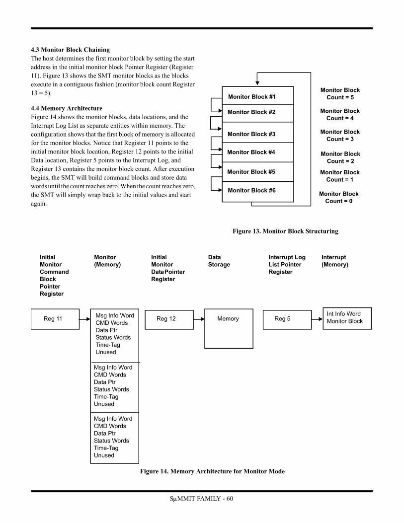
4.3 Monitor Block ChainingThe host determines the first monitor block by setting the start address in the initial monitor block Pointer Register (Register 11). Figure 13 shows the SMT monitor blocks as the blocks execute in a contiguous fashion (monitor block count Register 13 = 5).
4.4 Memory ArchitectureFigure 14 shows the monitor blocks, data locations, and the Interrupt Log List as separate entities within memory. The configuration shows that the first block of memory is allocated for the monitor blocks. Notice that Register 11 points to the initial monitor block location, Register 12 points to the initial Data location, Register 5 points to the Interrupt Log, and Register 13 contains the monitor block count. After execution begins, the SMT will build command blocks and store data words until the count reaches zero. When the count reaches zero, the SMT will simply wrap back to the initial values and start again.
Figure 14. Memory Architecture for Monitor Mode
Initial Monitor Command Block Pointer Register
Monitor(Memory)
DataStorage
Initial Monitor Data Pointer Register
Interrupt(Memory)
Msg Info WordCMD WordsData PtrStatus WordsTime-TagUnused
Reg 11 MemoryInt Info WordMonitor BlockReg 12
Interrupt Log List Pointer Register
Reg 5
Msg Info WordCMD WordsData PtrStatus WordsTime-TagUnused
Msg Info WordCMD WordsData PtrStatus WordsTime-TagUnused
Monitor Block #4
Monitor Block #1
Monitor Block #2
Monitor Block #3
Monitor Block #6
Monitor Block #5
Figure 13. Monitor Block Structuring
Monitor Block Count = 5
Monitor Block Count = 4
Monitor Block Count = 3
Monitor Block Count = 2
Monitor Block Count = 1
Monitor Block Count = 0
SMMIT FAMILY - 60

4.5 Message ProcessingTo process messages, the SMT uses data supplied in the internal registers along with external memory. The SMT uses eight external memory locations for each message called a monitor block. The monitor block is updated at the end of command processing. The following paragraphs discuss the monitor block in detail.
The SMMIT features two different modes of transferring data to RAM: Buffer and Non-Buffer. The user selects the Buffer or Non-Buffer transfer mode by setting the BUFR bit (bit 6) in the Control Register. See sections 9.1.5 or 9.2.3 for additional information.
The host or subsystem controlling the SMT allocates memory spaces for each monitor block. The top of the monitor blocks can reside at any address location. Initialized by the host, the SMT is linked to the monitor block via the initial monitor block Pointer Register and the Monitor Block Counter Register contents. Each monitor block contains a Message Information Word, Command Word 1, Command Word 2, Data Pointer, Status Word 1, Status Word 2, and Time-Tag. Refer to sections 4.2.1 - 4.2.6 for a full description of each location.
The Message Information word allows the SMT to tell the host or subsystem on which bus the command was received, whether the message was a RT-RT transfer, and conditions associated with the message. The SMT also stores each command word associated with the message into the appropriate location. For normal 1553 commands, only the first command word location will contain data. For RT-RT commands, the second command word location will contain data, and bit 8 in the Message Information word will be set.
For each command, the Data Pointer determines where to store data words. The SMT stores data sequentially from the top memory location. The SMT also stores each status word associated with the message into the appropriate location. For normal 1553 commands, only the first status word location will contain data. For RT-RT commands, the second status word location will contain data.The SMT begins monitoring after Control Register bit 15=1 (i.e., assertion of STEX).
After reception, the SMT begins post-processing. The SMT performs a DMA burst during post-processing. An optional interrupt log entry is performed after a monitor block is entered. Monitor Time-Out:
MIL-STD-1553A = 9sMIL-STD-1553B = 15s
See section 5, Enhanced SMMIT Family Operation for additional information.
4.5.1 Error Condition Message ProcessingWhen the monitor detects an error condition in either the command word, data words, or the RT’s status, the monitor block will not store the data. The monitor block counter increments. The initial message data pointer remains constant. The monitor block pointer increments. Message information bits of the monitor block are changed to reflect the error. An interrupt is given indicating a message has occurred. See section 4.2.1.1 for additional information.
4.6 Remote Terminal/Monitor Terminal OperationFor applications that require simultaneous Remote Terminal and Monitor Terminal operations, the SMMIT should be configured as both a remote terminal (SRT) and monitor terminal (SMT). This feature allows the SRT to communicate on the bus for one specific address and the SMT to monitor the bus for other specific addresses. Configuration as both SMT and SRT precludes the SMMIT from monitoring its own remote terminal address.
When the SMMIT is configured as both SRT and SMT, the SRT has priority over the SMT. For example, commands to the SRT will always take priority over monitoring functions for the SMT. The examples below describe what happens if the SRT is defined as terminal address 1 and the SMT is to monitor terminal address 12.
Example 1:
In this example, the SMT will decode the first command on bus A, realize the message is for terminal address 12, and start monitoring the message. However, as soon as the SRT realizes the second command on bus B is to terminal address 1, the SRT will take priority and begin SRT message processing.
Example 2:
Bus A
Bus B
CMD/TA =12
CMD/TA =1
Bus A
Bus B
CMD/TA =1
CMD/TA =12
SMMIT FAMILY - 61
In example 2, the SRT will decode the first command on bus A, realize the message is for terminal address 1, and start message processing. As the message on bus B is received, the SMMIT will realize it is to terminal address 12, but since the SRT has priority the SMT will not switch to the monitor mode.
The above examples also apply to a RT-RT message. For example, if the first command in a RT-RT transfer matches the terminal address of the SRT, the entire message will be processed by the SRT (Message 1). However, if the first command in a RT-RT transfer matches the terminal address of the SMT and the second command matches the terminal address of the SRT, the SRT will take priority and process the message (Message 2). Below is a RT-RT message example.
4.7 MIL-STD-1553A OperationTo maximize flexibility, the SMMIT has been designed to operate in many different systems which use various protocols. Specifically, two of the protocols that the SMMIT may be interfaced to are MIL-STD-1553A and MIL-STD-1553B. To meet these protocols, the SMMIT may be configured through an external pin or through control register bits (depending on the state of the LOCK pin).
Table 6. MIL-STD-1553A Operation
When configured as a MIL-STD-1553A monitor, the SMMIT will operate as follows:
Looks for the RT response within 9s (see section 5, Enhanced SMMIT Family Operation);
Defines all mode codes without data; Defines subaddress 00000 as a mode code.
Message 1
Message 2
CMD/TA =1
CMD/TA =12
CMD/TA =12
CMD/TA =1
A/B STD(pin)
RESULT
0 1553B response, 1553B standard
1 1553A response, 1553A standard
SMMIT FAMILY - 62

SµMMIT FAMILY - 63
5.0 ENHANCED SµMMIT FAMILY OPERATION
The following describes the Enhanced SµMMIT features.
5.1 Message Time-out Programmable bus controller and monitor time-out feature allows for the implementation of extended buses. Bit 9 of the Control Register determines the remote terminal no response time period. During MIL-STD-1553B operation, the program-mable time-out occurs at either 14µs or 30µs. In MIL-STD-1553A mode, time-out occurs at either 9µs or 21µs. See Figure 15.
5.2 DMA Time-outDMA time-out, in the bus controller mode of operation, is 16µS (tb, ta). The SµMMIT architecture times all DMA cycles to ensure that memory access timing supports message pro-cessing. Excessive memory access delays result in a DMA time-out condition. In the event of DMA time-out, the SµMMIT ceases message processing and generates an inter-rupt if enabled. The SµMMIT E and SµMMIT LXE/DXE specify the DMA time-out period per AC Electrical Character-istic tb. The SµMMIT XTE specifies the DMA time-out per AC Electrical Characteristic ta. See figure 38 for tb and figure 50 for ta.
5.3 Circular BuffersThe SµMMIT family circular buffer simplifies the software service of remote terminals implementing bulk or periodic data transfers. The Enhanced SµMMIT architecture allows the user to select one of two circular buffer modes. The user selects the preferred mode, at start-up, by writing to Control Register bits 7 and 8. The Control Register bits allow for the decode of three unique modes. Table 7 reviews mode selec-tions.
5.3.1 Mode Number 0Remote Terminal Index or Ping-Pong Operation, non-Enhanced SµMMIT, the user programs bits 7 and 8 to logical zero. Operation is per sections 2.2 and 2.3 (default state).
5.3.2 Mode Number 1 Remote Terminal Buffer 1, Enhanced SµMMIT operation, the user programs bit 7 to 0 and bit 8 to 1. The SµMMIT merges transmit or receive data into a circular buffer along with mes-sage information. For each valid receive message, the SµMMIT enters a message information word, time-tag word, and data word(s) into a unique receive circular buffer. For each valid transmit message, the SµMMIT enters a message infor-mation word and time-tag word into reserved memory loca-tions within the transmit circular buffer. The SµMMIT automatically controls the wrap around of circular buffers.
Two pointers define circular buffer length: top of buffer and bottom of buffer. User specifies the top of buffer (i.e., top address (TA16)) by writing a value into the second word of a unique mode code or subaddress descriptor block. The user defines the bottom of the buffer (i.e., bottom address (BA16)) by writing to the fourth word of that unique descriptor block. Both the TA16 and BA16 remain static during message process-
Control Register
Figure 15. Programmable Bus Controller Time-Out
Bit 9: Bus Controller and Monitor Only Time-OutLogical 0 time-out occurs at 14µsLogical 1 time-out occurs at 30µs
Table 1: Table 7. Enhanced Mode of Operation
Mode Number
Bit 7 Bit 8
0 0 0
1 0 1
X 1 0
2 1 1

SµMMIT FAMILY - 64
ing. The third word in the descriptor block identifies the cur-rent address (i.e., last accessed address plus one). The circular buffer wraps to the top address after completing a message that results in CA16 being greater than or equal to BA16. If CA16 increments past BA16 during intra-message processing, the SµMMIT will access memory (read or write) address locations past BA16. Delimit all circular buffer boundaries with at least 34 address locations.
Each subaddress and mode code, both transmit and receive, has a unique circular buffer assignment. The SµMMIT decodes the command word T/R bit, subaddress/mode field, and word count/mode code field to select a unique descriptor block which contains TA16, CA16, and BA16.
For receive messages, the SµMMIT stores the message infor-mation word into address location CA16, the time-tag word into CA16+ 116, and the data into the next “N16” locations starting at address CA16+216. For each transmit command, the SµMMIT stores the message information word into address location CA16 and time-tag word into location CA16+ 116. Retrieval of data for transmission starts at address location CA16 + 216. When entering multiple transmit command data packets into the circular buffer, delimit each data packet with two reserved memory locations. The SµMMIT enters the mes-sage information word and time-tag word into the delimiting memory locations.
5.3.3 Mode Number 2 Circular Buffer 2, enhanced SµMMIT operation, the user pro-grams Control Register bit 7 to 1 and bit 8 to 1. The SµMMIT separates message data and message information into unique circular buffers. The separation of data from message informa-tion simplifies the software that loads and unloads data from the buffers. Each subaddress and mode code, both transmit and receive, has a unique pair of circular buffers. The SµMMIT decodes the command word T/R bit, subaddress/mode field, and word count/mode code field to select a unique descriptor block which contains TA16, CA16, and Message Information Buffer (MIB).
Control the wrap-around of both the data and message circular by specifying the number of messages before wrap-around occurs. The second word entered into the descriptor block determines the top of the data buffer (TA16). The third word in the descriptor block identifies the current position (CA16) in the buffer (i.e., last accessed address plus one). The fourth word in the descriptor block identifies the MIB’s starting loca-tion and current position. The MIB contains Time-Tag and Message Information words for each message transacted on the bus. The data buffer and message information word buffer wrap around after processing a pre-determined number of
messages. Each subaddress and mode code, both transmit and receive, has a unique data buffer and MIB assignment.
5.4 Ping-Pong HandshakeThe Enhanced SµMMIT provides a software handshake which indicates the enable and disable of buffer ping-pong operation. During remote terminal operation, the SµMMIT asynchronous ping-pongs between two subaddress or mode code data buff-ers. To perform buffer service, the application software must freeze the remote terminal’s access to a single buffer. The SµMMIT’s ping-pong enable/disable handshake allows the application software to asynchronously freeze (i.e., disable ping-pong operation) the remote terminal to a single buffer.
5.5 Circular Buffer Mode #1To implement Circular Buffer 1’s architecture, the four word descriptor block and Control Register are different than in the mode #0. Bits 15 through 8 of the Control Word are don’t care. The second word of the descriptor block defines the buffer’s starting or top address (TA16). The TA pointer remains static during message processing. The fourth entry into the descrip-tor block identifies the buffer’s bottom address (i.e., BA16) and also remains static during message processing. The third descriptor block word represents the current address (i.e., CA16) in the buffer and is dynamic. If the SµMMIT observes no message error conditions, the CA16 pointer updates at the end of message processing. The application software reads the dynamic CA16 pointer to determine the current bottom of the buffer.
First, a review of receive message processing. The SµMMIT begins all message processing by reading a unique descriptor block after reception and validation of a subaddress or mode code command word. The SµMMIT internally increments the CA16 pointer to store the receive data word(s). After message processing completes, the SµMMIT stores the message infor-mation word and time-tag word into the circular buffer preced-ing the message data. At the end of message processing, the SµMMIT updates CA16 (if no errors detected). For CA16 larger than BA16 storage of the next message begins at the address location pointed to by the TA16 pointer, and CA16 is made equal to TA16. If CA16 is less than BA16 , CA16 points to the next available memory location in the buffer (i.e., CA16 + 1).
For transmit commands, the SµMMIT begins transmission of data from memory location CA16 + 216. Reserve the first two locations for the message information word and time-tag word. After message processing completes, the SµMMIT enters the message information word and time-tag word into the circular buffer. At the end of message processing, the SµMMIT updates CA16 (if no errors detected). For CA16

SµMMIT FAMILY - 65
larger than BA16, storage of the next message begins at the address location pointed to by the TA16 pointer, and CA16 is made to equal TA16. If CA16 is less than BA16, CA16 points to the next available memory location in the buffer (i.e. CA16 + 1).
In this mode of operation, bits INDX, NII and A/B of the Descriptor Control Word and the PPEN bit of the Control Reg-ister are don’t care. Message information word bit 5 reflects the reception of broadcast message via the BRD bit.
The SµMMIT generates a circular buffer empty/full interrupt when the buffer reaches the end (i.e., CA16 greater than BA16) and begins a new message at the top of the buffer. Bit 8 of the Mask Register and bit 7 of the Descriptor Control Word mask enables the generation of the Full/Empty interrupt. On the occurrence of either interrupt, the MSG_INT output asserts. Figure 16 describes the relationship between TA16, BA16, and CA16.
Control Register
Descriptor BlockControl Word
TA
CA
BA
Circular Buffer
Time-Tag
Data Words
Message Information Word
Bits 7 and 8 Select Circular Buffer
Data Words
Data Words
Figure 16. Circular Buffer Mode #1
Message Information Word
Time-Tag
Data Words
Data Words
SµMMIT FAMILY - 66
5.6 Circular Buffer Mode #2To implement Circular Buffer 2’s architecture, the descriptor block and Control Register are different than in mode #0. Bits 15 through 8 of the Control Word spec-ify the Message Information Buffer (MIB) length; the maximum MIB length is 256. Table 8 shows how the Control Word’s most significant bits select the depth of the MIB. The Control Words eight most significant bits remain static during message processing.
The second word of the descriptor block defines the top address (TA16) of the data circular buffer. The TA16 pointer remains static during message processing. The third descriptor word identifies the current address (i.e., CA16) of the data circular buffer. The application soft-ware reads the dynamic CA16 pointer to determine the current address of the data buffer. The SµMMIT incre-ments the CA16 pointer, at the end of message process-ing, until the MIB buffer is full. When the MIB wraps around, the SµMMIT loads the CA16 pointer with the TA16 pointer.
The fourth word in the descriptor block defines the top or base address of the Message Information Buffer (i.e., MIB) and the current MIB address (i.e., offset from base address). The SµMMIT enters the message information word and time-tag word into the MIB, for each message, until the end of the MIB is reached. When the MIB reaches the end, the next message’s message informa-tion word and time-tag word is entered at the top of the MIB. The MIB pointer is a semi-static pointer. The SµMMIT updates the current address field at the end of message processing. The base address field remains static.
Application software reads the current MIB address to determine the number of messages processed since last service. The variable length MIB requires the base address and current address field to also vary in length. Table 8 displays the relationship between Control Word bits 15 through 8, MIB length, MIB base and current address fields. The current address field of the MIB must begin on an even boundary.
First is a review of receive message processing. The SµMMIT begins all message processing by reading the descriptor block of the subaddress or mode code com-mand received (i.e., ControlWord, TA16, CA16, and MIB). The SµMMIT begins storage of data word(s) starting at the location contained in the CA16 pointer.
The SµMMIT automatically updates the CA16 pointer internally as message processing progresses. After receiving the correct number of data words, the SµMMIT stores the message information word and time-tag word into the MIB. At the end of message pro-cessing, the SµMMIT updates CA16 and MIB Current Address Field (CAF). If CAF equals the specified MIB length, CA16 is updated to TA16 and the MIB CAF is reset to zero. If CAF is less than the specified MIB length, CA16 and MIB CAF point to the next available memory location in each buffer. Control Word bits 15 to 8 specify the MIB length.
For transmit commands, the SµMMIT begins transmis-sion of data from memory location CA16. After message processing completes, the SµMMIT enters the message information word and time-tag word into the MIB. At the end of message processing, the SµMMIT updates CA16 and the MIB CAF. If CAF equals the specified MIB length, CA16 is updated to TA16 and the MIB CAF is reset to zero. If CAF is less than the specified MIB length, CA16 and MIB CAF point to the next available memory location in each buffer.
In this mode of operation, bits INDX, NII and A/B of the descriptor control word and the PPEN bit of the Command Register are don’t care. The BRD bit is added to the Message Information Word bit 5.
The SµMMIT generates a circular buffer empty/full interrupt when the MIB reaches the end and begins a new message at the top of the buffer. Bit 8 of the Mask Register and bit 7 of the descriptor Control Word mask and enable the generation of the Full/Empty interrupt. On the occurrence of either interrupt, the MSG_INT output asserts. Figure 17 describes the relationship between TA16, CA16, and MIB.
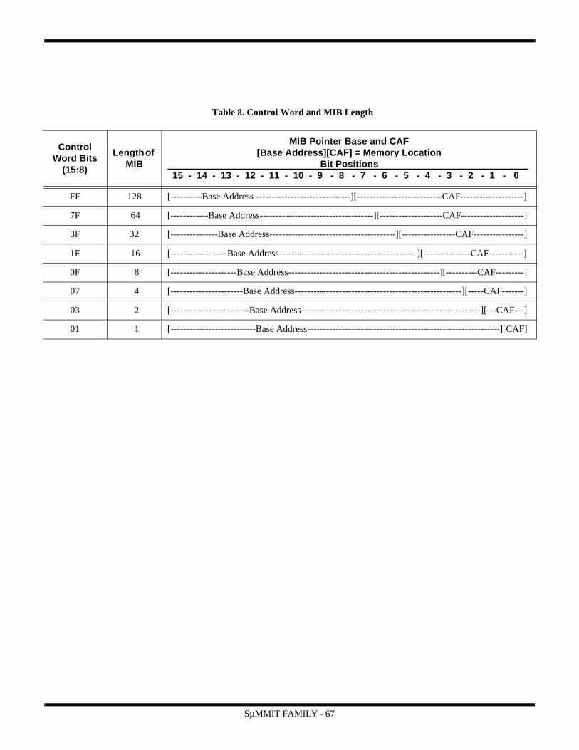
SµMMIT FAMILY - 67
Table 8. Control Word and MIB Length
Control Word Bits
(15:8)
Length of MIB
MIB Pointer Base and CAF[Base Address][CAF] = Memory Location
Bit Positions 15 - 14 - 13 - 12 - 11 - 10 - 9 - 8 - 7 - 6 - 5 - 4 - 3 - 2 - 1 - 0
FF 128 [----------Base Address ------------------------------][---------------------------CAF--------------------]
7F 64 [------------Base Address------------------------------------][--------------------CAF--------------------]
3F 32 [---------------Base Address----------------------------------------][-----------------CAF----------------]
1F 16 [------------------Base Address------------------------------------------- ][---------------CAF-----------]
0F 8 [---------------------Base Address------------------------------------------------][----------CAF---------]
07 4 [-----------------------Base Address-----------------------------------------------------][-----CAF-------]
03 2 [-------------------------Base Address---------------------------------------------------------][---CAF---]
01 1 [---------------------------Base Address-------------------------------------------------------------][CAF]
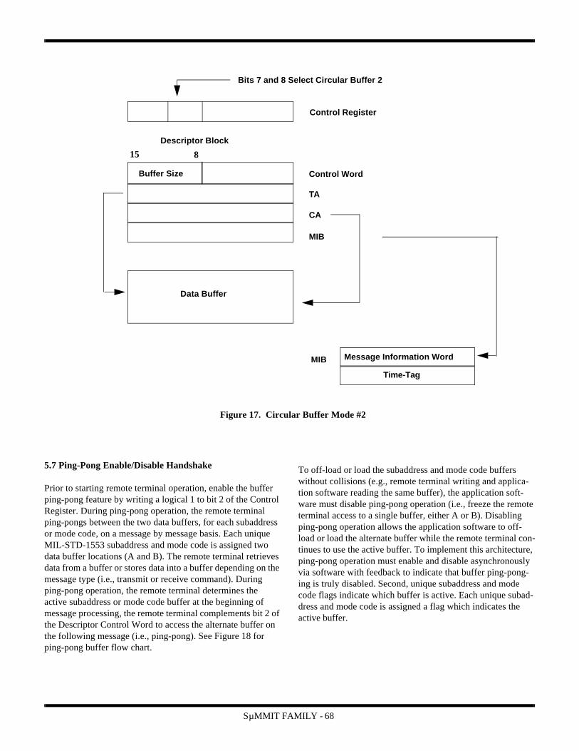
SµMMIT FAMILY - 68
5.7 Ping-Pong Enable/Disable Handshake
Prior to starting remote terminal operation, enable the buffer ping-pong feature by writing a logical 1 to bit 2 of the Control Register. During ping-pong operation, the remote terminal ping-pongs between the two data buffers, for each subaddress or mode code, on a message by message basis. Each unique MIL-STD-1553 subaddress and mode code is assigned two data buffer locations (A and B). The remote terminal retrieves data from a buffer or stores data into a buffer depending on the message type (i.e., transmit or receive command). During ping-pong operation, the remote terminal determines the active subaddress or mode code buffer at the beginning of message processing, the remote terminal complements bit 2 of the Descriptor Control Word to access the alternate buffer on the following message (i.e., ping-pong). See Figure 18 for ping-pong buffer flow chart.
To off-load or load the subaddress and mode code buffers without collisions (e.g., remote terminal writing and applica-tion software reading the same buffer), the application soft-ware must disable ping-pong operation (i.e., freeze the remote terminal access to a single buffer, either A or B). Disabling ping-pong operation allows the application software to off-load or load the alternate buffer while the remote terminal con-tinues to use the active buffer. To implement this architecture, ping-pong operation must enable and disable asynchronously via software with feedback to indicate that buffer ping-pong-ing is truly disabled. Second, unique subaddress and mode code flags indicate which buffer is active. Each unique subad-dress and mode code is assigned a flag which indicates the active buffer.
Bits 7 and 8 Select Circular Buffer 2
Control Register
Descriptor Block
15 8
Buffer Size Control Word
TA
CA
MIB
Data Buffer
Message Information Word
Time-Tag
Figure 17. Circular Buffer Mode #2
MIB
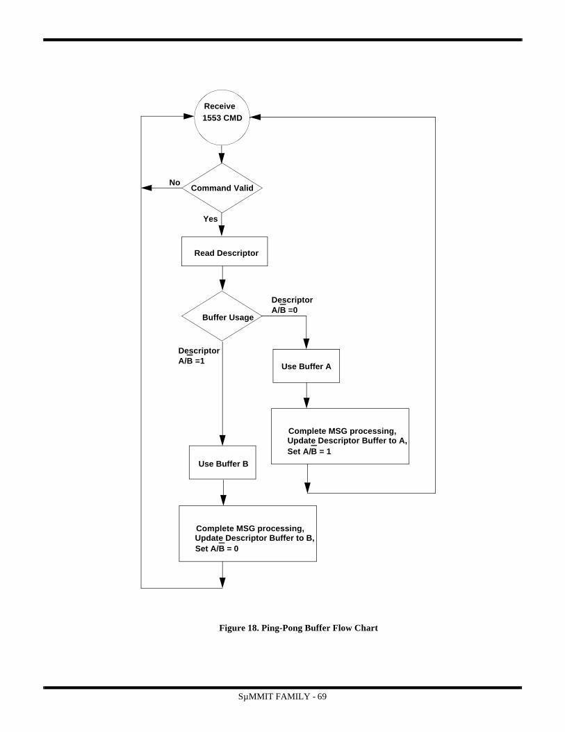
SµMMIT FAMILY - 69
Use Buffer B
Buffer Usage
Descriptor
Use Buffer A
Read Descriptor
Complete MSG processing,Update Descriptor Buffer to A,
A/B =0
Descriptor A/B =1
Set A/B = 1
Complete MSG processing,Update Descriptor Buffer to B,Set A/B = 0
Receive1553 CMD
Command Valid
Yes
No
Figure 18. Ping-Pong Buffer Flow Chart

SµMMIT FAMILY - 70
To begin the process of off-loading or loading the remote ter-minal’s subaddress and/or mode code buffers, when using the ping-pong feature, the application software performs the fol-lowing sequence: disables ping-pong operation, determines the active buffer, services the alternate buffer, enables ping-pong operation.
The application software disables ping-pong operation by writing a logical zero to Control Register bit 2. The disable of ping-pong operation is acknowledged by bit 9 of the Control Register. Bit 9 of the Control Register acknowledges the ping-pong disable by transitioning from a logical one to a logical zero. The application software interrogates bit 2 of each Descriptor Control Word to determine the active buffer on a subaddress or mode code basis. If bit 2 is a logical zero, the remote terminal uses Buffer A and the application software off-loads or loads Buffer B. If bit 2 is a logical one, the remote terminal uses Buffer B and the application software off-loads or loads Buffer A. Figure 19 displays Control Register bits for ping-pong enable/disable and acknowledge.
The application software enables ping-pong operation by writ-ing a logical one to Control Register bit 2. The enable of ping-pong operation is acknowledged by bit 9 of the Control Regis-ter. Bit 9 of the Control Register acknowledges the ping-pong enable by transitioning from a logical zero to a logical one.
15 9 2 0
Logical 0Ping-Pong
Logical 1Ping-Pong
Figure 19. Ping-Pong Handshake
Enabled Disabled
Control Register
Enable/Disable AcknowledgeLogical 0: Disable AcknowledgeLogical 1: Enable Acknowledge
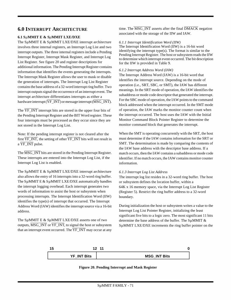
SµMMIT FAMILY - 71
6.0 INTERRUPT ARCHITECTURE
6.1 SµMMIT E & SµMMIT LXE/DXEThe SµMMIT E & SµMMIT LXE/DXE interrupt architecture involves three internal registers, an Interrupt Log List and two interrupt outputs. The three internal registers include a Pending Interrupt Register, Interrupt Mask Register, and Interrupt Log List Register. See figure 20 and register descriptions for additional information. The Pending Interrupt Register contains information that identifies the events generating the interrupts. The Interrupt Mask Register allows the user to mask or disable the generation of interrupts. The Interrupt Log List Register contains the base address of a 32-word interrupt ring buffer. Two interrupt outputs signal the occurrence of an interrupt event. The interrupt architecture differentiates interrupts as either a hardware interrupt (YF_INT) or message interrupt (MSG_INT).
The YF_INT interrupt bits are stored in the upper four bits of the Pending Interrupt Register and the BIT Word register. These four interrupts must be processed as they occur since they are not stored in the Interrupt Log List.
Note: If the pending interrupt register is not cleared after the first YF_INT, the setting of other YF_INT bits will not result in a YF_INT pulse.
The MSG_INT bits are stored in the Pending Interrupt Register. These interrupts are entered into the Interrupt Log List, if the Interrupt Log List is enabled.
The SµMMIT E & SµMMIT LXE/DXE interrupt architecture also allows the entry of 16 interrupts into a 32-word ring buffer. The SµMMIT E & SµMMIT LXE/DXE automatically handles the interrupt logging overhead. Each interrupt generates two words of information to assist the host or subsystem when processing interrupts. The Interrupt Identification Word (IIW) identifies the type(s) of interrupt that occurred. The Interrupt Address Word (IAW) identifies the interrupt source via a 16-bit address.
The SµMMIT E & SµMMIT LXE/DXE asserts one of two outputs, MSG_INT or YF_INT, to signal the host or subsystem that an interrupt event occurred. The YF_INT may occur at any
time. The MSG_INT asserts after the final DMACK negation associated with the storage of the IIW and IAW.
6.1.1 Interrupt Identification Word (IIW)The Interrupt Identification Word (IIW) is a 16-bit word identifying the interrupt type(s). The format is similar to the Pending Interrupt Register. The host or subsystem reads the IIW to determine which interrupt event occurred. The bit description for the IIW is provided in Table 9.
6.1.2 Interrupt Address Word (IAW)The Interrupt Address Word (IAW) is a 16-bit word that identifies the interrupt source. Depending on the mode of operation (i.e., SRT, SBC, or SMT), the IAW has different meanings. In the SRT mode of operation, the IAW identifies the subaddress or mode code descriptor that generated the interrupt. For the SBC mode of operation, the IAW points to the command block addressed when the interrupt occurred. In the SMT mode of operation, the IAW marks the monitor counter count when the interrupt occurred. The host uses the IAW with the Initial Monitor Command Block Pointer Register to determine the monitor command block that generates the interrupt.
When the SMT is operating concurrently with the SRT, the host must determine if the IAW contains information for the SRT or SMT. The determination is made by comparing the contents of the IAW base address with the descriptor base address. If a match occurs, then the IAW contains a subaddress or mode code identifier. If no match occurs, the IAW contains monitor counter information.
6.1.3 Interrupt Log List AddressThe interrupt log list resides in a 32-word ring buffer. The host or subsystem defines the location buffer, within a 64K x 16 memory space, via the Interrupt Log List Register (Register 5). Restrict the ring buffer address to a 32-word boundary.
During initialization the host or subsystem writes a value to the Interrupt Log List Pointer Register, initializing the least significant five bits to a logic zero. The most significant 11 bits determine the base address of the buffer. The SµΜΜIT & SµΜΜIT LXE/DXE increments the ring buffer pointer on the
Figure 20. Pending Interrupt and Mask Register
15 12 11
YF_INT Bits MSG_INT Bits
0

SµMMIT FAMILY - 72
occurrence of the first interrupt, storing the IIW and IAW at locations 00000 and 00001 respectively. The SµΜΜIT E & SµΜΜIT LXE/DXE logs ensuing interrupts sequentially into the ring buffer until interrupt number 16 occurs. The SµΜΜIT E & SµΜΜIT LXE/DXE enters interrupt 16’s IIW in buffer location 11110 and the IAW at location 11111. The ring wraps-around at a value of 11111.
The SµΜΜIT E & SµΜΜIT LXE/DXE increments the ring buffer pointer as interrupts occur. The least significant five bits of the Interrupt Log List Pointer Register reflect the ring buffer pointer value. Figure 21 shows the ring buffer architecture.
The host or subsystem reads the ring buffer pointer value to determine the number of interrupts that have occurred. By extracting the least significant five bits from the Interrupt Log List Register and logically shifting the data once to the right, the host or subsystem determines the number of interrupt events.
Table 9. Interrupt Information Word
BitNumber
Mnemonic Description
15-12 N/A Not Applicable.
11 MERR Message Error Interrupt (All modes).
10 SUBAD Subaddress Accessed Interrupt (SRT).
9 BDRCV Broadcast Command Received Interrupt (SRT).
8 IXEQ0 Index Equal Zero Interrupt (SRT).
7 ILCMD Illegal Command Interrupt (SRT).
6 N/A Not Applicable.
5 EOL End of List (SBC).
4 ILLCMD Illogical Command (SBC).
3 ILLOP Illogical Opcode (SBC).
2 RTF Retry Fail (SBC).
1 CBA Command Block Accessed (SBC).
0 MBC Monitor Block Count Equal Zero (SMT).

SµMMIT FAMILY - 73
Figure 21. Interrupt Ring Buffer
Base Address + 00000
Base Address + 00001
Base Address + 00010
Base Address + 00011
Base Address + 00100
Base Address + 00101
Base Address + 00110
Base Address + 00111
Base Address + 01000
Base Address + 01001
Base Address + 01010
Base Address + 01011
Base Address + 01100
Base Address + 01101
Base Address + 01110
Base Address + 01111
Base Address + 10000
Base Address + 10001
Base Address + 10010
Base Address + 10011
Base Address + 10100
Base Address + 10101
Base Address + 10110
Base Address + 10111
Base Address + 11000
Base Address + 11001
Base Address + 11010
Base Address + 11011
Base Address + 11100
Base Address + 11101
Base Address + 11110
Base Address + 11111
IIW #1
IIW #2
IIW #3
IIW #4
IIW #5
IIW #6
IIW #7
IIW #8
IIW #9
IIW #10
IIW #11
IIW #12
IIW #13
IIW #14
IIW #15
IIW #16
IAW #16
IAW #1
IAW #2
IAW #3
IAW #4
IAW #5
IAW #6
IAW #7
IAW #8
IAW #9
IAW #10
IAW #11
IAW #12
IAW #13
IAW #14
IAW #15
Interrupt Log ListAddress Register Contents
Interrupt Log ListAddress Register Contents
Ring-Buffer Pointer
SµMMIT FAMILY - 74
6.2 SµMMIT XTEThe SµMMIT XTE’s interrupt architecture involves three internal registers, an Interrupt Log List, two interrupt outputs, and two interrupt acknowledges. The three internal registers include a Pending Interrupt Register, Interrupt Mask Register, and Interrupt Log List Register. See figure 20 and register descriptions for additional information. The Pending Interrupt Register contains information that identifies the events generating the interrupts. The Interrupt Mask Register allows the user to mask or disable the generation of interrupts. The Interrupt Log List Register contains the base address of a 32-word interrupt ring buffer. Two interrupt outputs signal the occurrence of an interrupt event. The interrupt architecture differentiates interrupts as either a hardware interrupt (YF_INT) or message interrupt (MSG_INT). The user programs the interrupt outputs as either pulsed outputs or level outputs depending on system requirements.
Assertion of the YF_INT interrupt signals a hardware failure condition. Failures include DMA time-out, wrap-around self-test, terminal address parity, or built-in test (BIT). YF_INT failures are reflected in the four most significant bits of the Pending Interrupt Register. The YF_INT output asserts on the occurrence of a failure.
Assertion of the MSG_INT interrupt signals a message related event has occurred. MSG_INT events are reflected in the 12 least significant bits of the Pending Interrupt Register. The MSG_INT asserts after message processing is complete.
The interrupt architecture allows for the entry of 16 interrupts into a 32-word ring buffer (see figure 21). The SµMMIT XTE automatically handles the interrupt logging overhead. Each interrupt generates two words of information to help the host or subsystem perform interrupt processing. The Interrupt Identification Word (IIW) identifies the type(s) of interrupt that occurred. The Interrupt Address Word (IAW) identifies the interrupt source (e.g., subaddress or command block) via a 16-bit address.
The SµMMIT XTE’s interrupt outputs are user programmable. The user can select either pulsed interrupt outputs or level sensitive outputs. In the level mode of operation, assertion of either input (i.e., YF_ACK or MSG_ACK) negates the respective interrupt output (i.e., YF_INT or MSG_INT). The state of MSEL(4) selects the mode of operation, Table 10 reviews operation.
Table 10. MSEL(4) Operation
6.2.1 Interrupt Identification Word (IIW)The Interrupt Identification Word (IIW) is a 16-bit word identifying the interrupt type(s). The format is similar to the Pending Interrupt Register. The host or subsystem reads the IIW to determine which interrupt event occurred. The bit descriptor for the IIW is provided in Table 9.
6.2.2 Interrupt Address Word (IAW)The Interrupt Address Word (IAW) is a 16-bit word that identifies the interrupt source. Depending on the mode of operation (i.e., SRT, SBC, or SMT), the IAW has different meanings. In the SRT mode of operation, the IAW identifies the subaddress or mode code descriptor that generated the interrupt. For the SBC mode of operation, the IAW points to the command block addressed when the interrupt occurred. In the SMT mode of operation, the IAW marks the monitor counter count when the interrupt occurred. The host uses the IAW with the Initial Monitor Command Block Pointer Register to determine the monitor command block that generates the interrupt.
When the SMT is operating concurrently with the SRT, the host must determine if the IAW contains information for the SRT or SMT. The determination is made by comparing the contents of the IAW base address with the descriptor base address. If a match occurs, then the IAW contains a subaddress or mode code identifier. If no match occurs, the IAW contains monitor counter information.
6.2.3 Interrupt Log List AddressThe interrupt log list resides in a 32-word ring buffer. The host or subsystem defines the location buffer, within a 32K x 16 memory space, via the Interrupt Log List Register (Register 5). Restrict the ring buffer address to a 32-word boundary.
MSEL(4) YF_INT
MSG_INT
YF_ACK
MSG_ACK
0 Pulse Output Tied High
1 Level Output Active Low
SµMMIT FAMILY - 75
During initialization the host or subsystem writes a value to the Interrupt Log List Pointer Register, initializing the least significant five bits to a logic zero. The most significant 11 bits determines the base address of the buffer. The SµMMIT XTE increments the ring buffer pointer on the occurrence of the first interrupt, storing the IIW and IAW at locations 00000 and 00001 respectively. The SµMMIT XTE logs ensuing interrupts sequentially into the ring buffer until interrupt number 16 occurs. The SµMMIT XTE enters interrupt 16’s IIW in buffer location 11110 and the IAW at location 11111. The ring wraps-around at a value of 11111.
The SµMMIT XTE increments the ring buffer pointer as interrupts occur. The least significant five bits of the Interrupt Log List Pointer Register reflect the ring buffer pointer value. Figure 21 shows the ring buffer architecture.
The host or subsystem reads the ring buffer pointer value to determine the number of interrupts that have occurred. By extracting the least significant five bits from the Interrupt Log List Register and logically shifting the data once to the right, the host or subsystem determines the number of interrupt events.

SµMMIT FAMILY - 76
7.0 AUTO-INITIALIZATION
7.1 SµMMIT E & SµMMIT LXE/DXEThe SµMMIT E & SµMMIT LXE/DXE auto-initialization feature allows autonomous operation. The SµMMIT E & SµMMIT LXE/DXE will automatically configure itself for operation from nonvolatile 16-bit wide memory (PROM, ROM,
E2PROM, EPROM, etc.). The configuration sequence begins after the negation of input pin MRST, if AUTOEN is enabled. For each mode of operation, the auto-initialization function is different. The following section outlines the auto-initialization feature for each mode of operation.
7.1.1 SRT Auto-InitializationDuring auto-initialization, the SµMMIT E & SµMMIT LXE/DXE loads all internal registers and transfers the descriptor space into RAM. Initialize registers not used during SRT operation to 0000 (hex). The SRT must have 32 memory locations allocated for register data.
Following register initialization, the SµMMIT E & SµMMIT LXE/DXE reads the descriptor from ROM and enters the descriptor into RAM. The starting address for the descriptor is read from the Descriptor Pointer Register. The SµMMIT E & SµMMIT LXE/DXE internally generates all address information required for auto-initialization.
The SµMMIT E & SµMMIT LXE /DXE requires 544 consecutive ROM locations for initialization. The 544 memory locations include: 32 for internal register information, 256 for subaddress descriptor information, and 256 for mode code descriptor information. Unused descriptor blocks should be initialized to four words of 0000 (hex).
The SRT accesses 544 consecutive memory locations in 32-word blocks. The SRT arbitrates for the bus once. Once access is granted, the SRT reads 32 words from ROM, then transfers the information into RAM. The SRT does not release the bus until all 544 ROM locations are transferred. The SRT does not respond to MIL-STD-1553 commands until initialization is complete, the start execution bit has been set, and the RT parity has been verified. After initialization, the SRT can respond to MIL-STD-1553 commands.
7.1.2 SMT Auto-InitializationSMT auto-initialization requires only the loading of internal registers. Registers not used during SMT operation should be initialized to 0000 (hex). The SMT requires allocation of 32 memory locations for register data. The SµMMIT E & SµMMIT
LXE/DXE internally generates all address information for auto-initialization.
When operating as a concurrent SRT and SMT, the SµMMIT E & SµMMIT LXE/DXE loads all internal registers for both SRT and SMT modes of operation. The device then transfers the descriptor from ROM to RAM.
7.1.3 SBC Auto-InitializationDuring auto-initialization the SµMMIT E & SµMMIT LXE/DXE loads all internal registers and transfers the command block(s) into RAM. Registers not used during SBC operation should be initialized to 0000 (hex). The SBC requires the allocation of 32 memory locations for register data.
Following register initialization, the SµMMIT E & SµMMIT LXE/DXE reads command block(s) information from ROM and enters them into RAM. The starting address for the command block(s) is read from the Command Block Pointer Register. The SµMMIT E & SµMMIT LXE/DXE internally generates all address information for auto-initialization.
The SBC continues to read command blocks from ROM until the Command Block Initialization Count Register decrements to zero.
7.1.4 Auto-Initialization HardwareTo enable the auto-initialization function, assert the AUTOEN pin before the rising edge of MRST. The de-assertion of MRST signals the beginning of the auto-initialization sequence. The assertion of output ROMEN enables the ROM for data access. Output ROMEN remains active until the completion of auto-initialization. Simultaneous with the assertion of ROMEN, the SµMMIT E & SµMMIT LXE/DXE arbitrates for the bus by asserting DMAR. Upon completion of auto-initialization, the SµMMIT E & SµMMIT LXE/DXE asserts the READY output pin. Output READY asserts after negation of DMACK. At this time, the SµMMIT E & SµMMIT LXE/DXE is prepared for operation, if it has been started (i.e., STEX=1). The SµMMIT E & SµMMIT LXE/DXE is idle until reception of a valid command word, or begins command block processing.
The ROM’s starting location is 0000 (hex), RAM and ROM are overlaid by using the ROMEN output pin as a ROM device select or output enable. Figures 22a and 22b show examples of the relative timing associated with an auto-initialization sequence.

SµMMIT FAMILY - 77
MRST
AUTOEN
ROMEN
DMAACTIVITY
READY
MRST
AUTOEN
RTA(4:0)
RTPTY
LOCK
10ns (min)5.0µs (min)
Note:1. UTMC strongly recommends that these inputs remain static until the assertion of READY.
VALID
VALID
VALID
VALID
ROMEN 5.0µs (max)
DMAR
VALIDA/B STD andMSEL(1:0)
5.0µs (max)
Figure 22a. Auto-Initialization Timing
Figure 22b. Auto-Initialization DMA Sequence

SµMMIT FAMILY - 78
7.2 SµMMIT XTEThe SµMMIT XTE auto-initialization feature allows autonomous operation. The SµMMIT XTE will automatically configure itself for operation from nonvolatile byte-wide
memory (PROM, ROM, E2PROM, EPPROM, etc.). The configuration sequence begins after the negation of input pin MRST, if AUTOEN is enabled. For each mode of operation, the auto-initialization function is different. The following sections outline the auto-initialization feature for each mode of operation.
7.2.1 SRT Auto-InitializationDuring auto-initialization, the SµMMIT XTE loads all internal registers and transfers the descriptor space into RAM. Initialize registers not used during SRT operation to 0000 (hex). The SRT must have 64 memory locations allocated for register data.
Following register initialization, the SµMMIT XTE reads the descriptor from ROM and enters the descriptor into RAM. The starting address for the descriptor is read from the Descriptor Pointer Register. The SµMMIT XTE internally generates all address information required for auto-initialization.
The SµMMIT XTE requires 1088 consecutive ROM locations for initialization. The 1088 memory locations include: 64 for internal register information, 512 for subaddress descriptor information, and 512 for mode code descriptor information. Unused descriptor blocks should be initialized to four words of 0000 (hex).
The SRT accesses 1088 consecutive memory locations in 64-word blocks. Once access is granted, the SRT reads words from ROM, then transfers the information into RAM. The SRT does not respond to MIL-STD-1553 commands until initialization is complete, the start execution bit has been set, and the RT parity has been verified. After initialization, the SRT can respond to MIL-STD-1553 commands.
7.2.2 SMT Auto-InitializationSMT auto-initialization requires only the loading of internal registers. Registers not used during SMT operation should be initialized to 0000 (hex). The SMT requires allocation of 64 memory locations for register data. The SµMMIT XTE internally generates all address information for auto-initialization.
When operating as a concurrent SRT and SMT, the SµMMIT XTE loads all internal registers for both SRT and SMT modes of operation. The device then transfers the descriptor from ROM to RAM.
7.2.3 SBC Auto-InitializationDuring auto-initialization the SµMMIT XTE loads all internal registers and transfers the command block(s) into RAM. Registers not used during SBC operation should be initialized to 0000 (hex). The SBC requires the allocation of 64 memory locations for register data.
Following register initialization, the SµMMIT XTE reads command block(s) information from ROM and enters them into RAM. The starting address for the command block(s) is read from the Command Block Pointer Register. The SµMMIT XTE internally generates all address information for auto-initialization.
The SBC continues to read command blocks from ROM until the Command Block Initialization Count Register decrements to zero.
7.2.4 Auto-Initialization HardwareAn external auto-initialization bus allows configuration of SµMMIT XTE without host intervention. Auto-initialization is ideal for low cost remote sensing applications where a host microprocessor or microcontroller is not required.
To enable the auto-initialization function, assert the AUTOEN pin prior to the rising edge of MRST. The assertion of MRST signals the beginning of the auto-initialization sequence. The SµMMIT XTE enables the boot memory by asserting the ECS output. The SµMMIT XTE accesses up to 8K x 8 words via the auto-initialization bus. Table 8 reviews the memory requirements for SµMMIT XTE auto-initialization.
Table 11. Auto-Initialization Memory Requirements
Note:1. N equals the number of command blocks.
Mode Memory (x8)
SRT 1088
SMT 64
SBC 64 + [N x (16)] 1
SµMMIT FAMILY - 79
To interface to slower non-volatile memory the auto-initialization read cycle period is programmable. The user selects between zero and seven wait states per read. A wait state is equal to 82ns. The user programs the read cycle duration via inputs EC(2:0). The SµMMIT XTE latches inputs EC(2:0) on the rising edge of MRST. Table 12 reviews the possible combinations of wait-states. Figures 23a and 23b show a system configuration along with typical auto-initialization read cycles. Following completion of an auto-initialization sequence the SµMMIT XTE asserts the READY output.
Table 12. Programmable Wait-State
EC(2:0)2 Number of Wait-States
000 0
001 1
010 2
011 3
100 4
101 5
110 6
111 7
Figure 23a. Auto-Initialization System Configuration
SµMMIT XTE
AUTOEN
ECS
ED(7:0)
EA(12:0)
AUTO-INITMEMORY
A(12:0)
D(7:0)
CS
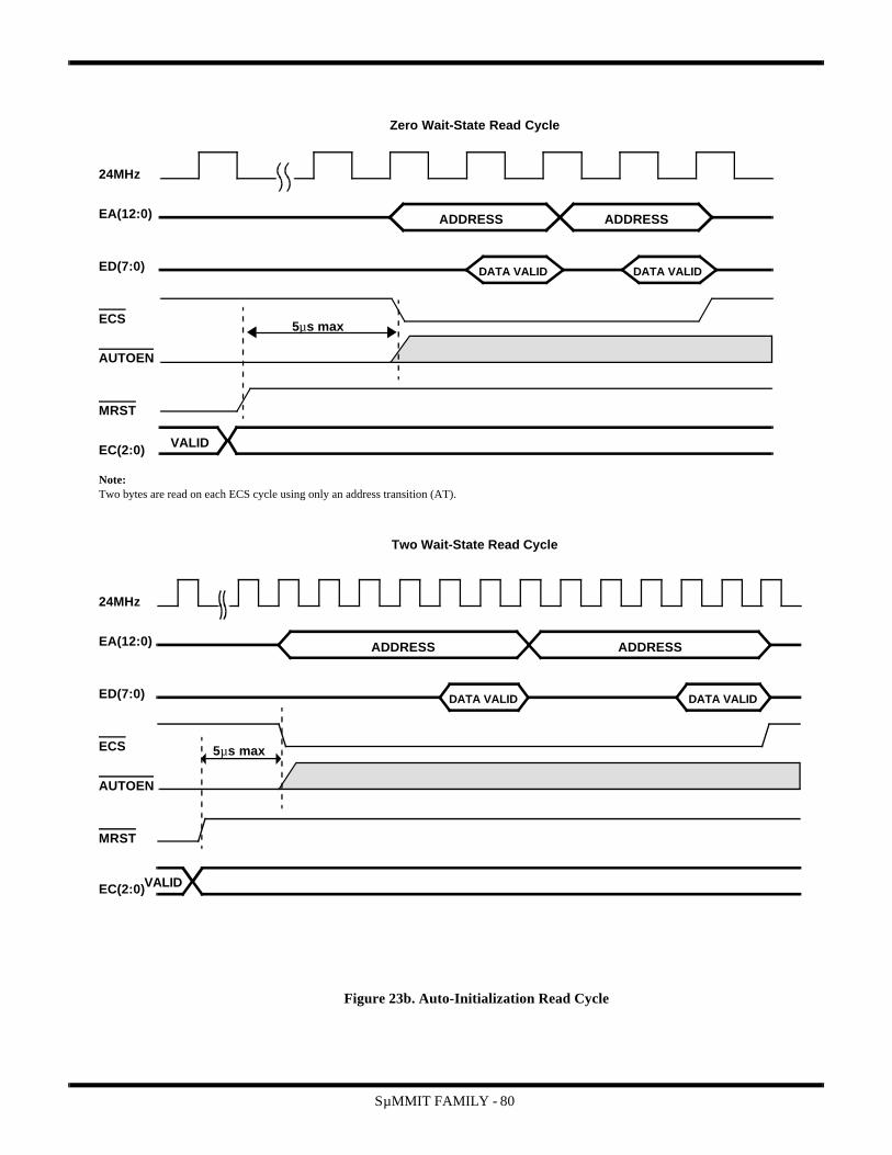
SµMMIT FAMILY - 80
Figure 23b. Auto-Initialization Read Cycle
24MHz
EA(12:0)
ED(7:0)
ECS
AUTOEN
MRST
5µs max
Zero Wait-State Read Cycle
ADDRESS
DATA VALID
24MHz
EA(12:0)
ED(7:0)
ECS
AUTOEN
MRST
Two Wait-State Read Cycle
ADDRESS
DATA VALID
EC(2:0)
EC(2:0)VALID
VALID
5µs max
Note:Two bytes are read on each ECS cycle using only an address transition (AT).
DATA VALID
ADDRESS
DATA VALID
ADDRESS

8.0 TestabilityThe following sections review the built-in test capabilities of the SMMIT family. The SMMIT family ranges from the simple SMMIT E to the complex SMMIT XTE. The varying complexity results in slightly different test techniques to exercise each product type. Table 13 is a list of the various components that comprehend each of the different SMMIT product.
A SMMIT product’s built-in test (BIT) varies depending on the product’s internal component mix and the BIT initiating sequence. BIT’s execution time will also vary depending on the number of internal components under test. Table 14 reviews the various BIT initiation sequences and the components that the sequence tests along with BIT execution times.
Notes:1. The transceiver is tested with the data wrap-around feature of the SMMIT family. See sections 2.1.5, 3.1.5, 4.1.5.2. Control Register write of 400016. Before initiating memory test, reset the SMMIT XTE by asserting MRST.
3. Remote Terminal mode of operation, BIT initiated after reception of mode code command.4. Bus Controller mode of operation, BIT initiated after the fetch of a command block containing an initiate BIT op-code.5. SMMIT test 1mS. Memory test 70mS.6. JTAG can operate up to 1MHz.
Table 2: Table 13. SMMIT Family Internal Component List
Product Protocol Die Transceivers Memory MMU
SMMIT E Yes No No No
SMMIT LXE Yes Yes No No
SMMIT DXE Yes Yes No No
SMMIT XTE Yes Yes Yes Yes
Table 3: Table 14. BIT Initiation
Initiation Type Protocol Die Transceivers1 Memory MMUExecution
Time2
CPU Initiated2 Yes No Yes No 1mS/80mS
Mode Code Initiated4 Yes No No No 1mS
Op-Code Initiated5 Yes No No No 1mS
JTAG 1149.16 Yes No No Yes N/A
JTAG/RUNBIST Yes No No No 1mS
SMMIT FAMILY - 81

SMMIT FAMILY - 82
9.0 SYSTEM CONFIGURATION
9.1 SMMIT E & SMMIT LXE/DXE
9.1.1 Transmitter/Receiver InterfaceThe SMMIT Manchester II encoder/decoder interfaces directly with the UT63M100 Series Bus Transceiver, using TA-TA and RA-RA signals for Channel A, and TB-TB and RB-RB signals for Channel B. See appendix 1 for additional information on UTMC transceivers. The SMMIT also provides TIMERONA and TIMERONB output signals to assist in meeting the MIL-STD-1553B fail-safe timer requirements (see figures 24a and 24b). Reference section 10 for SMMIT LXE/DXE serial bus interface information.
RXOUT
RXOUT
TXIN
TXIN
TXINHB
TXINHB
RXOUTRXOUT
UTMCUT63M100 SERIES
SMMIT
UT69151
RA
RA
RB
RB
TXIN
TXIN
TA
TA
TIMERON
TIMERO
TB
TB
Figure 24b. SMMIT Transceiver Interface Diagram
HOST SUBSYSTEM
ADDR(15:0)
DATA(15:0)
CONTROL
UT63M100 SERIES1553 TRANSCEIVER
1553 BUS A
SMMIT
UT69151
1553 BUS B
Figure 24a. SMMIT General System Diagram

SMMIT FAMILY - 83
9.1.2 Register TransfersThe host’s or subsystem’s access to the SMMIT E & SMMIT LXE/DXE internal registers is similar to its access to RAM. After gaining control of the memory bus, the host supplies address information to bidirectional address bus pins A(4:0). After supplying the address information, the host asserts SMMIT E & SMMIT LXE/DXE inputs CS and RD/WR to designate a register access and the type of access. The memory access terminates on the negation of CS. For more information on register cycles refer to the timing diagrams and AC electrical specifications in section 20. For register utilization versus mode of operation see Table 15.
Note: Modifying (i.e., writing) internal registers is not recommended while the SMMIT E & SMMIT LXE/DXE is processing messages (i.e., TERACT active). The only exception occurs when the SMMIT E & SMMIT LXE/DXE is in the SBC mode of operation where a write to bit 15 of the Control Register is permitted.
Table 15. Internal Register Utilization
Register Number
Register Number
8-Bit Mode(SMMIT XTE only)
RegisterName
SRT SBC SMT
0 0,1 Control
1 2,3 Operational Status
2 4,5 Current Command
3 6,7 Interrupt Mask
4 8,9 Pending Interrupt
5 A,B Interrupt Log List
6 C,D BIT Word
7 E,F Time Tag (SRT and SMT)Miner Frame Timer (SBC)
8 10,11 SRT Descriptor Pointer (SRT)Command Block Pointer (SBC)
9 12,13 1553 Status Word Bits
A 14,15 Command Block Initialization Count (BC)
B 16,17 Initial Monitor Command Block Pointer
C 18,19 Initial Monitor Data Pointer
D 1A,1B Monitor Block Count
E 1C,1D Monitor Filter
F 1E,1F Monitor Filter
10 to 1F 20 to 3F Illegalization (16)
Total 26 10 13

84 SMMIT FAMILY
9.1.3 DMA ConfigurationFor a DMA system configuration the SMMIT & SMMIT LX/DX shares memory with the host and/or subsystem. The SIT & SMMIT LX/DX gains access to memory through an arbitration process. The SIT & SMMIT LX/DX requests access to memory by asserting the DMAR signal. After receiving a grant signal (i.e., assertion of DMAG) from the bus arbiter, the SIT & SMMIT LX/DX asserts DMACK to acknowledge control of the bus. The SIT & SMMIT LX/DX continues to assert DMACK until all accesses are complete. After completion of all accesses, DMACK negates releasing the bus. Figure 25 shows an example DMA system configuration.
9.1.4 DMA Transfers Following the assertion of DMACK, the SMMIT activates the address bus A(15:0). During write cycles, the bidirectional data bus D(15:0) activates, supplying data for the write cycle. For read cycles, the bidirectional data bus remains an input. Memory control signals RCS, RRD, and RWR assert following the address bus activation. These signals control the memory chip select, output enable and write inputs. Table 16 is a summary of DMA activity during message processing.
For both read and write memory cycles, DTACK is an input to the SMMIT& SMMIT LX/DX. A non-wait state memory access requires two clock cycles. For accessing slower memory devices, hold DTACK to a logical one. This results in the stretching of memory cycles beyond the two clock cycles. The SMMIT & SMMIT LX/DX samples DTACK on the rising edge of the 24 MHz clock. If the memory logic fails to assert DTACK before the rising edge of the clock, the SMMIT & SMMIT LX/DX extends the memory cycle. One clock cycle is added to the memory cycle and DTACK is again sampled on the clock rising edge. If DTACK remains negated, the SMMIT & SMMIT LX/DX continues to add one clock cycle to the memory cycle and samples DTACK on each rising edge of the clock.
Aeroflex’s UT54ACTS220 automatically generates one wait state for either the SMMIT E or SMMIT LXE/DXE. See Figure 26 for additional information. Figure 26 shows a block diagram of the UT54ACTS220. See Aeroflex’s Logic Products website at www.aeroflex.com/Logic for additional information.
Assertion of DTACK signals the SMMIT & SMMIT LX/DX to terminate the memory cycle. The memory cycle terminates one clock cycle after DTACK assertion. For more information on memory cycles, refer to the timing diagrams and AC electrical specifications in section 20.
9.1.5 Buffer Mode OperationThe SMMIT & SMMIT LX/DX have the optional use of an internal 32-word buffer to enhance message processing. Use of this internal buffer decreases the number of times the SMMIT & SMMIT LX/DX arbitrates for memory during message processing. The number of memory accesses required to process a command is dependent on the mode of operation (SRT, SBC, SMT).
The SMMIT & SMMIT LX/DX stores all data words associated with a receive message into memory using a single DMA burst. When transmitting information, the SMMIT & SMMIT LX/DX arbitrates for a memory access and extracts all data for transmission from external memory in a single DMA burst. For either receive or transmit messages, the SMMIT & SMMIT LX/DX does not release the memory bus until all data is transferred to or from external memory. The buffer mode of operation eliminates the SMMIT & SMMIT LX/DX arbitration for the bus each time a data word memory access is required.
To enable use of the internal message buffer, the host asserts bit 6 of the Control Register. If the buffer feature is not enabled, the SMMIT & SMMIT LX/DX arbitrates each time data storage or retrieval is required. The host or subsystem does not have access to this internal buffer.

85SMMIT FAMILY
Figure 25. DMA System Configuration
CPU SMMIT
ARBITER
ARBITRATIONCONTROL SIGNALS
DMAMEMORY
ADDRESS BUS
DATA BUS
MEMORY CONTROL SIGNALS
ARBITRATIONCONTROL SIGNALS
RWR
UT54ACTS220
RRD
DTACK
DMACK
RCS
SMMIT or
SMMIT LX/DXMemory
24MHz
48MHzOscillator
Figure 26. Wait-State Configuration using UT54ACTS220

SMMIT FAMILY - 86
Table 16. DMA BC Write Scenario
BC Read Scenario
Monitor Write Scenario
RT Write Scenario
RT Read Scenario
Note: 1. If buffer mode selected, more than 1 and up to 32 words can be read/written.
Number of Words Word Type
1-321 Data Word
2 Interrupt Information Word Interrupt Address Word
6 Control WordCmd Word 1Cmd Word 2Data PointerStatus Word 1Status Word 2
8 Control WordCmd Word 1Cmd Word 2Data PointerStatus Word 1Status Word 2Interrupt Information WordInterrupt Address Word
Number of Words Word Type
1-321 Data Word
8 Control WordCmd Word 1Cmd Word 2Data PointerStatus Word 1Status Word 2Branch AddressTimer Value
Number of Words Word Type
1-321 Data Word
7 Control WordCmd Word 1Cmd Word 2Data PointerStatus Word 1Status Word 2Time Tag
9 Control WordCmd Word 1Cmd Word 2Data PointerStatus Word 1Status Word 2Time TagInterrupt Status WordInterrupt Address Word
Number of Words Word Type
1-321 Data Word
3 Message Information WordTime-Tag WordControl Word
4 Message Information WordTime-Tag WordControl WordData Pointer
5 Message Information WordTime-Tag WordControl WordInterrupt Information WordInterrupt Address Word
6 Message Information WordTime-Tag WordControl WordData PointerInterrupt Information WordInterrupt Address Word
Number of Words Word Type
1-321 Data Word
4 Control WordData Pointer AData Pointer BBroadcast Data Pointer

SµMMIT FAMILY - 87
9.2 SµMMIT XTEThe SµMMIT XTE supplies hardware designers with a flexible interface to meet the needs of state-of-the-art MIL-STD-1553 interfaces. The SµMMIT XTE contains internal SRAM and a memory management unit, interfaces to either 8-bit or 16-bit subsystems, supports multiplexed and non-multiplexed interfaces, and has user selectable control signals.
9.2.1 Internal Registers The SµMMIT XTE contains 32 internal registers that control and report on message activity and operation. The 32 registers are memory mapped into the subsystem memory. Table 17 reviews the registers and identifies the mode of operation applicable. The host reads or writes these registers using the timing diagrams shown in figures 27 a-d.
9.2.2 Memory MapThe SµMMIT XTE contains 512Kbits of memory for message storage and system data storage. MSEL(5) determines the organization of the memory as either by 16 or by 8. When organized by 16 (i.e., MSEL(5) = 0) the SµMMIT XTE’ s internal memory looks like 32K x 16 of SRAM. For by 8
applications (MSEL(5) = 1) the SµMMIT XTE’s internal memory looks like 64K x 8 of SRAM. The host reads or writes SRAM using the timing diagrams shown in figures 27 a-d. Table 17 shows the memory organization for either 8-bit or 16-bit operation.
9.2.3 Buffer Mode OperationFor the SµMMIT XTE operation, disable buffer mode, i.e, control register bit 6 = Logic 0.
9.2.4 Hardware InterfaceThe SµMMIT XTE offers hardware designers a flexible interface to commonly found embedded computers. The hardware designer selects control signals, bus widths, and bus functionality (i.e., non-multiplexed versus multiplexed) to meet their interface requirements. Table 18 reviews how the user selects the SµMMIT XTE’s operation that best meets their interface requirements.
Figures 28 a-d show typical system interfaces and use of the mode select inputs to configure the SµMMIT XTE to interface to various embedded computers.
Table 17. Memory Organization
Table 18. User-Selectable Control Signals
Mode Memory Organization Register Location Memory Range
8-bit 64K x 8 0000 (hex) to 003F (hex) 0040 (hex) to FFFF (hex)
16-bit 32K x 16 0000 (hex) to 001F (hex) 0020 (hex) to 7FFF (hex)
Function Input Pin Logic 1 Logic 0
Control Signal Select MSEL(2) R/WR, CS, DS, RDY RD, WR, CS, RDY, DS
Bus Functionality Select MSEL(3) Non-Multiplexed Address and Data
Multiplexed Address and Data, ALE
Interrupt Select MSEL(4) Level (YF_INT, MSG_INT, YF_ACK, and MSG_ACK)
Pulse (YF_INT and MSG_INT)
Bus Width Select MSEL(5) 8-bit 16-bit

SµMMIT FAMILY - 88
Figure 27a. 8-bit Memory and Register Access
A(15:0)
Non-Multiplexed Memory/Register Read Access (8-bit Mode)1,2
ADDRESS ADDRESS
CS
Notes:1. ALE must be tied high.2. Latter assertion of CS, DS, RD starts cycle.3. Tie DA(15:8) to VDD via a 10K resistor.4. When using R/WR as an input signal tie RD to a logical one. During the read cycle R/WR remains a logical 1.5. DS asserts to signal the SµMMIT XTE to place data on the bus.
RD4
DA(7:0) 3BYTE BYTE
RDY
DS 5
A(15:0)
Non-Multiplexed Memory Register Write Access (8-bit Mode)1, 2
WR or R/WR
CS
RDY
DA(7:0) 3
ADDRESS VALID
LOW BYTE HIGH BYTE
DS 4
Notes:1. ALE must be tied high.2. Latter assertion of CS, DS, WR or R/WR starts cycle.3. Tie DA(15:8) to VDD via a 10K resistor.4. DS asserts to signal that data is valid on the bus.

SµMMIT FAMILY - 89
Figure 27b. 16-bit Memory and Register Access
A(14:0)3
Non-Multiplexed Memory/Register Write Access (16-bit Mode)1, 2
A(14:0)3
Non-Multiplexed Memory/Register Read Access (16-bit Mode)1,2
ADDRESS
CS
Notes:1. ALE must be tied high.2. Latter assertion of CS, DS, RD starts cycle.3. A15 must be tied low.4. When using R/WR as an input signal tie RD to a logical one. During the read cycle R/WR remains a logic 1.5. DS asserts to signal the SµMMIT XTE to place data on the bus.
Notes:1. ALE must be tied high.2. Latter assertion of CS, DS, WR or R/WR starts cycle.3. A15 must be tied low.4. DS asserts to signal that data is valid on the bus.
WR or R/WR
RD 4
CS
RDY
DA(15:0)
DA(15:0)
ADDRESS
VALID WORD
VALID WORD
RDY
DS 4
DS 5

SµMMIT FAMILY - 90
Figure 27c. Multiplexed 8-bit Memory and Register Access
DA(15:0) 2,3
Multiplexed Memory/Register Read Access (8-bit Mode)1
CS
RD4
ALE
BYTE BYTEADDRESS ADDRESS
RDY
DS 5
DA(15:0) 2,3
Multiplexed Memory Register Write Access (8-bit Mode)1
Notes:
1. Latter assertion of CS, DS, WR or R/WR starts cycle.2. For multiplexed address and data interfaces ALE latches the address into the SµMMIT XTE. Data is applied to inputs DA(7:0), tie A(15:0) to either a logical one or zero.3. Tie DA(15:8) to VSS via a 10K resistor.4. DS asserts to signal that data is valid on the bus.
WR or R/WR
ALE
CS
RDY
LOW BYTE HIGH BYTEADDRESS ADDRESS
DS 4
Notes:1. Latter assertion of CS, DS, RD starts cycle.2. For multiplexed address and data interfaces ALE latches the address into the SµMMIT XTE.
Data is read from outputs DA(7:0), tie A(15:0) to either a logical one or zero.3. Tie DA(15:8) to VSS via a 10K resistor.4. W hen using R/WR as an input signal tie RD to a logical one. During the read cycle R/WR remains a logic 1.5. DS asserts to signal the SµMMIT XTE to place data on the bus.

SµMMIT FAMILY - 91
Figure 27d. Multiplexed 16-bit Memory and Register Access
DA(15:0) 2
Multiplexed Memory/Register Write Access (16-bit Mode)1
DA(15:0) 2
Multiplexed Memory/Register Read Access (16-bit Mode)1
CS
Notes:
1. Latter assertion of CS, DS, RD starts cycle.2. For multiplexed address and data interfaces ALE latches the address into the SµMMIT XTE.
Data is read from outputs DA(15:0), tie A(15:0) to either a logical one or zero.3. DS asserts to signal the SµMMIT XTE to place data on the bus.
Notes:1. Latter assertion of CS, DS, WR or R/WR starts cycle.2. For multiplexed address and data interfaces ALE latches the address into the SµMMIT XTE.
Data is applied to inputs DA(15:0), tie A(15:0) to either a logical one or zero.3. DS asserts to signal that data is valid on the bus.
WR or R/WR
RD
ALE
ALE
CS
DS3
DS 3
DATAADDRESS
DATAADDRESS
RDY
RDY

SµMMIT FAMILY - 92
Figure 28a. 16-bit Interface (Intel Type)
Figure 28b. 16-bit Interface (Motorola Type)
SµMMIT XTE TRANSFORMERCHANNEL A
TRANSFORMERCHANNEL B
CHA
CHA
CHB
CHB
DA(15:0)
ALE
RD
WR
MSEL(5)
MSEL(2)
MSEL(3)
TYPE CPUTRANSFORMER
CHANNEL A
TRANSFORMERCHANNEL B
CHA
CHA
CHB
CHB
A(15:0)
R/WR
CS
CS
DA(7:0)TO 1553BUS A
TO 1553BUS B
TO 1553BUS A
TO 1553BUS B
SµMMIT XTE
INTEL TYPECPU
MOTOROLA
DS
READY RDY
MSEL(2)
MSEL(3)
MSEL(5)

SµMMIT FAMILY - 93
Figure 28c. 8-bit Interface (Intel Type)
Figure 28d. 8-bit Interface (Motorola Type)
SµMMIT XTE TRANSFORMERCHANNEL A
TRANSFORMERCHANNEL B
CHA
CHA
CHB
CHB
DA(15:0)
ALE
RD
WR
MSEL(5)
MSEL(2)
MSEL(3)
TYPE CPUTRANSFORMER
CHANNEL A
TRANSFORMERCHANNEL B
CHA
CHA
CHB
CHB
A(15:0)
R/WR
CS
MSEL(5)
MSEL(3)
MSEL(2)
CS
DA(7:0)TO 1553BUS A
TO 1553BUS B
TO 1553BUS A
TO 1553BUS B
SµMMIT XTE
INTEL TYPECPU
MOTOROLA
DS

SµMMIT FAMILY - 94
10.0 SERIAL DATA BUS INTERFACE
The SµMMIT LXE/DXE & SµMMIT XTE Manchester encoder/decoder interfaces directly to the MIL-STD-1553 bus via transformers, using CHA-CHA and CHB-CHB. The designer can connect the SµMMIT LXE/DXE & SµMMIT XTE to the data bus via a short-stub (direct-coupling) connection or a long-stub (transformer-coupling) connection. Use a short-stub connection when the distance from the isolation transformer to the data bus does not exceed a one-foot maximum. Use a long-stub connection when the distance from the isolation transformer exceeds the one-foot maximum and is less than twenty feet. Figures 29 a-c show various examples of bus coupling configurations. The SµMMIT LXE/DXE & SµMMIT XTE is designed to function with MIL-STD-1553A and 1553B compatible transformers.
10.1 TransmitterThe transmitter section accepts Manchester II biphase TTL data and converts this data into differential phase-modulated current drive. Transmitter current drivers are coupled to a MIL-STD-
1553 data bus via a transformer driven from the CHA (CHB) and CHA (CHB) terminals. The SµMMIT LXE/DXE & SµMMIT XTE internally generates a signal to the transceiver for the MIL-STD-1553 fail-safe timer requirement.
10.2 ReceiverThe receiver section accepts biphase differential data from a MIL-STD-1553 data bus at its CHA (CHB) and CHA (CHB) inputs. The receiver converts input data to biphase Manchester II TTL format at internal RXOUT and RXOUT terminals. The internal outputs RXOUT and RXOUT represent positive and negative excursions (respectively) of the inputs CHA (CHB) and CHA (CHB).
10.3 Recommended Thermal ProtectionAll packages should mount to or contact a heat removal rail located in the printed circuit board. To insure proper heat transfer between the package and the heat removal rail, use a thermally-conductive material between the package and the heat removal rail. Use a material such as Mereco XLN-589 or equivalent to insure heat transfer between the package and heat removal rail.
OPERATION
55 OHMS
55 OHMS
1 FT MAX
20 FT MAX
SHORT-STUBDIRECT COUPLING
LONG-STUBTRANSFORMER COUPLING
1.4:1
2:1 1:1.4
-15VDC
ZO
.75 ZO
.75 ZO
ZONote:ZO defined per MIL-STD-1553B in section 4.5.1.5.2.1.
Figure 29a. SµMMIT LXE15, XTE15 Bus Coupling Configuration
CHA
CHA
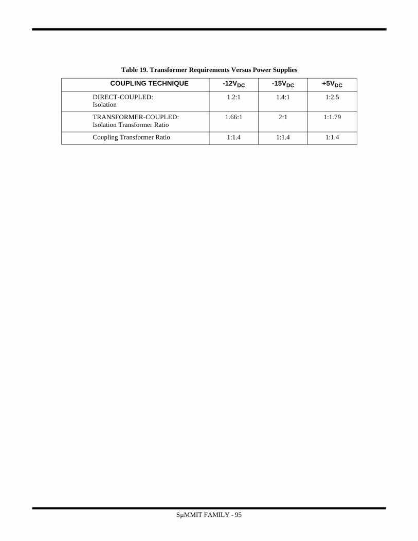
SµMMIT FAMILY - 95
Table 19. Transformer Requirements Versus Power Supplies
COUPLING TECHNIQUE -12VDC -15VDC +5VDC
DIRECT-COUPLED:Isolation
1.2:1 1.4:1 1:2.5
TRANSFORMER-COUPLED:Isolation Transformer Ratio
1.66:1 2:1 1:1.79
Coupling Transformer Ratio 1:1.4 1:1.4 1:1.4

SµMMIT FAMILY - 96
20 FT MAX
OPERATION
55 OHMS
55 OHMS
1 FT MAX
SHORT-STUBDIRECT COUPLING
LONG-STUBTRANSFORMER COUPLING
1:1.4
1.2:1
1.66:1
Note:ZO defined per MIL-STD-1553B in section 4.5.1.5.2.1.
-12VDC
.75 ZO
.75 ZO
ZO
ZO
Figure 29b. SµMMIT LXE12, XTE12 Bus Coupling Configuration
55 OHMS
55 OHMS
20 FT MAX 1:1.4
ZO
ZO
+5V DC
OPERATION
1:1.79
1:2.5
SHORT-STUBDIRECT COUPLING
1 FT. MAX.
LONG-STUBTRANSFORMER COUPLING
.75 ZO
.75 ZO
CHA
CHA
Figure 29c. SµMMIT DXE, XTE5 Bus Coupling Configuration
Note:ZO defined per MIL-STD-1553B in section 4.5.1.5.2.1.
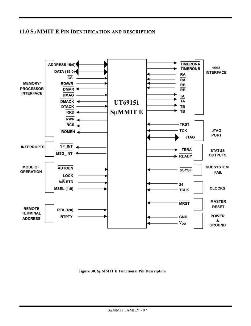
11.0 SMMIT E PIN IDENTIFICATION AND DESCRIPTION
UT69151
SMMIT E
Figure 30. SMMIT E Functional Pin Description
MEMORY/
PROCESSORINTERFACE
JTAGPORT
STATUSOUTPUTS
CLOCKS
POWER&
GROUND
MODE OFOPERATION
REMOTETERMINAL
ADDRESS
1553INTERFACE
SUBSYSTEM
FAIL
MASTER
RESET
INTERRUPTS
TIMERONATIMERONB
RA
RARBRB
TATA
TBTB
CS
DMAR
DMAG
DMACKDTACK
RRD
RWR
RCS
ROMEN
RD/WR
DATA (15:0)
AUTOEN
LOCK
RTA (4:0)
RTPTY
A/B STD
MSEL (1:0)
YF_INT
MSG_INTTERA
MRST
SSYSF
READY
TRST
24
TCLK
VDD
GND
TCK
JTAG
ADDRESS 15:0)
SMMIT FAMILY - 97

11.1 SMIT E Functional Pin Description
Legend for TYPE and ACTIVE fields1:TO = TTL outputTTB = Three-state TTL bidirectionalCI = CMOS inputTUI = TTL input (internally pulled high)AH = Active highAL = Active lowTI = TTL input OD = Open DrainTTO = Three-state TTL output PGA = Pingrid ArrayFP = Flatpack[ ] = 132-lead FlatpackNote:1. All pins described as TTL use CMOS transistors that are designedcompatibility with TTL devices.
11.1.1 Data Bus
Bit Number
Type Active Pin Number FP PGA
Description
15 TTB -- 4 [7] C1 Bit 15 (MSB) of the bidirectional Data bus.
14 TTB -- 5 [8] D2 Bit 14 of the bidirectional Data bus.
13 TTB -- 6 [9] D1 Bit 13 of the bidirectional Data bus.
12 TTB -- 7 [10] F2 Bit 12 of the bidirectional Data bus.
11 TTB -- 8 [11] E2 Bit 11 of the bidirectional Data bus.
10 TTB -- 9 [15] E1 Bit 10 of the bidirectional Data bus.
9 TTB -- 10 [18] F1 Bit 9 of the bidirectional Data bus.
8 TTB -- 13 [19] G1 Bit 8 of the bidirectional Data bus.
7 TTB -- 14 [20] G2 Bit 7 of the bidirectional Data bus.
6 TTB -- 15 [24] G3 Bit 6 of the bidirectional Data bus.
5 TTB -- 16 [25] H1 Bit 5 of the bidirectional Data bus.
4 TTB -- 17 [26] H2 Bit 4 of the bidirectional Data bus.
3 TTB -- 18 [27] J1 Bit 3 of the bidirectional Data bus.
2 TTB -- 19 [30] K1 Bit 2 of the bidirectional Data bus.
1 TTB -- 20 [31] J2 Bit 1 of the bidirectional Data bus.
0 TTB -- 21 [32] L1 Bit 0 (LSB) of the bidirectional Data bus.
SMMIT FAMILY - 98
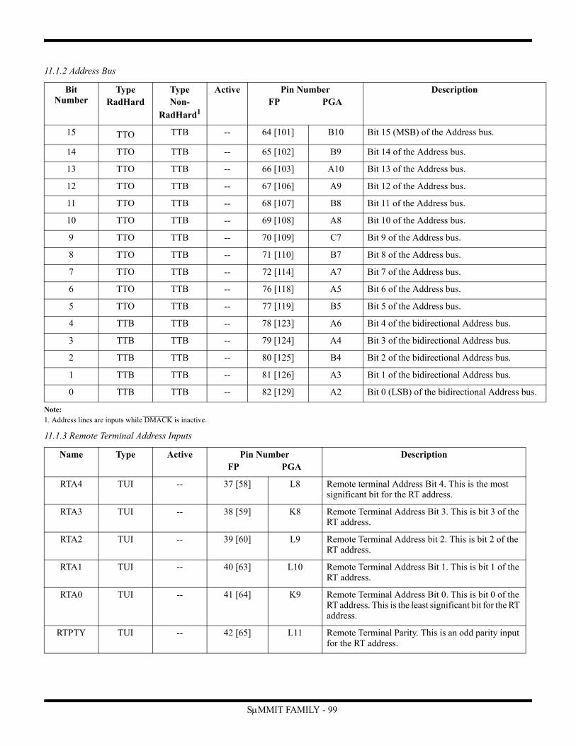
11.1.2 Address Bus
Note:1. Address lines are inputs while DMACK is inactive.
11.1.3 Remote Terminal Address Inputs
Bit Number
TypeRadHard
TypeNon-
RadHard1
Active Pin Number FP PGA
Description
15 TTO TTB -- 64 [101] B10 Bit 15 (MSB) of the Address bus.
14 TTO TTB -- 65 [102] B9 Bit 14 of the Address bus.
13 TTO TTB -- 66 [103] A10 Bit 13 of the Address bus.
12 TTO TTB -- 67 [106] A9 Bit 12 of the Address bus.
11 TTO TTB -- 68 [107] B8 Bit 11 of the Address bus.
10 TTO TTB -- 69 [108] A8 Bit 10 of the Address bus.
9 TTO TTB -- 70 [109] C7 Bit 9 of the Address bus.
8 TTO TTB -- 71 [110] B7 Bit 8 of the Address bus.
7 TTO TTB -- 72 [114] A7 Bit 7 of the Address bus.
6 TTO TTB -- 76 [118] A5 Bit 6 of the Address bus.
5 TTO TTB -- 77 [119] B5 Bit 5 of the Address bus.
4 TTB TTB -- 78 [123] A6 Bit 4 of the bidirectional Address bus.
3 TTB TTB -- 79 [124] A4 Bit 3 of the bidirectional Address bus.
2 TTB TTB -- 80 [125] B4 Bit 2 of the bidirectional Address bus.
1 TTB TTB -- 81 [126] A3 Bit 1 of the bidirectional Address bus.
0 TTB TTB -- 82 [129] A2 Bit 0 (LSB) of the bidirectional Address bus.
Name Type Active Pin Number FP PGA
Description
RTA4 TUI -- 37 [58] L8 Remote terminal Address Bit 4. This is the most significant bit for the RT address.
RTA3 TUI -- 38 [59] K8 Remote Terminal Address Bit 3. This is bit 3 of the RT address.
RTA2 TUI -- 39 [60] L9 Remote Terminal Address bit 2. This is bit 2 of the RT address.
RTA1 TUI -- 40 [63] L10 Remote Terminal Address Bit 1. This is bit 1 of the RT address.
RTA0 TUI -- 41 [64] K9 Remote Terminal Address Bit 0. This is bit 0 of the RT address. This is the least significant bit for the RT address.
RTPTY TUI -- 42 [65] L11 Remote Terminal Parity. This is an odd parity input for the RT address.
SMMIT FAMILY - 99

11.1.4 JTAG Testability Pins
11.1.5 Biphase Inputs
Name Type Active Pin Number FP PGA
Description
TDO TTO -- 49 [79] G9 TDO. This output performs the operation of Test Data Output as defined in the IEEE Standard 1149.1. This non-inverting output buffer is optimized for driving TTL loads.
TCK TUI -- 54 [84] E9 TCK. This input performs the operation of Test Clock input as defined in the IEEE Standard 1149.1. This non-inverting input buffer is optimized for driving TTL input levels. Can operate up to 1MHz.
TMS TUI -- 51 [81] G11 TMS. This input performs the operation of Test Mode Select as defined in the IEEE Standard 1149.1. This non-inverting input buffer is optimized for driving TTL input levels.
TDI TUI -- 50 [80] G10 TDI. This input performs the operation of Test Data In as defined in the IEEE Standard 1149.1. This non-inverting input buffer is optimized for driving TTL input levels.
TRST TUI AL 48 [78] H11 TRST. This input provides the RESET to the TAP controller as defined in the IEEE Standard 1149.1. This non-inverting input buffer is optimized for driving TTL input levels. When not exercising JTAG, tie TRST to a logical 0.
Name Type Active Pin Number FP PGA
Description
RA TI -- 26 [41] K4 Receive Channel A (True). This is the Manchester-encoded true signal input for channel A. (Quiescent low).
RA TI -- 25 [38] L3 Receive Channel A (Complement). This is the Manchester-encoded complement signal input for channel A. (Quiescent low).
RB TI -- 33 [51] J5 Receive Channel B (True). This is the Manchester-encoded true signal input for channel B. (Quiescent low).
RB TI -- 30 [48] L5 Receive Channel B (Complement). This is the Manchester-encoded complement signal input for channel B. (Quiescent low).
SMMIT FAMILY - 100

11.1.6 Biphase Outputs
Note:1. These pins are driven low while MRST is low and 24MHz is active.
11.1.7 DMA Signals
Note:1. This output will drive low and three-state only.
Name Type Active Pin Number FP PGA
Description
TA TO1 -- 24 [37] L2 Transmit Channel A (True). This is the Manchester-encoded true signal output for channel A. The signal is idle low. (Quiescent low).
TA TO1 -- 23 [36] K3 Transmit Channel A (Complement). This is the Manchester-encoded complement signal output for channel A. The signal is idle low. (Quiescent low).
TB TO1 -- 29 [44] K5 Transmit Channel B (True). This is the Manchester-encoded true signal output for channel B. The signal is idle low. (Quiescent low).
TB TO1 -- 28 [43] K6 Transmit Channel B (Complement). This is the Manchester-encoded complement signal output for channel B. The signal is idle low. (Quiescent low).
Name Type Active Pin Number FP PGA
Description
DMAR OD1 AL 55 [85] E11 DMA Request. This signal is asserted when access to RAM is required. It goes inactive upon receipt of the DMAG signal.
DMAG TI AL 56 [86] E10 DMA Grant. Once this input is received, the SIT is allowed to access RAM.
DMACK OD1 AL 57 [90] F11 DMA Acknowledge. This signal is asserted by the SIT to indicate the receipt of DMAG. The signal remains active until all RAM bus activity is completed.
DTACK TI AL 3 [4] B1 Data Transfer Acknowledge. This pin indicates that a data transfer is to occur and that the SIT may complete the memory cycle.
SMMIT FAMILY - 101

11.1.8 Control Signals
Note:1. This output will drive low and three-state only.
Name Type Active Pin Number FP PGA
Description
RD/WR TI -- 63 [98] A11 Read/Write. This indicates the direction of data flow with respect to the host. A logic high signal means the host is trying to read data from the SIT, and a logic low signal means the host is trying to write data to the SIT.
CS TI AL 62 [97] C10 Chip Select. This pin selects the SIT when accessing the internal registers.
RRD TTO AL 84 [131] A1 RAM Read. This signal is generated by the SIT to read data from RAM.
RWR TTO AL 83 [130] B3 RAM Write. This signal is generated by the SIT to write data to RAM.
RCS TTO AL 1 [2] B2 RAM Chip Select. This signal is used in conjunction with the RRD/RWR signals to access RAM.
AUTOEN TUI AL 60 [93] C11 Auto Enable. This pin, when active, enables automatic initialization.
ROMEN OD1 AL 61 [96] B11 ROM Enable. This pin, when active, enables the ROM for automatic initialization applications.
SSYSF TUI AL 36 [57] J7 Subsystem Fail. Upon receipt, this signal propagates directly to the RT 1553 Status Word.
24 MHz CI -- 75 [117] C5 24 MHz Clock. The 24MHz input clock requires a 50% +5% duty cycle with an accuracy of +0.01%. See Appendix A on UT54ACTS220 Clock Generator.
MRST TUI AL 47 [75] H10 Master Reset. This input pin resets the internal encoders, decoders, all registers, and associated logic.
MSEL(1) TI -- 45 [73] K11 Mode Select 1. This pin is the most significant bit for the mode select. For proper mode selection, see below: MSEL(1) MSEL(0) Mode of Operation 0 0 Bus Controller = SBC
0 1 Remote Terminal = SRT 1 0 Monitor Terminal =SMT 1 1 SMT/SRT
MSEL(0) TI -- 46 [74] J11 Mode Select 0. This pin is the least significant bit for the mode select. (See MSEL1 for proper logic states.)
SMMIT FAMILY - 102

11.1.8 Control Signals (continued)
Note:1. High impedance and active low.
11.1.9 Status Signals
Note:1. This output will drive low and three-state only.2. These pins are driven high while MRST is low and 24MHz is active.
Name Type Active Pin Number FP PGA
Description
TCLK TI -- 2 [3] C2 Timer Clock. The internal timer is a 16-bit counter with a 64s resolution when using the 24MHz input clock. For different applications, the user may input a clock (0-6MHz) to establish the timer resolution. (Duty Cycle = 50% +10%).
A/B STD TUI -- 44 [69] J10 Military Standard A or B. This pin defines whether the SIT will be used in a MIL-STD-1553A or 1553B mode of operation.
LOCK TUI AL 43 [68] K10 Lock. This pin, when set active, prevents software changes to both the RT address, A/B STD, and mode select.
Name Type Active Pin Number FP PGA
Description
TERACT TO2 AL 34 [52] L7 Terminal Active. This output pin indicates that the terminal is actively processing a 1553 command.
TIMERONA
TO2 AL 22 [35] K2 Timer On A. This is a 800s fail-safe transmitter enable timer for channel A. This output is reset on receipt of a new command or after 760s.
TIMERONB
TO2 AL 27 [42] L4 Timer On B. This is a 800s fail-safe transmitter enable timer for channel B. This output is reset on receipt of a new command or after 760ms.
MSG_INT OD1 AL 58 [91] D11 Message Interrupt. This pin is active for three clock cycles (i.e., 125ns pulse) upon the occurrence of interrupt events which are enabled.
YF_INT OD1 AL 59 [92] D10 You Failed Interrupt. This pin is active for three clock cycles (i.e., 125ns pulse) upon the occurrence of interrupt events which are enabled.
READY TO2 AL 35 [53] K7 Ready. This signal indicates the SIT has completed a reset, an auto-initialization, or a BIT. After assertion of the READY signal initialization of the SIT for operation can begin.
SMMIT FAMILY - 103

11.1.10 Power/GroundThe following shows the package location of all power and ground pins associated with the SIT.
11.1.11 No Connects
Pin Number Pin Number FP PGA
Description
VDD 12, 32, 53, 73[17], [34], [50], [66],
[83], [100], [115], [132]
E3, L6, F9, C6 +5 Volt Power (+10%)
VSS 11, 31, 52, 74[1], [16], [33], [49],
[67], [82], [99], [116]
F3, J6, F10, B6 Digital Ground
Pin Number Pin Number FP PGA
Description
NC [5], [6], [12] [13], [14], [21], [22], [23], [28], [29], [39], [40], [45], [46], [47], [54], [55], [56], [61], [62], [70], [71], [72], [76], [77], [87], [88], [89], [94], [95], [104], [105], [111], [112], [113], [120],
[121], [122], [127], [128]
NA No Connects
SMMIT FAMILY - 104

12.0 SMMIT LXE/DXE PIN IDENTIFICATION AND DESCRIPTION
TERAC
AUTOEN
LOCK
CS
DMAR
DMAG
DMACKDTACK
RRD
RWR
RCS
ROMEN
MRST
SSYSF
READY
RTA (4:0)
RTPTY
RD/WR
A/B STD
MSEL (1:0)
TRS
DATA (15:0)
24
TCLK
VSS
VDD
UT69151 LXE/DXE
Figure 31. SMMIT LXE/DXE Functional Pin Description
VEE (LX
GND
MEMORY/
PROCESSORINTERFACE
JTAGPORT
STATUSOUTPUTS
CLOCKS
POWER&
GROUND
MODE OFOPERATION
REMOTETERMINAL
ADDRESS
CHA
CHB
CHA
CHB
1553INTERFACE
TCK
JTAG (2:0)
SUBSYSTEM
FAIL
MASTER
RESET
YF_INT
MSG_INT
INTERRUPTS
ADDRESS (15:0)
SMMIT FAMILY - 105

12.1 SMMIT LXE/DXE Pin Functional Description
Legend for TYPE and ACTIVE fields1:TO = TTL outputTTB = Three-state TTL bidirectionalCI = CMOS inputTUI = TTL input (internally pulled high)AH = Active highAL = Active lowTI = TTL input OD = Open drainTTO = Three-state TTL outputPGA = Pingrid ArrayFP = FlatpackDIO = Differential input/outputNote:1. All pins described as TTL use CMOS transistors that are designed compatibility with TTL devices.
12.1.1 Data Bus
Bit Number
Type Active Pin Number FP PGA
Description
15 TTB -- 97 V11 Bit 15 (MSB) of the bidirectional Data bus.
14 TTB -- 96 V5 Bit 14 of the bidirectional Data bus.
13 TTB -- 95 V9 Bit 13 of the bidirectional Data bus.
12 TTB -- 94 U10 Bit 12 of the bidirectional Data bus.
11 TTB -- 93 U12 Bit 11 of the bidirectional Data bus.
10 TTB -- 92 V15 Bit 10 of the bidirectional Data bus.
9 TTB -- 91 V13 Bit 9 of the bidirectional Data bus.
8 TTB -- 90 V17 Bit 8 of the bidirectional Data bus.
7 TTB -- 89 W18 Bit 7 of the bidirectional Data bus.
6 TTB -- 88 W16 Bit 6 of the bidirectional Data bus.
5 TTB -- 87 W14 Bit 5 of the bidirectional Data bus.
4 TTB -- 86 W20 Bit 4 of the bidirectional Data bus.
3 TTB -- 85 W22 Bit 3 of the bidirectional Data bus.
2 TTB -- 84 V21 Bit 2 of the bidirectional Data bus.
1 TTB -- 83 V19 Bit 1 of the bidirectional Data bus.
0 TTB -- 82 V23 Bit 0 (LSB) of the bidirectional Data bus.
SMMIT FAMILY - 106

12.1.2 Address Bus
Note:1. Address lines are inputs while DMACK is inactive.
12.1.3 Remote Terminal Address Inputs
Bit Number
TypeRadHard
TypeNon-
RadHard1
Active Pin Number FP PGA
Description
15 TTO TTB -- 26 A2 Bit 15 (MSB) of the Address bus.
14 TTO TTB -- 25 A4 Bit 14 of the Address bus.
13 TTO TTB -- 24 A6 Bit 13 of the Address bus.
12 TTO TTB -- 23 C2 Bit 12 of the Address bus.
11 TTO TTB -- 22 B3 Bit 11 of the Address bus.
10 TTO TTB -- 21 B5 Bit 10 of the Address bus.
9 TTO TTB -- 20 D1 Bit 9 of the Address bus.
8 TTO TTB -- 19 C6 Bit 8 of the Address bus.
7 TTO TTB -- 18 D3 Bit 7 of the Address bus.
6 TTO TTB -- 17 T7 Bit 6 of the Address bus.
5 TTO TTB -- 16 W2 Bit 5 of the Address bus.
4 TTB TTB -- 15 T3 Bit 4 of the bidirectional Address bus.
3 TTB TTB -- 14 T1 Bit 3 of the bidirectional Address bus.
2 TTB TTB -- 13 U6 Bit 2 of the bidirectional Address bus.
1 TTB TTB -- 12 U2 Bit 1 of the bidirectional Address bus.
0 TTB TTB -- 11 W6 Bit 0 (LSB) of the bidirectional Address bus.
Name Type Active Pin Number FP PGA
Description
RTA4 TUI -- 59 B17 Remote terminal Address Bit 4. This is the most significant bit for the RT address.
RTA3 TUI -- 58 B19 Remote Terminal Address Bit 3. This is bit 3 of the RT address.
RTA2 TUI -- 57 A20 Remote Terminal Address bit 2. This is bit 2 of the RT address.
RTA1 TUI -- 56 B21 Remote Terminal Address Bit 1. This is bit 1 of the RT address.
RTA0 TUI -- 55 A22 Remote Terminal Address Bit 0. This is bit 0 of the RT address. This is the least significant bit for the RT address.
RTPTY TUI -- 54 B23 Remote Terminal Parity. This is an odd parity input for the RT address.
SMMIT FAMILY - 107

12.1.4 JTAG Testability Pins
12.1.5 Biphase Inputs/Outputs
Name Type Active Pin Number FP PGA
Description
TDO TTO -- 52 A18 TDO. This output performs the operation of Test Data Output as defined in the IEEE Standard 1149.1. This non-inverting output buffer is optimized for driving TTL loads.
TCK TI -- 49 A14 TCK. This input performs the operation of Test Clock input as defined in the IEEE Standard 1149.1. This non-inverting input buffer is optimized for driving TTL input levels. Can operate up to 1MHz.
TMS TUI -- 50 C14 TMS. This input performs the operation of Test Mode Select as defined in the IEEE Standard 1149.1.This non-inverting input buffer is optimized for driving TTL input levels.
TDI TUI -- 51 A16 TDI. This input performs the operation of Test Data In as defined in the IEEE Standard 1149.1. This non-inverting input buffer is optimized for driving TTL input levels.
TRST TUI AL 53 B15 TRST. This input provides the RESET to the TAP controller as defined in the IEEE Standard 1149.1. This non-inverting input buffer is optimized for driving TTL input levels.When not exercising JTAG, tie TRST to a logical 0.
Name Type Active Pin Number FP PGA
Description
CHA DIO -- 32 U22 Channel A (True). This is the Manchester-encoded true signal for channel A.
CHA DIO -- 33 U18 Channel A (Complement). This is the Manchester-encoded complement signal input for channel A.
CHB DIO -- 42 C22 Channel B (True). This is the Manchester-encoded true signal for channel B.
CHB DIO -- 43 C18 Channel B (Complement). This is the Manchester-encoded complement signal for channel B.
SMMIT FAMILY - 108

12.1.6 DMA Signals
Note:1. This output will drive low and three-state only.
Name Type Active Pin Number FP PGA
Description
DMAR OD1 AL 3 D13 DMA Request. This signal is asserted when access to RAM is required. It goes inactive upon receipt of the DMAG signal.
DMAG TI AL 2 C10 DMA Grant. Once this input is received, the SIT LX/DX is allowed to access RAM.
DMACK OD1 AL 1 B7 DMA Acknowledge. This signal is asserted by the SIT LX/DX to indicate the receipt of DMAG. The signal remains active until all RAM bus activity is completed.
DTACK TI AL 4 V7 Data Transfer Acknowledge. This pin indicates that a data transfer is to occur and that the SIT LX/DX may complete the memory cycle.
SMMIT FAMILY - 109
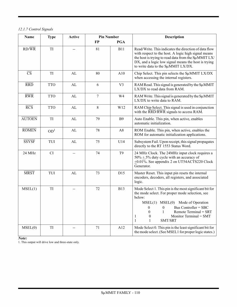
12.1.7 Control Signals
Note:1. This output will drive low and three-state only.
Name Type Active Pin Number FP PGA
Description
RD/WR TI -- 81 B11 Read/Write. This indicates the direction of data flow with respect to the host. A logic high signal means the host is trying to read data from the SIT LX/DX, and a logic low signal means the host is trying to write data to the SIT LX/DX.
CS TI AL 80 A10 Chip Select. This pin selects the SIT LX/DX when accessing the internal registers.
RRD TTO AL 6 V3 RAM Read. This signal is generated by the SIT LX/DX to read data from RAM.
RWR TTO AL 7 W4 RAM Write. This signal is generated by the SIT LX/DX to write data to RAM.
RCS TTO AL 8 W12 RAM Chip Select. This signal is used in conjunction with the RRD/RWR signals to access RAM.
AUTOEN TI AL 79 B9 Auto Enable. This pin, when active, enables automatic initialization.
ROMEN OD1 AL 78 A8 ROM Enable. This pin, when active, enables the ROM for automatic initialization applications.
SSYSF TUI AL 75 U14 Subsystem Fail. Upon receipt, this signal propagates directly to the RT 1553 Status Word.
24 MHz CI -- 74 T9 24 MHz Clock. The 24MHz input clock requires a 50% + 5% duty cycle with an accuracy of +0.01%. See appendix 2 on UT54ACTS220 Clock Generator.
MRST TUI AL 73 D15 Master Reset. This input pin resets the internal encoders, decoders, all registers, and associated logic.
MSEL(1) TI -- 72 B13 Mode Select 1. This pin is the most significant bit for the mode select. For proper mode selection, see below: MSEL(1) MSEL(0) Mode of Operation 0 0 Bus Controller = SBC
0 1 Remote Terminal = SRT 1 0 Monitor Terminal = SMT 1 1 SMT/SRT
MSEL(0) TI -- 71 A12 Mode Select 0. This pin is the least significant bit for the mode select. (See MSEL1 for proper logic states.)
SMMIT FAMILY - 110
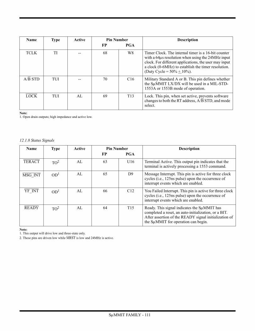
Note:1. Open drain outputs; high impedance and active low.
12.1.8 Status Signals
Note:1. This output will drive low and three-state only.2. These pins are driven low while MRST is low and 24MHz is active.
Name Type Active Pin Number FP PGA
Description
TCLK TI -- 68 W8 Timer Clock. The internal timer is a 16-bit counter with a 64s resolution when using the 24MHz input clock. For different applications, the user may input a clock (0-6MHz) to establish the timer resolution. (Duty Cycle = 50% + 10%).
A/B STD TUI -- 70 C16 Military Standard A or B. This pin defines whether the SIT LX/DX will be used in a MIL-STD-1553A or 1553B mode of operation.
LOCK TUI AL 69 T13 Lock. This pin, when set active, prevents software changes to both the RT address, A/B STD, and mode select.
Name Type Active Pin Number FP PGA
Description
TERACT TO2 AL 63 U16 Terminal Active. This output pin indicates that the terminal is actively processing a 1553 command.
MSG_INT OD1 AL 65 D9 Message Interrupt. This pin is active for three clock cycles (i.e., 125ns pulse) upon the occurrence of interrupt events which are enabled.
YF_INT OD1 AL 66 C12 You Failed Interrupt. This pin is active for three clock cycles (i.e., 125ns pulse) upon the occurrence of interrupt events which are enabled.
READY TO2 AL 64 T15 Ready. This signal indicates the SIT has completed a reset, an auto-initialization, or a BIT. After assertion of the READY signal initialization of the SIT for operation can begin.
SMMIT FAMILY - 111

SMMIT FAMILY - 112
12.1.9 Power/GroundThe following shows the package location of all power and ground pins associated with the SMMIT LXE\DXE.
Note:1. The VEE pins are not connected in the 5-Volt only SMMIT LXE/DXE.
Pin Number Pin Number FP PGA
Description
VDD 9, 60, 62, 76, 99, 100 C4, U4, B1, D7, T5, W10 +5 Volt Logic Power (+10%)
VCC 30, 35, 36, 39, 40, 45 D19, T19, C24, U24 LXE: +5 Volt Transceiver Power (+10%, -5%)Recommended de-coupling capacitors:>4.7F and .1FDXE: +5 Volt Transceiver Power (+10%)Recommended de-coupling capacitors; >4.7F and .1F
VEE1 27, 28, 47, 48 T21, T23, D21, D23 (LX only) -12 or -15 Volt Transceiver Power
(+5%)Recommended de-coupling capacitors:>4.7F and .1F
VSS 5, 10, 61, 67, 77, 98 C8, U8, D5, D11, T11, V1 Digital Ground
GND 29, 31, 34, 37, 38, 41, 44, 46 T17, U20, W24, D17, C20, A24 Transceiver Ground

13.0 SMMIT XTE PIN IDENTIFICATION AND DESCRIPTION
Figure 32. SMMIT XTE Functional Pin Diagram
A(15:0)
DA(15:0)
ALE
RD
R/WR or WR
CSDS
RDY
EA(12:0)
ED(7:0)
ECS
EC(2:0)
YF_INT
MSG_INT
YF_ACK
MSG_ACK
MSEL(5:0)
A/B STD
AUTOEN
LOCK
RTA(4:0)
RTPTY
CHA
CHA
CHB
CHB
TRST
TCK
JTAG (2:0)
TERACT
READY
BIST
SSYSF
24MHz
TCLK
MRST
VDD
VSS
GND
VCC
VEE (XT15, XT12)
PROCESSORINTERFACE
AUTO-INITIALIZATION
BUS
INTERRUPTS
MODE OFOPERATION
REMOTETERMINAL
ADDRESS
1553INTERFACE
JTAGPORT
STATUSOUTPUTS
SUBSYSTEMFAIL
CLOCKS
MASTERRESET
POWER&
GROUND
UT69151SMMIT
XTE
SMMIT FAMILY - 113
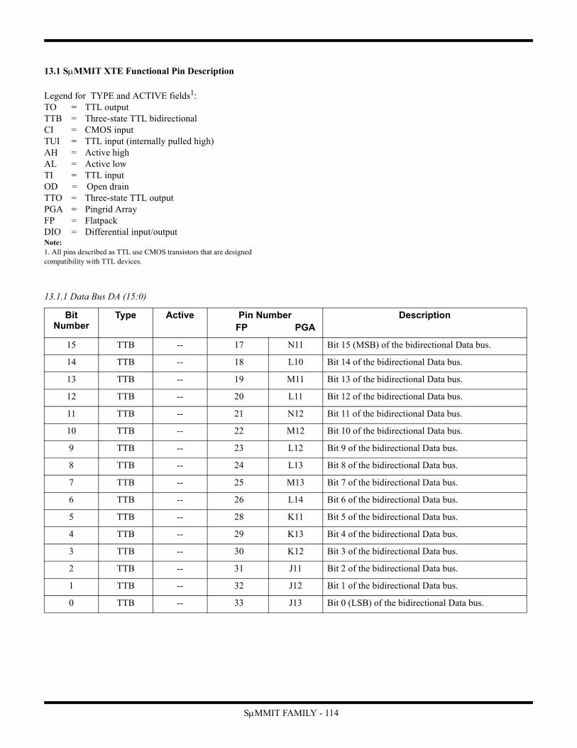
13.1 SMMIT XTE Functional Pin Description
Legend for TYPE and ACTIVE fields1:TO = TTL outputTTB = Three-state TTL bidirectionalCI = CMOS inputTUI = TTL input (internally pulled high)AH = Active highAL = Active lowTI = TTL inputOD = Open drainTTO = Three-state TTL outputPGA = Pingrid ArrayFP = FlatpackDIO = Differential input/outputNote:1. All pins described as TTL use CMOS transistors that are designed compatibility with TTL devices.
13.1.1 Data Bus DA (15:0)
Bit Number
Type Active Pin Number FP PGA
Description
15 TTB -- 17 N11 Bit 15 (MSB) of the bidirectional Data bus.
14 TTB -- 18 L10 Bit 14 of the bidirectional Data bus.
13 TTB -- 19 M11 Bit 13 of the bidirectional Data bus.
12 TTB -- 20 L11 Bit 12 of the bidirectional Data bus.
11 TTB -- 21 N12 Bit 11 of the bidirectional Data bus.
10 TTB -- 22 M12 Bit 10 of the bidirectional Data bus.
9 TTB -- 23 L12 Bit 9 of the bidirectional Data bus.
8 TTB -- 24 L13 Bit 8 of the bidirectional Data bus.
7 TTB -- 25 M13 Bit 7 of the bidirectional Data bus.
6 TTB -- 26 L14 Bit 6 of the bidirectional Data bus.
5 TTB -- 28 K11 Bit 5 of the bidirectional Data bus.
4 TTB -- 29 K13 Bit 4 of the bidirectional Data bus.
3 TTB -- 30 K12 Bit 3 of the bidirectional Data bus.
2 TTB -- 31 J11 Bit 2 of the bidirectional Data bus.
1 TTB -- 32 J12 Bit 1 of the bidirectional Data bus.
0 TTB -- 33 J13 Bit 0 (LSB) of the bidirectional Data bus.
SMMIT FAMILY - 114

13.1.2 Address Bus A(15:0)
13.1.3 Auto-initialization Address Bus EA(12:0)
Bit Number
Type Active Pin Number FP PGA
Description
15 TI -- 38 J14 Bit 15 (MSB) of the Address bus.
14 TI -- 39 H11 Bit 14 of the Address bus.
13 TI -- 40 H12 Bit 13 of the Address bus.
12 TI -- 41 H13 Bit 12 of the Address bus.
11 TI -- 42 G11 Bit 11 of the Address bus.
10 TI -- 43 G12 Bit 10 of the Address bus.
9 TI -- 45 G13 Bit 9 of the Address bus.
8 TI -- 46 G14 Bit 8 of the Address bus.
7 TI -- 47 F11 Bit 7 of the Address bus.
6 TI -- 48 F12 Bit 6 of the Address bus.
5 TI -- 49 F13 Bit 5 of the Address bus.
4 TI -- 50 D13 Bit 4 of the Address bus.
3 TI -- 51 E13 Bit 3 of the Address bus.
2 TI -- 52 C13 Bit 2 of the Address bus.
1 TI -- 54 E14 Bit 1 of the Address bus.
0 TI -- 55 C14 Bit 0 (LSB) of the Address bus.
Bit Number
Type Active Pin Number FP PGA
Description
12 TO -- 85 F9 Bit 12 (MSB) of the auto-init Address bus.
11 TO -- 84 F10 Bit 11 of the auto-init Address bus.
10 TO -- 83 G10 Bit 10 of the auto-init Address bus.
9 TO -- 82 C11 Bit 9 of the auto-init Address bus.
8 TO -- 81 G9 Bit 8 of the auto-init Address bus.
7 TO -- 80 E11 Bit 7 of the auto-init Address bus.
6 TO -- 79 E10 Bit 6 of the auto-init Address bus.
5 TO -- 78 E9 Bit 5 of the auto-init Address bus.
4 TO -- 77 G8 Bit 4 of the auto-init Address bus.
3 TO -- 76 H8 Bit 3 of the auto-init Address bus.
2 TO -- 75 J7 Bit 2 of the auto-init Address bus.
1 TO -- 74 J9 Bit 1 of the auto-init Address bus.
0 TO -- 73 J10 Bit 0 (LSB) of the auto-init Address bus.
SMMIT FAMILY - 115

13.1.4 Auto-initialization Data Bus ED(7:0)
13.1.5 Remote Terminal Address Inputs
Bit Number
Type Active Pin Number FP PGA
Description
7 TUI -- 68 K10 Bit 7 (MSB) of the auto-init data.
6 TUI -- 67 M7 Bit 6 of the auto-init data.
5 TUI -- 66 N3 Bit 5 of the auto-init data.
4 TUI -- 65 N8 Bit 4 of the auto-init data.
3 TUI -- 64 M8 Bit 3 of the auto-init data.
2 TUI -- 63 L8 Bit 2 of the auto-init data.
1 TUI -- 62 N9 Bit 1 of the auto-init data.
0 TUI -- 61 M9 Bit 0 (LSB) of the auto-init data.
Name Type Active Pin Number FP PGA
Description
RTA4 TUI -- 115 E2 Remote Terminal Address 4. This is the most significant bit for the RT address.
RTA3 TUI -- 116 G3 Remote Terminal Address 3. This is bit 3 of the RT address.
RTA2 TUI -- 117 F3 Remote Terminal Address 2. This is bit 2 of the RT address.
RTA1 TUI -- 118 G2 Remote Terminal Address 1. This is bit 1 of the RT address.
RTA0 TUI -- 119 F2 Remote Terminal Address 0. This input is the least significant bit of the RT address.
RTPTY TUI -- 120 G1 Remote Terminal Parity. This is an odd parity input for the RT address.
SMMIT FAMILY - 116

13.1.6 JTAG Testability Pins
13.1.7 Biphase Inputs/Outputs
Name Type Active Pin Number FP PGA
Description
NC -- -- 59 N10 Formerly MMU TDOM; now no connect.
VSS -- -- 58 L9 Formerly MMU TDIM; now tied to VSS.
VSS -- -- 57 M10 Formerly MMU TMSM; now tied to VSS.
TDO TTO -- 134 K3 SMMIT TDO. This input performs the operation of Test Data Output as defined in IEEE Standard 1149.1.
TDI TUI -- 135 K2 SMMIT TDI. This input performs the operation of Test Data Input as defined in IEEE Standard 1149.1.
TMS TUI -- 136 J2 SMMIT TMS. This input performs the operation of Test Mode Select as defined in IEEE Standard 1149.1.
TCK TI -- 137 L2 TCK. This input performs the operation of Test Clock as defined in IEEE Standard 1149.1. Can operate up to 1MHz.
TRST TUI AL 133 L3 TRST. This input provides the RESET to the TAP controller as defined in the IEEE Standard 1149.1. This non-inverting input buffer is optimized for driving TTL input levels. When not exercising JTAG , tie TRST to a logical 0.
Name Type Active Pin Number FP PGA
Description
CHA DIO -- 92 B7 Channel A (True). This is the Manchester-encoded true signal for Channel A.
CHA DIO -- 93 A7 Channel A (Complement). This is the Manchester-encoded complement signal for Channel A.
CHB DIO -- 102 A3 Channel B (True). This is the Manchester-encoded true signal for Channel B.
CHB DIO -- 103 A2 Channel B (Complement). This is the Manchester-encoded complement signal for Channel B.
SMMIT FAMILY - 117
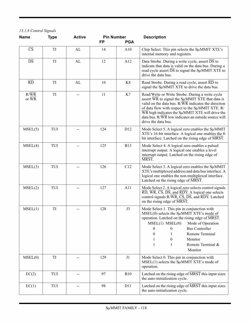
13.1.8 Control Signals
Name Type Active Pin Number DescriptionFP PGA
CS TI AL 14 A10 Chip Select. This pin selects the SMMIT XTE’s internal memory and registers.
DS TI AL 12 A12 Data Strobe. During a write cycle, assert DS to indicate that data is valid on the data bus. During a read cycle assert DS to signal the SMMIT XTE to drive the data bus.
RD TI AL 10 K8 Read Strobe. During a read cycle, assert RD to signal the SMMIT XTE to drive the data bus.
R/WR or WR
TI -- 11 K7 Read/Write or Write Strobe. During a write cycle assert WR to signal the SMMIT XTE that data is valid on the data bus. R/WR indicates the direction of data flow with respect to the SMMIT XTE. R/WR high indicates the SMMIT XTE will drive the data bus. R/WR low indicates an outside source will drive the data bus.
MSEL(5) TUI -- 124 D12 Mode Select 5. A logical zero enables the SMMIT XTE’s 16-bit interface. A logical one enables the 8-bit interface. Latched on the rising edge of MRST.
MSEL(4) TUI -- 125 B13 Mode Select 4. A logical zero enables a pulsed interrupt output. A logical one enables a level interrupt output. Latched on the rising edge of MRST.
MSEL(3) TUI -- 126 C12 Mode Select 3. A logical zero enables the SMMIT XTE’s multiplexed address and data bus interface. A logical one enables the non-multiplexed interface. Latched on the rising edge of MRST.
MSEL(2) TUI -- 127 A11 Mode Select 2. A logical zero selects control signals RD, WR, CS, DS, and RDY. A logical one selects control signals R/WR, CS, DS, and RDY. Latched on the rising edge of MRST.
MSEL(1) TI -- 128 J3 Mode Select 1. This pin in conjunction with MSEL(0) selects the SMMIT XTE’s mode of operation. Latched on the rising edge of MRST. MSEL(1) MSEL(0) Mode of Operation 0 0 Bus Controller 0 1 Remote Terminal 1 0 Monitor 1 1 Remote Terminal & Monitor
MSEL(0) TI -- 129 J1 Mode Select 0. This pin in conjunction with MSEL(1) selects the SMMIT XTE’s mode of operation.
EC(2) TUI -- 97 B10 Latched on the rising edge of MRST this input sizes the auto-initialization cycle.
EC(1) TUI -- 98 D11 Latched on the rising edge of MRST this input sizes the auto-initialization cycle.
SMMIT FAMILY - 118

EC(0) TUI -- 99 B12 Latched on the rising edge of MRST this input sizes the auto-initialization cycle.
24 MHz CI -- 7 N7 24 MHz Clock. The 24MHz input clock requires a 50% 5% duty cycle with an accuracy of 0.01%.
MRST TUI AL 130 J8 Master Reset. This input pin resets the internal encoder, decoder, all registers, and associated logic.
ALE TI AH 13 E12 Address Latch Enable. The falling edge of this strobe latches address information into the SMMIT XTE when operating with a multiplexed address and data bus.
TCLK TI -- 138 L7 Timer Clock. The internal timer is a 16-bit counter with a 64s resolution when using the 24MHz input clock. For applications requiring a different resolution, the user may input a clock from 0 to 6MHz to establish the timer resolution. (Duty cycle equals 50% 10%).
A/B STD TUI -- 122 H2 A/B. Military Standard A or B. This pin defines whether the SMMIT XTE operates per MIL-STD-1553A or MIL-STD-1553B. Input is latched on the rising edge of MRST.
LOCK TUI AL 121 H3 Lock. A logical zero applied to this pin prevents software from changing the RT address, A/B STD, or mode of operation. Input is latched on the rising edge of MRST.
AUTOEN TUI AL 131 M2 Auto Enable. When active this pin enables the SMMIT XTE’s auto-initialization function. Input is latched on the rising edge of MRST.
YF_ACK TUI AL 3 H9 You Failed Interrupt Acknowledge. Assertion of this input resets interrupt output YF_INT when operating in the level mode.
MSG_ACK TUI AL 5 K9 Message Interrupt Acknowledge. Assertion of this input resets interrupt output MSG_INT when operating in the level mode.
SSYSF TUI AL 113 D1 Subsystem Fail. Upon assertion, this signal propagates directly to the RT’s 1553 Status Word.
Name Type Active Pin Number DescriptionFP PGA
SMMIT FAMILY - 119

13.1.9 Status Signals
NOTE:1. This output will drive low and three-state only.2. These pins are driven high while MRST is low and 24MHZ is active.
13.1.10 Power/GroundThe following shows the package location of all power and ground pins associated with the SMMIT XTE.
Note:1. The VEE pins are not connected in the 5-Volt only SMMIT XTE.
Name Type Active Pin Number FP PGA
Description
YF_INT OD1 AL 4 M3 You Failed Interrupt. This pin asserts upon the occurrence of interrupt events which are not masked. Either a level output or pulse output.
MSG_INT OD1 AL 6 L1 Message Interrupt. This pin asserts upon the occurrence of interrupt events which are not masked. Either a level output or pulse output.
READY TO2 AL 110 D9 READY. Assertion of this output indicates the SMMIT XTE has completed initialization or BIT, and regular operation may begin.
ECS TO AL 96 B11 Chip Select. Auto-initialization device select.
RDY TTO AL 15 H10 Access Ready. Assertion of this output indicates that the host can complete the SMMIT XTE access.
TERACT TO2 AL 111 F7 TERACT. This output indicates that the terminal is actively processing a 1553 command.
BIST TTO AL 114 D10 Built-In Test. Assertion of this output indicates the SMMIT XTE is performing an internal memory test.
Pin Number Pin Number FP PGA
Description
VDD 2, 9, 16, 34, 37, 44, 60, 69, 72, 139
A8, B3, B14, F1, F14, G7, K1, K14, N2, N13
+5 Volt Logic Power (10%)
VCC CHA: 87, 94CHB: 101, 107
CHA: C9, C10, E8CHB: C1, D3, F8
XT15 & XT12: +5 Volt Transceiver Power (+10%,-5%)Recommended de-coupling capacitors: 47F (tantalum), .1F (ceramic) and .01F (ceramic)XT5: +5 Volt Transceiver Power (+10%)Recommended de-coupling capacitors: 47F (tantalum), .1F (ceramic) and .01F (ceramic)
VEE1 CHA: 86, 91
CHB: 100, 104CHA: D7, D8CHB: C2, D2
XT15 & XT12: -12 or -15 Volt Transceiver Power (5%)
VSS 1, 27, 35, 36, 53, 70, 71, 123, 132, 140
A9, A13, B2, B8, D14, H1, H7, H14, M1, M14
Digital Ground
GND CHA: 88, 89, 90, 95CHB: 105, 106, 108, 112
CHA: B9, C7, C8, E7CHB: B1, C3, E1, E3
Transceiver Ground
SMMIT FAMILY - 120

SMMIT FAMILY - 120
13.1.9 Status Signals
NOTE:1. This output will drive low and three-state only.2. These pins are driven high while MRST is low and 24MHZ is active.
13.1.10 Power/GroundThe following shows the package location of all power and ground pins associated with the SMMIT XTE.
Note:1. The VEE pins are not connected in the 5-Volt only SMMIT XTE.
Name Type Active Pin Number FP PGA
Description
YF_INT OD1 AL 4 M3 You Failed Interrupt. This pin asserts upon the occurrence of interrupt events which are not masked. Either a level output or pulse output.
MSG_INT OD1 AL 6 L1 Message Interrupt. This pin asserts upon the occurrence of interrupt events which are not masked. Either a level output or pulse output.
READY TO2 AL 110 D9 READY. Assertion of this output indicates the SMMIT XTE has completed initialization or BIT, and regular operation may begin.
ECS TO AL 96 B11 Chip Select. Auto-initialization device select.
RDY TTO AL 15 H10 Access Ready. Assertion of this output indicates that the host can complete the SMMIT XTE access.
TERACT TO2 AL 111 F7 TERACT. This output indicates that the terminal is actively processing a 1553 command.
BIST TTO AL 114 D10 Built-In Test. Assertion of this output indicates the SMMIT XTE is performing an internal memory test.
Pin Number Pin Number FP PGA
Description
VDD 2, 9, 16, 34, 37, 44, 60, 69, 72, 139
A8, B3, B14, F1, F14, G7, K1, K14, N2, N13
+5 Volt Logic Power (10%)
VCC CHA: 87, 94CHB: 101, 107
CHA: C9, C10, E8CHB: C1, D3, F8
XT15 & XT12: +5 Volt Transceiver Power (+10%,-5%)Recommended de-coupling capacitors: >4.7F (tantalum), .1F (ceramic) and .01F (ceramic)XT5: +5 Volt Transceiver Power (+10%)Recommended de-coupling capacitors: >4.7F (tantalum), .1F (ceramic) and .01F (ceramic)
VEE1 CHA: 86, 91
CHB: 100, 104CHA: D7, D8CHB: C2, D2
XT15 & XT12: -12 or -15 Volt Transceiver Power (5%)
VSS 1, 27, 35, 36, 53, 70, 71, 123, 132, 140
A9, A13, B2, B8, D14, H1, H7, H14, M1, M14
Digital Ground
GND CHA: 88, 89, 90, 95CHB: 105, 106, 108, 112
CHA: B9, C7, C8, E7CHB: B1, C3, E1, E3
Transceiver Ground

14.0 SMMIT E ABSOLUTE MAXIMUM RATINGS 1
(Referenced to VSS)
Note:1. Stresses outside the listed absolute maximum ratings may cause permanent damage to the device. This is a stress rating only, and functional operation of the device at these or any other conditions beyond limits indicated in the operational sections of this specification is not recommended. Exposure to absolute maximum rating conditions for extended periods may affect device reliability.
15.0 SMMIT E RECOMMENDED OPERATING CONDITIONS
SYMBOL PARAMETER LIMIT UNIT
VDD DC supply voltage -0.3 to 7.0 V
VI/O Voltage on any pin -.3 to VDD +.3 V
TSTG Storage temperature -65 to +150 C
TJ Maximum junction temperature +150 C
II DC input current +10 mA
TS Lead temperature(soldering, 5 seconds)
+300 C
JC Thermal resistance,junction-to-case
7 C/W
PD Maximum power dissipation 2.5 W
SYMBOL PARAMETER LIMIT UNIT
VDD DC supply voltage 4.5 to 5.5 V
TC Temperature range -55 to +125 C
VIN DC input voltage 0 to VDD V
FIN Operating frequency 24 + .01% MHz
DC Duty cycle 50 + 5 %
SMMIT FAMILY - 122

16.0 SMMIT E DC ELECTRICAL CHARACTERISTICS(VDD = 5.0V+10%; VSS = 0V 1; -55C < TC < +125C)
Notes: 1. Maximum allowable relative shift = 50mV.2. 24MHz input only.3. Supplied as a design limit but not guaranteed or tested.4. Not more than one output may be shorted at a time for maximum duration of one second.5. Capacitance measured for initial qualification or design changes which may affect the value.6. All inputs tied to VDD.7. Guaranteed by characterization, not tested.
SYMBOL PARAMETER CONDITION MIN MAX UNIT
VIL1 Low-level input voltage .8 V
VIL2 Low-level input voltageTCK input only
.7 V
VIH High-level input voltage 2.2 V
VILC Low-level input voltage 2 .3VDD V
VIHC High-level input voltage 2 .7VDD V
IIN Input leakage currentTTL driven inputsInputs with pull-up resistorsInputs with pull-up resistors
VIN = VDD or VSSVIN = VDD
VIN = VSS
-10-10
-167
1010-27
A
VOL Low-level output voltageTTL output loadsSingle-drive bufferCMOS output loads
IOL = 4.0mA
IOL = 1.0A7
.40.05
V
VOH High-level output voltageTTL output loadsSingle-drive bufferCMOS output loads
IOH = -4.0mA
IOH = -1.0A7
2.4VDD-0.05
V
IOZ Three-state output leakage currentTTL output loadsSingle-drive buffer VO = VDD or VSS -10 +10 A
IOS Short-circuit output current 3,4
TTL output loadsSingle-drive buffer
VDD = 5.5V, VO = 0VVDD = 5.5V, VO = VDD
-100 +100 mA
CIN Input capacitance 5 = 1MHz @ 0V 15 pF
COUT Output capacitance 5
Single-drive buffer
= 1MHz @ 0V 15 pF
CIO Bidirectional capacitance 5 = 1MHz @ 0V 25 pF
QIDD Quiescent current 6 = 0MHz - Non-RadHard, RadHard 100KRadHard 300K
= 0MHz (TC = 25oC)
15
35
mAmAA
SIDD Standby operating current = 24MHz MRST=VDD 40 mA
MRST=VSS7 260
SMMIT FAMILY - 123

SµMMIT FAMILY - 124
17.0 SµMMIT LXE/DXE & SµMMIT XTE ABSOLUTE MAXIMUM RATINGS 1(Referenced to VSS)
Note:1. Stress outside the listed absolute maximum rating may cause permanent damage to the device. This is a stress rating only, and functional operation of the device at these or any other conditions beyond limits indicated in the operational sections of this specification is not recommended. Exposure to absolute maximum rating conditions for extended periods may affect device reliability. 2. Mounting per MIL-STD-883, Method 1012.
SYMBOL PARAMETER LIMIT UNIT
VDD Logic supply voltage -0.3 to 7.0 V
PD Maximum power dissipation 5 W
VEE Transceiver supply voltage LXE, XTE15 & XTE12 -22 V
VCC Transceiver supply voltage DXE, XTE5 -0.3 to 7.0 V
VDR Input voltage range (receiver) LXE, XTE15 & XTE12
DXE, XTE54210
VP, L-LVP, L-L
VI/O Logic voltage on any pin -.3 to VDD +.3 V
II Logic input current ±10 mA
IO Peak output current (transmitter) LXE, XTE15 & XTE12
DXE, XTE5190
1000mAmA
TSTG Storage temperature -65 to +150 °C
TJ Maximum junction temperature LXE, XTE15 & XTE12
DXE, XTE5+150+150
°C
TS Lead temperature(soldering, 5 seconds)
+300 °C
TC Operating temperature case -55 to + 125 °C
ΘJC Thermal resistance,junction-to-case 2
7 °C/W

SµMMIT FAMILY - 125
18.0 SµMMIT LXE/DXE & SµMMIT XTE RECOMMENDED OPERATING CONDITIONS
SYMBOL PARAMETER LIMIT UNIT
VCC Transceiver supply voltage rangeLXE, XTE15 & XTE12DXE, XTE5
4.75 to 5.54.5 to 5.5
V
VDD Logic supply voltage 4.5 to 5.5 V
VEE Transceiver supply voltage range LXE, XTE15 & XTE12 -12 or -15
(±5%)
V
VDR Receiver differential voltageLXE, XTE15 & XTE12DXE, XTE5
408.0
VP-P
VIN Logic DC input voltage 0 to VDD V
VIC Receiver common mode input voltage rangeLXE, XTE15 & XTE12DXE, XTE5
±10±5.0
V
IO Driver peak output currentLXE, XTE15 & XTE12DXE, XTE5
180700
mA
SD Serial data rate 0 to 1 MHz
DC Clock Duty cycle 50 ± 5 %
TC Case operating temperature range -55 to + 125 °C
FIN Operating frequency 24 ± .01% MHz
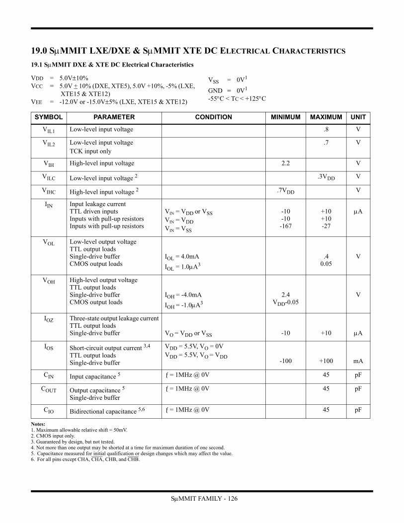
19.0 SMMIT LXE/DXE & SMMIT XTE DC ELECTRICAL CHARACTERISTICS
19.1 SMMIT DXE & XTE DC Electrical Characteristics
VDD = 5.0V10%VCC = 5.0V + 10% (DXE, XTE5), 5.0V +10%, -5% (LXE, XTE15 & XTE12)VEE = -12.0V or -15.0V5% (LXE, XTE15 & XTE12)
VSS = 0V1
GND = 0V1
-55C < TC < +125C
Notes: 1. Maximum allowable relative shift = 50mV.2. CMOS input only.3. Guaranteed by design, but not tested.4. Not more than one output may be shorted at a time for maximum duration of one second.5. Capacitance measured for initial qualification or design changes which may affect the value.6. For all pins except CHA, CHA, CHB, and CHB.
SYMBOL PARAMETER CONDITION MINIMUM MAXIMUM UNIT
VIL1 Low-level input voltage .8 V
VIL2 Low-level input voltageTCK input only
.7 V
VIH High-level input voltage 2.2 V
VILC Low-level input voltage 2 .3VDD V
VIHC High-level input voltage 2 .7VDD V
IIN Input leakage currentTTL driven inputsInputs with pull-up resistorsInputs with pull-up resistors
VIN = VDD or VSSVIN = VDDVIN = VSS
-10-10
-167
+10+10-27
A
VOL Low-level output voltageTTL output loadsSingle-drive bufferCMOS output loads
IOL = 4.0mA
IOL = 1.0A3
.40.05
V
VOH High-level output voltageTTL output loadsSingle-drive bufferCMOS output loads
IOH = -4.0mA
IOH = -1.0A3
2.4VDD-0.05
V
IOZ Three-state output leakage currentTTL output loadsSingle-drive buffer VO = VDD or VSS -10 +10 A
IOS Short-circuit output current 3,4
TTL output loadsSingle-drive buffer
VDD = 5.5V, VO = 0VVDD = 5.5V, VO = VDD
-100 +100 mA
CIN Input capacitance 5 = 1MHz @ 0V 45 pF
COUT Output capacitance 5
Single-drive buffer
= 1MHz @ 0V 45 pF
CIO Bidirectional capacitance 5,6 = 1MHz @ 0V 45 pF
SMMIT FAMILY - 126

SMMIT FAMILY - 127
19.2 SMMIT LXE & XTE (15 & 12) DC Electrical Characteristics 1,2
VDD = 5.0V10%
VCC = 5.0V +10%, -5%
VEE = -12.0V or -15.0V5%
VSS = 0V1
GND = 0V1
-55C < TC < +125C
Notes: 1.Maximum allowable relative shift = 50mV.2. As specified in test conditions.3. All inputs tied to VDD.4. Guaranteed by characterization, not tested.
19.3 SMMIT DXE & XTE (5) DC Electrical Characteristics 1,2
VDD = 5.0V10%
VCC = 5.0V +10%
VSS = 0V1
GND = 0V1
-55C < TC < +125C
Notes: 1. Maximum allowable relative shift = 50mV.2. All inputs tied to VDD.3. Guaranteed by characterization, not tested.
SYMBOL PARAMETER CONDITION MINIMUM MAXIMUM UNIT
ICC VCC supply current VEE = -12V VCC = 5V 0% duty cycle (non-transmitting)50% duty cycle (ƒ = 1MHz)4
100% duty cycle (ƒ = 1MHz)4
VEE = -15V VCC = 5V 0% duty cycle (non-transmitting)50% duty cycle (ƒ = 1MHz)4
100% duty cycle (ƒ = 1MHz)4
140140140
140140140
mAmAmA
mAmAmA
IEE IEE supply current VEE = -12V VCC = 5V 0% duty cycle (non-transmitting)50% duty cycle (ƒ = 1MHz)4
100% duty cycle (ƒ = 1MHz)VEE = -15V VCC = 5V 0% duty cycle (non-transmitting)50% duty cycle (ƒ = 1MHz)4
100% duty cycle (ƒ = 1MHz)
80180270
80180270
mAmAmA
mAmAmA
QIDD Quiescent current 3 = 0MHz XT= 0MHz LX
20 1
mAmA
QIDD Quiescent current 3 = 0MHz LX
TC = 25oC
35 A
SIDD Standby operating current = 24MHz MRST = VDD 80 mA
MRST = VSS4 300 mA
SYMBOL PARAMETER CONDITION MINIMUM MAXIMUM UNIT
ICC VCC supply current 0% duty cycle (non-transmitting)25% duty cycle (ƒ = 1MHz) 3
50% duty cycle (ƒ = 1MHz) 3
87.5% duty cycle (ƒ = 1MHz)
55250410650
mAmAmAmA
QIDD Quiescent current 2 = 0MHz XT= 0MHz DX - Non-RadHard, RadHard 100K= 0MHz DX - RadHard 300K
20 15
mAmAmA
QIDD Quiescent current 2 = 0MHz DX, TC = 25oC 35 A
SIDD Standby operating current = 24MHz 40 mA
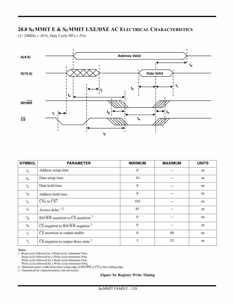
20.0 SMMIT E & SMMIT LXE/DXE AC ELECTRICAL CHARACTERISTICS(= 24MHz ± .01%, Duty Cycle 50% ± 5%)
Notes:1. Read cycle followed by a Read cycle -minimum 45ns.
Read cycle followed by a Write cycle-minimum 45ns.Write cycle followed by a Read cycle-minimum 85ns.Write cycle followed by a Write cycle-minimum 85ns.
2. Minimum pulse width from latter rising edge of RD/WR or CS to first falling edge.3. Guaranteed by characterization, but not tested.
SYMBOL PARAMETER MINIMUM MAXIMUM UNITS
ta Address setup time 0 -- ns
tb Data setup time 10 -- ns
tc Data hold time 8 -- ns
td Address hold time 8 -- ns
te CSto CS 105 -- ns
tf Access delay 1,2 85 -- ns
tg RD/WR assertion to CS assertion 3 0 -- ns
th CS negation to RD/WR negation 3 0 -- ns
ti CS assertion to output enable 0 40 ns
tj CS negation to output three-state 3 5 35 ns
A(4:0)
D(15:0)
RD/WR
CS
ta
tbtc
td
Data Valid
Address Valid
tf
te
ti
tj
thtg
Figure 34. Register Write Timing
SMMIT FAMILY - 128

Notes:1. Guaranteed by characterization, but not tested.2. Minimum pulse width from latter rising edge of RD/WR or CS to first falling edge.3. Read cycle followed by a Read cycle - minimum 45ns.
Read cycle followed by a Write cycle - minimum 45ns.Write cycle followed by a Read cycle - minimum 85ns.Write cycle followed by a Write cycle - minimum 85ns.
Figure 35. Register Read Timing
A(4:0)
D(15:0)
RD/WR
CS
ta
tb
tc
td
Address Valid
te
tf tg
Data Valid
SYMBOL PARAMETER MINIMUM MAXIMUM UNITS
ta Address setup time 0 -- ns
tb CS assertion to output enable data valid -- 95 ns
tc CS negation to output disabled 1 5 35 ns
td Address hold time 0 -- ns
te CS assertion to output enable data invalid 0 40 ns
tf Access delay 2,3 45 -- ns
tg CS to CS 105 -- ns
SMMIT FAMILY - 129

Notes:1. Pulse width duration is measured with respect to the SMMIT recognizing DTACK assertion.2. Guaranteed by characterization, but not tested.3. This timing diagram includes memory writes resulting from the SMMIT’s auto-initialization sequence.
Figure 36. Memory Write Timing3
SYMBOL PARAMETER MINIMUM MAXIMUM UNITS
ta Address propagation delay - RadHard - non-RadHard
00
1821
nsns
tb Address valid to RCS, RWR assertion 15 35 ns
tc DTACK setup time 10 -- ns
td RCS and RWR hold time 1 20 50 ns
te Data propagation delay 20 60 ns
tg Address hold time 10 30 ns
th DTACK hold time 10 -- ns
ti RWR and RCS pulse width (DTACK tied to ground)- RadHard- non-RadHard
3432
----
nsns
tj RWR and RCS to DMACK2 15 125 ns
tk Data hold time 2 10 40 ns
A(15:0)
D(15:0)
tetg
ta
24MHz
Data Valid
Address Valid
tk
RWR
RCS
DTACK
tb
tc th
td
ti
tj
DMACK
SMMIT FAMILY - 130

SMMIT FAMILY - 131
Notes:1. Pulse width duration is measured with respect to theSMMIT’s recognizing DTACK assertion.2. Guaranteed by characterization, but not tested.3. This timing diagram includes memory writes resulting from the SMMIT’s auto-initialization sequence.
Figure 37. Memory Read Timing3
SYMBOL PARAMETER MINIMUM MAXIMUM UNITS
ta Address propagation delay - RadHard - non-RadHard
00
1821
ns
tb Address valid to RCS, RRD assertion 15 35 ns
tc DTACK setup time 10 -- ns
td RCS and RRD hold time 1 20 50 ns
te Data setup delay - RadHard - non-RadHard
1410
----
nsns
tf Data hold delay - RadHard - non-RadHard
02
----
nsns
tg Address hold time 10 30 ns
th DTACK hold time 10 -- ns
ti RRD and RCS pulse width (DTACK tied to ground) - RadHard - non-RadHard
3432
----
nsns
tj RRD and RCS to DMACK2 15 45 ns
A(15:0)
D(15:0)
RRD
RCS
DTACK
tb
tc th
td
tg
ta
24MHz
Data Valid
ti
Address Valid
tfte
tj
DMACK

SMMIT FAMILY - 132
Note:1. Guaranteed by characterization, but not tested.
Figure 38. DMA Timing
TERACT
ta
tb
DMACK
A(15:0)
DMAR
DMAG
tc
te
tf
td
tg
th
tj
ti
RRD, RWR, RCS
Valid
SYMBOL PARAMETER MINIMUM MAXIMUM UNITS
ta TERACT assertion to DMAR assertion1 5 -- s
tb DMAR assertion to DMACK negation1
Bus ControllerRemote TerminalRemote Terminal and MonitorMonitor
--------
16 7 7 7
ssss
tc DMAG assertion to DMACK assertion - RadHard - non-RadHard
05
3030
nsns
td DMAG assertion to DMAR negation 1 0 35 ns
te DMACK assertion to address bus active - RadHard - non-RadHard
0-5
55
nsns
tf DMACK assertion to DMAG negation 10 -- ns
tg DMACK negation to DMAR assertion1 500 -- ns
th DMACK assertion to RAM control active (negated)- RadHard- non-RadHard
0-5
55
nsns
ti DMACK negation to A(15:0) three-state 1 -- 5 ns
tj DMACK negation to RAM control
disabled 1-- 5 ns

Note:1. SMMIT must receive at least 3 24MHz clock cycles before deassertion of MRST.2. Power-up Master Reset Timing with Auto-initialization enabled.3. Power-up Master Reset Timing with Auto-initialization disabled.4. Guaranteed by characterization, but not tested.
SYMBOL PARAMETER MINIMUM MAXIMUM UNITS
ta MRST pulse width4 500 -- ns
tb MRST negation to ROMEN assertion4 -- 5 s
tc MRST negation to READY assertion4 -- 10 s
td DMACK negation to ROMEN negation4 -- 500 ns
MRSTta
tb
tdROMEN2
DMACK2
AUTOEN2
READY2
24MHz1
AUTOEN3
READY3tc
Figure 39. Power-up Master Reset Timing
SMMIT FAMILY - 133

Note:1. Guaranteed by characterization, but not tested.
SYMBOL PARAMETER MINIMUM MAXIMUM UNITS
ta Biphase output skew -- 10 ns
tb Biphase input skew (low to high)1 -- 250 ns
tc Biphase input skew (high to low)1 -- 250 ns
td Biphase input pulse width1 250 -- ns
TA, TB
RA, RB
ta
TA, TB
RA, RB
tb tc
td
Figure 40. BiPhase Timing (SMMIT only)
SMMIT FAMILY - 134
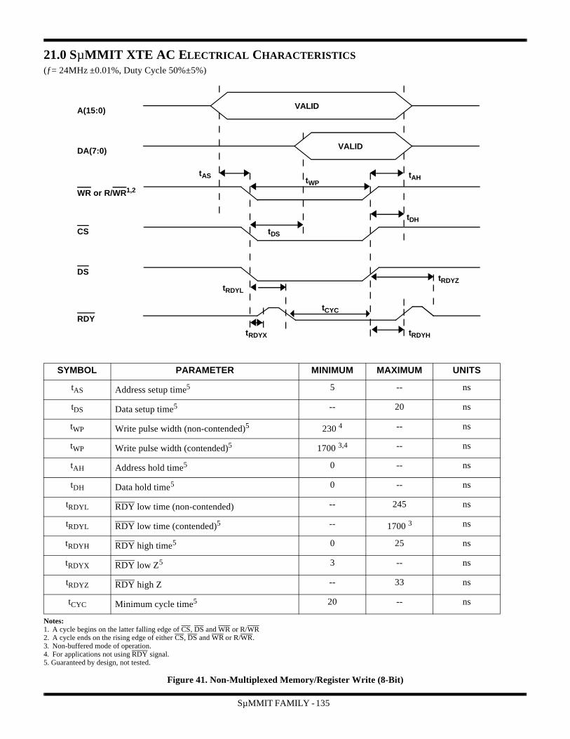
SµMMIT FAMILY - 135
21.0 SµMMIT XTE AC ELECTRICAL CHARACTERISTICS(ƒ= 24MHz ±0.01%, Duty Cycle 50%±5%)
Notes:1. A cycle begins on the latter falling edge of CS, DS and WR or R/WR2. A cycle ends on the rising edge of either CS, DS and WR or R/WR.3. Non-buffered mode of operation.4. For applications not using RDY signal.5. Guaranteed by design, not tested.
Figure 41. Non-Multiplexed Memory/Register Write (8-Bit)
SYMBOL PARAMETER MINIMUM MAXIMUM UNITS
tAS Address setup time5 5 -- ns
tDS Data setup time5 -- 20 ns
tWP Write pulse width (non-contended)5 230 4 -- ns
tWP Write pulse width (contended)5 1700 3,4 -- ns
tAH Address hold time5 0 -- ns
tDH Data hold time5 0 -- ns
tRDYL RDY low time (non-contended) -- 245 ns
tRDYL RDY low time (contended)5 -- 1700 3 ns
tRDYH RDY high time5 0 25 ns
tRDYX RDY low Z5 3 -- ns
tRDYZ RDY high Z -- 33 ns
tCYC Minimum cycle time5 20 -- ns
A(15:0)
DA(7:0)
CS
DS
RDY
WR or R/WR1,2
tAS
tDS
tWP
tRDYL
tDH
tAH
tRDYZ
tRDYX tRDYH
VALID
VALID
tCYC
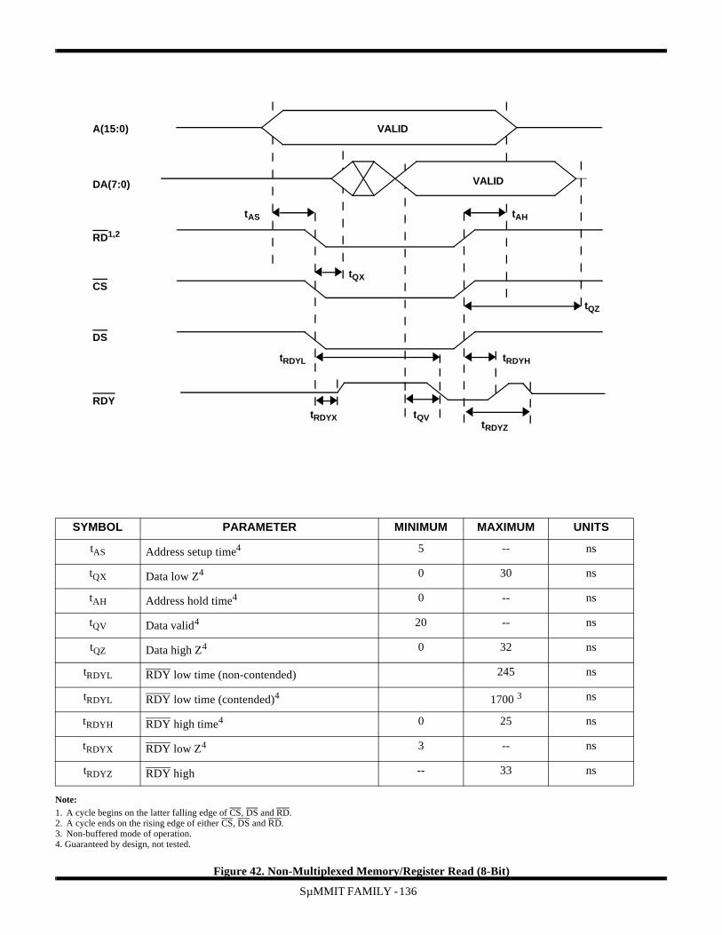
SµMMIT FAMILY - 136
Note:1. A cycle begins on the latter falling edge of CS, DS and RD.2. A cycle ends on the rising edge of either CS, DS and RD.3. Non-buffered mode of operation.4. Guaranteed by design, not tested.
Figure 42. Non-Multiplexed Memory/Register Read (8-Bit)
SYMBOL PARAMETER MINIMUM MAXIMUM UNITS
tAS Address setup time4 5 -- ns
tQX Data low Z4 0 30 ns
tAH Address hold time4 0 -- ns
tQV Data valid4 20 -- ns
tQZ Data high Z4 0 32 ns
tRDYL RDY low time (non-contended) 245 ns
tRDYL RDY low time (contended)4 1700 3 ns
tRDYH RDY high time4 0 25 ns
tRDYX RDY low Z4 3 -- ns
tRDYZ RDY high -- 33 ns
A(15:0)
DA(7:0)
CS
DS
RD1,2
tQV
VALID
VALID
tAS
tQX
tRDYL tRDYH
tQZ
tAH
RDYtRDYX
tRDYZ

SµMMIT FAMILY - 137
Notes: 1. A cycle begins on the latter falling edge of CS, DS and WR or R/WR.2. A cycle ends on the rising edge of either CS, DS and WR or R/WR.3. Non-buffered mode of operation.4. For applications not using RDY signal.5. Guaranteed by design, not tested.6. Guaranteed by device characterization, not tested.7. A15 must be tied low.
Figure 43. Non-Multiplexed Memory/Register Write (16-Bit)
SYMBOL PARAMETER MINIMUM MAXIMUM UNITS
tAS Address setup time6 5 -- ns
tDS Data setup time6 -- 20 ns
tWP Write pulse width (non-contended)5 230 4 -- ns
tWP Write pulse width (contended)5 1700 3,4 -- ns
tAH Address hold time6 0 -- ns
tDH Data hold time6 0 -- ns
tRDYL RDY low time (non-contended) -- 245 ns
tRDYL RDY low time (contended)5 -- 1700 3 ns
tRDYH RDY high time6 0 25 ns
tRDYX RDY low Z6 3 -- ns
tRDYZ RDY high Z -- 33 ns
tCYC Minimum cycle time5 20 -- ns
A(14:0)7
DA(15:0)
CS
DS
RDY
WR or R/WR1,2
tAS
tDS
tWP
tRDYL
tDH
tAH
tRDYZ
tRDYX tRDYH
VALID
VALID
tCYC

SµMMIT FAMILY - 138
Notes:1. A cycle begins on the latter falling edge of CS, DS and RD.2. A cycle ends on the rising edge of either CS, DS and RD.3. Non-buffered mode of operation.4. Guaranteed by design, not tested.5. Guaranteed by device characterization, not tested.6. A15 must be tied low.
Figure 44. Non-Multiplexed Memory/Register Read (16-Bit)
A(14:0)6
DA(15:0)
CS
DS
RD1,2
tQV
VALID
VALID
tAS
tQX
tRDYL tRDYH
tQZ
tAH
RDYtRDYX
tRDYZ
SYMBOL PARAMETER MINIMUM MAXIMUM UNITS
tAS Address setup time5 5 -- ns
tQX Data low Z5 0 30 ns
tAH Address hold time5 0 -- ns
tQV Data valid5 20 -- ns
tQZ Data high Z5 0 32 ns
tRDYL RDY low time (non-contended) -- 245 ns
tRDYL RDY low time (contended)4 -- 1700 3 ns
tRDYH RDY high time5 0 25 ns
tRDYX RDY low Z5 3 -- ns
tRDYZ RDY high Z -- 33 ns
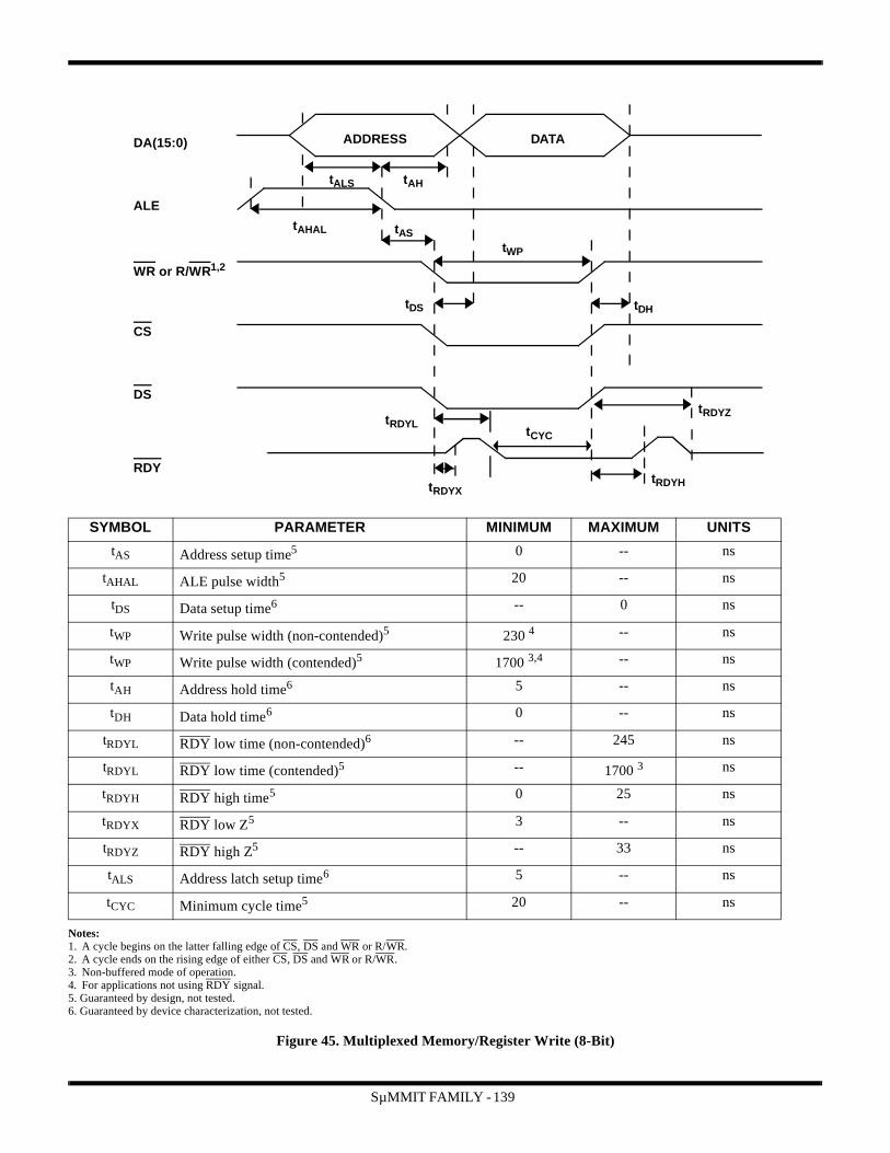
SµMMIT FAMILY - 139
Notes:1. A cycle begins on the latter falling edge of CS, DS and WR or R/WR.2. A cycle ends on the rising edge of either CS, DS and WR or R/WR.3. Non-buffered mode of operation.4. For applications not using RDY signal.5. Guaranteed by design, not tested.6. Guaranteed by device characterization, not tested.
Figure 45. Multiplexed Memory/Register Write (8-Bit)
SYMBOL PARAMETER MINIMUM MAXIMUM UNITS
tAS Address setup time5 0 -- ns
tAHAL ALE pulse width5 20 -- ns
tDS Data setup time6 -- 0 ns
tWP Write pulse width (non-contended)5 230 4 -- ns
tWP Write pulse width (contended)5 1700 3,4 -- ns
tAH Address hold time6 5 -- ns
tDH Data hold time6 0 -- ns
tRDYL RDY low time (non-contended)6 -- 245 ns
tRDYL RDY low time (contended)5 -- 1700 3 ns
tRDYH RDY high time5 0 25 ns
tRDYX RDY low Z5 3 -- ns
tRDYZ RDY high Z5 -- 33 ns
tALS Address latch setup time6 5 -- ns
tCYC Minimum cycle time5 20 -- ns
DA(15:0)
ALE
CS
DS
RDY
WR or R/WR1,2
tAH
tDS
tWP
tDH
DATAADDRESS
tAStAHAL
tRDYLtRDYZ
tRDYHtRDYX
tALS
tCYC

SµMMIT FAMILY - 140
Notes:1. A cycle begins on the latter falling edge of CS, DS and RD.2. A cycle ends on the rising edge of either CS, DS and RD.3. Non-buffered mode of operation.4. Guaranteed by design, not tested.
Figure 46. Multiplexed Memory/Register Read (8-Bit)
SYMBOL PARAMETER MINIMUM MAXIMUM UNITS
tAS Address setup time4 0 -- ns
tAHAL ALE pulse width4 20 -- ns
tQX Data low Z4 0 30 ns
tAH Address hold time 5 -- ns
tQV Data valid 12 -- ns
tQZ Data high Z 3 32 ns
tRDYL RDY low time (non-contended)4 -- 245 ns
tRDYL RDY low time (contended)4 -- 1700 3 ns
tRDYH RDY high time4 0 25 ns
tRDYX RDY low Z4 3 -- ns
tRDYZ RDY high Z4 -- 33 ns
tALS Address latch setup time4 5 -- ns
DA(15:0)
ALE
CS
DS
RDY
RD1,2
tRDYL
tQZ
tAH
ADDRESS DATA
tAHAL
tQX
tAS
tRDYH
tQVtRDYX
tRDYZ
tALS
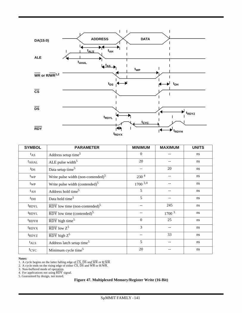
SµMMIT FAMILY - 141
Notes:1. A cycle begins on the latter falling edge of CS, DS and WR or R/WR2. A cycle ends on the rising edge of either CS, DS and WR or R/WR.3. Non-buffered mode of operation.4. For applications not using RDY signal.5. Guaranteed by design, not tested.
Figure 47. Multiplexed Memory/Register Write (16-Bit)
SYMBOL PARAMETER MINIMUM MAXIMUM UNITS
tAS Address setup time5 0 -- ns
tAHAL ALE pulse width5 20 -- ns
tDS Data setup time5 -- 20 ns
tWP Write pulse width (non-contended)5 230 4 -- ns
tWP Write pulse width (contended)5 1700 3,4 -- ns
tAH Address hold time5 5 -- ns
tDH Data hold time5 5 -- ns
tRDYL RDY low time (non-contended)5 -- 245 ns
tRDYL RDY low time (contended)5 -- 1700 3 ns
tRDYH RDY high time5 0 25 ns
tRDYX RDY low Z5 3 -- ns
tRDYZ RDY high Z5 -- 33 ns
tALS Address latch setup time5 5 -- ns
tCYC Minimum cycle time5 20 -- ns
DA(15:0)
ALE
CS
DS
RDY
WR or R/WR1,2
tAH
tDS
tWP
tRDYL
tRDYH
tDH
DATAADDRESS
tAStAHAL
tRDYX
tRDYZ
tALS
tCYC
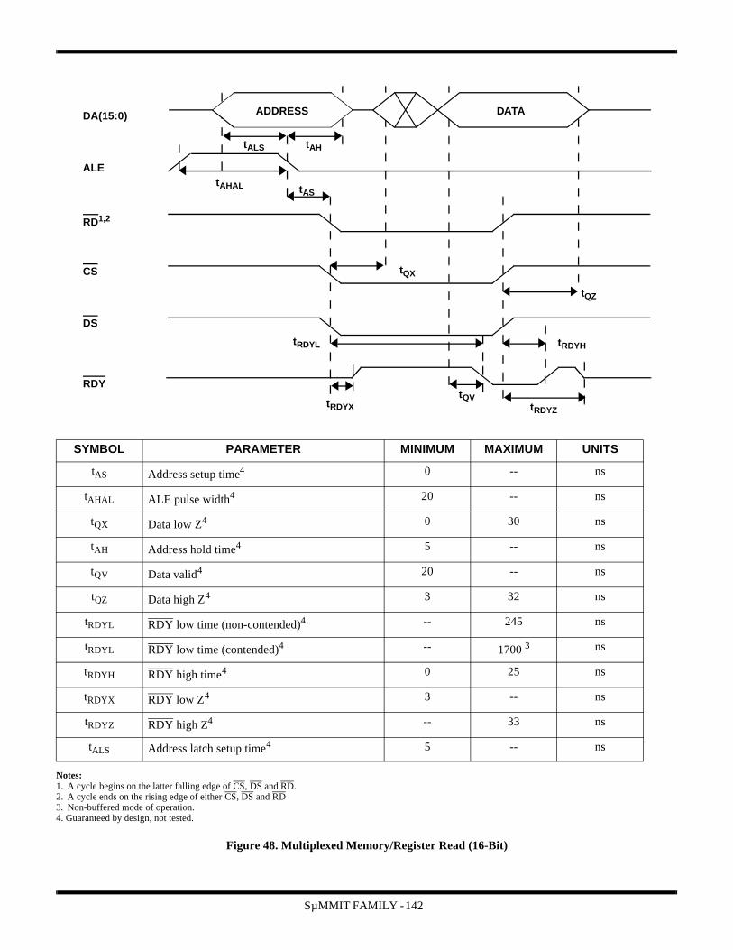
SµMMIT FAMILY - 142
Notes:1. A cycle begins on the latter falling edge of CS, DS and RD.2. A cycle ends on the rising edge of either CS, DS and RD3. Non-buffered mode of operation.4. Guaranteed by design, not tested.
Figure 48. Multiplexed Memory/Register Read (16-Bit)
SYMBOL PARAMETER MINIMUM MAXIMUM UNITS
tAS Address setup time4 0 -- ns
tAHAL ALE pulse width4 20 -- ns
tQX Data low Z4 0 30 ns
tAH Address hold time4 5 -- ns
tQV Data valid4 20 -- ns
tQZ Data high Z4 3 32 ns
tRDYL RDY low time (non-contended)4 -- 245 ns
tRDYL RDY low time (contended)4 -- 1700 3 ns
tRDYH RDY high time4 0 25 ns
tRDYX RDY low Z4 3 -- ns
tRDYZ RDY high Z4 -- 33 ns
tALS Address latch setup time4 5 -- ns
DA(15:0)
ALE
CS
DS
RDY
RD1,2
tAS
tRDYL tRDYH
tQZ
tAH
ADDRESS
tAHAL
tQX
tQVtRDYX tRDYZ
DATA
tALS

SµMMIT FAMILY - 143
Notes:1. Guaranteed by design, not tested.
Figure 49. Auto-Initialization Read Cycle
SYMBOL PARAMETER MINIMUM MAXIMUM UNITS
tAS Address setup time1 35 -- ns
tAH Address hold time1 35 -- ns
tDS Data setup time1 41 -- ns
tDH Data hold time1 5 -- ns
tRP Read pulse width1 160 -- ns
tS Setup time1 45 -- ns
EA(12:0)
ED(7:0)
ECS
tDS
tRP
tDH
tAH
EC(2:0)
MRST
tS
MSEL(5:0)
N N + 1
tDH
tAS
VALID VALID

SµMMIT FAMILY - 144
SYMBOL PARAMETER MINIMUM MAXIMUM UNITS
ta Maximum Register/Memory Time
Bus Controller1
Remote Terminal1
Remote Terminal and Monitor1
Monitor1
--------
16777
µsµsµsµs
Address BusA(15:0), A(14:0), DA(15:0), or DA(14:0)
Control Signals(DS, CS, RD, R/WR)
ADDRESS VALID
ta
Figure 50. Maximum Cycle Time Notes:1. Guaranteed by design, not tested.

SMMIT FAMILY - 145
SYMBOL PARAMETER MIN MAX UNITS
ta TCK frequency - 1 MHz
ta TCK period 1000 - ns
tb TCK high time 1/2ta - ns
tc TCK low time 1/2ta - ns
td TCK rise time - 5 ns
te TCK fall time - 5 ns
tf TDI, TMS setup time 250 - ns
tg TDI, TMS hold time 250 - ns
th TDO valid delay 250 - ns
Figure 51. JTAG Timing
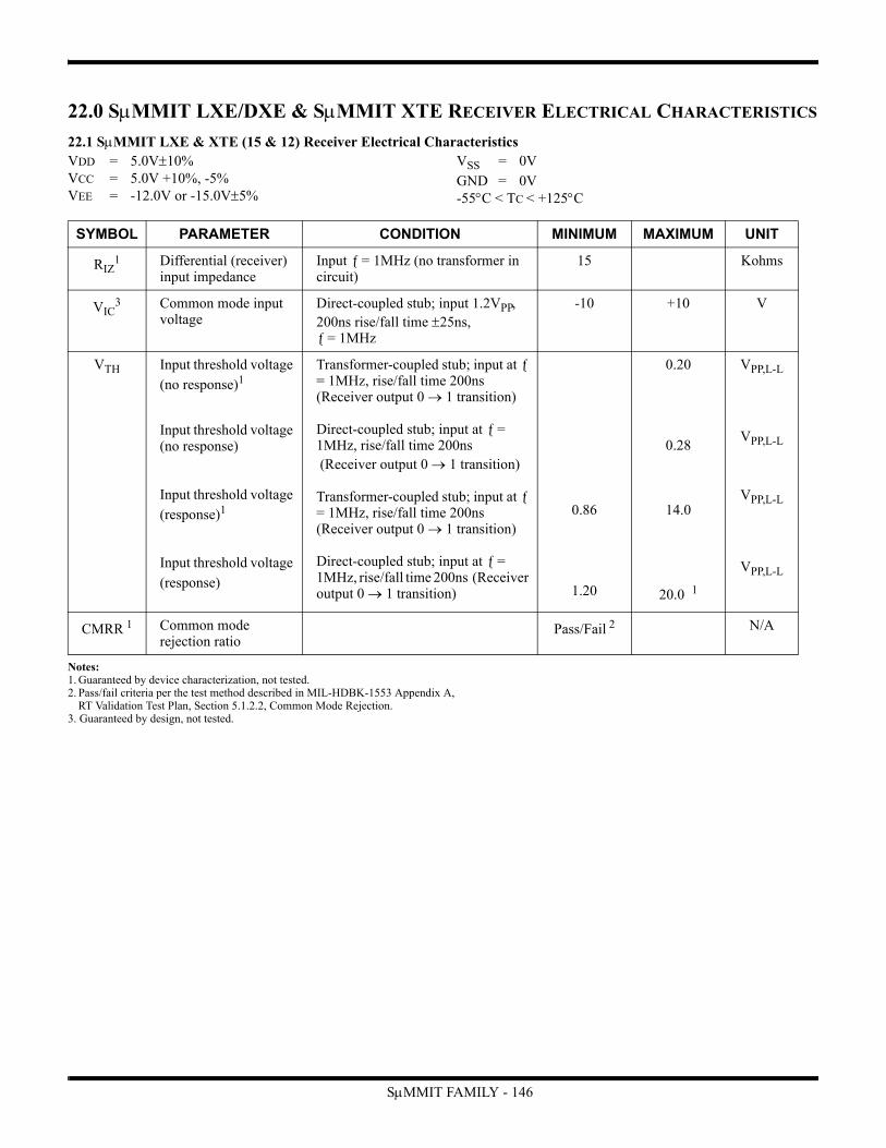
22.0 SMMIT LXE/DXE & SMMIT XTE RECEIVER ELECTRICAL CHARACTERISTICS
22.1 SMMIT LXE & XTE (15 & 12) Receiver Electrical CharacteristicsVDD = 5.0V10%VCC = 5.0V +10%, -5%VEE = -12.0V or -15.0V5%
VSS = 0V
GND = 0V-55C < TC < +125C
Notes:1. Guaranteed by device characterization, not tested.2. Pass/fail criteria per the test method described in MIL-HDBK-1553 Appendix A,
RT Validation Test Plan, Section 5.1.2.2, Common Mode Rejection.3. Guaranteed by design, not tested.
SYMBOL PARAMETER CONDITION MINIMUM MAXIMUM UNIT
RIZ1 Differential (receiver)
input impedanceInput = 1MHz (no transformer in circuit)
15 Kohms
VIC3 Common mode input
voltageDirect-coupled stub; input 1.2VPP, 200ns rise/fall time 25ns, = 1MHz
-10 +10 V
VTH Input threshold voltage
(no response)1
Input threshold voltage (no response)
Input threshold voltage
(response)1
Input threshold voltage
(response)
Transformer-coupled stub; input at = 1MHz, rise/fall time 200ns (Receiver output 0 1 transition)
Direct-coupled stub; input at = 1MHz, rise/fall time 200ns (Receiver output 0 1 transition)
Transformer-coupled stub; input at = 1MHz, rise/fall time 200ns (Receiver output 0 1 transition)
Direct-coupled stub; input at = 1MHz, rise/fall time 200ns (Receiver output 0 1 transition)
0.86
1.20
0.20
0.28
14.0
20.0 1
VPP,L-L
VPP,L-L
VPP,L-L
VPP,L-L
CMRR 1 Common moderejection ratio
Pass/Fail 2 N/A
SMMIT FAMILY - 146
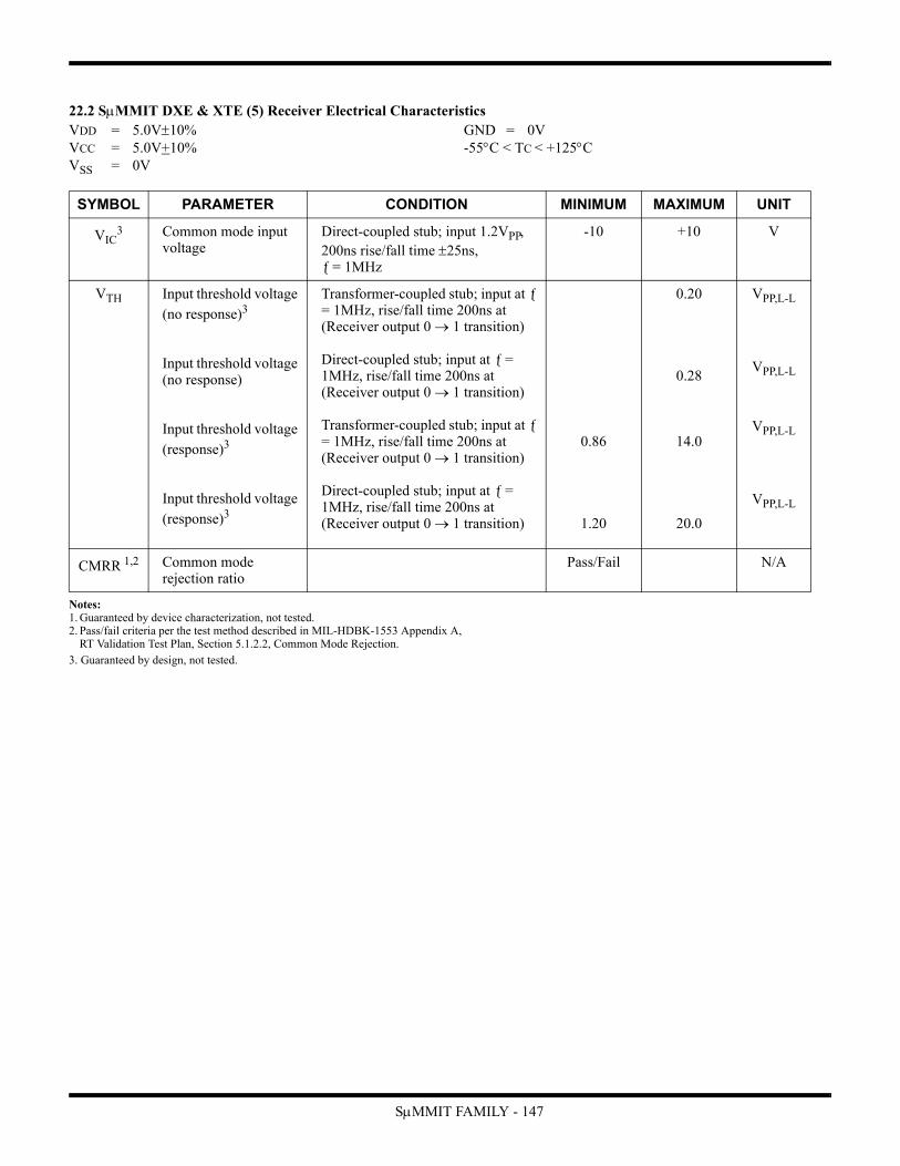
22.2 SMMIT DXE & XTE (5) Receiver Electrical CharacteristicsVDD = 5.0V10%VCC = 5.0V+10%VSS = 0V
GND = 0V-55C < TC < +125C
Notes:1. Guaranteed by device characterization, not tested.2. Pass/fail criteria per the test method described in MIL-HDBK-1553 Appendix A,
RT Validation Test Plan, Section 5.1.2.2, Common Mode Rejection.3. Guaranteed by design, not tested.
SYMBOL PARAMETER CONDITION MINIMUM MAXIMUM UNIT
VIC3 Common mode input
voltageDirect-coupled stub; input 1.2VPP, 200ns rise/fall time 25ns, = 1MHz
-10 +10 V
VTH
Input threshold voltage
(no response)3
Input threshold voltage (no response)
Input threshold voltage
(response)3
Input threshold voltage
(response)3
Transformer-coupled stub; input at = 1MHz, rise/fall time 200ns at (Receiver output 0 1 transition)
Direct-coupled stub; input at = 1MHz, rise/fall time 200ns at (Receiver output 0 1 transition)
Transformer-coupled stub; input at = 1MHz, rise/fall time 200ns at (Receiver output 0 1 transition)
Direct-coupled stub; input at = 1MHz, rise/fall time 200ns at (Receiver output 0 1 transition)
0.86
1.20
0.20
0.28
14.0
20.0
VPP,L-L
VPP,L-L
VPP,L-L
VPP,L-L
CMRR 1,2 Common moderejection ratio
Pass/Fail N/A
SMMIT FAMILY - 147

23.0 SMMIT LXE/DXE & SMMIT XTE TRANSMITTER ELECTRICAL CHARACTERISTICS
23.1 SMMIT LXE & XTE (15 & 12) Transmitter Electrical CharacteristicsVDD = 5.0V10%VCC = 5.0V +10%, -5%VEE = -12.0V or -15.0V5%
VSS = 0V
GND = 0V-55C < TC < +125C
Note:1. Guaranteed by device characterization, not tested.2. Tested in accordance with the method described in MIL-STD-1553B output symmetry, section 4.5.2.1.1.4.3. Guaranteed by design, not tested.
SYMBOL PARAMETER MINIMUM MAXIMUM UNIT CONDITION
VO Output voltage swing
per MIL-STD-1553B 3
(see figure 52)
per MIL-STD-1553B(see figure 52)
per MIL-STD-1553A 3
(see figure 52)
18
6.0
6.0
27
9
20
VPP,L-L
VPP,L-L
VPP,L-L
Transformer-coupled stub, figure 51, Point A; input = 1MHz, RL = 70 ohms
Direct-coupled stub, figure 51, Point A; input = 1MHz, RL = 35 ohms
Figure 51, Point A; input = 1MHz, RL = 35 ohms
VNS 1 Output noise voltage
differential (see figure 52)
14
5
mV-RMS L-L
mV-RMS L-L
Transformer-coupled stub, figure 51, Point A; input = DC to 10MHz, RL = 70 ohms
Direct-coupled stub, figure 51, Point A; input = DC to 10MHz,RL = 35 ohms
VOS 1,2 Output symmetry (see
figure 52)-250
-90
+250
+90
mVPP,L-L
mVPP,L-L
Transformer-coupled stub, figure 51, Point A; RL = 70 ohms, measurement taken 2.5s after end of transmission
Direct-coupled stub, figure 51, Point A; RL = 35 ohms, measurement taken 2.5s after end of transmission
VDIS 1 Output voltage
distortion (overshoot or ring) (see figure 52)
-900
-300
+900
+300
mVpeak,L-L
mVpeak,L-L
Transformer-coupled stub, figure 51, Point A; RL = 70 ohms
Direct-coupled stub, figure 51, Point A; RL = 35 ohms
TIZ 1 Terminal input impedance
1
2
Kohm
Kohm
Transformer-coupled stub, figure 51, Point A; input = 75KHz to 1MHZ (power on or power off; non-transmitting, RL removed from circuit).
Direct-coupled stub, figure 51, Point A; input = 75KHz to 1MHZ (power on or power off; non-transmitting, RL removed from circuit).
SMMIT FAMILY - 148

23.2 SMMIT DXE & XTE (5) Transmitter Electrical CharacteristicsVDD = 5.0V10%VCC = 5.0V +10%VSS = 0V
GND = 0V-55C < TC < +125C
Note:1. Guaranteed by device characterization, not tested.2. Tested in accordance with the method described in MIL-STD-1553B output symmetry, section 4.5.2.1.1.4.
SYMBOL PARAMETER MINIMUM MAXIMUM UNIT CONDITION
VO Output voltage swing
per MIL-STD-1553B 1
(see figure 52)
per MIL-STD-1553B(see figure 52)
per MIL-STD-1553A 1
(see figure 52)
18
6.0
6.0
27
9
20
VPP,L-L
VPP,L-L
VPP,L-L
Transformer-coupled stub, figure 51, Point A; input = 1MHz, RL = 70 ohms
Direct-coupled stub, figure 51, Point A; input = 1MHz, RL = 35 ohms
VNS1 Output noise voltage
differential (see figure 52)
14
5
mV-RMS L-L
mV-RMS L-L
Transformer-coupled stub, figure 51, Point A; input = DC to 10MHz, RL = 70 ohms
Direct-coupled stub, figure 51, Point A; input = DC to 10MHz,RL = 35 ohms
VOS1,2 Output symmetry (see
figure 52)-250
-90
+250
+90
mVPP,L-L
mVPP,L-L
Transformer-coupled stub, figure 51, Point A; RL = 70 ohms, measurement taken 2.5s after end of transmission
Direct-coupled stub, figure 51, Point A; RL = 35 ohms, measurement taken 2.5s after end of transmission
VDIS1 Output voltage
distortion (overshoot or ring) (see figure 52)
-900
-300
+900
+300
mVpeak,L-L
mVpeak,L-L
Transformer-coupled stub, figure 51, Point A; RL = 70 ohms
Direct-coupled stub, figure 51, Point A; RL = 35 ohms
TIZ1 Terminal input
impedance1
2
Kohm
Kohm
Transformer-coupled stub, figure 51, Point A; input = 75KHz to 1MHZ (power on or power off; non-transmitting, RL removed from circuit).
Direct-coupled stub, figure 51, Point A; input = 75KHz to 1MHZ (power on or power off; non-transmitting, RL removed from circuit).
SMMIT FAMILY - 149

24.0 SMMIT LXE/DXE & SMMIT XTE AC ELECTRICAL CHARACTERISTICS
24.1 SMMIT LXE & XTE (15 & 12) AC Electrical CharacteristicsVDD = 5.0V10%VCC = 5.0V +10%, -5%VEE = -12.0V or -15.0V5%
VSS = 0V
GND = 0V-55C < TC < +125C
24.2 SMMIT DXE & XTE (5) AC Electrical CharacteristicsVDD = 5.0V10%VCC = 5.0V +10%VSS = 0V
GND = 0V-55C < TC < +125C
SYMBOL PARAMETER MINIMUM MAXIMUM UNIT CONDITION
tR, tF Transmitter output rise/fall time (see figure 53)
100 300 ns Input = 1MHz 50% duty cycle: direct-coupled RL = 35 ohms output at 10% through 90% points TXOUT, TXOUT. Figure 53.
tRZCD Zero crossing distortion (see figure 54)
-150 150 ns Direct-coupled stub; input = 1MHz, 3 VPP (skew INPUT 150ns), rise/fall time 200ns.
tTZCS Zero crossing stability (see figure 54)
-25 25 ns Input TXIN and TXIN should create Transmitter output zero crossings at 500ns, 1000ns, 1500ns, and 2000ns. These zero crossings should not deviate more than 25ns.
SMMIT FAMILY - 150

Figure 52. Transceiver Test Circuit MIL-STD-1553B
A
TERMINAL
Notes:1. Transformer Coupled Stub:
Terminal is defined as transceiver plus isolation transformer. 2. Direct Coupled Stub:
Terminal is defined as transceiver plus isolation transformer and fault resistors.
RL
TXOUT
TXOUT
SMMIT FAMILY - 151

Figure 53. Transmitter Output Characteristics (VDIS, VOS, VNS, VO)
Figure 54. Transmitter Output Zero Crossing Stability, Rise Time, Fall Time (tTZCS, tR, tF)
Figure 55. Receiver Input Zero Crossing Distortion (tRZCD)
0 Volts 0 Volts
VDIS (Ring) VDIS (Overshoot)
VO VNS VOS
90%
10%10%
90%
VO
tR
tF
tTZCS
Zero crossing stability + 25ns
tRZCD
Zero crossing distortion + 150ns
VIN
SMMIT FAMILY - 152

25.0 PACKAGING
Notes:1. All package finishes are per MIL-PRF-38535.2. Letter designations are for cross-reference to MIL-STD-1835.3. Numbering and lettering on the ceramic are not subject to visual or marking criteria.4. True position applies to pins at the base plane (datum C).5. True position applies at pin tips.6. Pin C3 is a guide pin only.7. Approximately 9.0 grams.
Figure 56. SMMIT E 85-Pin Pingrid Array
e0.100TYP.
L
K
J
H
G
F
E
D
C
B
A
1 2 3 4 5 6 7 8 9 10 11
PIN #1 ID BOTTOM VIEW A-A 0.003 MIN. TYP.
D1/E11.000
0.070 + 0.010 DIA. TYP.
TOP VIEW
STANDOFF0.050 DIA + 0.005
PIN 1 ID
PLATING TAB OPTIONAL
-A-D1.100 + 0.012
0.100
E1.100+ 0.012
0.080 REF. TYP.
0.040 REF. TYP.
VSS VDD
VD
DQ
VS
SQ
VS
SQ
VD
DQ
-B-
SIDE VIEW
A10.1140.080 L
A
A
-C-(BASE PLANE)
Q0.050 + 0.010
b0.018 + 0.002
55-P
GA
7127
VDD VSS
SMMIT FAMILY - 153

Notes:1. All package finishes are per MIL-PRF-38535.2. Letter designations are for cross-reference to MIL-STD-1835.
3. Numbering and lettering on the ceramic are not subject to visual or marking criteria.
4. Approximately 8.0 grams.
Figure 57. SMMIT E 85-Lead Flatpack(50mil lead spacing)
BOTTOM VIEW A-A
TOP VIEW SIDE VIEW
DETAIL A
0.005 MIN. TYP.L0.0260MIN.REF.
0.000 MIN.
C0.007 + 0.001
0.007 + 0.001
A
A0.108 MAX.
A10.088/0.072
SEE DETAIL A
LEAD KOVAR
PLATING TAB OPTIONAL
b0.016 + 0.002
e0.050 TYP.
0.040 REF. TYP.
0.040 REF. TYP.
VDDQVSSQ
VS
SV
DD
VDDQ VSSQ
VS
SV
DD
84-F
P7
023
HD/HE1.810 + 0.015 SQ.D/E1.150 + 0.0120.040 REF. TYP.
PIN 1 I.D.GEOMETRY OPTIONAL(Counter-Clockwise)
A
SMMIT FAMILY - 154

SMMIT FAMILY - 155
Figure 58. SMMIT E 132-Lead Flatpack

-A-D1.310±0.015
INDEX MARKIN THIS AREA
0.070 X 45º REF.0.040 REF.0.040 REF.
0.130 REF.
E1.060±0.015
-B-
A
A
-C-
BASE PLANE
A0.1250.100
0.3150.270
L0.180±0.008
TOP VIEW
Notes:1. True position applies to pins at base plane (datum C).2. True position applies at pin tips.3. All package finishes are per MIL-PRF-38535.4. Letter designations are for cross-reference to MIL-STD-1835.BOTTOM VIEW A-A
SIDE VIEW
0.030 M C A B 1
2 C
0.018±0.002
D11.150
0.100e0.050
0.900
0.600
0.037 MIN.TYP.
DCBA
WVUT
DIE OUTLINES SHOWN FORREFERENCE ONLY
INDEX MARK
VSSQ VDDQ
VSSVDD96pin 7137
1 2 3 4 5 6 7 8 9 10 12 14 16 18 20 22 24
(3 PLACES)
Figure 59. SMMIT LXE/DXE 96-Pin Pingrid Array
M
MM
SMMIT FAMILY - 156

Figure 60. SMMIT LXE/DXE 100-Lead
SMMIT FAMILY - 157

SMMIT FAMILY - 158
Figure 61. SMMIT XTE139-pin PGA
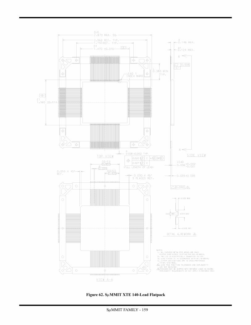
SMMIT FAMILY - 159
Figure 62. SMMIT XTE 140-Lead Flatpack
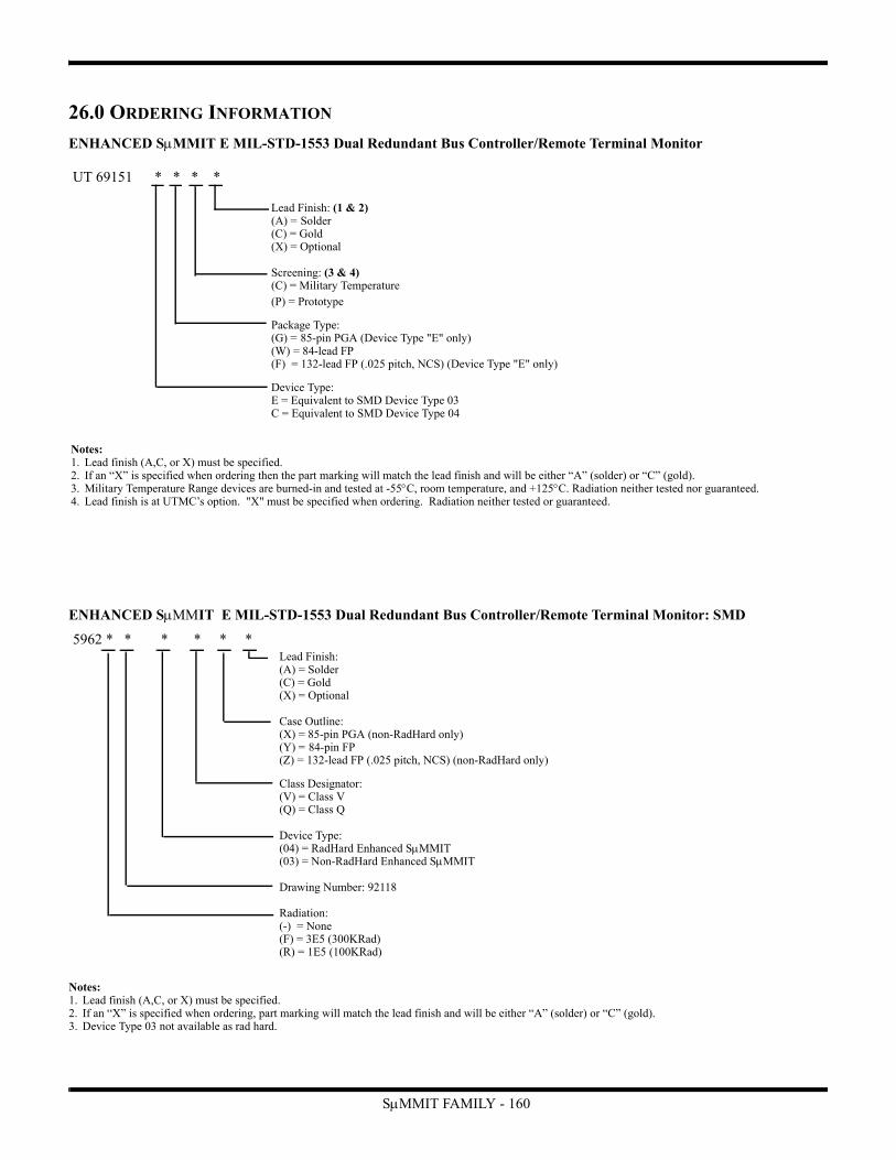
SMMIT FAMILY - 160
26.0 ORDERING INFORMATION
ENHANCED SMMIT E MIL-STD-1553 Dual Redundant Bus Controller/Remote Terminal Monitor
UT 69151 * * * *
Lead Finish: (1 & 2)(A) = Solder (C) = Gold(X) = Optional
Screening: (3 & 4)(C) = Military Temperature (P) = Prototype
Package Type:(G) = 85-pin PGA (Device Type "E" only)(W) = 84-lead FP(F) = 132-lead FP (.025 pitch, NCS) (Device Type "E" only)
Device Type:E = Equivalent to SMD Device Type 03 C = Equivalent to SMD Device Type 04
Notes:1. Lead finish (A,C, or X) must be specified.2. If an “X” is specified when ordering then the part marking will match the lead finish and will be either “A” (solder) or “C” (gold).3. Military Temperature Range devices are burned-in and tested at -55C, room temperature, and +125C. Radiation neither tested nor guaranteed.4. Lead finish is at UTMC’s option. "X" must be specified when ordering. Radiation neither tested or guaranteed.
ENHANCED SIT E MIL-STD-1553 Dual Redundant Bus Controller/Remote Terminal Monitor: SMD
5962 * * * * * *Lead Finish:(A) = Solder (C) = Gold(X) = Optional
Case Outline:(X) = 85-pin PGA (non-RadHard only)(Y) = 84-pin FP(Z) = 132-lead FP (.025 pitch, NCS) (non-RadHard only)
Class Designator:(V) = Class V(Q) = Class Q
Device Type: (04) = RadHard Enhanced SMMIT(03) = Non-RadHard Enhanced SMMIT
Drawing Number: 92118
Radiation:(-) = None(F) = 3E5 (300KRad)(R) = 1E5 (100KRad)
Notes:1. Lead finish (A,C, or X) must be specified.2. If an “X” is specified when ordering, part marking will match the lead finish and will be either “A” (solder) or “C” (gold).3. Device Type 03 not available as rad hard.
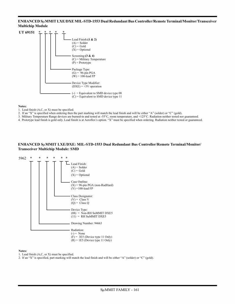
SMMIT FAMILY - 161
ENHANCED SMMIT LXE/DXE MIL-STD-1553 Dual Redundant Bus Controller/Remote Terminal/Monitor/Transceiver Multichip Module
Lead Finish:(1 & 2)(A) = Solder (C) = Gold(X) = Optional
Screening:(3 & 4)(C) = Military Temperature(P) = Prototype
Package Type:(G) = 96-pin PGA(W) = 100-lead FP
Device Type Modifier:(DXE) = +5V operation
(-) = Equivalent to SMD device type 08 (C) = Equivalent to SMD device type 11
Notes:1. Lead finish (A,C, or X) must be specified.2. If an “X” is specified when ordering then the part marking will match the lead finish and will be either “A” (solder) or “C” (gold).3. Military Temperature Range devices are burned-in and tested at -55C, room temperature, and +125C. Radiation neither tested nor guaranteed.4. Prototype lead finish is gold only. Lead finish is at Aeroflex’s option. “X” must be specified when ordering. Radiation neither tested or guaranteed.
ENHANCED SMMIT LXE/DXE: MIL-STD-1553 Dual Redundant Bus Controller/Remote Terminal/Monitor/Transceiver Multichip Module: SMD
5962 * * * * * *
Notes:1. Lead finish (A,C, or X) must be specified.2. If an “X” is specified, part marking will match the lead finish and will be either “A” (solder) or “C” (gold).
Lead Finish:(A) = Solder (C) = Gold(X) = Optional
Case Outline:(X) = 96-pin PGA (non-RadHard)(Y) =100-lead FP
Class Designator: (V) = Class V(Q) = Class Q
Device Type:(08) = Non-RH SuMMIT DXE5(11) = RH SuMMIT DXE5
Drawing Number: 94663
Radiation:(-) = None(F) = 3E5 (Device type 11 Only)(R) = 1E5 (Device type 11 Only)
UT 69151 * * * * *

SMMIT FAMILY - 162
ENHANCED SMMIT XTE MIL-STD-1553 Dual Redundant Bus Controller/Remote Terminal/Monitor/Transceiver Multichip Module
Radiation:None
Lead Finish: (1 & 2)(A) = Solder (C) = Gold(X) = Optional
Screening: (3 & 4)(C) = Military Temperature(P) = Prototype
Package Type:(Z) = 139-pin PGA(W) = 140-pin FP
Device Type Modifier:(XTE5) = +5V operation
Notes:1. Lead finish (A,C, or X) must be specified.2. If an “X” is specified when ordering then the part marking will match the lead finish and will be either “A” (solder) or “C” (gold).3. Military Temperature Range devices are burned-in and tested at -55C, room temperature, and +125C. Radiation neither tested nor guaranteed.4. Prototype asembly are tested at +25C only. Lead finish is GOLD only. Radiation neither tested or guaranteed.
ENHANCED SMMIT XTE: MIL-STD-1553 Dual Redundant Bus Controller/Remote Terminal/Monitor/Transceiver Multichip Module: SMD
5962 * * * * * *
Notes:1. Lead finish (A,C, or X) must be specified.2. If an “X” is specified, part marking will match the lead finish and will be either “A” (solder) or “C” (gold).
Lead Finish:(A) = Solder (C) = Gold(X) = Optional
Case Outline:(Y) = 140-pin FP(Z) = 139-pin PGA
Class Designator: (Q) = Class Q
Device Type:(08) = SuMMIT XTE 5V/5V
Drawing Number: 94758
Radiation:None
UT 69151 - * * * * *