Embed Size (px)
Citation preview

254 IEEE TRANSACTIONS ON VERY LARGE SCALE INTEGRATION (VLSI) SYSTEMS, VOL. 11, NO. 2, APRIL 2003
Energy-Efficiency Bounds for Deep Submicron VLSISystems in the Presence of Noise
Lei Wang, Member, IEEE,and Naresh R. Shanbhag, Senior Member, IEEE
Abstract—In this paper, we present an algorithm for computingthe bounds on energy-efficiency of digital very large scale inte-gration (VLSI) systems in the presence of deep submicron noise.The proposed algorithm is based on asoft-decision channelmodelof noisy VLSI systems and employs information–theoretic argu-ments. Bounds on energy-efficiency are computed for multimodulesystems, static gates, dynamic circuits and noise-tolerant dynamiccircuits in 0.25- m CMOS technology. As the complexity of theproposed algorithm grows linearly with the size of the system, itis suitable for computing the bounds on energy-efficiency for com-plex VLSI systems. A key result presented is that noise-tolerantdynamic circuits offer the best trade off between energy-efficiencyand noise-immunity when compared to static and domino circuits.Furthermore, employing a 16-bit noise-tolerant Manchester adderin a CDMA receiver, we demonstrate a 31.2%–51.4% energy re-duction over conventional systems when operating in the presenceof noise. In addition, we compute the lower bounds on energy dis-sipation for this CDMA receiver and show that these lower boundsare 2.8 below the actual energy consumed, and that noise-toler-ance reduces the gap between the lower bounds and actual energydissipation by a factor of 1.9 .
Index Terms—CDMA communications, deep submicron noise,energy-efficiency bounds, low power, noise-tolerance.
I. INTRODUCTION
T HE ABILITY to scale CMOS technology [1]–[3] has beena key driver for the development of low-cost broadband
communication and computing systems. However, with featuresizes being scaled into the deep submicron (DSM) regime,DSM noise [4], [5] consisting of ground bounce, crosstalk,
drops, clock jitter, charge sharing, process variations, etc.,has emerged as a critical factor that may ultimately determinethe performance achievable in the future at an affordable cost.Compounding the problem further is the adoption of aggressivedesign practices such as dynamic logic, low-supply voltage, useof low- and hence, high-leakage devices, and high clock-fre-quencies. As a result, the semiconductor industry is facing areliability problem that challenges the very foundation of thecost and performance benefits of very large scale integration(VLSI).
In this paper, we address the issue of determining achiev-able bounds on energy-efficiency for digital VLSI systems in
Manuscript received August 14, 2001; revised February 8, 2002. This workwas supported by the National Science Foundation under Grant CCR-0000987and Grant CCR-9979381.
L. Wang is with Microprocessor Technology Laboratories, Hewlett-PackardCompany, Fort Collins, CO 80521 USA (e-mail: [email protected]).
N. R. Shanbhag is with the Coordinated Science Laboratory, Department ofElectrical and Computer Engineering, University of Illinois at Urbana-Cham-paign, Urbana, IL 61801 USA (e-mail: [email protected]).
Digital Object Identifier 10.1109/TVLSI.2003.810783
the presence of noise. The issue of lower bounds on power dis-sipation was addressed in [6] by considering thermal noise asthe limiting factor for energy reduction. In [7], the lower boundson power dissipation per pole for analog circuits and empiricallower bounds for digital circuits were derived from the desiredsignal-to-noise ratio (SNR) by assuming noise-free elements.
In the past, we have proposed aninformation-theoretic frame-work [8] that enables us to determine the bounds on energy-ef-ficiency in a rigorous manner. The central thesis of this frame-work is to establish an energy-related correspondence betweenan algorithm and its architectural implementation. Specifically,we view a DSM VLSI system as a network of communicationchannels; a view also echoed recently in the ITRS2001 [1]. Thealgorithmic complexity of the system is quantified by thein-formation transfer rate , while each implementation is said tohave aninformation transfer capacity . Employing the infor-mation-theoretic constraint on reliability [9], we pre-sented [8] a common basis for various power reduction tech-niques such as voltage scaling, pipelining, parallel processing,adiabatic logic, etc. The same constraint was utilized in [10] toobtain the fundamental limit on signal energy transfer during abinary switching transition. In [11], we proposed abinary sym-metric channel(BSC) model to determine the lower bounds onenergy dissipation for single-output static modules. An infor-mation-theoretic approach was also employed in [12] to deter-mine the maximum achievable energy-reduction in high-speedbusses.
While the proposed information-theoretic approach enablesthe computation of energy-efficiency bounds, it does not di-rectly enable the construction of low-power design techniques.Fortunately, the proposed approach does indicate that designtechniques based onnoise-tolerance, in contrast tonoise mit-igation, can enable the design of systems that operate at orclose to their energy-efficiency bounds. Indeed, our past work[13]–[16] has shown that design techniques based on noise-tol-erance at the algorithmic level [or algorithmic noise-tolerance(ANT)] [13], [14] and at the circuit level [15], [16] are effec-tive in achieving energy-efficiency in the presence of noise. Inthe long run, we see algorithmic and circuit level noise-toler-ance techniques being applied concurrently to design systemswith energy consumption that approach these bounds. Indeed,error-tolerancehas been referred to as one of the difficult de-sign challenges in the next decade [1].
Ideally, we would like to be able to compute energy-efficiencybounds for complex systems and then employ a combinationof algorithmic and circuit level noise-tolerance techniques toapproach these bounds. Unfortunately, computing the boundsfor complex systems is quite difficult at present. Thus, we are
1063-8210/03$17.00 © 2003 IEEE

WANG AND SHANBHAG: ENERGY-EFFICIENCY BOUNDS FOR DEEP SUBMICRON VLSI SYSTEMS 255
faced with a “gap” between our ability to compute bounds onenergy-efficiency for a specific system and our ability to devisedesign techniques for approaching these bounds. Fortunately,thesoft-decision channel(SDC) model presented in this paperholds the promise that lower bounds on energy-efficiency can becomputed for complex systems. An evidence of this promise ispresented in this paper where we compute the bounds on energy-efficiency for multi-input multi-output systems and for a CDMAreceiver. Specific examples where the above mentioned gap isbridged are the chip I/O signaling [11] and the CDMA receiverexample in this paper.
Employing the proposed SDC model, we obtain the lowerbounds on energy-efficiency for static, domino [19], and noise-tolerant domino [15] gates. We show that noise-tolerant gateshave a lower bound that is smaller than the corresponding boundfor a domino gate when operating in the presence of noise. Thisis an interesting result because noise-tolerance implies an en-ergy overhead and thus it is not obvious that it is an energy-effi-cient design technique. Note that while the proposed SDC modelenables us to compute the lower bounds on energy-efficiency, itdoes not indicate the design technique to employ. Nevertheless,this paper presents simple examples that do suggest that designtechniques based on noise-tolerance can be quite effective inachieving energy-efficiency in the presence of noise.
In Section II, we briefly review our past work on the in-formation-theoretic framework. In Section III, we propose thesoft-decision channel model for noisy VLSI systems and de-velop the associated information-theoretic measures. In Sec-tion IV, we determine the lower bounds on energy-efficiency bysolving an energy optimization problem. In Section V, we em-ploy noise-tolerance to design an adder circuit that approachesthe lower bounds on energy-efficiency in the presence of noise.
II. I NFORMATION-THEORETICFRAMEWORK: A REVIEW
In this section, we review our past work on the information-theoretic framework for deriving the lower bounds on energydissipation of noisy logic gates.
From Shannon’s joint source-channel coding theory [9], theinformation content of a continuous sourceis given by
(1)
where is the probability density function (PDF) of a con-tinuous-valued output .
Assume that the output of the sourceis passed through anoisy transformation , i.e.,
(2)
where is a deterministic mapping function from to, and denotes the noise, which is typically assumed to
be white with a Gaussian distribution but could also have an ar-bitrary distribution. The maximum information content that thenoisy transformation can transfer with arbitrarily low proba-bility of error is given by its capacity as
(3)
(a)
(b)
Fig. 1. A simple information transfer system. (a) A 2-inputOR gate. (b) Thecorresponding BSC model.
where is the information transfer capacity per use,is therate at which the system is being operated, and is themutual information, which is defined as
(4)
and is the conditional entropy of conditioned on .In [8], we have shown that any transformationwith input
and output has an information transfer rategiven by, where is the entropy of the output and is
the rate at which the original input data are being generated by asource. Note that can be different from due to input coding.Information theory [9] indicates that it is possible to achieve aninformation transfer rate with arbitrarily low probability oferror (by properly coding the input) as long as .
The lower bounds on energy dissipation for single-outputstatic gates have been studied previously [11] by modelingnoisy gates as a binary symmetric communication channel(BSC) and employing information-theoretic concepts. Considera 2-inputOR gate as shown in Fig. 1(a), where the inputisgenerated from . Due to noise, the outputof the gate will deviate from its nominal values. Assume thatthe output is passed through a hard-decision device such as alatch. The latched output, denoted by, can be regarded as abinary signal that contains errors with a probability. This canbe represented by the BSC model as shown in Fig. 1(b).
Employing the BSC model, the lower bounds on energy dissi-pation of single-output static gates can be determined under theinformation-theoretic constraint . A key advantage ofthe BSC model is that it can be used to model logic errors quiteeasily. However, the BSC model has two disadvantages. First,the complexity of a BSC model for a complex VLSI system isvery high. Second, the energy-efficiency bounds obtained usingthe BSC model will not be as accurate as those obtained frommodels that do not quantize the output and noise. In this paper,we propose a model that eliminates these drawbacks.
III. T HE SDC MODEL
In this section, we develop a SDC model for DSM VLSI sys-tems. We first provide a physical basis for the proposed modeland then develop the channel capacity formula to compute thebounds on energy-efficiency.

256 IEEE TRANSACTIONS ON VERY LARGE SCALE INTEGRATION (VLSI) SYSTEMS, VOL. 11, NO. 2, APRIL 2003
(a)
(b)
Fig. 2. The proposed SDC model for noisy gates. (a) Voltage waveforms and(b) output distribution.
A. SDC Model
The proposed SDC model for a single-output noisy gate is il-lustrated in Fig. 2(a). In the presence of noise, the voltage wave-form at the output is composed of an ideal output voltageand additive noise voltage that is assumed to be independentof the input and output , i.e.,
(5)
The ideal output is a binary signal with a statistical distri-bution given by and ,where is determined by the input statistics and the logic func-tion of the gate. The noise voltagerepresents a composite ef-fect due to thermal noise and other DSM phenomena such asground bounce, crosstalk, charge-sharing, leakage, and processvariations. In this paper, we assume that the noise voltagehasa PDF denoted by . From (5), the statistical distribution
of the noisy output can be expressed as
if
if .(6)
Note that can be considered as a bimodal continuousrandom signal whose value is either or . A typicaldistribution of is depicted in Fig. 2(b), from which we canrewrite as
(7)
It can be shown that the previously proposed BSC model [11]is a special case of the proposed SDC model when the inputand output of a noisy gate are latched synchronously. Assumethat the latch being employed has a logic threshold denoted by
. Thus, noise voltage can introduce logic errors atthe output of the latch with a probabilitygiven by
(8)There are two fundamental differences between the BSC modeland the proposed SDC model. First, the BSC model quantizesnoise contributions by employing error probabilityin the com-putation of lower bounds. This requires noiseless hard-decisiondevices (e.g., latches) employed at the inputs and outputs ofnoisy gates. The proposed SDC model relaxes this constraint bymodeling noiseless logic signals as binary signals with voltagelevels and 0 V and signaling probability , and DSM noiseas a continuous random signal with a specific statistical distri-bution. Thus, all the signals and noise are captured in such a waythat reflects their inherent physical nature.
Second, the proposed SDC model leads to an efficient algo-rithm to compute the lower bounds on energy dissipation. Thecomputational complexity of the algorithm increases linearlywith system complexity, making the SDC model applicable tocomplex digital systems. We will discuss this point in detail inSection IV.
B. Information Transfer Capacity
We now derive the information transfer capacity for DSMVLSI systems using the proposed SDC model. We start witha simple -input, single-output logic gate and then extend theframework to complex systems. Lemma 1 presented below pro-vides the formula of mutual information for noisy gates. It isthen employed in deriving the information transfer capacity inTheorem 1.
Lemma 1: Consider a noisy digital gate withbinary inputsand single output , where
is the noiseless output and all the noise sources contributea noise voltage with a distribution denoted by . Themutual information for this gate isgiven by
(9)
where is the PDF of , given by
(10)
The proof of Lemma 1 is straightforward. From the definitionof mutual information (4), we have
(11)
where both and are continuous signals. Substitutingand into (11) and using (1), we get (9).
Note that given by (9) is a func-tion of supply voltage , noise distribution , and output

WANG AND SHANBHAG: ENERGY-EFFICIENCY BOUNDS FOR DEEP SUBMICRON VLSI SYSTEMS 257
(a)
(b)
Fig. 3. Mutual information with respect toV andp . (a)� = 0:4 V. (b) The increase for� = 0:3 V.
probability . The value of is determined by the input sta-tistics and the logic function of the gate. In general, it is difficultto obtain an analytical solution for (9); however, numerical so-lutions are easy to obtain [20].
From Lemma 1, we obtain the information transfer capacityper use as summarized below.
Theorem 1: The information transfer capacity per use ofan -input, single-output noisy gate is given by
(12)
The proof of Theorem 1 is provided in Appendix A. Theorem1 indicates that the capacity per use is achieved when the
ideal output has a uniform distribution [i.e.,]. This is consistent with the observation that
implies maximum uncertainty in and hence, thelargest information content being transferred.
Fig. 3(a) plots the mutual information usingLemma 1 for a 2-inputOR gate in a 0.25 m CMOS process.The noise voltage is assumed to be a zero-mean Gaussiandistribution with a variance V. As indicated, forevery supply voltage , reaches the maximumwhen . In addition, is symmetric around
. This is consistent with the BSC model. The capacityper use approaches 1 b/use as increases. This can beinterpreted as the ability of the 2-inputOR gate to transfer 1bit of information for every use provided the supply voltage
258 IEEE TRANSACTIONS ON VERY LARGE SCALE INTEGRATION (VLSI) SYSTEMS, VOL. 11, NO. 2, APRIL 2003
is sufficiently high with respect to noise. This is to beexpected given the fact that for high enough, noise becomesnegligible and the gate can be approximated as being noiseless.On the other hand, decreases toward zero with the reductionin . This reflects the practical scenario where the gate stopsfunctioning on being powered down.
The impact of noise on is illustrated in Fig. 3(b), wherewe observe an increase in (and hence ) as noisevariance being reduced from 0.4 V to 0.3 V. Obviously, agate operating in a less noisy medium is more robust and hencecan transfer more information.
We now compute the information transfer capacity. Assumethat the NMOS and PMOS transistors being used are balancedimplying the same low-to-high and high-to-low delays. Themaximum signaling rate at a supply voltage can beapproximated by [21]
(13)
where is the transconductance of the balanced NMOS andPMOS transistors, is the load capacitance, is the transistorthreshold voltage, and is the velocity saturation index rangingfrom 1 (velocity saturated) to 2 (without velocity saturation).The information transfer capacity can be obtained as ,where and are given by (12) and (13), respectively.
As an example, we consider the 2-inputOR gate in a 0.25m CMOS process with the following parameters: 1)
A/V , 2) V, 3) fF, 4) ,and 5) information transfer rate MB/s. The noisevoltage is assumed to be a zero-mean Gaussian distributionwith a variance V. With V, we obtain
b/use and GHz. Therefore, the informationtransfer capacity of the gate is given byGb/s. Similarly, with V, we obtain b/useand Ghz. This gives MB/s, which is stilllarger than the information transfer requirement, implyingthat through appropriate coding, the gate can be operated re-liably at a supply voltage as low as 1.0 V. The degradation in
is primarily due to noise impact becoming increasingly sig-nificant as reduces. Present-day digital circuits operate atsufficiently high voltages so that b/use and hencecan be as high as .
It is worth mentioning that (12) and (13) provide a direct cor-respondence between the information transfer capacityandimplementation details such as supply voltage, load capacitance,circuit style, CMOS process, and noise parameters. While inthis paper we employ rather general models for speed and noise,any specific assumptions or modifications can be easily incor-porated into the framework. One such example is the computa-tion of bounds on energy dissipation for noise-tolerant circuittechniques (see Section IV-D), where noise contributions aremodeled as an input noise voltage rather than at the output as inthe SDC model. Assuming the gate with a voltage transfer char-acteristic (VTC) function [22], the equivalent output noisevoltage can be expressed as
(14)
Fig. 4. The SDC model for noisy digital systems.
and has a distribution given by [23]
(15)
where and are the PDFs for the input noisevoltage and the equivalent output noise voltage , re-spectively, and is the root of (14). Thus, we can compute theinformation transfer capacity for gates subject to input noise bysubstituting into (9), (10), and (12).
IV. L OWER BOUNDS ONENERGY DISSIPATION
In this section, we determine the lower bounds on energy dis-sipation using the proposed SDC model. These bounds are ob-tained by solving an energy optimization problem while beingsubject to the information-theoretic constraint on re-liability. In Section IV-A, we formulate the constrained opti-mization problem and develop an analytical solution by em-ploying theLagrange multipliermethod [24]. In Section IV-B,we present an algorithm to compute the lower bounds and thenapply it to multimodule systems, dynamic circuits and noise-tol-erant dynamic circuits in Section IV-C to IV-D, respectively.
A. Problem Formulation and Solution
Consider a generic digital system as depicted in Fig. 4. Weassume, without loss of generality, that the system consists of
noisy modules, each generating an ideal (noiseless) outputdenoted by for . The input of the systemis given by , where is a binarysignal. From the SDC model, the total noise contribution can berepresented by output noise voltages .In addition, we assume these noise voltages are independent ofeach other. The outputs of the system can be expressed as
(16)
where denotes the actual voltage waveform at theth outputand is the corresponding noise voltage with a distributiongiven by . Note that the assumption on independent noisesources is pessimistic, i.e., the resulting bounds would be greater

WANG AND SHANBHAG: ENERGY-EFFICIENCY BOUNDS FOR DEEP SUBMICRON VLSI SYSTEMS 259
than those obtained if the noise sources were correlated. This isdue to the fact that independent noise sources incur the largestinformation loss [9] and thus require higher output probabilities
s and transition probabilitiess to compensate. Furthermore,making the independence assumption simplifies the mathemat-ical development so that the key ideas in the paper can be illus-trated clearly.
We consider a silicon implementation where all the NMOSand PMOS transistors share a common power supply andground. In addition, the NMOS and PMOS transistors areproperly sized so that the modules can be operated at the samespeed at a nominal supply voltage. For the sake of simplicity,we assume that all the capacitances including the parasiticcapacitance, interconnect capacitance, and input capacitancefrom the following stage are lumped into the load capacitanceat the output of the system.
In what follows, we consider the total power dissipationto consist primarily of the capacitive component of power dis-sipation, also referred to as dynamic power dissipation ,which is given by [22]
(17)
where and are the average transition probability and theequivalent load capacitance, respectively, for theth output, and
is given by (13). In Section IV-D, we will include other powercomponents (e.g., short-circuit and static power) to determinethe lower bounds for domino and noise-tolerant circuits.
We note that for dynamic circuits such as conventionaldomino, will be equal to the probability of output being
(or a logic “1”), i.e., . This is valid for static circuitsas well provided transition signaling [11] (i.e., a logic “1” isrepresented with a transition and a logic “0” is representedwith no transition) is employed at the output. Therefore, in therest of the paper we will replace in the information capacityexpressions (9)–(12) with the transition probabilityas thesetwo measures are equivalent.
We now determine the lower bounds on energy dissipationfor DSM VLSI systems as shown in Fig. 4, using the SDCmodel. As discussed in Section III, the mutual information
for such systems isdetermined by the supply voltage , output transition prob-abilities and noise parameters. To simplifynotation, we rewrite asan explicit function of these parameters as follows
(18)
where is the variance (energy) of noise voltage, whichis determined by the distribution function . Employingsimilar arguments as in [11], the lower bounds on energy dis-sipation can be obtained by solving the following optimizationproblem
minimize: (19)
subject to:
(20)
where is the energy per information bit.Note that for any given supply voltage and noise
parameters, the information-theoretic constraint (20) andpower dissipation are functions of transition probabilities
. Hence, the optimum solution to (19) and(20) is a set of s ( ) that minimizes thepower dissipation while satisfying the information-theoreticconstraint on reliability. Employing the Lagrange multipliermethod [24], we obtain the optimum solution to (19) and (20)as summarized in Theorem 2.
Theorem 2: The lower bound on energy dissipation for a dig-ital system consisting of noisy modules is achieved with tran-sition probabilities satisfying
(21)
where , , and are the load capacitance, transition prob-ability, and noise variance, respectively, at theth output,is a constant determined by the information-theoretic constrainton reliability, and is the mutual informa-tion for the th output, which is given by
(22)
where is the distribution function for the output noise.The proof of Theorem 2 is provided in Appendix B. In Sec-
tion IV-B to IV-D, we will demonstrate the use of Theorem 2to compute the lower bounds on energy dissipation for variousdigital systems.
B. Computation of Lower Bounds
We assume that the NMOS and PMOS transistors beingused are properly sized to operate at the same speed ata nominal supply voltage. Thus, the parameters and
s are fixed making the lower bounds a function of thesupply voltage and transition probabilities s. FromTheorem 2, the objective is to find an optimum combination
at each such that the powerdissipation is minimized subject to the information-theoreticrequirement . Fig. 5 shows the algorithm for computing thelower bounds. For each we start with a sufficiently small
and compute the values ofs using (21) and (22). Theses are then employed to compute the information transfer
metric andthe result is compared to the information transfer rate. If
, , thevalue of will be increased in small steps until (20) is just

260 IEEE TRANSACTIONS ON VERY LARGE SCALE INTEGRATION (VLSI) SYSTEMS, VOL. 11, NO. 2, APRIL 2003
Fig. 5. The algorithm to compute the lower bounds on energy dissipation.
satisfied. The corresponding transition probabilitiess arethen employed with to obtain the lower bounds. Note thatthe value of in Fig. 5 is determined by the precision towhich the bounds need to be computed. A smaller value ofresults in higher precision. Therefore, one can start with a fixedstep-size and then reduce it as the solution converges.
Note that the proposed algorithm determines the lowerbounds by joint optimization of power components from allthe modules in the system. The associated computationalcomplexity increases linearly with the number of modulesin the system, making the proposed algorithm suitable fordetermining the energy-efficiency bounds of complex digitalsystems. In addition, it can be shown that the lower boundsderived via the SDC model are smaller than those obtained viathe BSC model.
In Section IV-C and IV-D, we will demonstrate the computa-tion of the lower bounds via the proposed SDC model for mul-timodule systems, dynamic circuits, and noise-tolerant circuittechniques.
C. Lower Bounds for Multimodule Systems
We now determine the lower bounds on energy dissipationfor digital systems consisting of multiple logic modules, eachof which generates a noisy output while consuming a certainamount of power. For the purpose of demonstration, we willconsider a full-adder which has a SUM module and a CARRYmodule. The lower bounds for more complex digital systemscan be determined in a similar manner.
We assume the following design parameters for the full-adder.1) The gate is implemented in a 0.25m CMOS process in
static CMOS logic style with dual NMOS and PMOS networks.2) The NMOS and PMOS transistors are balanced with the
same propagation delay. The speed of the gate is given by (13),where fF–30 fF, A/V ,V, and .
3) The noise voltage has a zero-mean Gaussian distributionwith V–0.4 V. The noise is uncorrelated to the desiredinput and output signals.
4) The gate has an information transfer rate requirementMb/s.
Note that in practice the CARRY and SUM modules are pos-sibly subject to noise with different amplitudes or driving dif-ferent load capacitances. This results in different energy boundsand, hence, we will evaluate them separately.
We first consider the case where the two modules are sub-ject to different noise amplitudes but with the same load capac-itance of 30 fF. We assume that the noise voltages and
are zero-mean Gaussian distributions withV and V, respectively. This implies a more reliableCARRY module. Fig. 6(a) illustrates the lower bounds for theSUM module, CARRY module and the full-adder. Note that thelower bound for the full-adder is obtained by jointly optimizingthe power components of different modules under the informa-tion-theoretic constraint on reliability. The minimum values ofenergy per information bit for the SUM module, CARRYmodule and the full-adder equal 5.1 fj/b, 6.7 fJ/b and 12 fJ/bat V, 1.0 V and 1.08 V, respectively. Also shown in

WANG AND SHANBHAG: ENERGY-EFFICIENCY BOUNDS FOR DEEP SUBMICRON VLSI SYSTEMS 261
(a)
(b)
Fig. 6. Lower bounds on energy dissipation for multimodule systems subject to (a) different noise and (b) different load capacitances.
Fig. 6(a) is that the lower bound for the full-adder is achievedwhen the CARRY module consumes more energy than the SUMmodule does.
Fig. 6(b) illustrates the lower bounds on energy dissipationwhen the SUM and CARRY modules drive different load ca-pacitances of 20 fF and 30 fF, respectively, but subject to thesame noise amplitude ( V). It indicates that the lowerbound for the full-adder is achieved when the output driving alarger capacitance consumes less energy. This is to be expected
because such output will have a smaller transition probability[see (21)] which offsets the energy overhead due to the large ca-pacitance.
D. Energy-Efficiency Bounds for Noise-Tolerant Circuits
Noise-tolerant circuit techniques [15]–[18] improvenoise-immunity by employing additional elements to preventlogic errors from occurring in the presence of noise. Thus, onewould expect noise-tolerant circuits to be less energy-efficient

262 IEEE TRANSACTIONS ON VERY LARGE SCALE INTEGRATION (VLSI) SYSTEMS, VOL. 11, NO. 2, APRIL 2003
(a)
(b)
Fig. 7. Dynamic style 3-inputOR gates. (a) Conventional domino. (b) Mirrortechnique.
than conventional circuits. In this subsection, we determine thelower bounds on energy-efficiency for noise-tolerant circuittechniques such as the mirror technique [15]. It will be shownthat noise-tolerance improves the energy-efficiency whenoperating at the lower bound.
Fig. 7 depicts two 3-inputOR gates implemented by the con-ventional domino (with a keeper) and the mirror technique ina 0.25 m CMOS technology. It is known that domino circuitsare inherently susceptible to noise [5] due to their low switchingthreshold voltage , defined as the input voltage at which theoutput changes state. For the dominoORgate shown in Fig. 7(a),
, where is the threshold voltage of an NMOS tran-sistor. The previously proposed mirror technique [15] improvesnoise-immunity via employing two identical NMOS evaluationnets. One additional NMOS transistor M1, whose gate voltage iscontrolled by the dynamic node voltage, provides a conductionpath between the common nodeof the two evaluation nets and
- . During the precharge phase, transistor M1 is turned on
and the common node voltage is charged up to ( - – ).Due to body-effect, the switching threshold voltage of the upperNMOS net is increased, thereby improving the noise-immunity.Note that the noise-immunity of the gate can be tuned by eitherchanging the voltage - or resizing the transistor M1.
The total power dissipation of digital gates consists ofdynamic power , short-circuit power and static power
, where has two components (due to sub-threshold leakage) and (due to DC power dissipation).Considering the fact that the two gates in Fig. 7 haveand is relatively small (this is because V), weexpress the total power dissipation as
(23)
where is the average short-circuit current evaluated over eachsignaling period when the gate switches. Note that the two gatesconsume nontrivial short-circuit power as indicated in Fig. 7.
From (23), the problem of deriving the energy-efficiencybounds for domino and mirror circuits is stated as follows:
minimize:
subject to: (24)
From Theorem 2, the solution to (24) can be obtained as
(25)where is the signaling period.
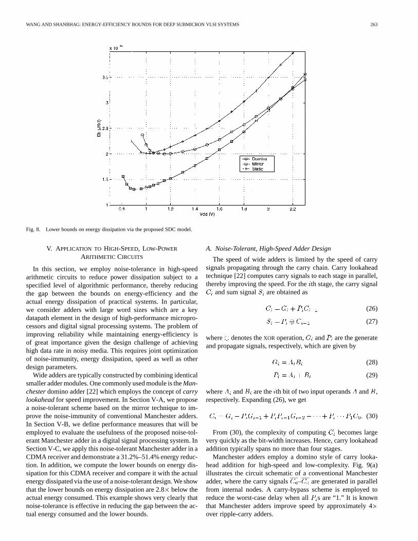
Fig. 8 illustrates the lower bounds derived from the proposedSDC model for a 3-input static, domino, and mirrorOR gates.The mirror gate was designed to have - with M1being eight times the minimum size. For consistency, we sizedthe transistors in all three gates to operate at the same speed atnominal V while driving a 30 fF load. This impliesthat the pull-down NMOS transistors in Fig. 7(b) are sized upresulting in larger parasitic capacitances. We account for thisdesign overhead by extracting the capacitances from the layoutand adding them to the 30 fF load capacitance. Please note thatduring the computation of the lower bounds we relax the speedconstraint and instead keep only the constraint on the informa-tion transfer rate Mb/s. We assume all three gatesto be subject to an input noise voltage which is zero-meanGaussian with V. The equivalent output noise volt-ages are obtained from (14) and (15). As shown, the minimum
of the conventional domino gate is found to be 20 fJ/b,whereas that of the mirror gate is 13 fJ/b, which is 35% lower.Furthermore, we also see that the static gate, while being inher-ently noise-tolerant, is also energy-inefficient when operating atthe lower bound.
Thus, we find that from an information-theoretic perspec-tive, noise-tolerant circuits provide the best trade off betweennoise-immunity and energy-efficiency than either domino orstatic circuits.
WANG AND SHANBHAG: ENERGY-EFFICIENCY BOUNDS FOR DEEP SUBMICRON VLSI SYSTEMS 263
Fig. 8. Lower bounds on energy dissipation via the proposed SDC model.
V. APPLICATION TO HIGH-SPEED, LOW-POWER
ARITHMETIC CIRCUITS
In this section, we employ noise-tolerance in high-speedarithmetic circuits to reduce power dissipation subject to aspecified level of algorithmic performance, thereby reducingthe gap between the bounds on energy-efficiency and theactual energy dissipation of practical systems. In particular,we consider adders with large word sizes which are a keydatapath element in the design of high-performance micropro-cessors and digital signal processing systems. The problem ofimproving reliability while maintaining energy-efficiency isof great importance given the design challenge of achievinghigh data rate in noisy media. This requires joint optimizationof noise-immunity, energy dissipation, speed as well as otherdesign parameters.
Wide adders are typically constructed by combining identicalsmaller adder modules. One commonly used module is theMan-chesterdomino adder [22] which employs the concept ofcarrylookaheadfor speed improvement. In Section V-A, we proposea noise-tolerant scheme based on the mirror technique to im-prove the noise-immunity of conventional Manchester adders.In Section V-B, we define performance measures that will beemployed to evaluate the usefulness of the proposed noise-tol-erant Manchester adder in a digital signal processing system. InSection V-C, we apply this noise-tolerant Manchester adder in aCDMA receiver and demonstrate a 31.2%–51.4% energy reduc-tion. In addition, we compute the lower bounds on energy dis-sipation for this CDMA receiver and compare it with the actualenergy dissipated via the use of a noise-tolerant design. We showthat the lower bounds on energy dissipation are 2.8below theactual energy consumed. This example shows very clearly thatnoise-tolerance is effective in reducing the gap between the ac-tual energy consumed and the lower bounds.
A. Noise-Tolerant, High-Speed Adder Design
The speed of wide adders is limited by the speed of carrysignals propagating through the carry chain. Carry lookaheadtechnique [22] computes carry signals to each stage in parallel,thereby improving the speed. For theth stage, the carry signal
and sum signal are obtained as
(26)
(27)
where denotes theXOR operation, and are the generateand propagate signals, respectively, which are given by
(28)
(29)
where and are the th bit of two input operands and ,respectively. Expanding (26), we get
(30)
From (30), the complexity of computing becomes largevery quickly as the bit-width increases. Hence, carry lookaheadaddition typically spans no more than four stages.
Manchester adders employ a domino style of carry looka-head addition for high-speed and low-complexity. Fig. 9(a)illustrates the circuit schematic of a conventional Manchesteradder, where the carry signals – are generated in parallelfrom internal nodes. A carry-bypass scheme is employed toreduce the worst-case delay when alls are “1.” It is knownthat Manchester adders improve speed by approximately 4over ripple-carry adders.

264 IEEE TRANSACTIONS ON VERY LARGE SCALE INTEGRATION (VLSI) SYSTEMS, VOL. 11, NO. 2, APRIL 2003
(a)
(b)
Fig. 9. Manchester carry chain: (a) domino and (b) noise-tolerant design.
While Manchester adders are fast, the inherent presence ofdomino style makes it susceptible to noise, thereby putting atight requirement on supply voltage for reliable operation. Suchadders are, therefore, power hungry compared to ripple-carryadders. In this section, we apply the mirror technique to the de-sign of a noise-tolerant Manchester adder. The result we expectto demonstrate is that a noise-tolerant Manchester adder willbe much more energy-efficient than a conventional Manchesteradder while delivering the same algorithmic performance, i.e.,the SNR, when employed in a CDMA receiver.
As shown in Fig. 9(b), the proposed scheme protects the error-prone dynamic nodes – by employing mirror transistorsfor short pull-down paths, i.e., paths consisting of NMOS tran-sistors with and as their gate inputs. Note that this ap-
proach is effective because a longer pull-down path with morestacked NMOS transistors is more robust to noise. In addition,short pull-down paths are not on the critical delay paths and,hence, do not affect the overall speed when applying noise-tol-erance.
B. Performance Measures
We assume that the magnitude and duration of intermittentnoise pulses are sufficient to cause logic errors. The error proba-bility for dynamic gates can be obtained from thenoise-immu-nity curves(NICs) [15], [25]. As shown in Fig. 10, a point on theNIC indicates the duration and amplitude of an input noise pulse
that will erroneously discharge dynamic nodes and cause anoutput error. Thus, noise pulses corresponding to the points thatlie above the NIC will cause output errors. Obviously, the morenoise-immune a circuit technique is, the higher its NIC will be.
Assume that the evaluation time equals andthat the corresponding point on the NIC is denoted by. Givena noise model that consists of a distribution on theamplitude and duration as shown in Fig. 10, the error probability
can be obtained as
(31)
where the second integral starts from(determined by the vari-able of the first integral and the given NIC) and ends at .From (31), is a function of supply voltage because both
and are functions of . Note that noise-tolerant circuitswill have a smaller probability of erroras compared to conven-tional domino. Also, a higher reduces .
It is more convenient to use the measure ofmean-squarederror (MSE) for arithmetic circuits because errors at differentoutput bits have different weights (e.g., an error occurring at theth bit has a value of ). The MSE, denoted by , for an -bit
adder is defined as
(32)
where is the error probability at theth output bit and can becomputed via (31).
C. Performance Comparison
We now present the results of algorithmic performance andenergy dissipation for the proposed noise-tolerant adder schemein the context of a CDMA wireless communication system [26].The basic principle of CDMA is to spread the spectrum of anarrowband message signal by multiplying it with a widebandbinary pseudo-noise (PN) sequence whose rate istimes thatof the original signal, where is the length of the PN sequence.It can be shown that this type of modulation has the property ofsuppressing jamming, interference from other users, and self-interference due to multipath propagation. Due to this, CDMAtechniques have been widely employed in multiuser wirelesscommunications.
In the receiver, the incoming signal needs to be despreadby the same PN sequence to recover the transmitted symbols.

WANG AND SHANBHAG: ENERGY-EFFICIENCY BOUNDS FOR DEEP SUBMICRON VLSI SYSTEMS 265
Fig. 10. Determining� from noise-immunity curves.
Fig. 11. A correlator for CDMA communications.
This can be achieved by a correlation operation as illustratedin Fig. 11, where a multiplication involves computing the ab-solute value of the received signal. We assume that the receivedsignal has 8-bit precision and the length of the binary PN se-quence is . The accumulator has 16-bit precision,which requires four 4-bit Manchester adders (see Fig. 9) forhigh-speed addition. The noise from the underlying circuits isassumed to have an amplitudewhich is zero-mean Gaussianwith V, and a duration which is uniformly dis-tributed between 0 and . The magnitude and duration of in-termittent noise pulses are sufficient to cause logic errors duringaccumulation. The error probability is computed from (31) andthen employed to flip the adder outputs in order to emulate anoisy hardware. The final output has a requirement of 20dB as recommended in [27] and expressed as
dB (33)
where and are the variances of the desired signal andsignal noise, respectively, and is given by (32).
Fig. 12(a) shows the plot of energy dissipation versusfor different designs. The curve denoted by “NT()” refers tothe 16-bit adder where the topMSBs are implemented viathe mirror technique [see Fig. 9(b)]. To achieve the specified
, the domino Manchester adder consumes the maximumenergy due to its low noise-immunity requiring a high for
reliable operation. For the proposed technique, NT(8) consumesthe minimum amount of energy indicating that it is the optimumin terms of energy-efficiency.
Fig. 12(b) plots the energy per information bit at the spec-ified of 20 dB for different implementations along with thelower bounds. The lower bounds were computed by modelingManchester adders as a multi-input multi-output SDC modeland employing Theorem 2. First, we observe that noise-tolerantdesigns reduce energy dissipation by 31.2%–51.4% over con-ventional systems. This is due to the fact that any improvementin noise-immunity makes it easy to achieve reliable operation atlow supply voltages, thereby, improving the energy-efficiencyin the presence of noise. Second, the actual energy dissipationfor conventional domino system is 5.3above its lower boundwhile that for NT(8) is only 2.8 above the bound. This is animprovement by a factor of 1.9. Finally, we observe that theoverhead due to noise-tolerance starts to dominate in NT(12)and NT(16), which offsets the improvement in noise-toleranceand the resulting improvement in energy-efficiency.
It is worth mentioning that algorithmic noise-tolerance(ANT) techniques [13], [14] can be employed concurrentlywith circuit-level noise-tolerant techniques [NT(8) in this case]in order to further improve the energy-efficiency.
VI. CONCLUSION
An algorithm has been presented in this paper for derivingthe lower bounds on energy dissipation of noisy digital systems.

266 IEEE TRANSACTIONS ON VERY LARGE SCALE INTEGRATION (VLSI) SYSTEMS, VOL. 11, NO. 2, APRIL 2003
(a)
(b)
Fig. 12. Performance of the proposed noise-tolerant scheme. (a) Energy dissipation versus algorithmic performance and (b) in comparison with the lower bounds.
These bounds are obtained by modeling digital systems as aSDC and employing information-theoretic considerations. Wehave shown that noise-tolerant dynamic circuits offer the besttrade off between energy-efficiency and reliability when oper-ating in the presence of noise. Employing a 16-bit noise-tol-erant Manchester adder in a CDMA receiver, we demonstratea 31.2%–51.4% energy reduction, and also show that the lowerbounds on energy for this receiver are 2.8below the actual en-ergy consumed. Further, we show that noise-tolerance reducesthe gap between the lower bounds and actual energy dissipation
by a factor of 1.9 . The results presented in this paper are acontinuation of our past work [8], [11] on developing an infor-mation-theoretic framework for deep submicron VLSI systems.The elements of this framework are consistent with the recom-mendation in [1] to view DSM VLSI systems as communicationnetworks and to develop noise-tolerance techniques at the cir-cuit, architectural and algorithmic levels.
Future work needs to be directed toward reducing the gapbetween the lower bounds and the actual power dissipation.One approach for achieving this goal is to employ the SDC

WANG AND SHANBHAG: ENERGY-EFFICIENCY BOUNDS FOR DEEP SUBMICRON VLSI SYSTEMS 267
model for computing the bounds on energy-efficiency of com-plex VLSI systems, and to develop design methodologies basedon a concurrent application of circuit [15], [16] and algorithmicnoise-tolerance [13], [14] design techniques to approach thesebounds.
APPENDIX APROOF OFTHEOREM 1
In this appendix, we prove that the mutual informationof an -input,
single-output noisy gate achieves the maximum when.
From Lemma 1, we rewrite as
(A1)
Taking partial derivative of withrespect to , we get
(A2)
where we utilize the fact that
(A3)
The maximum value of is ob-tained at the point where
(A4)
From (A2), this implies
(A5)
Obviously, (A5) is satisfied if and only if . Further-more, we have
(A6)
Thus, at is indeed aglobal maximum.
APPENDIX BPROOF OFTHEOREM 2
In this appendix, we derive the optimum solutionfor the energy optimization problem
(19) and (20).Consider the mutual information for the noisy system shown
in Fig. 4
(B1)
where the equality is achieved if the outputsare statistically independent. Note
that for typical digital systems where , there alwaysexists certain input probabilities such that the outputs areindependent of each other [23]. As will be shown, the lowerbound on energy dissipation is obtained when the outputsare statistically independent.
We denote the mutual informationfor the th output as . From Lemma 1,
is given by
(B2)
where is the distribution function for the noise voltage.Consider the power dissipation as primarily consisting
of dynamic power dissipation. Employing (B1) and (B2), werewrite the optimization problem (19) and (20) as
minimize: (B3)
268 IEEE TRANSACTIONS ON VERY LARGE SCALE INTEGRATION (VLSI) SYSTEMS, VOL. 11, NO. 2, APRIL 2003
subject to: (B4)
This is a standard optimization problem that can be solvedusing the Lagrange multiplier method [24]. Define function
as
(B5)
where is the a real-valued Lagrange multiplier. Differentiatingwith respective to , we get
(B6)
Let (B6) be zero, we have
(B7)
where . The optimum solutionto (B3) and (B4) is thus obtained from (B7) at , orequivalently , where the information-theoretic con-straint (B4) is just met, i.e.,
(B8)
This is because that is a mono-tonically decreasing function with respective to[see (A6) with
replaced by ]. From (B7), for any (or ),making , which
also leads to a larger power dissipation due to the increase in.
REFERENCES
[1] The 2001 International Technology Roadmap for Semiconductors [On-line]. Available: http://public.itrs.net/Files/2001ITRS/Home.htm.
[2] B. Davari, R. H. Dennard, and G. G. Shahidi, “CMOS scaling for high-performance and low power—The next ten years,”Proc. IEEE, vol. 83,pp. 595–606, Apr. 1995.
[3] R. Gonzalez, B. M. Gordon, and M. A. Horowitz, “Supply and thresholdvoltage scaling for low power CMOS,”IEEE J. Solid-State Circuits, vol.32, pp. 1210–1216, Aug. 1997.
[4] K. L. Shepard and V. Narayanan, “Noise in deep submicron digital de-sign,” in Proc. ’96 Int. Conf. Computer-Aided Design, San Jose, CA,Nov. 1996, pp. 524–531.
[5] P. Larsson and C. Svensson, “Noise in digital dynamic CMOS circuits,”IEEE J. Solid-State Circuits, vol. 29, pp. 655–662, June 1994.
[6] J. D. Meindl, “Low power microelectronics: Retrospect and prospect,”Proc. IEEE, vol. 83, pp. 619–635, Apr. 1995.
[7] E. A. Vittoz, “Low-power design: Ways to approach the limits,” inProc. ’94 IEEE Int. Solid-State Conf., San Francisco, CA, Feb. 1994,pp. 14–18.
[8] N. R. Shanbhag, “A mathematical basis for power-reduction in digitalVLSI systems,”IEEE Trans. Circuits Syst. II, vol. 44, pp. 935–951, Nov.1997.
[9] C. E. Shannon, “A mathematical theory of communication,”Bell Syst.Tech. J., pt. I, vol. 27, pp. 379–423, part II, pp. 623–656, 1948.
[10] J. D. Meindl and J. A. Davis, “The fundamental limit on binary switchingenergy for terascale integration (TSI),”IEEE J. Solid-State Circuits, vol.36, pp. 1515–1516, Oct. 2000.
[11] R. Hedge and N. R. Shanbhag, “Toward achieving energy-efficiency inpresence of deep submicron noise,”IEEE Trans. VLSI Syst., vol. 8, pp.379–391, Aug. 2000.
[12] P. P. Sotiriadis, A. Chandrakasan, and V. Tarokh, “Maximum achiev-able energy reduction using coding with applications to deep sub-micronbuses,” inProc. of Intl. Symp. on Circuits and Syst., 2002, p. 85.
[13] R. Hegde and N. R. Shanbhag, “Soft digital signal processing,”IEEETrans. VLSI Syst., vol. 9, pp. 813–823, Dec. 2001.
[14] L. Wang and N. R. Shanbhag, “Low-power AEC-based MIMO signalprocessing for Gigabit Ethernet 1000 Base-Ttransceivers,” inProc. ofInt. Symp. Low-Power Electronics Design (ISLPED), Huntington Beach,CA, Aug. 2001, pp. 334–339.
[15] , “An energy-efficient, noise-tolerant dynamic circuit technique,”IEEE Trans. Circuits Syst. II, vol. 47, pp. 1300–1306, Nov. 2000.
[16] G. Balamurugan and N. R. Shanbhag, “The twin-transistor noise-tol-erant dynamic circuit technique,”IEEE J. Solid-State Circuits, vol. 36,pp. 273–280, Feb. 2001.
[17] J. J. Covino, “Dynamic CMOS circuits with noise immunity,” U.S.Patent 5 650 733, 1997.
[18] G. P. D’Souza, “Dynamic logic circuit with reduced charge leakage,”U.S. Patent 5 483 181, 1996.
[19] R. H. Krambeck, C. M. Lee, and H.-F. S. Law, “High-speed compactcircuits with CMOS,”IEEE J. Solid-State Circuits, vol. 17, pp. 614–619,June 1982.
[20] P. J. Davis and P. Rabinowitz,Methods of Numerical Integration. NewYork: Academic, 1984.
[21] J. M. Daga and D. Auvergne, “A comprehensive delay macro modelingfor submicrometer CMOS logics,”IEEE J. Solid-State Circuits, vol. 34,pp. 42–55, Jan. 1999.
[22] S. M. Kang and Y. Leblebici,CMOS Digital Integrated Circuits: Anal-ysis and Design. New York: McGraw-Hill, 1996.
[23] H. Stark and J. W. Woods,Probability, Random Processes, and Estima-tion Theory for Engineers. Englewood Cliffs, NJ: Prentice-Hall, 1994.
[24] D. P. Bertsekas,Nonlinear Programming. Boston, MA: Athena Scien-tific, 1995.
[25] G. A. Katopis, “Delta-I noise specification for a high-performance com-puting machine,”Proc. IEEE, vol. 73, pp. 1405–1415, Sept. 1985.
[26] R. L. Peterson, R. E. Ziemer, and D. E. Borth,Introduction to SpreadSpectrum Communications. Englewood Cliffs, NJ: Prentice-Hall,1995.
[27] M. Honig, U. Madhow, and S. Verdu, “Blind adaptive multiuser detec-tion,” IEEE Trans. Inform. Theory, vol. 41, pp. 944–960, July 1995.
[28] S. Ramprasad, N. R. Shanbhag, and I. N. Hajj, “Signal coding for low-power: Fundamental limits and practical realizations,”IEEE Trans. Cir-cuits Syst. II, vol. 46, pp. 923–929, July 1999.
Lei Wang (M’01) received the B.Eng. and M.Eng.degree from Tsinghua University, Beijing, China, in1992 and 1996, respectively, and the Ph.D. degreefrom the University of Illinois at Urbana-Champaign,Urbana, IL, in 2001.
In summer 1999, he was with Microprocessor Re-search Labs, Intel Corporation, Hillsboro, OR, wherehis work involved the development of high-speedand noise-tolerant VLSI design techniques. In2001, he joined Hewlett-Packard MicroprocessorDesign Labs, Fort Collins, CO. His current research
interests include design and implementation of low-power, high-speed, andnoise-tolerance VLSI systems.

WANG AND SHANBHAG: ENERGY-EFFICIENCY BOUNDS FOR DEEP SUBMICRON VLSI SYSTEMS 269
Naresh R. Shanbhag (M’93–SM’93) receivedthe B.Tech. degree from the Indian Institute ofTechnology, New Delhi, India, the M.S. degreefrom Wright State University, Dayton, OH, and thePh.D. degree from the University of Minnesota,Minneapolis, all in electrical engineering in 1988,1990, and 1993, respectively.
From July 1993 to August 1995, he was withAT&T Bell Laboratories, Murray Hill, NJ, wherehe was responsible for the development of VLSIalgorithms, architectures, and implementation of
broadband data communications transceivers. In particular, he was the leadchip architect for AT&T’s 51.84 MB/s transceiver chips over twisted-pairwiring for asynchronous transfer mode (ATM)-LAN and broadband accesschip-sets. Since August 1995, he has been with the Department of Electrical andComputer Engineering, and the Coordinated Science Laboratory, Universityof Illinois at Urbana-Champaign (UIUC), where he is presently an AssociateProfessor and the Director of the Illinois Center for Integrated Microsystems.At UIUC, he founded the VLSI Information Processing Systems (ViPS) Group,whose charter is to explore issues related to low-power, high-performance, andreliable integrated circuit implementations of broadband communications anddigital signal processing systems spanning the algorithmic, architectural andcircuit domains. He has published more than 90 journal articles, book chapters,and conference publications in this area and holds three U.S. patents. He isalso a coauthor of the research monographPipelined Adaptive Digital Filters(Norwell, MA: Kluwer, 1994).
Dr. Shanbhag received the 2001 IEEE TRANSACTIONS ON VERY LARGE
SCALE INTEGRATION (VLSI) SYSTEMSBest Paper Award, the 1999 IEEE LeonK. Kirchmayer Best Paper Award, the 1999 Xerox Faculty Award, the NationalScience Foundation CAREER Award in 1996, and the 1994 Darlington BestPaper Award from the IEEE Circuits and Systems Society. From July 1997to 2001, he was a Distinguished Lecturer for the IEEE Circuits and SystemsSociety. From 1997 to 1999, he served as an Associate Editor for the IEEETRANSACTIONS ONCIRCUITS AND SYSTEMS—PART II: A NALOG AND DIGITAL
SIGNAL PROCESSING. He has served on the technical program committees ofvarious international conferences.