Embed Size (px)
Citation preview
Tu2E.7.pdf OFC 2014 © OSA 2014
Energy-efficient active photonics in a zero-change,state-of-the-art CMOS process
M.T. Wade1,∗, J.M. Shainline1, J.S. Orcutt2, C. Sun2, R. Kumar1, B. Moss2,M. Georgas2, R.J. Ram2, V. Stojanovic3 and M.A. Popovic1
1Department of Electrical, Computer, and Energy Engineering, University of Colorado, Boulder, CO 80309, USA2Research Laboratory of Electronics, Massachusetts Institute of Technology, Cambridge, MA 02139, USA
3Department of Electrical Engineering and Computer Science, University of California, Berkeley, CA 94720, USA∗Email: [email protected]
Abstract: Based on a novel, “spoked-ring” active microcavity, we demonstrate opticalmodulators in an unmodified 45nm SOI CMOS process at 5Gbps with <5fJ/bit energyconsumption; and filters with record thermal tuning efficiency of 2µW/GHz.
OCIS codes: 250.4110, 250.5300,130.3120.
We report the first demonstration of depletion-mode optical modulators in an unmodified microelectronics CMOSprocess. We also report tunable filters with record energy efficiency, proving that energy-efficient photonic componentscan be integrated monolithically in a state-of-the-art CMOS microelectronic chip. We believe this is a major milestonefor silicon photonics, as it takes photonics out of the hands of specialized optics and telecommunications researchersand puts it in the hands of advanced circuit designers and the microelectronics industry. The modulators and tunablefilters were fabricated in a commercial IBM foundry, submitted alongside standard microelectronics chip designs andwithin all critical electronics process design rules. The devices were monolithically integrated in a 45 nm silicon-on-insulator CMOS process (IBM 12SOI [1]), also used to fabricate the IBM Power7, Cell and Espresso microprocessors.They enable direct side-by-side integration with advanced transistor drive circuits [2] enabling highly energy efficientoptoelectronic interfaces. The impact of this work is that these devices provide photonic systems access to a scaledCMOS electronics platform, and could be built inside e.g. the IBM Power7 multicore processor today.
Silicon photonics promises to enable energy efficient photonic links and interconnects that may play a critical rolein continued scaling of CMOS and computational power. To make a major impact on leading-edge CMOS technologyincluding CPUs and DRAM, it is essential that silicon photonics be compatible with state-of-the-art CMOS processes.While recent work has demonstrated passive photonics in zero-change advanced CMOS [3], active photonics in zero-change advanced processes, including modulators and detectors, will be the key enablers. Injection modulators [4]and tunable filters [3, 4] were previously demonstrated, but efficient modulators require depletion mode operationwhich was unrealizable due to the high optical loss, and thus large linewidth, of the polysilicon-capped ridge designs.To accomplish depletion mode operation, a novel resonator structure was designed to implement active devices suchas the modulator. No modifications to the process flow were allowed by the foundry nor required by the design. Asingle post-processing step to remove the silicon substrate was necessary to provide complete optical confinementand was previously shown to have no effect on the performance of electronics on chip [4]. The approach eliminates
5µmd)
2µm
a)
in
thru
pn
n
pn
c)
1µm
e) 1mmb)
2µm
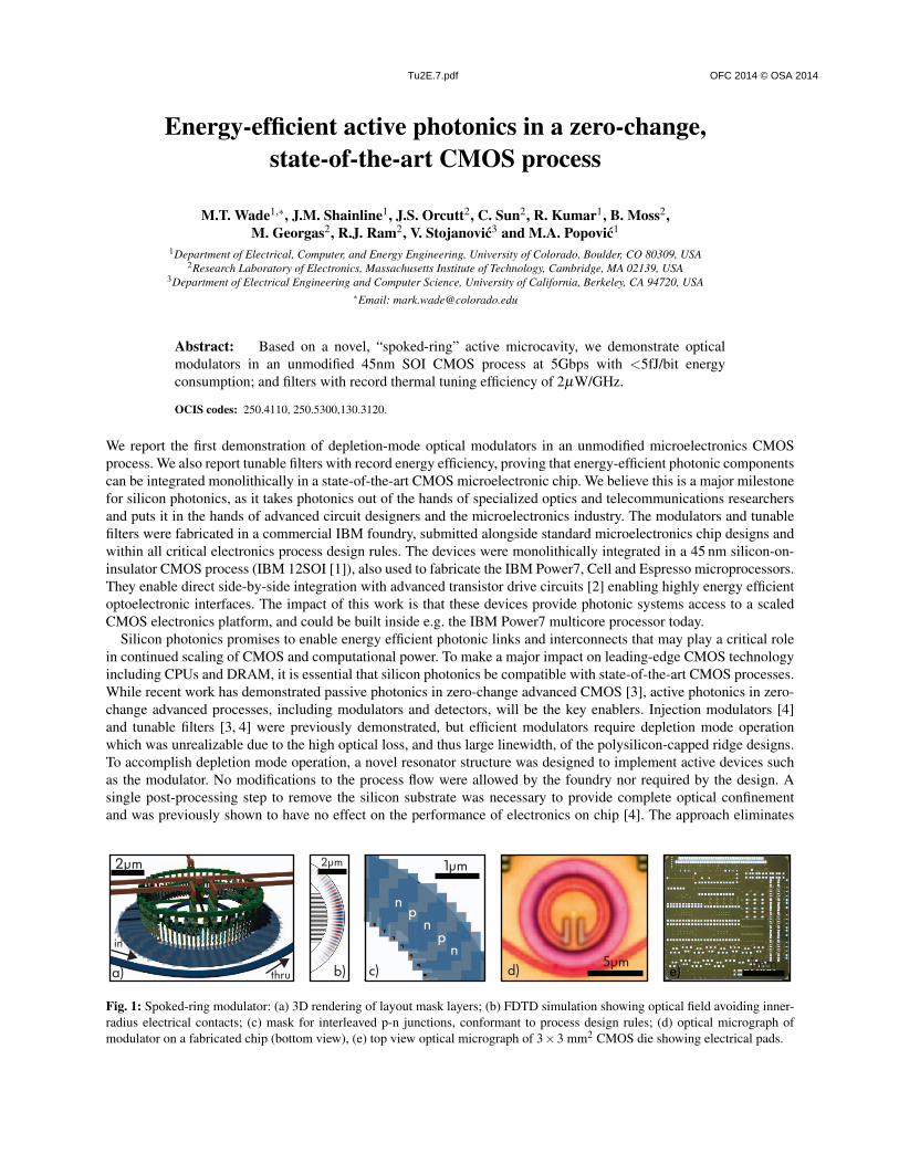
Fig. 1: Spoked-ring modulator: (a) 3D rendering of layout mask layers; (b) FDTD simulation showing optical field avoiding inner-radius electrical contacts; (c) mask for interleaved p-n junctions, conformant to process design rules; (d) optical micrograph ofmodulator on a fabricated chip (bottom view), (e) top view optical micrograph of 3×3 mm2 CMOS die showing electrical pads.
Tu2E.7.pdf OFC 2014 © OSA 2014
1280 1285 1290 1295 1300 1305 1310 1315 1320 1325 1330
−12
−10
−8
−6
−4
−2
0
Rela
tive
Tran
smis
sion
(dB)
3.3 THz
Wavelength (nm)
1300.72 1300.8 1300.88−12
−8
−4
0
0.5V0V-0.5V
3.2 THz
1260 1265 1270 1275 1280 1285 1290 1295 1300 1305 1310
−12
−10
−8
−6
−4
−2
0Re
lativ
e Tr
ansm
issi
on (d
B)
Wavelength (nm)
1263.25 1263.35 1263.45
0.6V0V-4V−12
−8
−4
0
a) b)
0µW
3µW
10µW
5.2dB
0µW7.6µW
41.2µW
7.3dB
c)d)
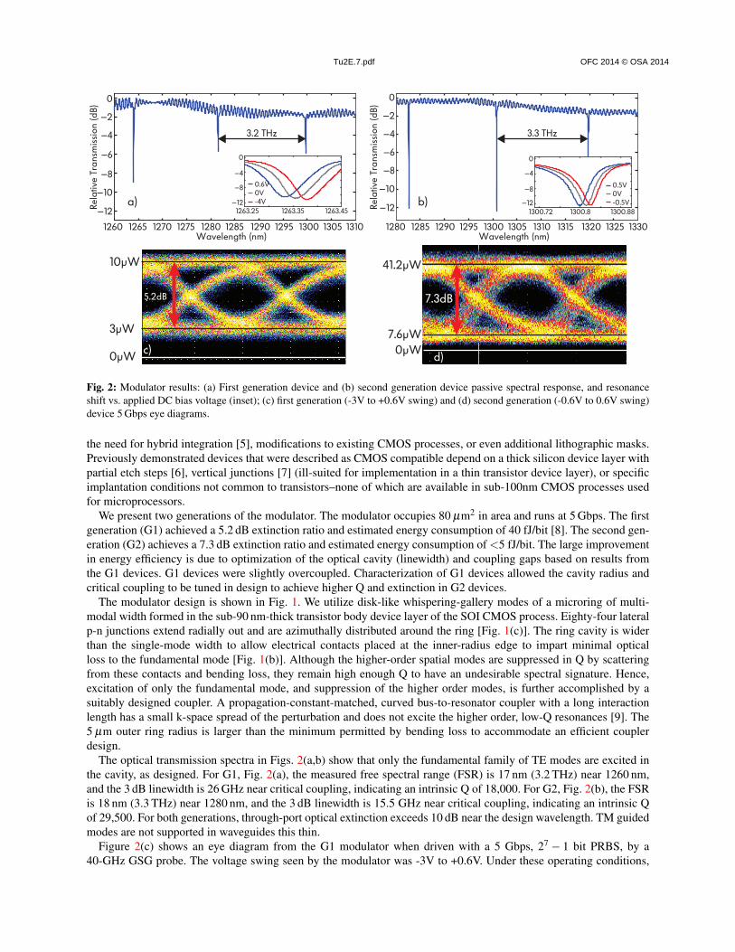
Fig. 2: Modulator results: (a) First generation device and (b) second generation device passive spectral response, and resonanceshift vs. applied DC bias voltage (inset); (c) first generation (-3V to +0.6V swing) and (d) second generation (-0.6V to 0.6V swing)device 5 Gbps eye diagrams.
the need for hybrid integration [5], modifications to existing CMOS processes, or even additional lithographic masks.Previously demonstrated devices that were described as CMOS compatible depend on a thick silicon device layer withpartial etch steps [6], vertical junctions [7] (ill-suited for implementation in a thin transistor device layer), or specificimplantation conditions not common to transistors–none of which are available in sub-100nm CMOS processes usedfor microprocessors.
We present two generations of the modulator. The modulator occupies 80 µm2 in area and runs at 5 Gbps. The firstgeneration (G1) achieved a 5.2 dB extinction ratio and estimated energy consumption of 40 fJ/bit [8]. The second gen-eration (G2) achieves a 7.3 dB extinction ratio and estimated energy consumption of <5 fJ/bit. The large improvementin energy efficiency is due to optimization of the optical cavity (linewidth) and coupling gaps based on results fromthe G1 devices. G1 devices were slightly overcoupled. Characterization of G1 devices allowed the cavity radius andcritical coupling to be tuned in design to achieve higher Q and extinction in G2 devices.
The modulator design is shown in Fig. 1. We utilize disk-like whispering-gallery modes of a microring of multi-modal width formed in the sub-90 nm-thick transistor body device layer of the SOI CMOS process. Eighty-four lateralp-n junctions extend radially out and are azimuthally distributed around the ring [Fig. 1(c)]. The ring cavity is widerthan the single-mode width to allow electrical contacts placed at the inner-radius edge to impart minimal opticalloss to the fundamental mode [Fig. 1(b)]. Although the higher-order spatial modes are suppressed in Q by scatteringfrom these contacts and bending loss, they remain high enough Q to have an undesirable spectral signature. Hence,excitation of only the fundamental mode, and suppression of the higher order modes, is further accomplished by asuitably designed coupler. A propagation-constant-matched, curved bus-to-resonator coupler with a long interactionlength has a small k-space spread of the perturbation and does not excite the higher order, low-Q resonances [9]. The5 µm outer ring radius is larger than the minimum permitted by bending loss to accommodate an efficient couplerdesign.
The optical transmission spectra in Figs. 2(a,b) show that only the fundamental family of TE modes are excited inthe cavity, as designed. For G1, Fig. 2(a), the measured free spectral range (FSR) is 17 nm (3.2 THz) near 1260 nm,and the 3 dB linewidth is 26 GHz near critical coupling, indicating an intrinsic Q of 18,000. For G2, Fig. 2(b), the FSRis 18 nm (3.3 THz) near 1280 nm, and the 3 dB linewidth is 15.5 GHz near critical coupling, indicating an intrinsic Qof 29,500. For both generations, through-port optical extinction exceeds 10 dB near the design wavelength. TM guidedmodes are not supported in waveguides this thin.
Figure 2(c) shows an eye diagram from the G1 modulator when driven with a 5 Gbps, 27 − 1 bit PRBS, by a40-GHz GSG probe. The voltage swing seen by the modulator was -3V to +0.6V. Under these operating conditions,

Tu2E.7.pdf OFC 2014 © OSA 2014
1301 1302 1303 1304
−12
−10
−8
−6
−4
−2
0
Wavelength (nm)
ThruDrop
a)
75GHz
<0.5dB
Rela
tive
Tran
smis
sion
(dB)
in thru
drop heater wires
P-well doped cavityc)
1300 1304 1308 1312 1316
−6
−5
−4
−3
−2
−1
0
0 mW0.5 mW1.2 mW2.4 mW3.5 mW5.2 mW
Rela
tive
Tran
smis
sion
(dB)
b)
Wavelength (nm)
Power (mW)0
5
10
15
1 2 3 4 5
Δλ0 (
nm)
Fig. 3: Partially spoked ring microcavity tunable filter: (a) Drop and through port spectral responses (0.5 dB IL, 75 GHz bandwidth),(b) thermally tuned drop-port spectra, showing 2.73 nm/mW tuning power vs. wavelength (inset), (c) 3D rendering of device layout.
5.2 dB modulation depth was measured with 4.5 dB insertion loss. The average switching energy (1/4CV 2pp for NRZ
data) is estimated from the voltage swing and a computed device capacitance of 12 fF to be 40 fJ/bit, assuming fullvoltage doubling (worst case). Figure 2(d) shows a 5 Gbps eye diagram from the G2 modulator. The voltage swingwas -0.6V to +0.6V. The G2 modulator achieved 7.3 dB modulation depth with 3 dB insertion loss and <5fJ/bit energyconsumption. This is comparable to state-of-the-art custom-process devices [7], and shows that high-performance de-vices can be designed with no process changes by leveraging advanced lithography and innovations in device topology.Furthermore, through monolithic integration and low-voltage operation, these devices promise very low driver circuitcomplexity and link energy-cost [2].
In a WDM transmitter, modulators are multiplexed on a bus waveguide, each tuned to a wavelength channel. Foractive wavelength tuning, a resistive microheater was integrated in the modulator cavity. The heater is also formed inthe body silicon layer and employs the process source/drain implants to give a 10 kΩ resistance. While tuning on theorder of a channel spacing (≈1 nm) is needed, these modulators achieve tuning over a full FSR with tuning efficienciesof 1.6 nm/mW (3.4 µW/GHz) [8].
Also critical to WDM communication links are efficient tunable demultiplexing filters. Based on a similar cavity asthe modulators, we demonstrate ultra-efficient thermally tunable filters. The cavity is doped with a mid-level p-typetransistor well implant which allows the cavity itself to be conductive without introducing excess optical loss. Fig. 3(a)shows a passive spectrum which shows <0.5 dB insertion loss and a 3 dB BW of 75 GHz. The tuning efficiency,shown in Figs. 3(b,c), is 2.73 nm/mW (2 µW/GHz) near 1300 nm – to the best of our knowledge a record efficiencyfor integrated filters.
We demonstrated <5fJ/bit modulation as well as thermally tunable filters with 2 µW/GHz efficiency in a novel“spoked-ring” microcavity fabricated in a commercial 45 nm CMOS logic process. This demonstration of ultra-energy efficient active devices, with no process modifications, is a potential watershed milestone towards enablingcomplete optical links monolithically integrated with advanced CMOS electronics, and implemented directly in exist-ing advanced-node CMOS foundries.
This work was supported by DARPA POEM program award HR0011-11-C-0100 and by an NSF Graduate ResearchFellowship Program (GRFP) award.
References
1. S. Lee, et al. IEEE International Electron Devices Meeting, pp. 255–258 (2007).2. B.R. Moss, et al. International Solid-State Circuits Conference, pp. 126–127 (2013).3. J.S. Orcutt, et al. Opt. Express 19, 2335 (2011).4. J.S. Orcutt, et al. Opt. Express 20, 12222 (2012).5. J. Hofrichter, et al. Opt. Express 20, 9363 (2012).6. J.C. Rosenberg, et al. Opt. Express 20, 26511 (2012).7. M.R. Watts, et al. Opt. Express 19, 21989 (2011).8. J.M. Shainline, et al. Opt. Lett. 38 (15), pp. 2657-2659 (2013).9. M. Chin and S. Ho, J. Lightwave Technol. 16, 1433 (1998).