Embed Size (px)
Citation preview

EMPro Workshop Version 4.0 Updated Feb, 2015

Page Agenda
– Introduction
– Getting started with the standalone EMPro EM simulation work flow with examples
– Getting started with EMPro 3D component work flow in ADS with examples
– 3D Solid modeling basic in EMPro
– Advanced Topics
2 Copyright © Keysight Technologies

Page 3/27/2015
Introduction
3 Copyright © Keysight Technologies

Page
What is “EM Simulations”?
– Electro-Magnetic simulation is numerical analysis technique that solves electro-magnetic field distribution problems, described by Maxwell equations
Copyright © Keysight Technologies 4
Differential Form Integral Form
Note * : The tables are from Wikipedia
*

Page
Common Numerical Analysis Techniques
5
FDTD
FEM MoM 3D Planar structures Full Wave and Quasi-Static Dense & Compressed Solvers Frequency Domain Multiport simulation at no additional cost High Q
3D Arbitrary Structures Full Wave EM Simulation Direct, Iterative Solvers Frequency Domain EM Multiport simulation at no additional cost High Q
3D arbitrary structures Full Wave EM simulations Handles much larger and complex problems Time Domain EM Simulate full size cell phone antennas EM simulations per each port GPU based hardware acceleration
FDTD ( Finite Difference Time Domain ) FEM ( Finite Element Method ) MoM ( Method of Moment )
Copyright © Keysight Technologies

Page
Common Numerical Analysis Techniques
6
FDTD
FEM MoM
FDTD ( Finite Difference Time Domain ) FEM ( Finite Element Method ) MoM ( Method of Moment )
EMPro’s Embedded Simulation Engines
Copyright © Keysight Technologies

Page
Common Numerical Analysis Techniques
7
FDTD
FEM MoM
ADS’s Embedded Simulation Engines
FDTD ( Finite Difference Time Domain ) FEM ( Finite Element Method ) MoM ( Method of Moment )
Copyright © Keysight Technologies
Page
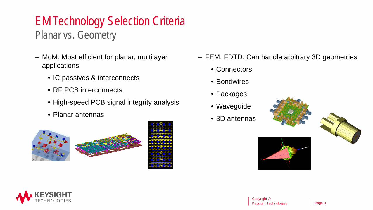
EM Technology Selection Criteria
– MoM: Most efficient for planar, multilayer applications
• IC passives & interconnects
• RF PCB interconnects
• High-speed PCB signal integrity analysis
• Planar antennas
– FEM, FDTD: Can handle arbitrary 3D geometries
• Connectors
• Bondwires
• Packages
• Waveguide
• 3D antennas
Planar vs. Geometry
8 Copyright © Keysight Technologies

Page
EM Technology Selection Criteria
– MoM, FEM
• Solves natively in the frequency domain
• Best for high Q applications - RF/MW filters - Oscillators
– FDTD
• Solves natively in the time domain
• Best for TDR, EMI analysis - Signal Integrity - Transitions
Response/Analysis Type
9 Copyright © Keysight Technologies

Page
EM Technology Selection Criteria
– FEM
• Most efficient for multi-port applications
• Solves for all ports in a single simulation - Packages - Interconnect networks
– FDTD
• Most efficient for high number of mesh cells
• Use a sequence of direct calculations instead of matrix solve
• Highly parallelized, can take advantage of GPU acceleration
- Antenna placement on autos, planes - Bio analysis with complex human body
models (e.g., SAR)
Device Complexity/Problem Size
10 Copyright © Keysight Technologies
Page
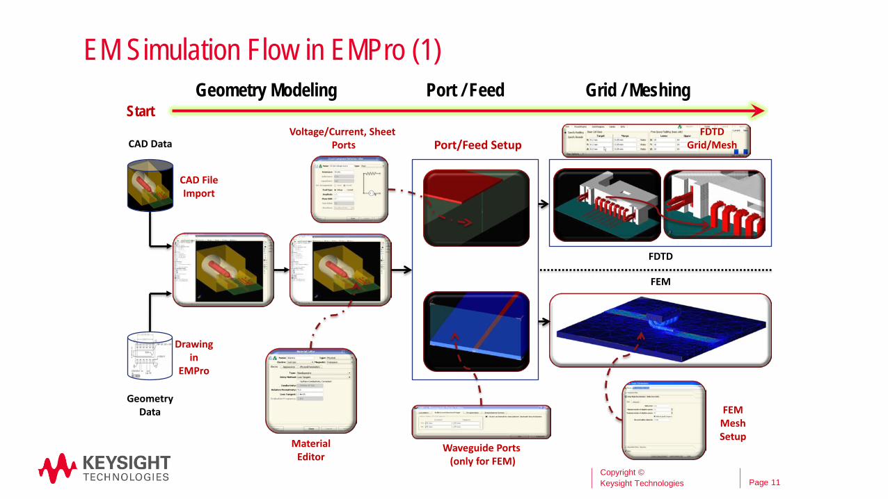
EM Simulation Flow in EMPro (1)
11
CAD File Import
Geometry Data
CAD Data
Drawing in
EMPro
Material Editor
Port/Feed Setup
Waveguide Ports (only for FEM)
Voltage/Current, Sheet Ports
FDTD Grid/Mesh
Geometry Modeling Grid / Meshing
FEM Mesh Setup
FDTD
FEM
Start Port / Feed
Copyright © Keysight Technologies
Page
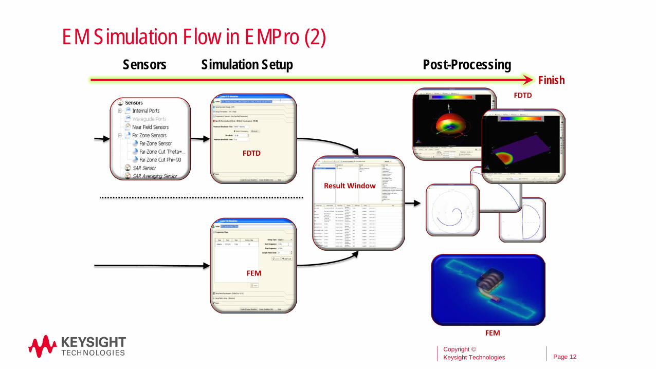
EM Simulation Flow in EMPro (2)
12
Sensors Simulation Setup
FEM
FDTD
Post-Processing
Result Window
FEM
FDTD
Finish
Copyright © Keysight Technologies

Page
EMPro Graphical User Interface (GUI)
13
WorkSpace Window
Project Tree: • Port/Feed • Sensors • Materials • Waveforms • Boundary • Grid/Mesh • Python Script
Customizable Tool Bars
View Tools (Under View
menu as well)
Workspace Tool Bar
Geometry Tools Simulator
Toggle Button
Copyright © Keysight Technologies
Page 3/27/2015
Standalone EMPro EM Simulation Work Flow With Examples
14 Copyright © Keysight Technologies
Page
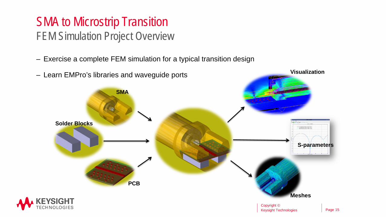
SMA to Microstrip Transition
– Exercise a complete FEM simulation for a typical transition design
– Learn EMPro’s libraries and waveguide ports
FEM Simulation Project Overview
15
SMA
Solder Blocks
PCB
Visualization
Meshes
S-parameters
Copyright © Keysight Technologies
Page
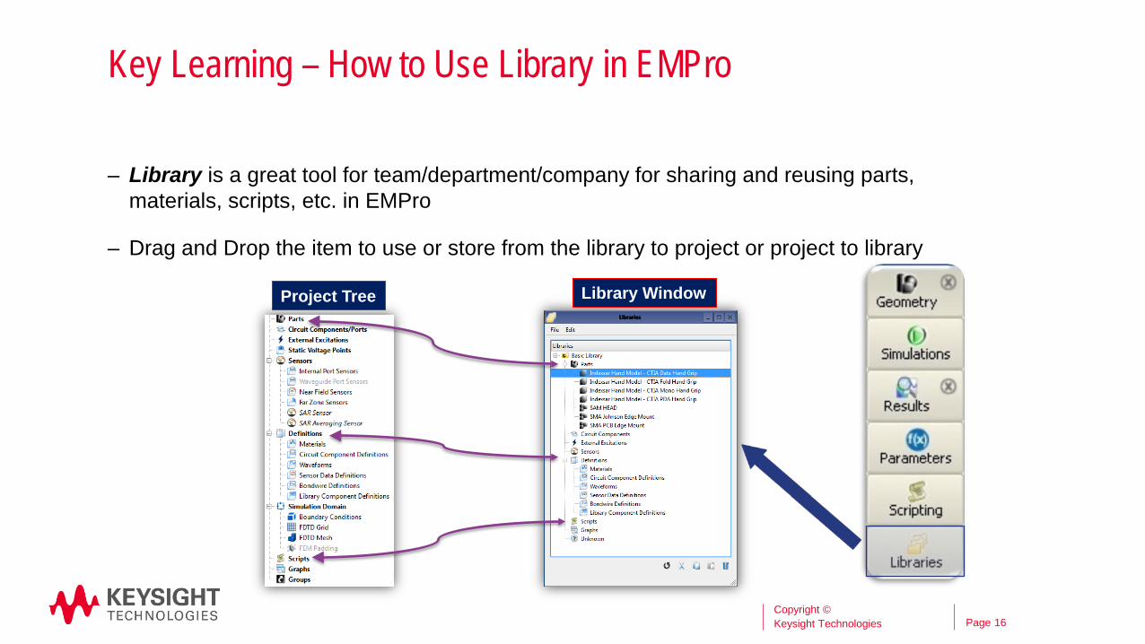
Key Learning – How to Use Library in EMPro
– Library is a great tool for team/department/company for sharing and reusing parts, materials, scripts, etc. in EMPro
– Drag and Drop the item to use or store from the library to project or project to library
16
Project Tree Library Window
Copyright © Keysight Technologies

Page
Key Learning – How to Create Waveguide Ports
– Waveguide ports are fully calibrated 2-dimensional planar source
– Waveguide ports could be either nodal or modal excitation
– Creating a waveguide port using “EMPro Waveguide Ports Editor”: 1. Location: Select or choose a 2D face on object where the waveguide port will be
located 2. EditCrossSectionPage: Size the port by entering numbers for u, v extension
from the selected face 3. Properties: Define nodal or modal, and number of modes 4. Impedance Lines: Define impedance lines to calculate port impedance
17
Project tree
Copyright © Keysight Technologies
Page
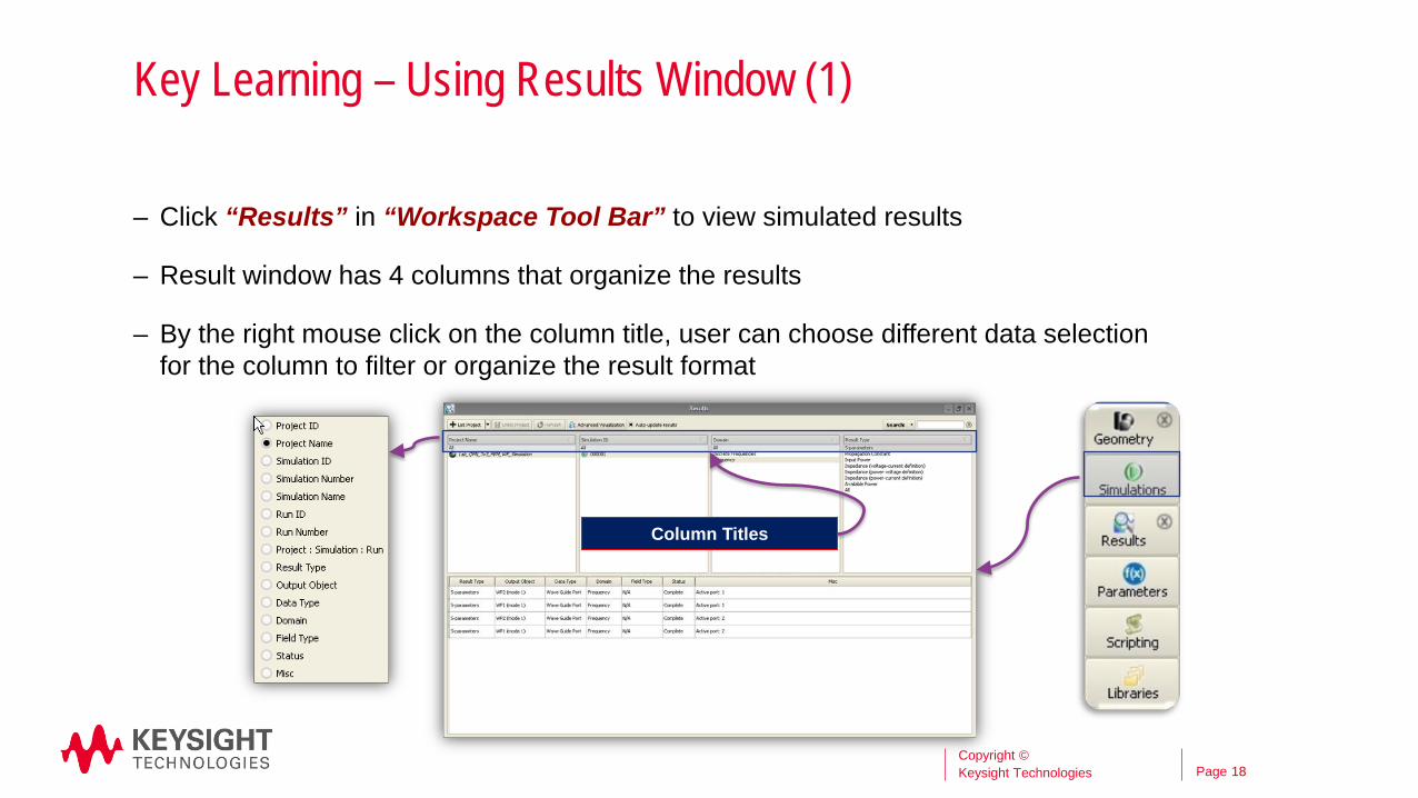
Key Learning – Using Results Window (1)
– Click “Results” in “Workspace Tool Bar” to view simulated results
– Result window has 4 columns that organize the results
– By the right mouse click on the column title, user can choose different data selection for the column to filter or organize the result format
18
Column Titles
Copyright © Keysight Technologies
Page
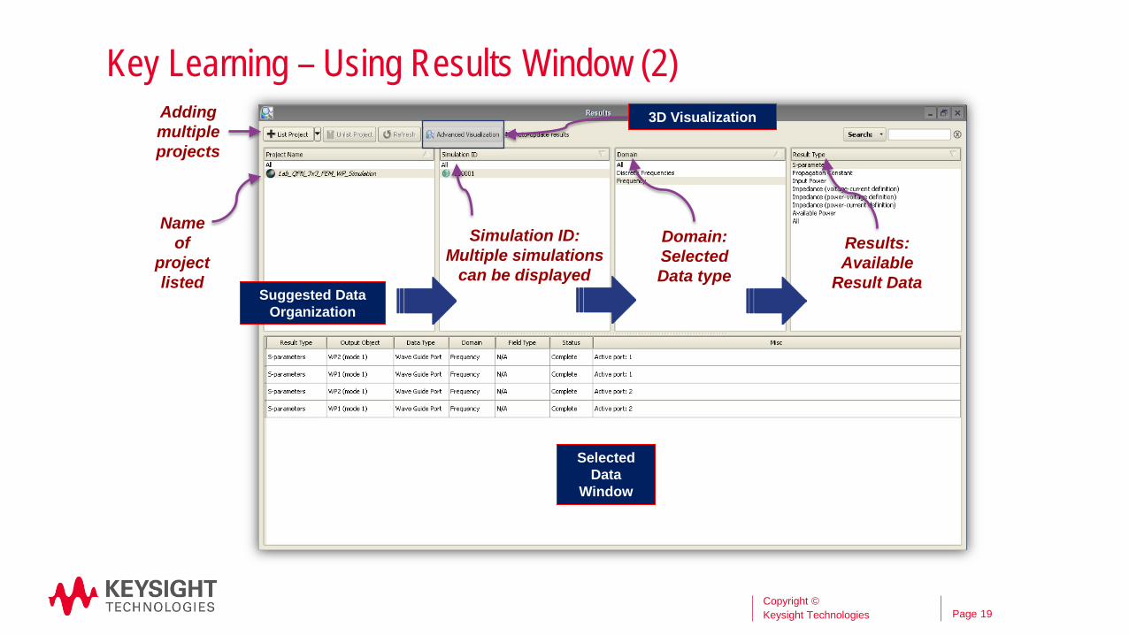
Key Learning – Using Results Window (2)
19
Adding multiple projects
Name of
project listed
Simulation ID: Multiple simulations
can be displayed
3D Visualization
Domain: Selected Data type
Results: Available
Result Data
Selected Data
Window
Suggested Data Organization
Copyright © Keysight Technologies

Page
Instructor Demo
20 Copyright © Keysight Technologies

Page
– Project Setup Project to use: “SMA to Microstrip Transition Board Only.ep”
Library to add: “EMPro_Workshop_Library”
Parts from library to use: “SMA Johnson Edge Mount with Thick Legs” and “Solder Block”
Port type: “Waveguide Port” and “50 Ohm Source”
– Simulation Setup Simulation Engine: “FEM”
Simulation frequencies and sweep: “1 ~ 30 GHz and Adaptive Freq Sweep”
Simulation Accuracy (Delta-S): 0.02 (2%)
Solver: “Direct Solver”
– Tasks Create two waveguide ports (SMA input and PCB microstrip output)
Use “EMPro_Workshop_Library” to place SMA connector on the board
Plot S-parameters
Lab Exercise Description
21
Reference Impedance
Copyright © Keysight Technologies

Page
Coax to Waveguide Transition
– Exercise a FEM simulation for a typical waveguide transition design
– Learn parametric modeling in EMPro
FEM Simulation Project Overview
22
Visualization
Meshes
S-parameters
Parameters
Copyright © Keysight Technologies

Page
Key Learning – Plotting Multiple S11 Results for Comparison
23
– Select multiple simulation results from “Simulation ID” with “Ctrl” button or select “All” – This also can be applied to multiple data from different projects
– Select “Frequency” from “Domain”
– Select “S-Parameters” from “Result Type”
– Select two “S11” from “Data Window” with “Ctrl” button
– Plot with “Line Graph”
Copyright © Keysight Technologies

Page
Key Learning – Visualizing E/H Field and Meshes
24
Enable Advance Visualization by selecting the project name
– Advanced Visualization is a special tool to visualize objects, meshes, E/H field plots in 3D, as well as far field radiation patterns from FEM simulation results
– Enable or start it by selecting the project
Copyright © Keysight Technologies

Page
Instructor Demo
25 Copyright © Keysight Technologies

Page
Lab Exercise Description
26
– Project Setup Project to use: “FEM - Coax to Waveguide Transition.ep”
Port type: “Waveguide Port” and “50 Ohm Source”
– Simulation Setup Simulation Engine: “FEM”
Simulation frequencies and sweep: “8 ~ 12.5GHz Adaptive Freq Sweep and 10GHz Single Frequency”
Set “Field Storage” to “User Defined Frequencies” to store the field data only at the specified frequencies
Simulation Accuracy (Delta-S): 0.01 (1%)
Solver: “Direct Solver”
– Tasks Simulate the design with two different disc sizes. Plot the results on the same graph and visualize the E-field data on vertical
cut plane
- disk_r = 1 mm
- disk_r = 1.8 mm
Copyright © Keysight Technologies

Page
Quasi-Yagi Antenna * FEM Simulation Project Overview
27
Visualization
Meshes
S-parameters
* : “Simple Broadband Planar CPW-Fed Quasi-Yagi Antenna” H. K. Kan, Member, IEEE, R. B. Waterhouse, Senior Member, IEEE, A. M. Abbosh, and IEEE, A. M. Abbosh, and M. E. Bialkowski, Fellow, IEEE
– Exercise a complete FEM simulation for an antenna design
– Learn how to create far zone sensors and plot antenna data
Copyright © Keysight Technologies
Page
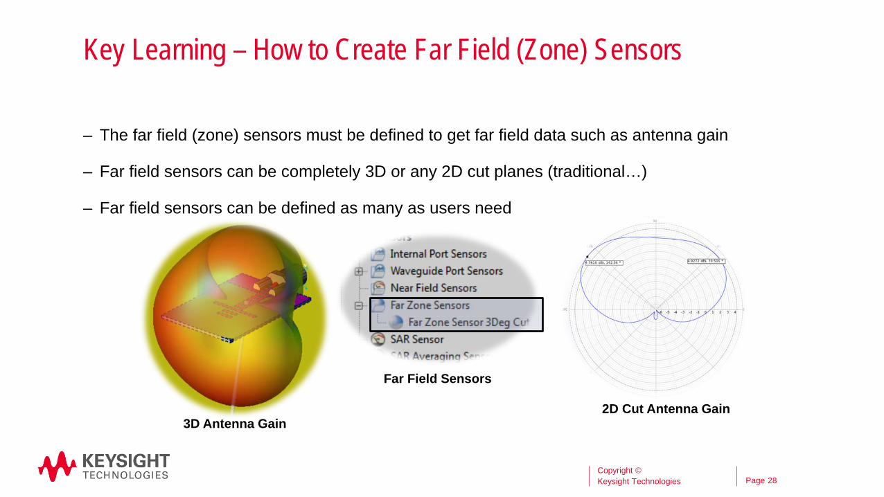
Key Learning – How to Create Far Field (Zone) Sensors
– The far field (zone) sensors must be defined to get far field data such as antenna gain
– Far field sensors can be completely 3D or any 2D cut planes (traditional…)
– Far field sensors can be defined as many as users need
28
Far Field Sensors
3D Antenna Gain 2D Cut Antenna Gain
Copyright © Keysight Technologies

Page
Instructor Demo
29 Copyright © Keysight Technologies

Page
Lab Exercise Description
– Project Setup
Project to use: “FEM - Quasi-Yagi Antenna.ep” Port type: “Waveguide Port” and “50 Ohm Source”
– Simulation Setup
Simulation Engine: “FEM” Simulation frequencies and sweep: “7-13 GHz and Adaptive Freq Sweep and Single Freq at 10 GHz” Simulation Accuracy (Delta-S): 0.02 (2%)
Edge meshing (0.2 mm) on transmission lines
Solver: “Direct Solver”
– Tasks
Define a far field sensor, full 3D
Plot S11 and antenna gain on 2D
30 Copyright © Keysight Technologies

Page
Via Clearance TDR
– Exercise a complete FDTD TDR simulation (Instantaneous TDR) for a typical transition design
– Learn how to setup FDTD TDR simulation and use passive loads
FDTD Simulation Project Overview
31
Meshes
TDR Respond
Copyright © Keysight Technologies

Page
Key Learning – Setting up FDTD Simulation Timestep for TDR
– FDTD TDR is instantaneous TDR, which means it’s not based on the broadband s-parameters data. It directly calculates the instantaneous voltages and currents on the structure, then computes the impedance, V/I.
FDTD TDR produces very fast TDR result since it only requires the signal (step source) to travel to the discontinuity and back to the excited port.
It is not limited by the band limited s-parameters.
– Initial glitch on TDR response
Since the instantaneous TDR response is directly calculated from V/I, it reveals the initial glitch on TDR response. It is due to the zero current flowing through at the time = 0
32 Copyright © Keysight Technologies
Page
Key Learning – Loads in FDTD
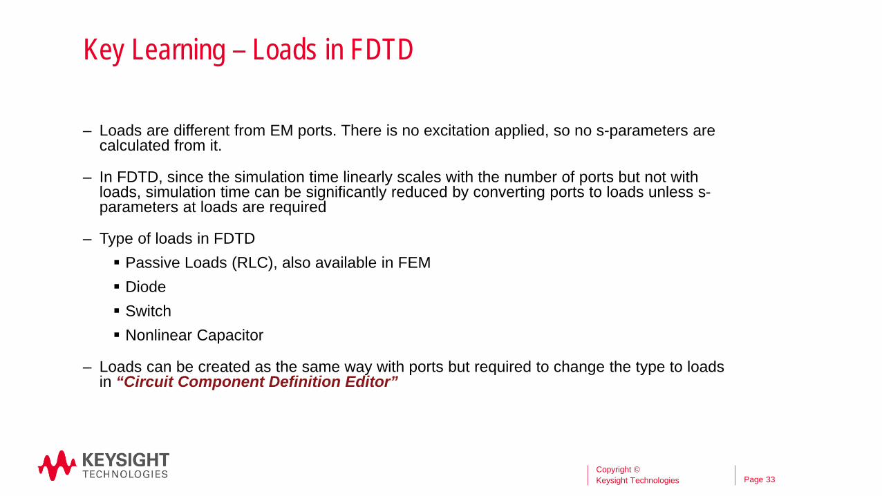
– Loads are different from EM ports. There is no excitation applied, so no s-parameters are calculated from it.
– In FDTD, since the simulation time linearly scales with the number of ports but not with loads, simulation time can be significantly reduced by converting ports to loads unless s-parameters at loads are required
– Type of loads in FDTD Passive Loads (RLC), also available in FEM Diode Switch Nonlinear Capacitor
– Loads can be created as the same way with ports but required to change the type to loads in “Circuit Component Definition Editor”
33 Copyright © Keysight Technologies

Page
Instructor Demo
34 Copyright © Keysight Technologies

Page
Lab Exercise Description
– Project Setup Project to use: “FDTD - Via Clearance TDR.ep” Port type: “50 Ohm Voltage Source” Load type: “100 Ohm Resistor”
– Simulation Setup Simulation Engine: “FDTD” Uncheck “Detect Convergence” Simulation timestep: “2000 timesteps”
– Tasks Change the load impedance to 200 ohm to see different load discontinuity Plot TDR result
35 Copyright © Keysight Technologies

Page
Monopole Antenna
– Exercise a complete FDTD simulation for a typical antenna design
– Learn the parametric EMPro simulation
– Learn how to visualize FDTD meshes (3D & 2D)
FDTD Simulation Project Overview
36
Meshes
Antenna Gain
Copyright © Keysight Technologies
Page
Key Learning – FDTD Mesh Visualization
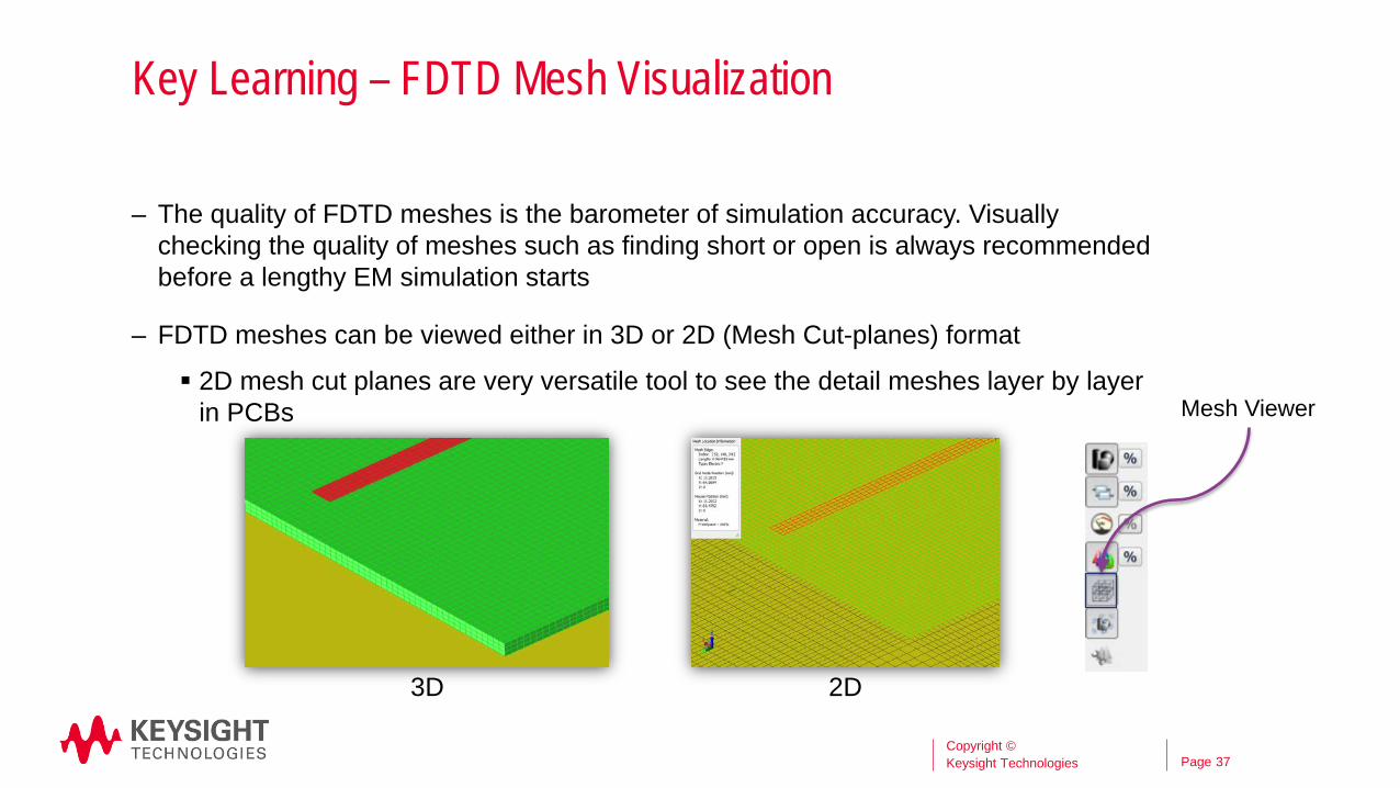
– The quality of FDTD meshes is the barometer of simulation accuracy. Visually checking the quality of meshes such as finding short or open is always recommended before a lengthy EM simulation starts
– FDTD meshes can be viewed either in 3D or 2D (Mesh Cut-planes) format
2D mesh cut planes are very versatile tool to see the detail meshes layer by layer in PCBs
37
Mesh Viewer
3D 2D
Copyright © Keysight Technologies

Page
Key Learning – FDTD Parametric Simulation
– EMPro’s parameterized modeling allows users to do parametric EM simulations
– Multiple parameters can be swept for EM simulations
– The port locations can be automatically anchored between the center edge of copper strip and the ground plane while parameterization
38
Port Location
Copyright © Keysight Technologies

Page
Instructor Demo
39 Copyright © Keysight Technologies

Page
Lab Exercise Description
– Project Setup Project to use: “FDTD - Monopole on PCB.ep” Port type: “50 Ohm Voltage Source”
– Simulation Setup Simulation Engine: “FDTD” Check “Perform Parameter Sweep”
oSweep: 20 ~ 22 mm for the length of monopole antenna, with 5 points Simulation timestep: “10000 timesteps”
– Tasks • Understand how to visualize FDTD meshes, 2D and 3D • Perform FDTD parametric simulations
40 Copyright © Keysight Technologies

Page
Magnetron Eigen-Mode
– Exercise Eigen mode analysis for a typical cavity structure
– Learn how to plot Eigen frequencies and Q values
Simulation Project Overview
41
Eigen Frequencies & Q value
Field Plot
Copyright © Keysight Technologies

Page
Key Learning – Eigen Mode Simulation Setup
– Closed boundary simulations
ABC boundary is not allowed
– Simulation setup is similar to what FEM simulation setup is except;
“Start frequency” : is an estimate for the first eigen frequency to be calculated
“Number of eigenmodes” : is how many eigen frequencies calculated
– Plots Eigen frequencies and Q values
42 Copyright © Keysight Technologies

Page
Instructor Demo
43 Copyright © Keysight Technologies

Page
Lab Exercise Description
– Project Setup Project to use: “Eigen - Magnetron.ep” Port type: None
– Simulation Setup Simulation Engine: “FEM Eigenmode Simulation” Start frequency: “9 GHz” Number of eigenmodes: “20”
– Tasks Plot the E/H field on the first two eigen frequencies Plot the Q values
44 Copyright © Keysight Technologies

Page
2D Port Solver
– Exercise 2D port analysis
– Learn how to plot field data and propagation constant
Simulation Project Overview
45
Propagation Constant at Port 1
E field H field Copyright © Keysight Technologies

Page
Key Learning – 2D Port Simulation Setup and Field Data
– 2D port simulation can be performed either at “EMPro Waveguide Ports Editor” window or “FEM 2D Port Simulation” window
– In order to get the higher order modes, the number of modes in the port setup window should be set accordingly
– The field plot is displayed in the native EMPro window not Advanced Visualization window
46 Copyright © Keysight Technologies

Page
Instructor Demo
47 Copyright © Keysight Technologies

Page
Lab Exercise Description
– Project Setup
Project to use: “Port – SMA Connector.ep”
Port type: Waveguide Port
– Simulation Setup
Simulation Engine: “FEM 2D Port Simulation”
Simulation frequencies and sweep: “0-20 GHz and Adaptive Freq Sweep”
Convergence: “Relative error in impedance = 0.01”
– Tasks
Understand how to plot propagation constant and field data
48 Copyright © Keysight Technologies
Page
Differential Pair with Slot on Ground Plane
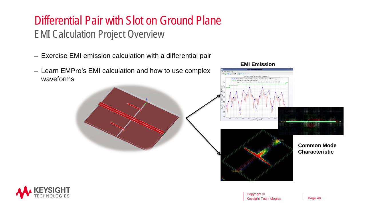
– Exercise EMI emission calculation with a differential pair
– Learn EMPro’s EMI calculation and how to use complex waveforms
EMI Calculation Project Overview
49
EMI Emission
Common Mode Characteristic
Copyright © Keysight Technologies

Page
Key Learning – Two Options for EMI Calculation (1)
Option1* : Post Processing Method, Faster Emission Calculation
– Plot emission vs. freq at discrete frequencies (faster)
o Run broadband s-parameter and far field simulation, no transient far zone
o Create or read the waveforms to excite sources
o Run EMI Calculation Add-on and assign ports with corresponding waveforms
o Plot (post-process) the E-field at the measuring angle with the specified distance such as 3 meters or 10 meters
o Overlay EMI Limits to the result
50
* : Both FEM/FDTD Simulation
Copyright © Keysight Technologies

Page
Key Learning – Two Options for EMI Calculation (2)
Option2* : Direct Computation Method, Longer Simulation Time
– Plot emissions vs. freq like a real measurement, but could be longer o Create or read the waveforms to excite sources
o Assign ports with corresponding waveforms
o Set simulations the simulation for enough periods of excited waveforms with FDTD and enter steady state frequencies (the more the better for the # of frequencies)
o Enable far zone sensors (only for measuring angles) and also set to collect transient far zone
o Simulate
o Plot the E-field at the measuring angle with the specified distance such as 3 meters or 10 meters
o Overlay EMI Limits to the result
51
* : FDTD Simulation Copyright © Keysight Technologies

Page
Key Learning – Using Complex Waveforms from CSV file format (3) – Custom waveforms can be used for EMI emission calculation
– Use “User Defined” for the type of waveform
– Import waveform data using “Import Waveform Data” to read any .csv or .txt file
52 Copyright © Keysight Technologies

Page
– Use “EMI Emission Calculation” under “Tools”
– Choose simulation ID that to be used for EMI calculation
– Choose appropriate sensor (far zone)
– Assign waveforms to ports
• Multiplier is used to change the mode of excitation, for example, use 1 and -1 to make differential
– Define distance for the calculation
– “Plot” the result
Key Learning – EMI Calculation with Option 1 (4)
53 Copyright © Keysight Technologies

Page
Instructor Demo
54 Copyright © Keysight Technologies

Page
Lab Exercise Description
– Project Setup Project to use: “EMI - Suppression with slot on ground sheet port.ep” Port type: “Sheet Port” and “50 Ohm Source”
– Simulation Setup Simulation Engine: “FEM” Simulation frequencies and sweep: “0.1 ~ 5 GHz and 25 freq points Linear Sweep” Simulation Accuracy (Delta-S): 0.02 (2%) Solver: “Iterative Solver”
– Tasks Run a simulation with a slot on the ground planes Calculate EMI emission at 3 meters with 100MHz pulse waveform Enable bypass capacitors and run a simulation Calculate EMI emission at 3 meters with 100MHz pulse waveform and compare to the result without
bypass capacitors
55
Copyright © Keysight Technologies

Page 3/27/2015
EMPro 3D Component Work Flow in ADS with Examples
56 Copyright © Keysight Technologies

Page
EMPro 3D Component in ADS
– What is it? • EMPro designs can be directly accessed from ADS as OA (Open Access) library
components
• All parameters from EMPro are transparent in ADS
• EMPro 3D component can be used both in ADS layout and schematic
• Layout lookalike symbol is automatically generated with pins
• Changes in EMPro are automatically reflected (synchronized) in ADS
– Where is it used? • Where circuits and EM designs need to be combined
• Where a parametric simulation (sweep) is required
• Where an optimization of 3D EM model is required
57
The EM design can be optimized for not only linear s-parameters but also non-linear design specifications such as IP3 or gain compression
Copyright © Keysight Technologies
Page
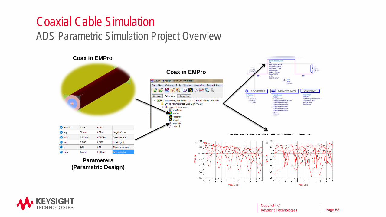
Coaxial Cable Simulation ADS Parametric Simulation Project Overview
58
Coax in EMPro
Parameters (Parametric Design)
Coax in EMPro
Copyright © Keysight Technologies

Page
Key Learning – Adding EMPro 3D Component (1)
– Add an EMPro design as a library in ADS • Only OA format EMPro projects can be used
• Use “DesignKits/Manage Libraries” from ADS Main
– EMPro 3D Component in ADS • EMPro design is added as an OA cell
• EMPro project can be opened directly from ADS
• EMPro 3D component can be used in ADS layout
• Automatically produce lookalike and symbol view for schematic use
59 Copyright © Keysight Technologies

Page
Key Learning – Using EMPro 3D Component (2)
– Drag and drop the lookalike symbol to ADS schematic like standard ADS components
– Pins and Port • Each port in EMPro is represented by two pins in ADS ( +, - or
reference pin ) • Ports are where data (s-parameters) is collected • Make sure not to mix them up
– EMPro 3D Component in Layout • EMPro model location at Z=0 is synced up with Z=0 location in ADS
stackup • The location for Z can be controlled by “CustomComponentOffsetZ”
parameter
60 Copyright © Keysight Technologies

Page
Key Learning – EM Model for Parametric Simulations (3)
– EM model view is automatically created when the EMPro 3D Component is simulated in ADS
– Any simulation of EMPro 3D Components builds EM model data, which can be re-used or can be interpolated in other simulations
• It only allows linear interpolation of data
• In the “Interpolation” tab, “Use Interpolation” should be turn on to be re-used
– Multi-Dimensional sweep is allowed • Use simple multiple parameter sweep simulation in ADS
61 Copyright © Keysight Technologies

Page
Instructor Demo
62 Copyright © Keysight Technologies

Page
Lab Exercise Description
– Project Setup
ADS Project to use: “EMPro_3D_Comp_Para_Coax_wrk” EMPro Library to add: “EMPro_3D_Components_Library” Open “TestBench” schematic and drag/drop the lookalike symbol of “Parameterized_Coax” and
complete the schematic as shown above
– Simulation Setup
Simulation setting from EMPro project will be automatically used o Solver selection o Basis function o Simulation Accuracy (Delta-S)
– Tasks
Add EMPro 3D component library to ADS workspace
Use EMPro 3D component in ADS schematic
Run a simulation from ADS schematic with Er=2.2 ~ 2.4, 3 pts parametrics simulation
Plot S-parameters (S11 and S21) vs. freq with various Er values
63
Copyright © Keysight Technologies

Page
Strip to Via Transition Optimization ADS Optimization Project Overview
64
Strip to Via Transition
Parameters (Parametric Design)
“Strip to Via” in EMPro
Copyright © Keysight Technologies
Page
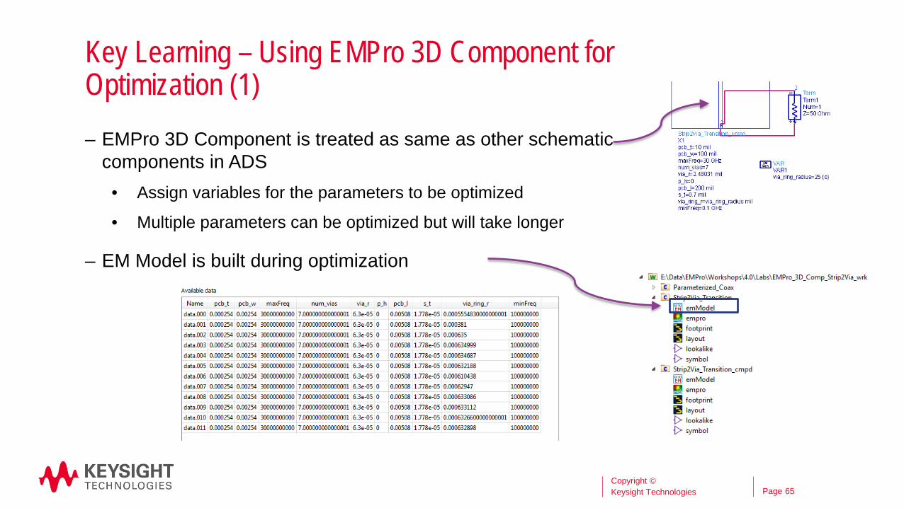
Key Learning – Using EMPro 3D Component for Optimization (1) – EMPro 3D Component is treated as same as other schematic
components in ADS • Assign variables for the parameters to be optimized
• Multiple parameters can be optimized but will take longer
– EM Model is built during optimization
65 Copyright © Keysight Technologies

Page
Key Learning – Setup and Run Optimization (2)
– Optimization setup for EMPro 3D Component is exactly same as in ADS
• Setup goals. In this case, the return loss, S11 and S22, lower than -30dB are goals to achieve
• Choose optimizer or optimization technology
– Running optimization • Click “Optimize” button to run
66 Copyright © Keysight Technologies

Page
Instructor Demo
67 Copyright © Keysight Technologies

Page
Lab Exercise Description
– Project Setup
ADS Project to use: “EMPro_3D_Comp_Strip2Via_wrk”
EMPro Library to add: “EMPro_3D_Components_Library”
Open “TestBench” schematic and drag/drop the lookalike symbol of “Strip2Via_Transition” and complete the schematic
– Simulation Setup
Simulation setting from EMPro project will be automatically used o Solver selection o Basis function o Simulation Accuracy (Delta-S)
– Tasks
Add EMPro 3D component library to ADS workspace
Use EMPro 3D component in ADS schematic
Set a variable to EMPro parameter “via_ring_r” to “via_ring_radius”
Set optimization values range from 18 to 24 and set the default to 20
Run an optimization
Plot optimized S-parameters (S11 and S21) vs. freq
68
Optimized: 21.8694 mil
Copyright © Keysight Technologies

Page 3/27/2015
3D Solid Modeling Basic in EMPro
69 Copyright © Keysight Technologies

Page
Three Key Basic Learning In 3D Solid Modeling
70
– Create
– Modify
– Origin/Orientation
Copyright © Keysight Technologies

Page
Create
71
– “Create” menu is to create a new 3D/2D model Three steps with using “Create” command for 3D solid modeling
1. Set the orientation of 3D model (where the object is located) 2. Create a 2D sketch such as rectangle, circle, etc. (the 2D sketch has to be completely
closed) 3. Extrusion: Sweep 2D sketch to a direction of extrusion to make it as a 3D object
Two steps with using “Create” command for 2D solid modeling Same as in 3D but without the third step
– Types of 2D sketches available Rectangle, Polygon, N-Sliced Polygon, Circle, Ellipse Others such as lines, arc, etc. can be combined to create any shape of 2D sketch
Copyright © Keysight Technologies

Page
Some Useful Tips in Creating 2D Sketches
– Trimming edges, “Trim Edges” , will trim the lines unused. Always make sure the 2D sketch is completely closed to avoid any warning or problems
– The “Select/Manipulate“ button must be on to select or manipulate edges, vertices, or constraints as well as moving vertices or edges
– Use entry window to enter coordinates: Press “Tab” button to active the entry window while you are in the 2D sketch window
72 Copyright © Keysight Technologies

Page
Some Useful Options in Create/Extrusion
– While executing the extrusion, advanced operations also can be applied, such as “Twist” or “Draft”
73
Twist
Draft By Angle Draft By Law Hole w/wo Draft Hole Special
Copyright © Keysight Technologies
Page
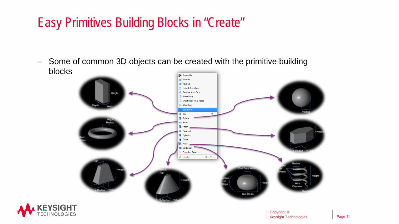
Easy Primitives Building Blocks in “Create”
– Some of common 3D objects can be created with the primitive building blocks
74 Copyright © Keysight Technologies

Page
Instructor Demo
75 Copyright © Keysight Technologies

Page
Modify
– “Modify” menu is to modify an existing 3D/2D solid model
– Select the object first that is to be modified in order to enable the modify menus
– Most of them are for 3D objects except “Offset Sheet Edges” and “Thicken Sheet”
76
Blending Chamfering Shelling Offset Edges Loft Faces
Copyright © Keysight Technologies

Page
Instructor Demo
77 Copyright © Keysight Technologies

Page
Lab Exercise Description for Create
– Start a new EMPro and exercise the followings
• Creating a box Create a box, 10x10x30 mm, on a default 2D sketch plane (XY plane) Name it as “Box1” in the “Parts” in the “Project Tree”
• Creating a cylinder Create a cylinder, 5 mm radius and 20 mm long, on a default 2D sketch plane
with “Tab” button Name it as “Cylinder1” in the “Parts” in the “Project Tree”
78 Copyright © Keysight Technologies

Page
Lab Exercise Description for Modify
– Blending the box: Blend an edge of “Box1”
– Chamfering the box: Chamfer an edge of “Box1”
– Shelling the box:
Any operation applied is stored under the object tree in EMPro
Select the chamfering and blending operation and remove (delete) them (going back to before…)
Apply the shell and select the top face to be open
Set the shell thickness to “1 mm”
79 Copyright © Keysight Technologies
Page
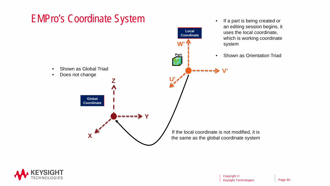
EMPro’s Coordinate System
80
Y
Z
X
U’
W’
Global Coordinate
V’
Local Coordinate
If the local coordinate is not modified, it is the same as the global coordinate system
• Shown as Global Triad • Does not change
• If a part is being created or an editing session begins, it uses the local coordinate, which is working coordinate system
• Shown as Orientation Triad Part
Copyright © Keysight Technologies

Page
EMPro’s Coordinate System
81
Y
Z
X
U’
W’
U
W
V Global Coordinate
V’
Reference Coordinate
Local Coordinate
• If a part is moved to or created from an assembly, the assembly’s coordinate becomes the reference coordinate
• The reference coordinate is only effective when an assembly is used
Part
Copyright © Keysight Technologies

Page
Working with Origin / Orientation
– When you want your local “U, V, and W” coordinate to be either on standard XY, YZ, or ZX plane, you can use “Presets” in “Specify Orientation”
– The default is XY plane
“Presets”
82 Copyright © Keysight Technologies
Page
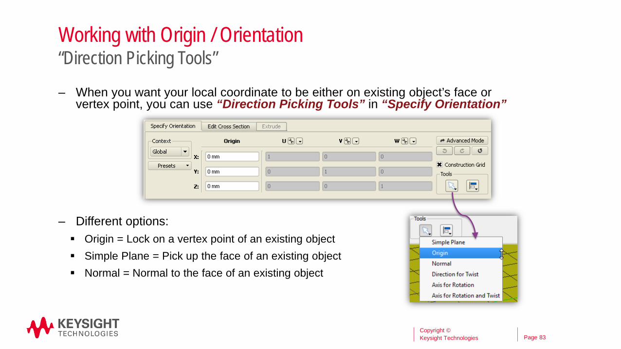
Working with Origin / Orientation
– When you want your local coordinate to be either on existing object’s face or vertex point, you can use “Direction Picking Tools” in “Specify Orientation”
– Different options: Origin = Lock on a vertex point of an existing object Simple Plane = Pick up the face of an existing object Normal = Normal to the face of an existing object
“Direction Picking Tools”
83 Copyright © Keysight Technologies
Page
Other Useful Geometry Tools
– Copy Copying part(s) works the same way as in Windows. Select a part(s) to copy and paste in “Parts”
under “Project Tree”
– Move Use “Modify/Transform/Translate” – Move the part by the specified or user entered distance Use “Specify/Orientation” – Move the part by moving the local coordinate of part
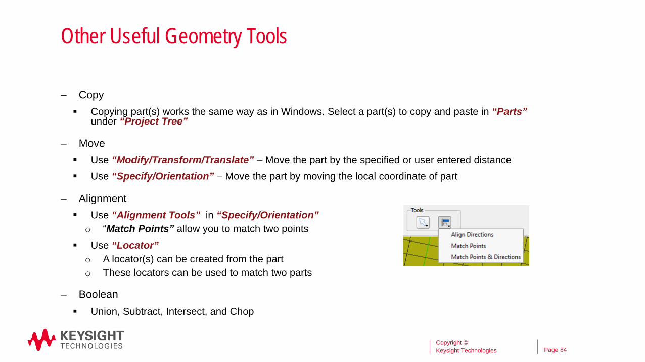
– Alignment Use “Alignment Tools” in “Specify/Orientation” o “Match Points” allow you to match two points
Use “Locator” o A locator(s) can be created from the part o These locators can be used to match two parts
– Boolean Union, Subtract, Intersect, and Chop
84 Copyright © Keysight Technologies

Page
Instructor Demo
85 Copyright © Keysight Technologies

Page
Lab Exercise Description for Geometry Modeling Basics
– Create a Rectangular Waveguide, WR229 (3.3~4.9G)
Dimension: a=2.29 [in] b=1.145 [in], thickness = 0.064 [in] length = 10 [in]
– Exercise three different ways to create a waveguide
Traditional way : Create two rectangular boxes (inner and outer) and apply the Boolean “Subtract”
Using Shelling : Create a rectangular box (inner) and apply “Modify/Shell” with two open faces (input and output)
Smart modeling : Create the inner and outer boxes 2D sketch at a same time and extrude. This will directly create the waveguide without applying Boolean or Shelling
86 Copyright © Keysight Technologies

Page
Parameterization
– Any parameter can be created and associated to any geometry parameters such as the radius of circle Name : Name of the parameter, Ex) width, length, height
Formula : Formula, Ex) sqrt(2)
Value : Value from the formula Ex) 1.414… from the above example
Description : Comments
87
“Add new parameters”
“Delete parameters”
Copyright © Keysight Technologies

Page 3/27/2015
Advanced Topics
88 Copyright © Keysight Technologies
Page Topics • EM Simulation Technologies
• What are EM ports and port’s parasitic?
• How does FEM meshing work?
• FEM Surface/Edge/Vertex Meshing
• How does FDTD meshing work?
• FDTD Conformal Meshing
• Bounding Box and Boundary Condition
• Solvers and Basis Functions
89 Copyright © Keysight Technologies

Page 3/27/2015
Advanced Topics
90
– EM SIMULATION TECHNOLOGIES
Copyright © Keysight Technologies

Page
Finite Element Method (FEM)
– Full 3D, Frequency Domain Volume Discretization
Frequency Domain
Tetrahedral Mesh
E-based
– Preparing a 3D structure: Complete simulation domain segmented using E fields as unknowns
Boundary conditions to truncate simulation domain
– At a given frequency: E-field at each mesh cell is solved
One sparse matrix solve for all port excitations
91 Copyright © Keysight Technologies
Page
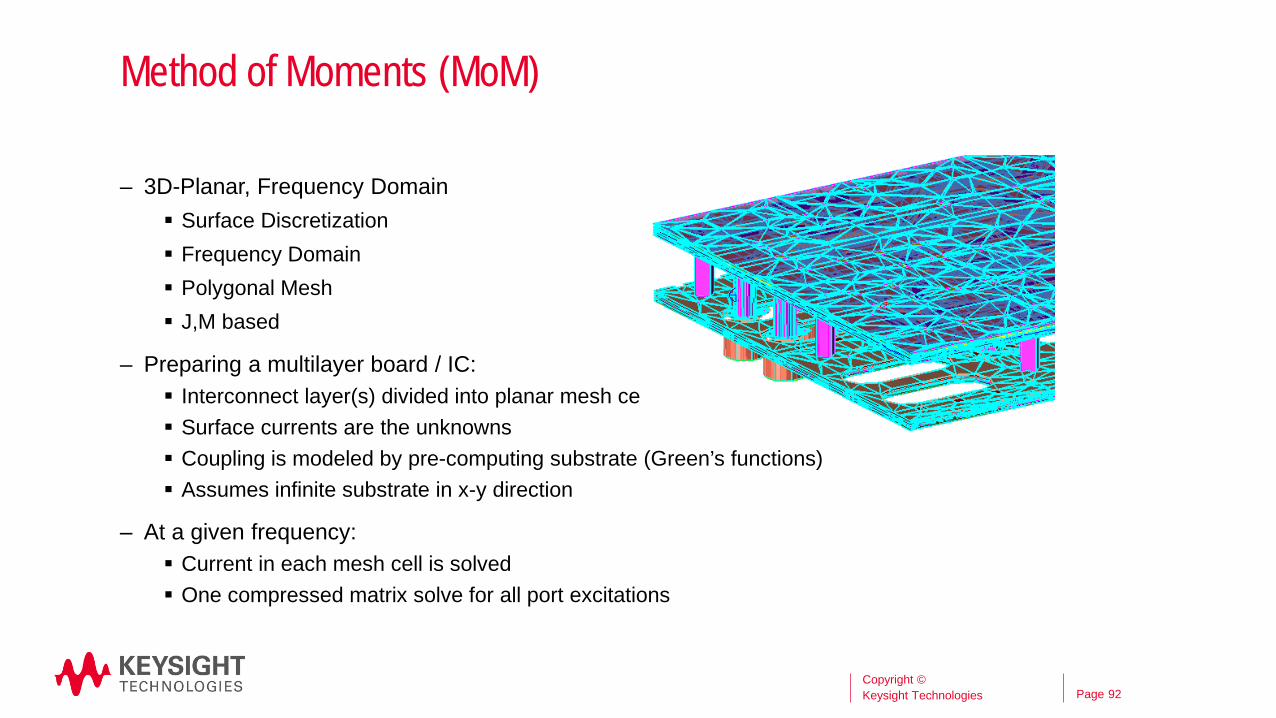
Method of Moments (MoM)
– 3D-Planar, Frequency Domain Surface Discretization Frequency Domain Polygonal Mesh J,M based
– Preparing a multilayer board / IC: Interconnect layer(s) divided into planar mesh cells Surface currents are the unknowns Coupling is modeled by pre-computing substrate (Green’s functions) Assumes infinite substrate in x-y direction
– At a given frequency: Current in each mesh cell is solved One compressed matrix solve for all port excitations
92 Copyright © Keysight Technologies
Page
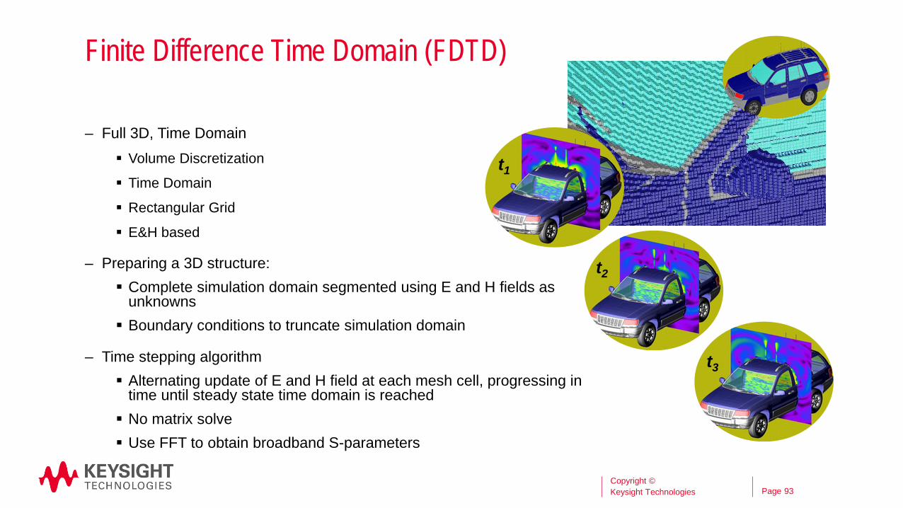
Finite Difference Time Domain (FDTD)
– Full 3D, Time Domain Volume Discretization
Time Domain
Rectangular Grid
E&H based
– Preparing a 3D structure: Complete simulation domain segmented using E and H fields as
unknowns Boundary conditions to truncate simulation domain
– Time stepping algorithm Alternating update of E and H field at each mesh cell, progressing in
time until steady state time domain is reached No matrix solve Use FFT to obtain broadband S-parameters
93
t1
t2
t3
Copyright © Keysight Technologies

Page 3/27/2015
Advanced Topics
94
– WHAT ARE EM PORTS AND PORT’S PARASITIC?
Copyright © Keysight Technologies

Page
What are EM Ports?
– An EM port is where energy is excited to the structure to calculate E&H and collect S-parameters
– Type of ports Voltage/Current Source (Internal Port in ADS)
o Not calibrated (with parasitics), but can be defined anywhere without restrictions
Sheet Ports (Edge Port in ADS) o Not calibrated , but less parasitic than Voltage Source
Waveguide Ports (Single Port in ADS) o Excites modal field/current distribution on surface o Uses Eigen-mode solver to find modes:
N modes with the highest propagation constants (N = # impedance lines)
o Inherently calibrated at all frequencies o Only available on bounding box of geometry
95 Copyright © Keysight Technologies

Page
Why Different Type of Ports and Port’s Parasitics?
– All EM ports have some parasitics: As an example, if a source is carrying current, then there is an inductance (source parasitics
inductance), which may depend on the thickness of substrate
Also if there is a change on the direction of current, it induces an inductance, which may depend on how wide the conductor is
These parasitics can be reduced by parallelizing current sources attached, which becomes a sheet port
– Port parasitics:
EMPro Workshop Version 3.0 96
I/N I Induced inductance
Waveguide Port < Sheet Port < Voltage Source
Least Most
Copyright © Keysight Technologies
Page
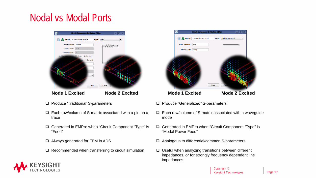
Nodal vs Modal Ports
EMPro Workshop Version 3.0 97
Node 1 Excited
Produce ‘Traditional’ S-parameters
Each row/column of S-matrix associated with a pin on a trace
Generated in EMPro when “Circuit Component “Type” is “Feed”
Always generated for FEM in ADS
Recommended when transferring to circuit simulation
Produce “Generalized” S-parameters
Each row/column of S-matrix associated with a waveguide mode
Generated in EMPro when “Circuit Component “Type” is “Modal Power Feed”
Analogous to differential/common S-parameters
Useful when analyzing transitions between different impedances, or for strongly frequency dependent line impedances
Node 2 Excited Mode 1 Excited Mode 2 Excited
Copyright © Keysight Technologies

Page
– Modal S-parameters to Nodal (or Single Ended) S-parameter conversion requires defined characteristic impedance at ports
– The port’s characteristic impedance is computed in three ways: Zpi: Power-current relationship, well defined and Momentum also uses it
Zpv: Power-voltage relationship, requires the impedance line to calculate the voltage
Zvi: Voltage-current relationship, requires the impedance line to calculate the voltage
– In TEM, these impedances become the same
Zpi, Zpv, and Zvi
98 Copyright © Keysight Technologies

Page
Impedance Lines for Waveguide Ports
– Eigenmode is modal representation
– Impedance line is to convert modal representation into nodal representation
– Z is determined by impedance line.
– Zpi (power/current) is the preferred impedance model and corresponds to Momentum
99
Z?
𝑽 = �𝑬 𝒅𝒅
Copyright © Keysight Technologies

Page
Does Port Dimension Matter?
– Yes, it is because the port boundary may interact with the structures
– Port impedance of microstrip transmission line versus the size of port dimension plot to the right proves the effect of port dimension
– 10x is a good rule-of-thumb to use
100
2
4
3
5
6
15
h w
N * h
(N+1) * w N
6 ~ 15 Range
Port impedance vs. dimension
Copyright © Keysight Technologies

Page
Does Port Dimension Matter?
– Bounded waveguide structures (coax, rectangular waveguide) Waveguide surface needs to completely ‘cover’ the guide, but minimize the
overhang
― Planar waveguide structures (microstrip, stripline, CPW)
Extend surface to the ground plane, but avoid extending beyond the ground plane
Extension to Ground Planes
101
Too Big
Too Small
About Right
Too Big
Too Small
About Right
Copyright © Keysight Technologies

Page
Does Port Dimension Matter?
– Multi-conductor lines Two ways to model multi-conductor lines in EMPro. Consider the case of two signal lines
sharing a common ground plane
Multi-conductor Lines (1)
102
One waveguide surface with multiple modes
Multiple waveguide surface with one mode per surface
Copyright © Keysight Technologies

Page
Does Port Dimension Matter? Multi-conductor lines (2)
103
+ Best accuracy, especially for tightly coupled lines
- Possible numerical issues at low frequencies
Constructed by default before ADS2012
+ Best stability at low frequencies
- Extra parasitic if surface truncates too close to the signal line
Adjacent surfaces can not overlap (they can share a common edge)
Constructed by default in ADS2012 Copyright © Keysight Technologies

Page
Why Are the Ground Reference Also Important?
Different ground reference can produce different results!
104
Ground reference is the elevated finite ground
Ground reference is the bottom infinite ground
Includes extra loading of vias, etc.
Signal
Finite Ground
Via
Infinite Ground
DUT DUT
Copyright © Keysight Technologies

Page 3/27/2015
Advanced Topics
105
– HOW DOES FEM MESHING WORK?
Copyright © Keysight Technologies

Page
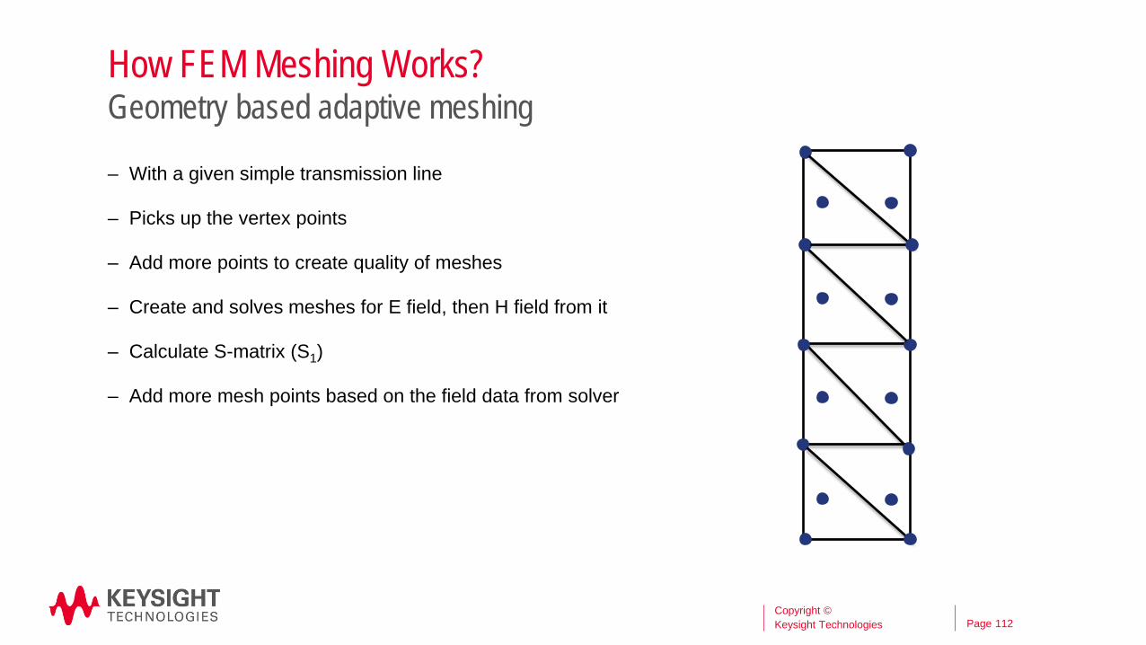
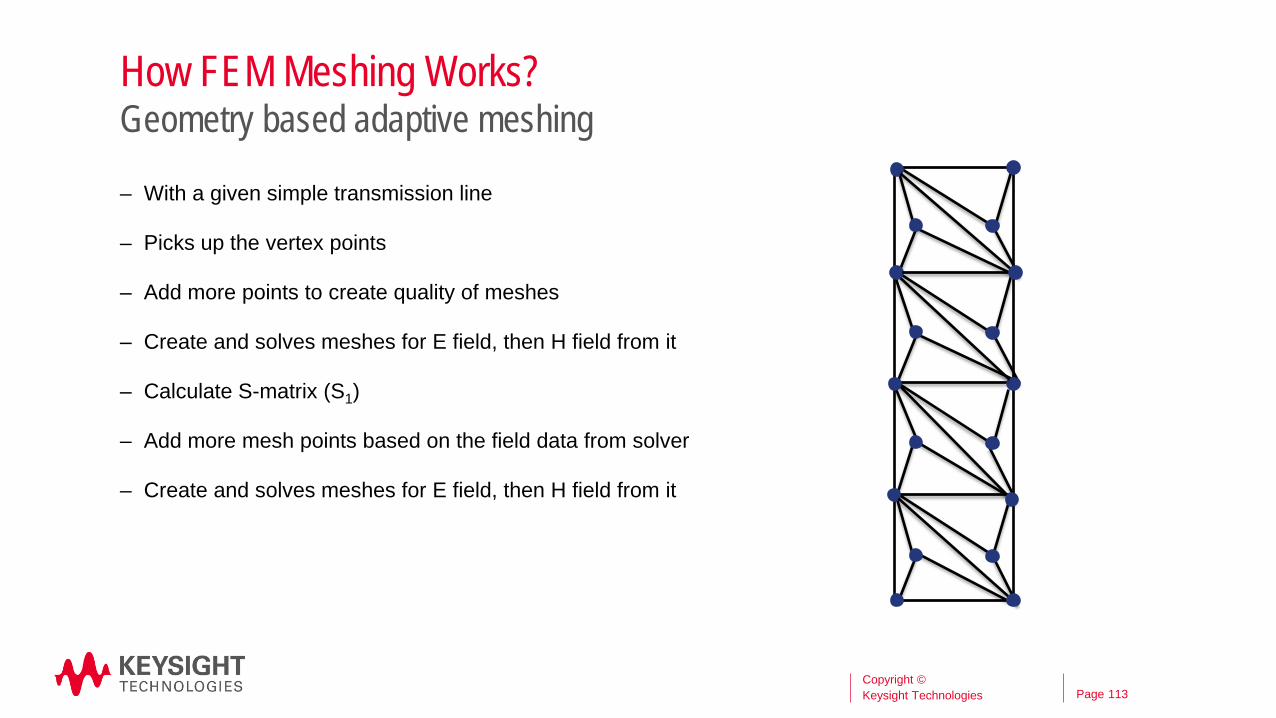
How FEM Meshing Works? Geometry based adaptive meshing
106 Copyright © Keysight Technologies

Page
How FEM Meshing Works?
– With a given simple transmission line
Geometry based adaptive meshing
107 Copyright © Keysight Technologies

Page
– With a given simple transmission line
– Picks up the vertex points
108
How FEM Meshing Works? Geometry based adaptive meshing
Copyright © Keysight Technologies

Page
How FEM Meshing Works?
– With a given simple transmission line
– Picks up the vertex points
– Add more points to create quality of meshes
Geometry based adaptive meshing
109 Copyright © Keysight Technologies

Page
How FEM Meshing Works?
– With a given simple transmission line
– Picks up the vertex points
– Add more points to create quality of meshes
– Create and solves meshes for E field, then H field from it
Geometry based adaptive meshing
110 Copyright © Keysight Technologies

Page
How FEM Meshing Works?
– With a given simple transmission line
– Picks up the vertex points
– Add more points to create quality of meshes
– Create and solves meshes for E field, then H field from it
– Calculate S-matrix (S1)
Geometry based adaptive meshing
111 Copyright © Keysight Technologies
Page
How FEM Meshing Works?
– With a given simple transmission line
– Picks up the vertex points
– Add more points to create quality of meshes
– Create and solves meshes for E field, then H field from it
– Calculate S-matrix (S1)
– Add more mesh points based on the field data from solver
Geometry based adaptive meshing
112 Copyright © Keysight Technologies
Page
How FEM Meshing Works?
– With a given simple transmission line
– Picks up the vertex points
– Add more points to create quality of meshes
– Create and solves meshes for E field, then H field from it
– Calculate S-matrix (S1)
– Add more mesh points based on the field data from solver
– Create and solves meshes for E field, then H field from it
Geometry based adaptive meshing
113 Copyright © Keysight Technologies

Page
How FEM Meshing Works?
– With a given simple transmission line
– Picks up the vertex points
– Add more points to create quality of meshes
– Create and solves meshes for E field, then H field from it
– Calculate S-matrix (S1)
– Add more mesh points based on the field data from solver
– Create and solves meshes for E field, then H field from it
– Calculate a new S-matrix (S2)
Geometry based adaptive meshing
114 Copyright © Keysight Technologies

Page
How FEM Meshing Works?
– With a given simple transmission line
– Picks up the vertex points
– Add more points to create quality of meshes
– Create and solves meshes for E field, then H field from it
– Calculate S-matrix (S1)
– Add more mesh points based on the field data from solver
– Create and solves meshes for E field, then H field from it
– Calculate a new S-matrix (S2)
– Compare S1 and S2 (S2 – S1)
Geometry based adaptive meshing
115 Copyright © Keysight Technologies

Page
How FEM Meshing Works?
– With a given simple transmission line
– Picks up the vertex points
– Add more points to create quality of meshes
– Create and solves meshes for E field, then H field from it
– Calculate S-matrix (S1)
– Add more mesh points based on the field data from solver
– Create and solves meshes for E field, then H field from it
– Calculate a new S-matrix (S2)
– Compare S1 and S2 (S2 – S1)
– Repeat the process until the difference (Sn – Sn-1) reaches to the specified Delta-S
Geometry based adaptive meshing
116 Copyright © Keysight Technologies

Page 3/27/2015
Advanced Topics
117
– FEM SURFACE/EDGE/VERTEX MESHING
Copyright © Keysight Technologies

Page
Surface/Edge/Vertex Meshing Option
– Special FEM meshing option for EMPro, only on conductor materials
– Seeds more meshes on vertices, edges, and surfaces
– Reduces the number of iterations for adaptive meshing and produce quality meshes
118
Standard Meshing Edge Meshing
Copyright © Keysight Technologies

Page
Surface/Edge/Vertex Meshing Option
– Surface/Edge/Vertex Meshing Setup It can be setup from a object(s) or part(s) level
From a part(s) from “Project Tree” , use “Grid / Meshing / Meshing Properties” menu
It can be also setup as global automatic conductor meshing
From FEM simulation setup window, use "Mesh/Refinement Properties / Initial Meshes”
119 Copyright © Keysight Technologies

Page 3/27/2015
Advanced Topics
120
– HOW DOES FDTD MESHING WORK?
Copyright © Keysight Technologies

Page
How FDTD Meshing Works? Grid based meshing
121 Copyright © Keysight Technologies

Page
How FDTD Meshing Works?
– With a given simple transmission line
Grid based meshing
122 Copyright © Keysight Technologies

Page
How FDTD Meshing Works?
– With a given simple transmission line
– Map the geometry to the closest grid lines (dashed)
Grid based meshing
123 Copyright © Keysight Technologies

Page
How FDTD Meshing Works?
– With a given simple transmission line
– Map the geometry to the closest grid lines (dashed), which then becomes meshes (green color)
Grid based meshing
124 Copyright © Keysight Technologies

Page
How FDTD Meshing Works?
– With a given simple transmission line
– Map the geometry to the closest grid lines (dashed), which then becomes meshes (green color)
– But the size is not exactly correct as shown in the picture
Grid based meshing
125 Copyright © Keysight Technologies

Page
How FDTD Meshing Works?
– With a given simple transmission line
– Map the geometry to the closest grid lines (dashed), which then becomes meshes (green color)
– But the size is not exactly correct as shown in the picture
– Fixed points help to align the meshes to the objects by adding new grid lines to the simulation domain
Grid based meshing
126 Copyright © Keysight Technologies

Page
How FDTD Meshing Works?
– With a given simple transmission line
– Map the geometry to the closest grid lines (dashed), which now becomes meshes (green color)
– But the size is not exactly correct as shown in the picture
– Fixed points help to align the meshes to the objects by adding new grid lines to the simulation domain
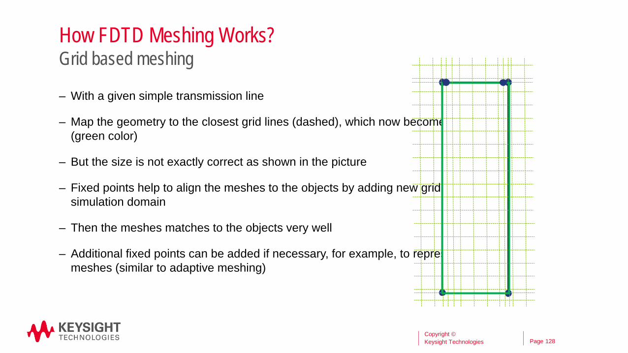
– Then the meshes matches to the objects very well
Grid based meshing
127
Meshes
Copyright © Keysight Technologies
Page
How FDTD Meshing Works?
– With a given simple transmission line
– Map the geometry to the closest grid lines (dashed), which now becomes meshes (green color)
– But the size is not exactly correct as shown in the picture
– Fixed points help to align the meshes to the objects by adding new grid lines to the simulation domain
– Then the meshes matches to the objects very well
– Additional fixed points can be added if necessary, for example, to represent edge meshes (similar to adaptive meshing)
Grid based meshing
128 Copyright © Keysight Technologies

Page
How FDTD Meshing Works?
– With a given simple transmission line
– Map the geometry to the closest grid lines (dashed), which now becomes meshes (green color)
– But the size is not exactly correct as shown in the picture
– Fixed points help to align the meshes to the objects by adding new grid lines to the simulation domain
– Then the meshes matches to the objects very well
– Additional fixed points can be added if necessary, for example, to represent edge meshes (similar to adaptive meshing)
– Grid region can be also used to mesh the structure more effectively ( x=0.5 mm for example ) to add more meshes around the area
Grid based meshing
129 Copyright © Keysight Technologies

Page 3/27/2015
Advanced Topics
130
– FDTD CONFORMAL MESHING
Copyright © Keysight Technologies

Page
FDTD Traditional Meshing
– Traditional FDTD meshes are based on “Yee” cells and they are orthogonal meshes
– For some non-orthogonal shapes or structures, it may produce very dense meshes to get quality meshes
– As a result, it may take longer to simulate and more memory to run
131
Non-Orthogonal Shapes Coarse Meshes Very Fine Meshes
Short Circuit Too Much
Copyright © Keysight Technologies
Page
FDTD Conformal Meshing
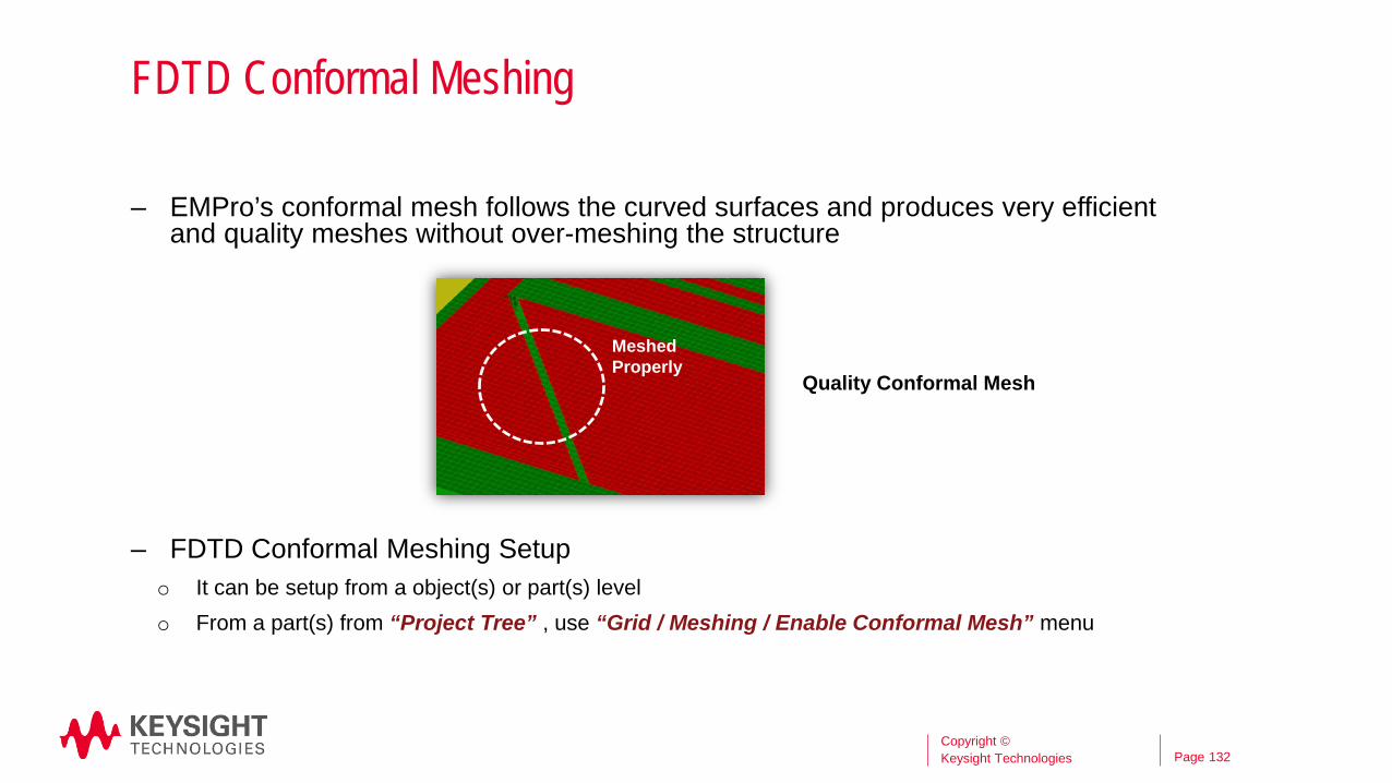
– EMPro’s conformal mesh follows the curved surfaces and produces very efficient and quality meshes without over-meshing the structure
– FDTD Conformal Meshing Setup o It can be setup from a object(s) or part(s) level o From a part(s) from “Project Tree” , use “Grid / Meshing / Enable Conformal Mesh” menu
132
Quality Conformal Mesh
Meshed Properly
Copyright © Keysight Technologies

Page 3/27/2015
Advanced Topics
133
– BOUNDING BOX AND BOUNDARY CONDITION
Copyright © Keysight Technologies
Page
Bounding Box (BBox) and Boundary Condition
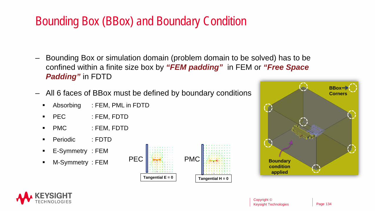
– Bounding Box or simulation domain (problem domain to be solved) has to be confined within a finite size box by “FEM padding” in FEM or “Free Space Padding” in FDTD
– All 6 faces of BBox must be defined by boundary conditions Absorbing : FEM, PML in FDTD
PEC : FEM, FDTD
PMC : FEM, FDTD
Periodic : FDTD
E-Symmetry : FEM
M-Symmetry : FEM
134
BBox Corners
Boundary condition applied
Tangential E = 0
PEC PMC
Tangential H = 0
Copyright © Keysight Technologies

Page
Symmetry Boundary Conditions
– E & M-Symmetry:
o Problem is mirrored over boundary
o Mathematical boundary condition is equivalent to PEC or PMC.
o Only need to model half of the problem: • Computationally beneficial for symmetric problems. • Sources at boundaries are taken into account. • Far field patterns are correctly computed. • Beware of excitation of modes: only even modes are part of the solution for E-Symmetry!
(MSymmetry = only odd)
135 Copyright © Keysight Technologies
Page 3/27/2015
Advanced Topics
136
– EM SOLVERS AND BASIS FUNCTIONS
Copyright © Keysight Technologies

Page
Solve Process
137
FEM MoM FDTD
Spatial Domain Full 3D 3D Layered Full 3D
Domain Frequency Frequency Time
Mesh Adaptive Fixed Fixed
Solve Technique System Solve System Solve Time Stepping
Initial Mesh
Solve @ f
Error Estimation
@ f
Mesh Refinement
Adaptive Frequency
Sweep
Discretize @ f
Pass n
Converged?
Initial Mesh
Substrate Solve @ f
Adaptive Frequency
Sweep
MOM
FEM
• Adaptive Mesh Refinement stops when convergence is detected.
• Convergence is based on delta S = ΔS, where ΔS = the largest value of the absolute difference between the S-parameters from one pass compared to the previous one.
• Determines: o Directly the expected accuracy of the S-parameter
results: o Delta S = 0.02 expected accuracy on S of
o Indirectly the expected accuracy of the circuit quantities in a bilinear way:
Pass 1
Copyright © Keysight Technologies
Page
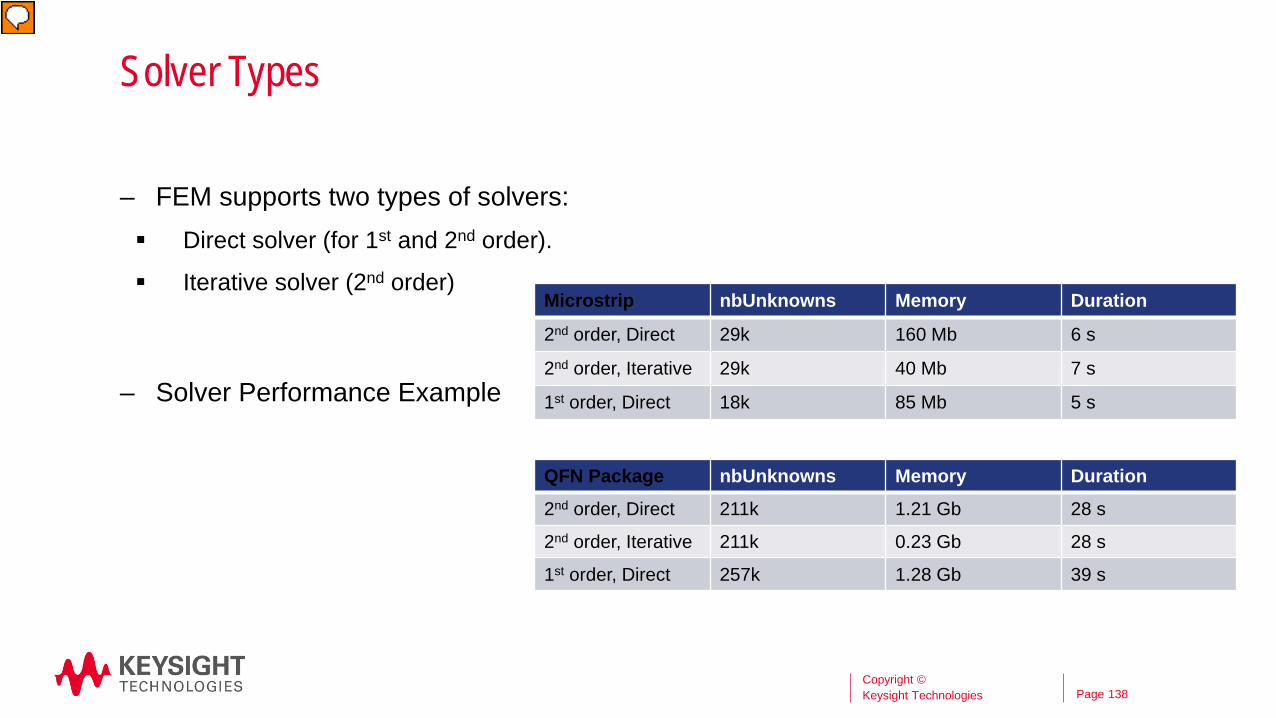
Solver Types
– FEM supports two types of solvers: Direct solver (for 1st and 2nd order).
Iterative solver (2nd order)
– Solver Performance Example
138
Microstrip nbUnknowns Memory Duration
2nd order, Direct 29k 160 Mb 6 s
2nd order, Iterative 29k 40 Mb 7 s
1st order, Direct 18k 85 Mb 5 s
QFN Package nbUnknowns Memory Duration
2nd order, Direct 211k 1.21 Gb 28 s
2nd order, Iterative 211k 0.23 Gb 28 s
1st order, Direct 257k 1.28 Gb 39 s
Copyright © Keysight Technologies

Page
Basis Functions
– Mathematical method to approximate the field values at edges and faces
• vertices and 0th order: Not used 1st order: 1 DoF per edge of a tetrahedron, resulting in 6 DoF per tetrahedron 2nd order: 2 DoF per edge, 2 DoF per face of a tetrahedron, resulting in 20 DoF per tetrahedron
• 1st – 2nd order trade-off 1st order is less efficient in approximating smooth field variations but use less memory 2nd order is less efficient for anisotropic varying fields
139
0-th order 1-st order 2-nd order
Copyright © Keysight Technologies
Page
Useful Links
– EMPro Homepage • http://www.keysight.com/en/pc-1297143/empro-3d-em-simulation-software?nid=-
34278.0.00&cc=US&lc=eng
– EMPro Application Center • http://edadocs.software.keysight.com/display/eesofapps/EM+Applications
– EMPro Forum • http://www.keysight.com/owc_discussions/forum.jspa?forumID=111
140 Copyright © Keysight Technologies