Embed Size (px)
Citation preview

Embedded Systems in SiliconTD5102
MIPS designDatapath and Control
Henk Corporaalhttp://www.ics.ele.tue.nl/~heco/courses/EmbSystems
Technical University Eindhoven
DTI / NUS Singapore
2005/2006

HC TD5102 2
Topics
Building a datapath support a subset of the MIPS-I instruction-set
A single cycle processor datapath all instruction actions in one (long) cycle
A multi-cycle processor datapath each instructions takes multiple (shorter) cycles
Exception support
HC TD5102 3
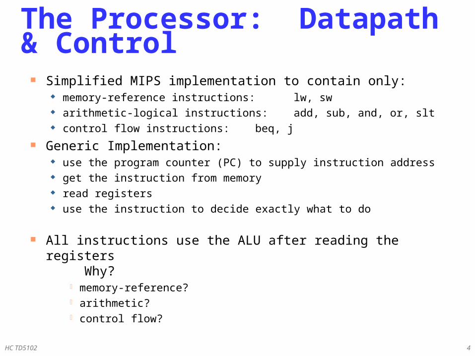
Datapath and Control
DatapathControl
Registers &Memories
Multiplexors
Buses
ALUs
FSMor
Micro-programming
HC TD5102 4
Simplified MIPS implementation to contain only: memory-reference instructions: lw, sw arithmetic-logical instructions: add, sub, and, or, slt control flow instructions: beq, j
Generic Implementation: use the program counter (PC) to supply instruction address get the instruction from memory read registers use the instruction to decide exactly what to do
All instructions use the ALU after reading the registersWhy?
memory-reference? arithmetic? control flow?
The Processor: Datapath & Control

HC TD5102 5
Abstract / Simplified View:
Two types of functional units: elements that operate on data values (combinational) elements that contain state (sequential)
More Implementation Details
Registers
Register #
Data
Register #
Datamemory
Address
Data
Register #
PC Instruction ALU
Instructionmemory
Address

HC TD5102 6
Unclocked vs. Clocked Clocks used in synchronous logic
when should an element that contains state be updated?
cycle time
rising edge
falling edge
State Elements

HC TD5102 7
The set-reset (SR) latch output depends on present inputs and also on past inputs
An unclocked state element
R
S
Q
Q
Truth table:R S Q0 0 Q0 1 11 0 01 1 ?
state change

HC TD5102 8
Output is equal to the stored value inside the element(don't need to ask for permission to look at the value)
Change of state (value) is based on the clock Latches: whenever the inputs change, and the clock is
asserted Flip-flop: state changes only on a clock edge
(edge-triggered methodology)
A clocking methodology defines when signals can be read and written— wouldn't want to read a signal at the same time it was being written
Latches and Flip-flops

HC TD5102 9
Two inputs: the data value to be stored (D) the clock signal (C) indicating when to read & store D
Two outputs: the value of the internal state (Q) and it's complement
D-latch
Q
C
D
_Q
D
C
Q

HC TD5102 10
D flip-flop
Output changes only on the clock edge
_Q
Q
_Q
Dlatch
D
C
Dlatch
DD
C
C
D
C
Q
HC TD5102 11
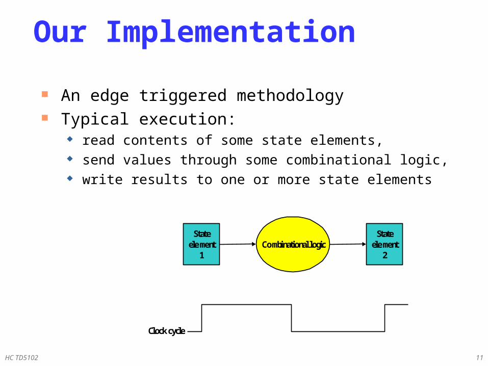
Our Implementation
An edge triggered methodology Typical execution:
read contents of some state elements, send values through some combinational logic, write results to one or more state elements
Clock cycle
Stateelement
1Combinational logic
Stateelement
2
HC TD5102 12
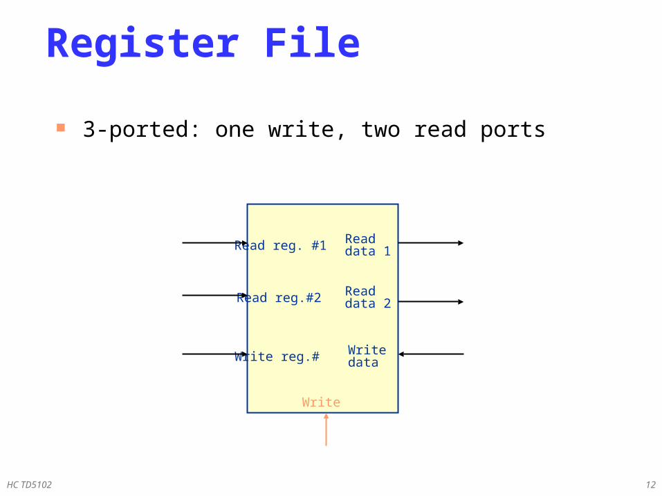
3-ported: one write, two read ports
Register File
Read reg. #1
Read reg.#2
Write reg.#
Readdata 1
Readdata 2
Write
Writedata
HC TD5102 13
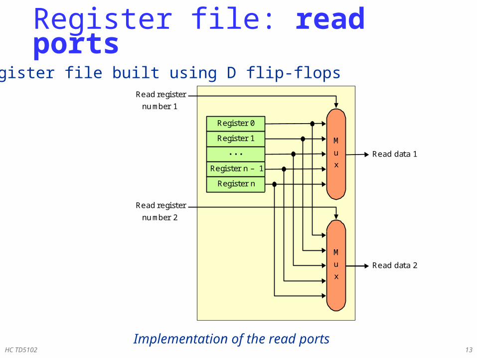
Register file: read ports
M
u
x
Register 0
Register 1
Register n – 1
Register n
M
u
xRead data 1
Read data 2
Read register
number 1
Read register
number 2
Implementation of the read ports
• Register file built using D flip-flops

HC TD5102 14
Register file: write port Note: we still use the real clock to determine when to
write
n -to -1
deco der
R eg iste r 0
R eg iste r 1
R eg is te r n – 1
C
C
D
D
R e giste r n
C
C
D
D
R eg is te r n um ber
W r ite
R e gister d ata
0
1
n – 1
n

HC TD5102 15
Simple Implementation Include the functional units we need for each instruction
Why do we need this stuff?
PC
Instructionmemory
Instructionaddress
Instruction
a. Instruction memory b. Program counter
Add Sum
c. Adder
ALU control
RegWrite
RegistersWriteregister
Readdata 1
Readdata 2
Readregister 1
Readregister 2
Writedata
ALUresult
ALU
Data
Data
Registernumbers
a. Registers b. ALU
Zero5
5
5 3
16 32Sign
extend
b. Sign-extension unit
MemRead
MemWrite
Datamemory
Writedata
Readdata
a. Data memory unit
Address

HC TD5102 16
Building the Datapath Use multiplexors to stitch them together
PC
Instructionmemory
Readaddress
Instruction
16 32
Add ALUresult
Mux
Registers
Writeregister
Writedata
Readdata 1
Readdata 2
Readregister 1Readregister 2
Shiftleft 2
4
Mux
ALU operation3
RegWrite
MemRead
MemWrite
PCSrc
ALUSrc
MemtoReg
ALUresult
ZeroALU
Datamemory
Address
Writedata
Readdata M
ux
Signextend
Add

HC TD5102 17
All of the logic is combinational
We wait for everything to settle down, and the right
thing to be done ALU might not produce “right answer” right away
we use write signals along with clock to determine when to
write
Cycle time determined by length of the longest path
Our Simple Control Structure
We are ignoring some details like setup and hold times !
Clock cycle
Stateelement
1Combinational logic
Stateelement
2
HC TD5102 18
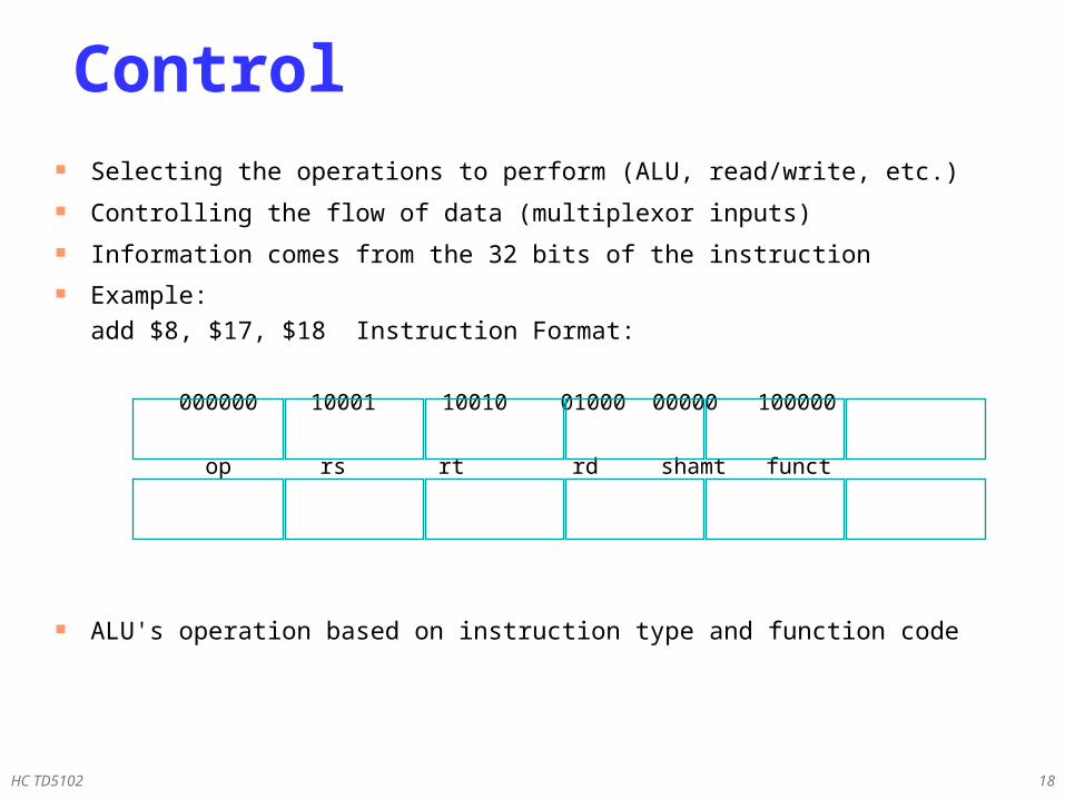
Control Selecting the operations to perform (ALU, read/write, etc.)
Controlling the flow of data (multiplexor inputs)
Information comes from the 32 bits of the instruction Example:
add $8, $17, $18 Instruction Format:
000000 10001 10010 01000 00000 100000
op rs rt rd shamt funct
ALU's operation based on instruction type and function code

HC TD5102 19
Control: 2 level implementationin
stru
ctio
n r
egis
ter ALUop
ALUcontrol
Opc
ode
Fun
ct.
31
26
0
5
bit
Control 1
Control 2
ALU
00: lw, sw01: beq10: add, sub, and, or, slt
000: and001: or010: add110: sub111: set on less than
6
6
2
3

HC TD5102 20
Datapath with Control
PC
Instructionmemory
Readaddress
Instruction[31–0]
Instruction [20–16]
Instruction [25–21]
Add
Instruction [5–0]
MemtoReg
ALUOp
MemWrite
RegWrite
MemRead
BranchRegDst
ALUSrc
Instruction [31–26]
4
16 32Instruction [15–0]
0
0Mux
0
1
Control
Add ALUresult
Mux
0
1
RegistersWriteregister
Writedata
Readdata 1
Readdata 2
Readregister 1
Readregister 2
Signextend
Shiftleft 2
Mux1
ALUresult
Zero
Datamemory
Writedata
Readdata
Mux
1
Instruction [15–11]
ALUcontrol
ALUAddress

HC TD5102 21
What should the ALU do with this instructionexample: lw $1, 100($2)
35 2 1 100
op rs rt 16 bit offset
ALU control input
000 AND001 OR010 add110 subtract111 set-on-less-than
Why is the code for subtract 110 and not 011?
ALU Control1

HC TD5102 22
Must describe hardware to compute 3-bit ALU control input given instruction type
00 = lw, sw01 = beq, 10 = arithmetic
function code for arithmetic Describe it using a truth table (can turn into gates):
ALU Operation class, computed from instruction type
ALU Control1
ALUOp Funct field OperationALUOp1 ALUOp0 F5 F4 F3 F2 F1 F0
0 0 X X X X X X 010X 1 X X X X X X 1101 X X X 0 0 0 0 0101 X X X 0 0 1 0 1101 X X X 0 1 0 0 0001 X X X 0 1 0 1 0011 X X X 1 0 1 0 111
outputsintputs

HC TD5102 23
ALU Control1
Simple combinational logic (truth tables)
Operation2
Operation1
Operation0
Operation
ALUOp1
F3
F2
F1
F0
F (5– 0)
ALUOp0
ALUOp
ALU control block

HC TD5102 24
Deriving Control2 signals
Instruction RegDst ALUSrcMemto-
RegReg
WriteMem Read
Mem Write Branch ALUOp1 ALUp0
R-format 1 0 0 1 0 0 0 1 0lw 0 1 1 1 1 0 0 0 0sw X 1 X 0 0 1 0 0 0beq X 0 X 0 0 0 1 0 1
9 control (output) signals
Determine these control signals directly from the opcodes:R-format: 0lw: 35sw: 43beq: 4
Input6-bits

HC TD5102 25
Control 2
PLA example implementation
R-format Iw sw beq
Op0
Op1
Op2
Op3
Op4
Op5
Inputs
Outputs
RegDst
ALUSrc
MemtoReg
RegWrite
MemRead
MemWrite
Branch
ALUOp1
ALUOpO
HC TD5102 26
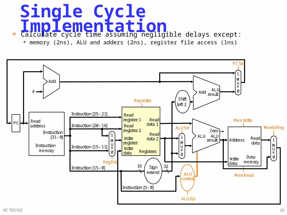
Single Cycle Implementation Calculate cycle time assuming negligible delays except:
memory (2ns), ALU and adders (2ns), register file access (1ns)
MemtoReg
MemRead
MemWrite
ALUOp
ALUSrc
RegDst
PC
Instructionmemory
Readaddress
Instruction[31– 0]
Instruction [20– 16]
Instruction [25– 21]
Add
Instruction [5– 0]
RegWrite
4
16 32Instruction [15– 0]
0Registers
WriteregisterWritedata
Writedata
Readdata 1
Readdata 2
Readregister 1Readregister 2
Signextend
ALUresult
Zero
Datamemory
Address Readdata
Mux
1
0
Mux
1
0
Mux
1
0
Mux
1
Instruction [15– 11]
ALUcontrol
Shiftleft 2
PCSrc
ALU
Add ALUresult

HC TD5102 27
Single Cycle Implementation
Memory (2ns), ALU & adders (2ns), reg. file access (1ns)
Fixed length clock: longest instruction is the ‘lw’ which requires 8 ns
Variable clock length (not realistic, just as exercise): R-instr: 6 ns Load: 8 ns Store: 7 ns Branch: 5 ns Jump: 2 ns
Average depends on instruction mix (see pg 374)

HC TD5102 28
Where we are headed Single Cycle Problems:
what if we had a more complicated instruction like floating point? wasteful of area: NO Sharing of Hardware resources
One Solution: use a “smaller” cycle time have different instructions take different numbers of cycles a “multicycle” datapath:
PC
Memory
Address
Instructionor data
Data
Instructionregister
Registers
Register #
Data
Register #
Register #
ALU
Memorydata
register
A
B
ALUOut
IR
MDR
HC TD5102 29
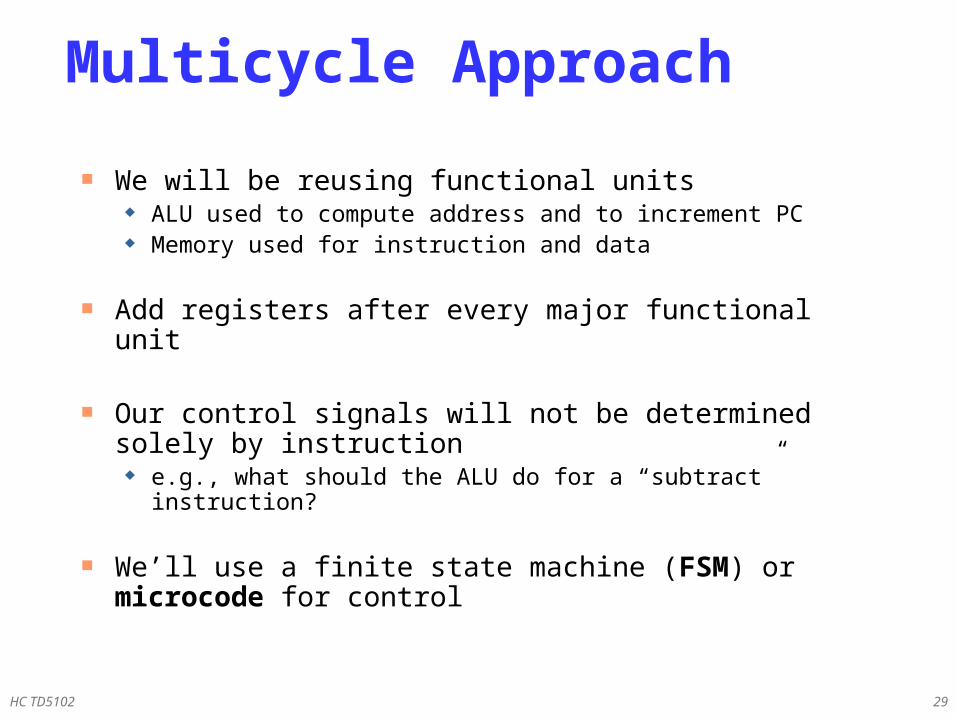
We will be reusing functional units ALU used to compute address and to increment PC Memory used for instruction and data
Add registers after every major functional unit
Our control signals will not be determined solely by instruction e.g., what should the ALU do for a “subtract” instruction?
We’ll use a finite state machine (FSM) or microcode for control
Multicycle Approach
HC TD5102 30
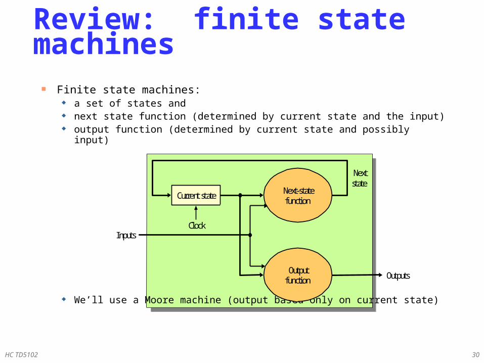
Finite state machines: a set of states and next state function (determined by current state and the input) output function (determined by current state and possibly input)
We’ll use a Moore machine (output based only on current state)
Review: finite state machines
Next-statefunction
Current state
Clock
Outputfunction
Nextstate
Outputs
Inputs

HC TD5102 31
Break up the instructions into steps, each step takes a cycle balance the amount of work to be done restrict each cycle to use only one major functional unit
At the end of a cycle store values for use in later cycles (easiest thing to do) introduce additional “internal” registers
Notice: we distinguish processor state: programmer visible registers internal state: programmer invisible registers (like IR, MDR,
A, B, and ALUout)
Multicycle Approach

HC TD5102 32
Multicycle Approach
Shiftleft 2
PC
Memory
MemData
Writedata
Mux
0
1
RegistersWriteregister
Writedata
Readdata 1
Readdata 2
Readregister 1
Readregister 2
Mux
0
1
Mux
0
1
4
Instruction[15–0]
Signextend
3216
Instruction[25–21]
Instruction[20–16]
Instruction[15–0]
Instructionregister
1 Mux
0
3
2
Mux
ALUresult
ALUZero
Memorydata
register
Instruction[15–11]
A
B
ALUOut
0
1
Address

HC TD5102 33
Multicycle Approach Note that previous picture does not include:
branch support jump support Control lines and logic
Tclock > max (ALU delay, Memory access, Regfile access)
See book for complete picture
HC TD5102 34
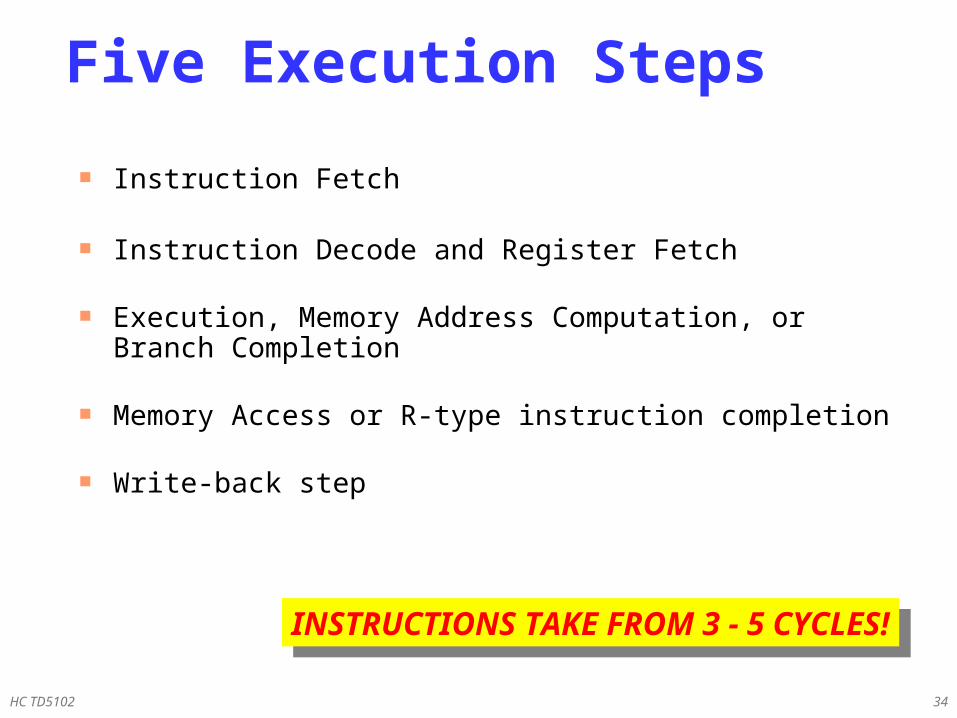
Instruction Fetch
Instruction Decode and Register Fetch
Execution, Memory Address Computation, or Branch Completion
Memory Access or R-type instruction completion
Write-back step
Five Execution Steps
INSTRUCTIONS TAKE FROM 3 - 5 CYCLES!INSTRUCTIONS TAKE FROM 3 - 5 CYCLES!

HC TD5102 35
Use PC to get instruction and put it in the Instruction Register
Increment the PC by 4 and put the result back in the PC Can be described succinctly using RTL "Register-Transfer
Language"
IR = Memory[PC];PC = PC + 4;
Can we figure out the values of the control signals?
What is the advantage of updating the PC now?
Step 1: Instruction Fetch

HC TD5102 36
Read registers rs and rt in case we need them Compute the branch address in case the instruction is a
branch Previous two actions are done optimistically!! RTL:
A = Reg[IR[25-21]]; B = Reg[IR[20-16]]; ALUOut = PC+(sign-extend(IR[15-0])<< 2);
We aren't setting any control lines based on the instruction type
(we are busy "decoding" it in our control logic)
Step 2: Instruction Decode and Register Fetch
HC TD5102 37
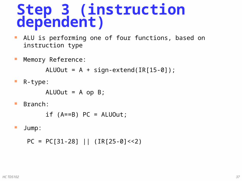
ALU is performing one of four functions, based on instruction type
Memory Reference:
ALUOut = A + sign-extend(IR[15-0]);
R-type:
ALUOut = A op B;
Branch:
if (A==B) PC = ALUOut;
Jump:
PC = PC[31-28] || (IR[25-0]<<2)
Step 3 (instruction dependent)

HC TD5102 38
Loads and stores access memory
MDR = Memory[ALUOut];or
Memory[ALUOut] = B;
R-type instructions finish
Reg[IR[15-11]] = ALUOut;
The write actually takes place at the end of the cycle on the edge
Step 4 (R-type or memory-access)

HC TD5102 39
Memory read completion step
Reg[IR[20-16]]= MDR;
What about all the other instructions?
Write-back step

HC TD5102 40
Step nameAction for R-type
instructionsAction for memory-reference
instructionsAction for branches
Action for jumps
Instruction fetch IR = Memory[PC]PC = PC + 4
Instruction A = Reg [IR[25-21]]decode/register fetch B = Reg [IR[20-16]]
ALUOut = PC + (sign-extend (IR[15-0]) << 2)
Execution, address ALUOut = A op B ALUOut = A + sign-extend if (A ==B) then PC = PC [31-28] IIcomputation, branch/ (IR[15-0]) PC = ALUOut (IR[25-0]<<2)jump completion
Memory access or R-type Reg [IR[15-11]] = Load: MDR = Memory[ALUOut]completion ALUOut or
Store: Memory [ALUOut] = B
Memory read completion Load: Reg[IR[20-16]] = MDR
Steps taken to execute any instruction class
Summary execution steps

HC TD5102 41
How many cycles will it take to execute this code?
lw $t2, 0($t3)lw $t3, 4($t3)beq $t2, $t3, L1 #assume not takenadd $t5, $t2, $t3sw $t5, 8($t3)
L1: ...
What is going on during the 8th cycle of execution? In what cycle does the actual addition of $t2 and $t3 takes
place?
Simple Questions

HC TD5102 42
Value of control signals is dependent upon: what instruction is being executed which step is being performed
Use the information we have accumulated to specify a finite state machine (FSM) specify the finite state machine graphically, or use microprogramming
Implementation can be derived from specification
Implementing the Control

HC TD5102 43
FSM: high level view
Start/reset
Instruction fetch, decode and register fetch
Memory accessinstructions
R-type instructions
Branch instruction
Jumpinstruction

How many state bits will we need?
Graphical Specification of FSM
PCWritePCSource = 10
ALUSrcA = 1ALUSrcB = 00ALUOp = 01PCWriteCond
PCSource = 01
ALUSrcA =1ALUSrcB = 00ALUOp = 10
RegDst = 1RegWrite
MemtoReg = 0
MemWriteIorD = 1
MemReadIorD = 1
ALUSrcA = 1ALUSrcB = 10ALUOp = 00
RegDst = 0RegWrite
MemtoReg = 1
ALUSrcA = 0ALUSrcB = 11ALUOp = 00
MemReadALUSrcA = 0
IorD = 0IRWrite
ALUSrcB = 01ALUOp = 00
PCWritePCSource = 00
Instruction fetchInstruction decode/
register fetch
Jumpcompletion
BranchcompletionExecution
Memory addresscomputation
Memoryaccess
Memoryaccess R-type completion
Write-back step
(Op = 'LW') or (Op = 'SW') (Op = R-type)
(Op
= 'B
EQ')
(Op
= 'J
' )
(Op = 'SW
')
(Op
= ' L
W' )
4
01
9862
753
Start

HC TD5102 45
Implementation:
Finite State Machine for ControlPCWrite
PCWriteCond
IorD
MemtoReg
PCSource
ALUOp
ALUSrcB
ALUSrcA
RegWrite
RegDst
NS3NS2NS1NS0
Op5
Op4
Op3
Op2
Op1
Op0
S3
S2
S1
S0
State register
IRWrite
MemRead
MemWrite
Instruction registeropcode field
Outputs
Control logic
Inputs

HC TD5102 46
PLA Implemen-tation
If I picked a horizontal or vertical line could you explain it ?
What type of FSM is used?
Op5
Op4
Op3
Op2
Op1
Op0
S3
S2
S1
S0
IorD
IRWrite
MemReadMemWrite
PCWritePCWriteCond
MemtoRegPCSource1
ALUOp1
ALUSrcB0ALUSrcARegWriteRegDstNS3NS2NS1NS0
ALUSrcB1ALUOp0
PCSource0
(see fig C.14)
nextstate
currentstate
datapath control
opco
de

HC TD5102 47
ROM = "Read Only Memory" values of memory locations are fixed ahead of time
A ROM can be used to implement a truth table if the address is m-bits, we can address 2m entries in the ROM our outputs are the bits of data that the address points to
ROM Implementation
0 0 0 0 0 1 10 0 1 1 1 0 00 1 0 1 1 0 00 1 1 1 0 0 0 1 0 0 0 0 0 0 1 0 1 0 0 0 11 1 0 0 1 1 01 1 1 0 1 1 1
m is the "heigth", and n is the "width"
mbits
nbits
ROMaddress data

HC TD5102 48
How many inputs are there?6 bits for opcode, 4 bits for state = 10 address lines(i.e., 210 = 1024 different addresses)
How many outputs are there?16 datapath-control outputs, 4 state bits = 20 outputs
ROM is 210 x 20 = 20K bits (very large and a rather unusual size)
Rather wasteful, since for lots of the entries, the outputs are the same
— i.e., opcode is often ignored
ROM Implementation

HC TD5102 49
ROM Implementation
Cheaper implementation:
Exploit the fact that the FSM is a Moore machine ==> Control outputs only depend on current state and not on other
incoming control signals ! Next state depends on all inputs
Break up the table into two parts— 4 state bits tell you the 16 outputs, 24 x 16 bits of ROM— 10 bits tell you the 4 next state bits, 210 x 4 bits of ROM— Total number of bits: 4.3K bits of ROM

HC TD5102 50
PLA is much smaller can share product terms (ROM has an entry (=address) for every product
term only need entries that produce an active output can take into account don't cares
Size of PLA:(#inputs #product-terms) + (#outputs #product-terms) For this example: (10x17)+(20x17) = 460 PLA cells
PLA cells usually slightly bigger than the size of a ROM cell
ROM vs PLA
HC TD5102 51
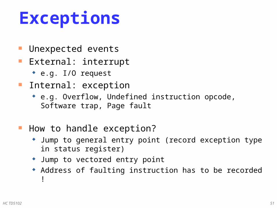
Exceptions
Unexpected events External: interrupt
e.g. I/O request Internal: exception
e.g. Overflow, Undefined instruction opcode, Software trap, Page fault
How to handle exception? Jump to general entry point (record exception type in status
register) Jump to vectored entry point Address of faulting instruction has to be recorded !

HC TD5102 52
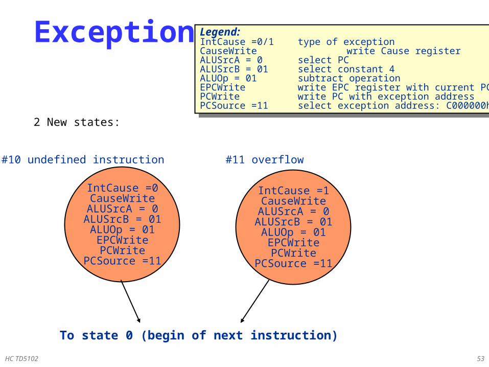
Exceptions
Changes needed: see fig. 5.48 / 5.49 / 5.50
Extend PC input mux with extra entry with fixed address: “C000000hex”
Add EPC register containing old PC (we’ll use the ALU to decrement PC with 4) extra input ALU src2 needed with fixed value 4
Cause register (one bit in our case) containing: 0: undefined instruction 1: ALU overflow
Add 2 states to FSM undefined instr. state #10 overflow state #11
HC TD5102 53
Exceptions
2 New states:
Legend:IntCause =0/1 type of exceptionCauseWrite write Cause registerALUSrcA = 0 select PCALUSrcB = 01 select constant 4ALUOp = 01 subtract operationEPCWrite write EPC register with current PCPCWrite write PC with exception addressPCSource =11 select exception address: C000000hex
Legend:IntCause =0/1 type of exceptionCauseWrite write Cause registerALUSrcA = 0 select PCALUSrcB = 01 select constant 4ALUOp = 01 subtract operationEPCWrite write EPC register with current PCPCWrite write PC with exception addressPCSource =11 select exception address: C000000hex
IntCause =0CauseWrite
ALUSrcA = 0ALUSrcB = 01ALUOp = 01
EPCWritePCWrite
PCSource =11
IntCause =1CauseWrite
ALUSrcA = 0ALUSrcB = 01ALUOp = 01
EPCWritePCWrite
PCSource =11
#10 undefined instruction #11 overflow
To state 0 (begin of next instruction)