Embed Size (px)
Citation preview

Spring 2014 S. Hoyos-ECEN-610 1
ELEN 610
Data Converters
Sebastian Hoyos
Texas A&M University
Analog and Mixed Signal Group

Spring 2014 S. Hoyos-ECEN-610 2
Folding

Spring 2014 S. Hoyos-ECEN-610 3
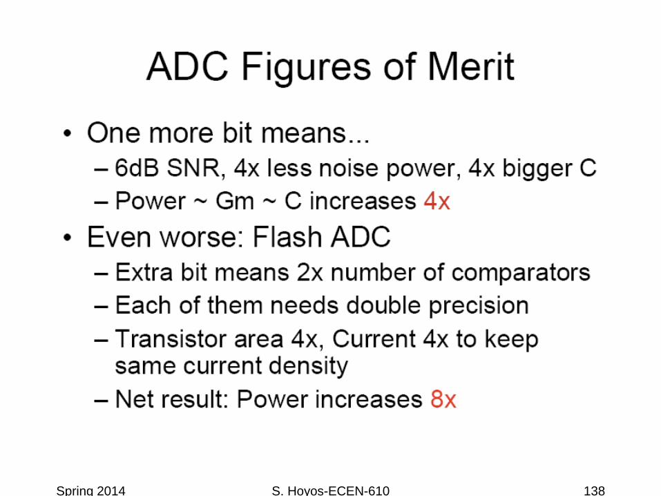
Inefficiency of Flash ADC
Only comparators in the vicinity of Vin are active at a time → low efficiency.
… …
En
co
de
r
VFS Vi
fs
Strobe
Do
2N-1
comparators
…
VFS
0
2N-1
…Vi
Do

Spring 2014 S. Hoyos-ECEN-610 4
Segmented Quantization
Analog pre-processing
divides Vin into 2M
uniformly-spaced
segments.
VFS
0
2N-1
…
Vi
Do
1 2 3 4 5 6 7 8
Segment indicator (M bits)
Fine quantization
(N-M) bits

Spring 2014 S. Hoyos-ECEN-610 5
Signal Folding
• Analog pre-processing
→ folding amplifier
• Folding factor (F) is
equal to the number of
folded segments.
Segment indicator (log2(F) bits)
Fine quantization
N-log2(F) bits
VFS
0
2N-1
…
Vi
Do
1 2 3 4 5 6 7 8
Spring 2014 S. Hoyos-ECEN-610 6
Folding ADC Architecture
• The fine ADC performs amplitude quantization on the folded signal.
• The coarse ADC differentiates which segment Vin resides in.
Dout
Re
fere
nce
La
dd
er
Coarse
ADC
Dig
ita
l L
og
ic
8 bits
3 bits
Fine ADC
5 bits
ViVR
LSB’s
MSB’s F = 8
Spring 2014 S. Hoyos-ECEN-610 7
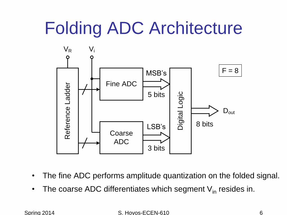
Folding Amplifier
F = 3Vo+
Vo-
Vi
M1 M2 M3 M4
RL RL
M5 M6
VR/2 5VR/6VR/6
Vi
Vo
ISRL
0
ISISIS
-ISRL
VR1
VR2
VR3

Spring 2014 S. Hoyos-ECEN-610 8
Signal Folding
Pros
• Folding reduces the comparator number by the folding factor F, and also reduces the number of preamplifiers by F but adds F folder amplifiers.
Cons
• Multiple differential pairs in the folder increases the output loading.
• “Frequency multiplication” at the folder output.

Spring 2014 S. Hoyos-ECEN-610 9
Frequency Multiplication
)2(sin 1max
F
ff in
Spring 2014 S. Hoyos-ECEN-610 10
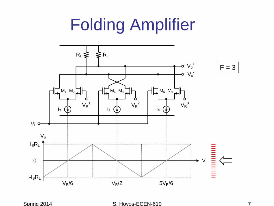
Folding Amplifier
F = 3Vo+
Vo-
Vi
M1 M2 M3 M4
RL RL
M5 M6
VR/2 5VR/6VR/6
Vi
Vo
ISRL
0
ISISIS
-ISRL
VR1
VR2
VR3
Zero-crossings
are still precise!

Spring 2014 S. Hoyos-ECEN-610 11
Zero-Crossing Detection
• Only detect zero-crossings instead of fine amplitude quantization
→ insensitive to folder nonlinearities.
• P parallel folding amplifiers are required.
F = 3, P = 4
Vi
Vo
0

Spring 2014 S. Hoyos-ECEN-610 12
Offset Parallel Folding
• Total # of zero-crossings = Total # of preamps = P*F
• Parallel folding saves the # of comparators, but not the # of preamps
→ still large Cin.
F = 3, P = 4
Re
fere
nce
La
dd
er
Folder 2 V2
Folder 1 V1
ViVR
Folder 3 V3
Folder 4 V4
Vi0
Vi0
Vi0
Vi0
c
c
c
c

Spring 2014 S. Hoyos-ECEN-610 13
Folding + Interpolation
Vi
…
Vi
…
…
Cross-connect
P & N sides at
the endpoints
c

Spring 2014 S. Hoyos-ECEN-610 14
“Rounding” Problem
• Large F results in signal “rounding”, causing gain and swing loss.
• Max. folding factor is limited by Vov of folder and supply voltage.
F = 3
F = 9
Vi0
Vi0
Vo
Vo
2√2(Vgs-Vth)
2√2(Vgs-Vth)

Spring 2014 S. Hoyos-ECEN-610 15
Folding vs. Interpolation/Averaging
Folding
• Folding works better with non-overlapped active regions between
adjacent folders.
• Large Vov (for high speed) of folders and low supply voltage limit
the max. achievable F.
Interpolation/Averaging
• Work better with closely spaced overlapped active region between
adjacent folding signals.
Observation
• Small F and large P (parallel folders) will help both folding and
interpolation/averaging, but introduces large Cin.
• What else can we do?
Spring 2014 S. Hoyos-ECEN-610 16
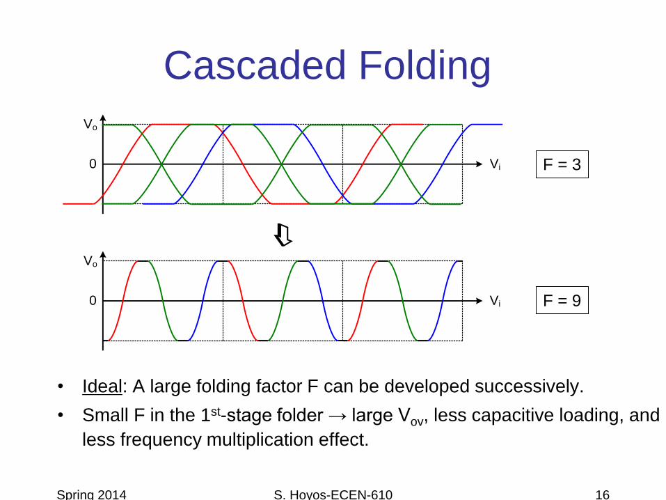
Cascaded Folding
• Ideal: A large folding factor F can be developed successively.
• Small F in the 1st-stage folder → large Vov, less capacitive loading, and
less frequency multiplication effect.
F = 3
F = 9
Vi0
Vo
Vi0
Vo
c

Spring 2014 S. Hoyos-ECEN-610 17
Cascaded Folder Architecture (I)
• Gilbert four-quadrant multiplier based folding amplifier
• Only works with even P, requires a lot of headroom
F = ?

Spring 2014 S. Hoyos-ECEN-610 18
Cascaded Folder Architecture (II)
• Simple differential pair-based folding amplifiers
• Only works with odd P, compatible with low supply voltage.
…
Vi
……
…
……
Vo+
Vo-
F = ?

Spring 2014 S. Hoyos-ECEN-610 19
Mechanical Model of Cascaded Folding
Bult (JSSC’97)

Spring 2014 S. Hoyos-ECEN-610 20
Distributed Preamplification
Large signal gain developed gradually along the signal path
→ from “soft” to “hard” decision
…
Input and Reference Ladder
1st-stage Folding and Averaging
…Interpolation and 2
nd-stage Folding
…
Interpolation and Averaging
Comparators
c
c
c
c
Gain

Spring 2014 S. Hoyos-ECEN-610 21
Cascaded Offset Bit Alignment
Two-step offset bit alignment – large offset tolerance on F1 coarse
comparators and medium tolerance on P comparators.
Dout
Re
fere
nce
La
dd
er
F1
Cm
p’s
Dig
ita
l L
og
ic
ViVR
MSB’s
LSB’s
1st -s
tag
e F
old
ers
(P
*F1)
2n
d-s
tag
e F
old
ers
(F
2)
P
Cm
p’s
Fin
e C
om
pa
rato
rs
Bit
Alignment

Spring 2014 S. Hoyos-ECEN-610 22
Useful Formulas
Assuming a two-stage cascaded folding & interpolating ADC,
F1 = 1st-stage folding factor, F2 = 2nd-stage folding factor,
P = # of offset parallel folders (P>F2), I = total interpolation factor,
then
total # of decision level = P*F1*I,
ADC Resolution = Log2(P*F1*I),
total # of preamps in 1st folder = P*F1,
total # of preamps in 2nd folder = P,
total # of fine comparators = P*I/F2,
total # of coarse comparators = F1*F2, F1+F2, or F1+P?

Spring 2014 S. Hoyos-ECEN-610 23
Cascaded Offset Bit Alignment
• F1 coarse comparators at input and P coarse comparators at 1st-stage
folder outputs resolve F1*P (>F1*F2) folds.
• One fine comparator output is utilized to perform offset bit alignment.
D
Vi
C
B
A
VFS
0
0 0 0 10 0 1 10 1 1 11 1 1 11 1 1 01 1 0 01 0 0 00 0 0 0
D C B A
0 0 0 10 0 1 10 1 1 11 1 1 11 1 1 01 1 0 01 0 0 00 0 0 0
0 0 0 0
0 0 0 0
A
Margin
1
2
3
4
5OF
UF
Spring 2014 S. Hoyos-ECEN-610 24
References1. R. J. van De Plassche et al., JSSC, vol. 14, pp. 938, issue 6, 1979.
2. R. E. J. van De Grift et al., JSSC, vol. 19, pp. 374-378, issue 3, 1984.
3. R. E. J. van De Grift et al., JSSC, vol. 22, pp. 944-953, issue 6, 1987.
4. R. J. van de Plassche et al., JSSC, vol. 23, pp. 1334-1344, issue 6, 1988.
5. J. van Valburg et al., JSSC, vol. 27, pp. 1662-1666, issue 12, 1992.
6. B. Nauta et al., JSSC, vol. 30, pp. 1302-1308, issue 12, 1995.
7. A. G. W. Venes et al., JSSC, vol. 31, pp. 1846-1853, issue 12, 1996.
8. M. P. Flynn et al., JSSC, vol. 31, pp. 1248-1257, issue 9, 1996.
9. P. Vorenkamp et al., JSSC, vol. 32, pp. 1876-1886, issue 12, 1997.
10. K. Bult et al., JSSC, vol. 32, pp. 1887-1895, issue 12, 1997.
11. M. P. Flynn et al., JSSC, vol. 33, pp. 1932-1938, issue 12, 1998.
12. M.-J. Choe et al., VLSI, 1999, pp. 81-82.
13. R. C. Taft et al., JSSC, vol. 39, pp. 2107, issue 12, 2004.
Spring 2014 S. Hoyos-ECEN-610 25
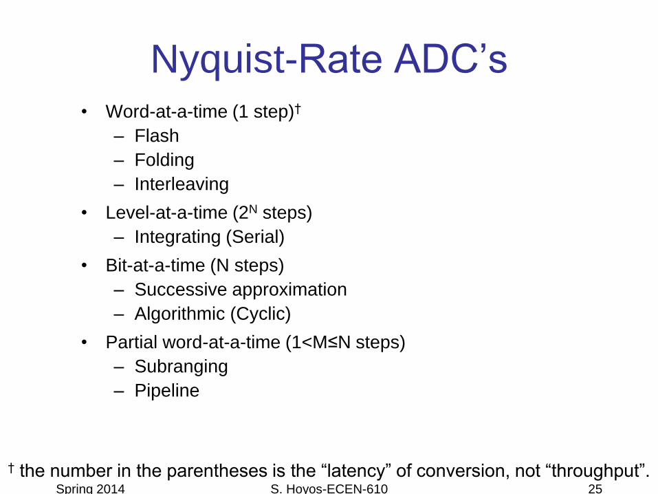
Nyquist-Rate ADC’s• Word-at-a-time (1 step)†
– Flash
– Folding
– Interleaving
• Level-at-a-time (2N steps)
– Integrating (Serial)
• Bit-at-a-time (N steps)
– Successive approximation
– Algorithmic (Cyclic)
• Partial word-at-a-time (1<M≤N steps)
– Subranging
– Pipeline
† the number in the parentheses is the “latency” of conversion, not “throughput”.
Spring 2014 S. Hoyos-ECEN-610 26
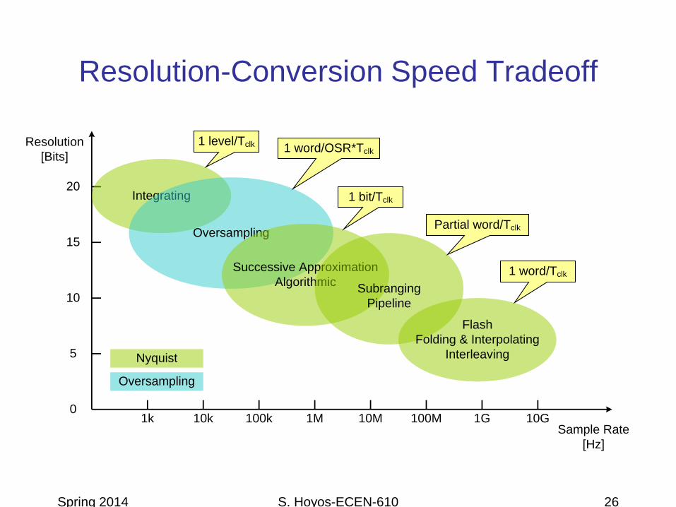
Resolution-Conversion Speed Tradeoff
0
Resolution
[Bits]
5
10
15
20
1k 10k 100k 1M 10M 100M 1G 10GSample Rate
[Hz]
Integrating
Oversampling
Successive Approximation
AlgorithmicSubranging
Pipeline
Flash
Folding & Interpolating
Interleaving
1 level/Tclk 1 word/OSR*Tclk
1 bit/Tclk
Partial word/Tclk
1 word/Tclk
Nyquist
Oversampling

Spring 2014 S. Hoyos-ECEN-610 27
Integrating ADC

Spring 2014 S. Hoyos-ECEN-610 28
Single-Slope Integrating ADC
• Counter keeps counting until comparator output toggles.
• Simple, inherently monotonic, but very slow (2N*Tclk/sample).
Vi
Control
CI
fclk Counter Do
VX
VY

Spring 2014 S. Hoyos-ECEN-610 29
Single-Slope Integrating ADC
• INL depends on the linearity of the ramp signal.
• Precision capacitor (C) and current source (I) are required.
• Comparator must handle large common-mode input.
VX
VY
t
t
t1
start stop
slope=I/C
.
, 11
i
clk
o
clk
oi
VTI
CD
T
tDt
C
IV
Spring 2014 S. Hoyos-ECEN-610 30
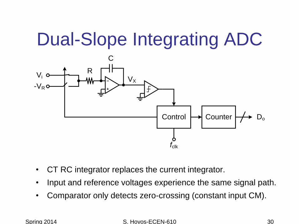
Dual-Slope Integrating ADC
• CT RC integrator replaces the current integrator.
• Input and reference voltages experience the same signal path.
• Comparator only detects zero-crossing (constant input CM).
Vi
Control
fclk
Counter Do
VX
R
C
-VR
Spring 2014 S. Hoyos-ECEN-610 31
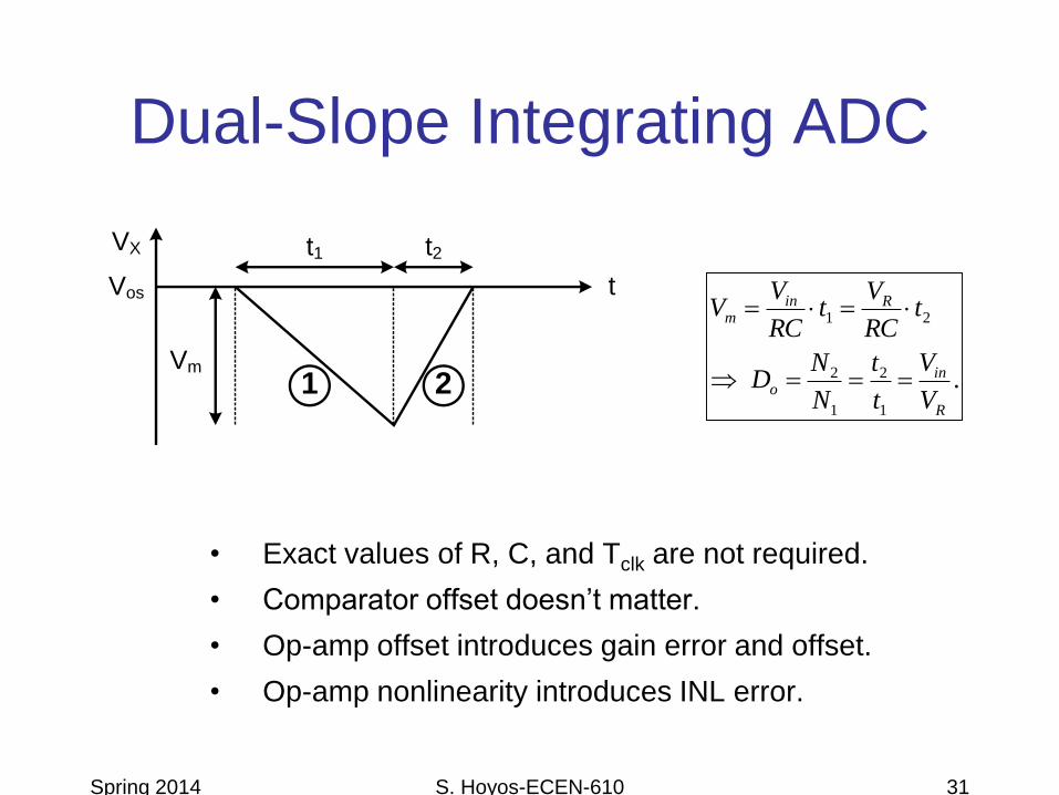
Dual-Slope Integrating ADC
• Exact values of R, C, and Tclk are not required.
• Comparator offset doesn’t matter.
• Op-amp offset introduces gain error and offset.
• Op-amp nonlinearity introduces INL error.
.1
2
1
2
21
R
ino
Rinm
V
V
t
t
N
ND
tRC
Vt
RC
VV
VX
t
t1 t2
1 2Vm
Vos

Spring 2014 S. Hoyos-ECEN-610 32
Subranging Dual-Slope ADC
• Much faster conversion speed.
• Two matched current sources and two comparators are required.
Vi
Control
Logic
SHA
Cnt 1
(8 bits) MSB’s
VX
C2
I
CS
I
256
C1
Vt
Cnt 2
(8 bits)LSB’s
fclk Carry

Spring 2014 S. Hoyos-ECEN-610 33
Subranging Dual-Slope ADC
• Precise Vt is not required if carry is propagated.
• Matching between the current sources is critical
→ if I1 = I, I2 = (1+δ)·I/256, then |δ| ≤ 0.5/256.
.
256
2
,1
C
I
dt
dV
C
I
dt
dV
X
X
VX
t
t1 t2
1 2
Vt
21 NWNDo

Spring 2014 S. Hoyos-ECEN-610 34
Subranging Multi-Slope ADC
Vi
Control
Logic
SHA
Cnt 2 4 Bits
VX
I
CS
I
256
Cnt 3 4 BitsI
16
Cnt 1 4 Bits
fclk
Ref: J.-G. Chern and A. A. Abidi, "An 11 bit, 50 kSample/s CMOS A/D converter cell
using a multislope integration technique," in Proceedings of IEEE Custom
Integrated Circuits Conference, 1989, pp. 6.2/1-6.2/4.

Spring 2014 S. Hoyos-ECEN-610 35
Subranging Multi-Slope ADC
• Single comparator detects zero-crossing.
• Comparator response time is greatly relaxed.
• Matching between the current sources is still critical.
.
256
3
,16
2
,1
C
I
dt
dV
C
I
dt
dV
C
I
dt
dV
X
X
X
VX
t
t1 t3
1 2 3
t232211 NWNWNDo

Spring 2014 S. Hoyos-ECEN-610 36
Successive
Approximation
ADC

Spring 2014 S. Hoyos-ECEN-610 37
Successive Approximation ADC
• Binary search algorithm → N*Tclk to complete N bits.
• Conversion speed is limited by comparator, DAC, and SAR
(successive approximation register)
Vi
...DAC Do
VDAC
VX
...
b1
bN Shift
Register

Spring 2014 S. Hoyos-ECEN-610 38
Binary Search
• DAC output gradually approaches the input voltage.
• Comparator differential input gradually approaches zero.
VDAC
t
Vi
0
VFS
1 0 0 1 1 0
MSB LSBTclk
VFS
2
Spring 2014 S. Hoyos-ECEN-610 39
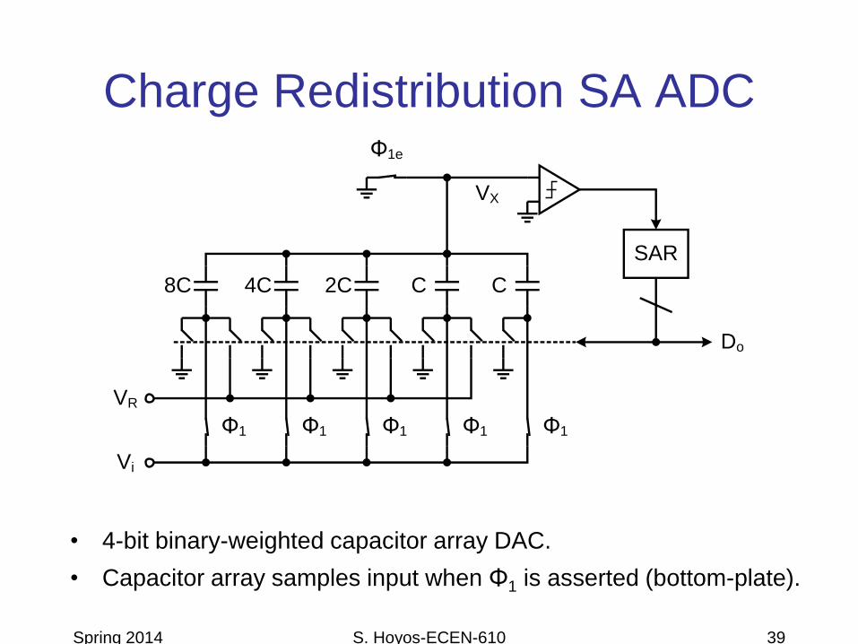
Charge Redistribution SA ADC
• 4-bit binary-weighted capacitor array DAC.
• Capacitor array samples input when Φ1 is asserted (bottom-plate).
SAR
Do
Φ1e
VX
2C C C8C 4C
VR
Vi
Φ1 Φ1 Φ1 Φ1 Φ1

Spring 2014 S. Hoyos-ECEN-610 40
Charge Redistribution (MSB)
SAR
Do
Φ1e
VX
2C C C8C 4C
VR
Vi
Φ1 Φ1 Φ1 Φ1 Φ1
iR
j
j
j
jiRX
j
jXXR
j
ji VV
CCVCVVCVCVVCV
2
4
0
4
0
4
3
0
4
4
0
Spring 2014 S. Hoyos-ECEN-610 41
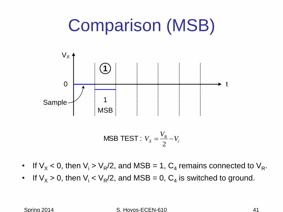
Comparison (MSB)
• If VX < 0, then Vi > VR/2, and MSB = 1, C4 remains connected to VR.
• If VX > 0, then Vi < VR/2, and MSB = 0, C4 is switched to ground.
VX
t0
1
MSBSample
1
iR
X VV
V 2
:TEST MSB
Spring 2014 S. Hoyos-ECEN-610 42
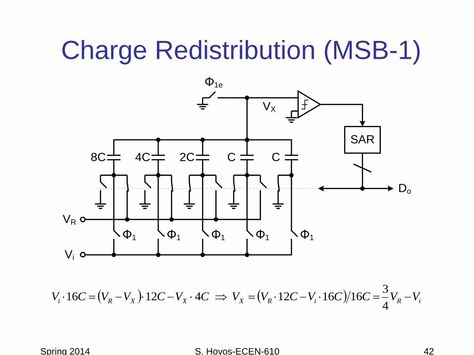
Charge Redistribution (MSB-1)
iRiRXXXRi VVCCVCVVCVCVVCV 4
316161241216
SAR
Do
Φ1e
VX
2C C C8C 4C
VR
Vi
Φ1 Φ1 Φ1 Φ1 Φ1
Spring 2014 S. Hoyos-ECEN-610 43
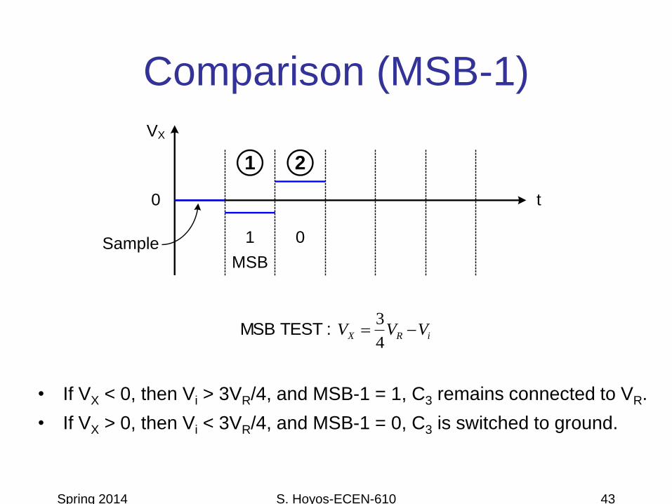
Comparison (MSB-1)
• If VX < 0, then Vi > 3VR/4, and MSB-1 = 1, C3 remains connected to VR.
• If VX > 0, then Vi < 3VR/4, and MSB-1 = 0, C3 is switched to ground.
iRX VVV 4
3 :TEST MSB
VX
t0
1 0
MSBSample
1 2

Spring 2014 S. Hoyos-ECEN-610 44
Charge Redistribution (Other Bits)
Test completes when all four bits are determined w/ four charge
redistributions and comparisons.
SAR
Do
Φ1e
VX
2C C C8C 4C
VR
Vi
Φ1 Φ1 Φ1 Φ1 Φ1
Spring 2014 S. Hoyos-ECEN-610 45
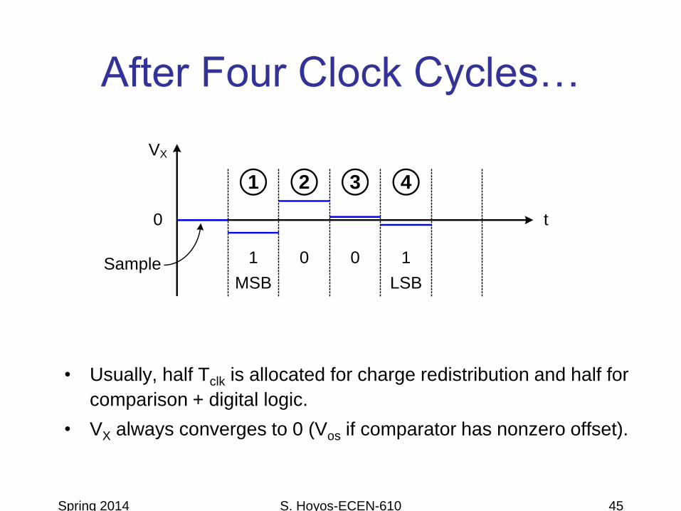
After Four Clock Cycles…
• Usually, half Tclk is allocated for charge redistribution and half for
comparison + digital logic.
• VX always converges to 0 (Vos if comparator has nonzero offset).
VX
t0
1 0 0 1
MSB LSBSample
1 2 3 4

Spring 2014 S. Hoyos-ECEN-610 46
Bottom-Plate Parasitics
• If Vos = 0, CP has no effect; otherwise, CP attenuates VX.
• AZ can be applied to the comparator to reduce offset.
SAR
Do
Φ1e
2C C C8C 4C
VR
Vi
Φ1 Φ1 Φ1 Φ1 Φ1
CP
Vos

Spring 2014 S. Hoyos-ECEN-610 47
Summary on SA ADC
• Power efficiency – only comparator consumes DC power.
• DAC nonlinearity limits the INL and DNL of the SA ADC
– N-bit precision requires N-bit matching from the cap array.
– Calibration can be performed to remove mismatch errors (Lee, JSSC 84).
• If CP=0, comparator offset Vos introduces an input-referred offset Vos;
for nonzero CP, input-referred offset is larger than Vos (δ~CP/ΣCj).
• If Vos=0, CP has no effect (VX→0 at the end of search); otherwise,
charge sharing occurs at summing node (VX is attenuated).
• Binary search is sensitive to intermediate errors made during search
– DAC must settle into ½ LSB within the time allowed.
– Comparator offset must be constant (no hysteresis).
– Nonbinary search can be used (Kuttner, ISSCC, 2002).

Spring 2014 S. Hoyos-ECEN-610 48
References
1. R. E. Suarez, P. R. Gray, and D. A. Hodges, JSSC, pp. 379-385, issue 6, 1975.
2. J. L. McCreary and P. R. Gray, JSSC, pp. 371-379, issue 6, 1975.
3. H.-S. Lee, D. A. Hodges, and P. R. Gray, JSSC, pp. 813-819, issue 6, 1984.
4. M. de Wit, K.-S. Tan, and R. K. Hester, JSSC, pp. 455-461, issue 4, 1993.
5. C. M. Hammerschmied and H. Qiuting, JSSC, pp. 1148-1157, issue 8, 1998.
6. S. Mortezapour and E. K. F. Lee, JSSC, pp. 642-646, issue 4, 2000.
7. G. Promitzer, JSSC, pp. 1138-1143, issue 7, 2001.
8. F. Kuttner, ISSCC, 2002, pp. 176-177.

Spring 2014 S. Hoyos-ECEN-610 49
Algorithmic ADC
Spring 2014 S. Hoyos-ECEN-610 50
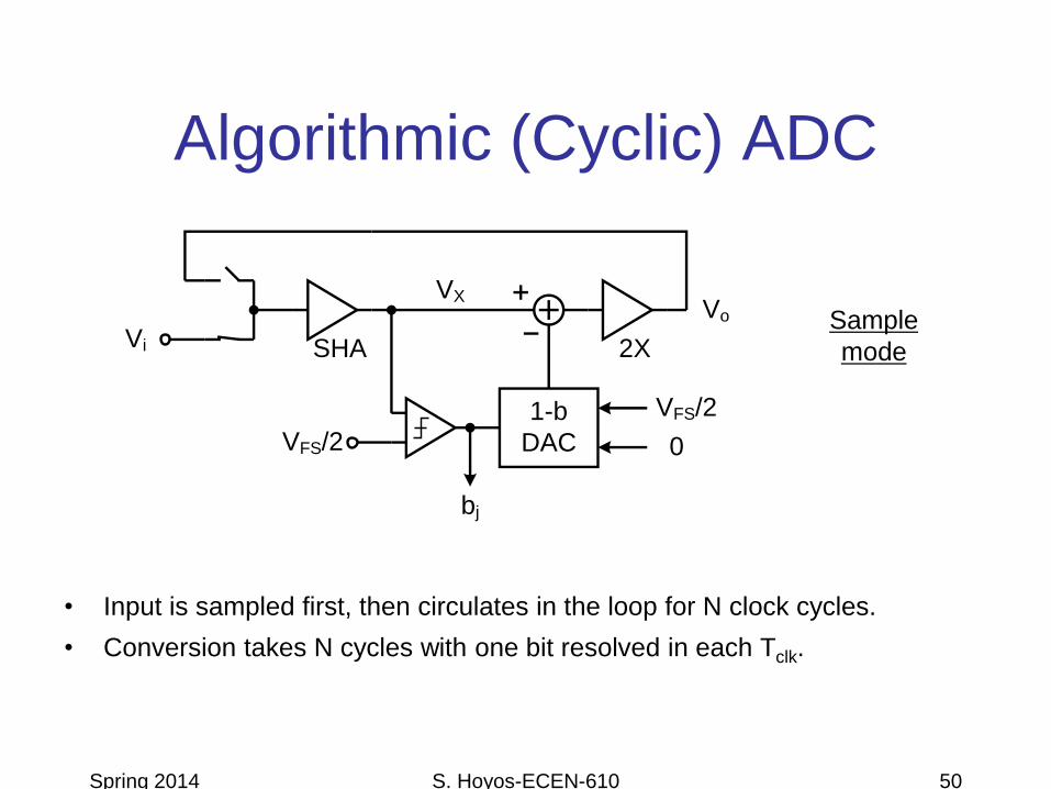
Algorithmic (Cyclic) ADC
• Input is sampled first, then circulates in the loop for N clock cycles.
• Conversion takes N cycles with one bit resolved in each Tclk.
Vi
VFS/2
Vo
bj
1-b
DACVFS/2 0
SHA 2X
VX
Sample
mode
Spring 2014 S. Hoyos-ECEN-610 51
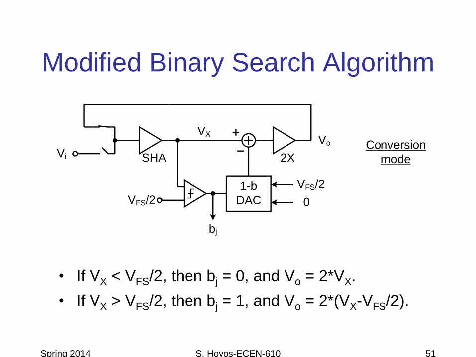
Modified Binary Search Algorithm
• If VX < VFS/2, then bj = 0, and Vo = 2*VX.
• If VX > VFS/2, then bj = 1, and Vo = 2*(VX-VFS/2).
Conversion
modeVi
VFS/2
Vo
bj
1-b
DACVFS/2 0
SHA 2X
VX

Spring 2014 S. Hoyos-ECEN-610 52
Modified Binary Search Algorithm
• Constant threshold (VFS/2) is used for each comparison.
• 2X gain is provisioned each time residue circulates around the loop.
VX
Vi
0
VFS
1 0 0 1 1 0MSB LSBTclk
VFS
2
X2 X2 X2 X2 X21 42 63 5

Spring 2014 S. Hoyos-ECEN-610 53
Loop Transfer Function
• If VX < VFS/2, then bj = 0, and Vo = 2*VX.
• If VX > VFS/2, then bj = 1, and Vo = 2*(VX-VFS/2).
Vi
VFS/2
Vo
bj
1-b
DACVFS/2 0
SHA 2X
VX
c
Vi
Vo
VFS/20 VFS
VFS
bj=0 bj=1

Spring 2014 S. Hoyos-ECEN-610 54
Offset ErrorsIdeal RA offset CMP offset
Vo = 2*(Vi - bj*VFS/2) → Vi = bj*VFS/2 + Vo/2
Vi
Vo
VFS/20 VFS
VFS
b=0 b=1
Vi
Vo
VFS/20 VFS
VFS
b=0 b=1
Vi
Vo
VFS/20 VFS
VFS
b=0 b=1Vos
Vos
Vi
Do
VFS/20 VFS Vi
Do
VFS/20 VFS Vi
Do
VFS/20 VFS

Spring 2014 S. Hoyos-ECEN-610 55
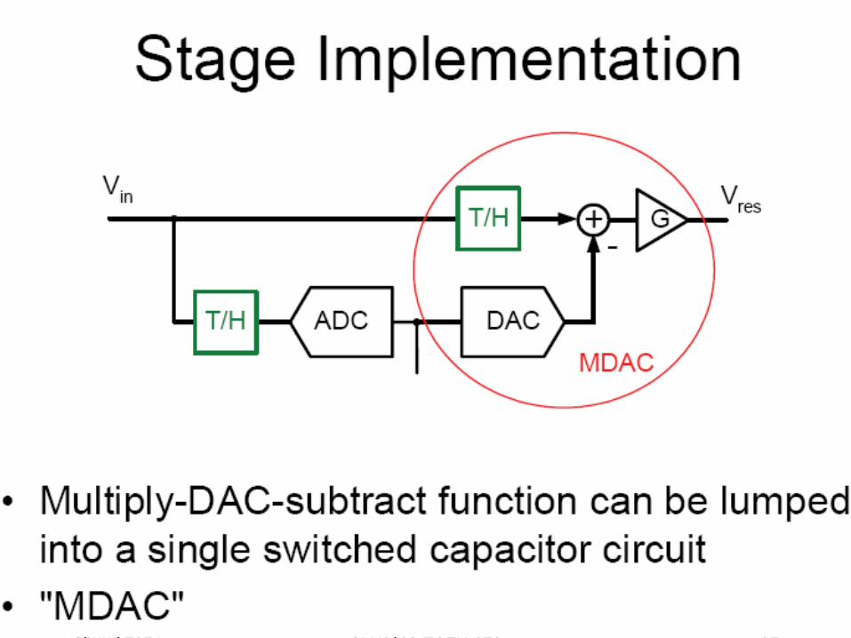
The Multiplier DAC (MDAC)
• 2X gain + 3-level DAC + subtraction all integrated.
• A 3-level DAC is perfectly linear w/ fully-differential signals.
Vo
Vi
0-VR
VR
Decoder
Φ1 C1
Φ1 C2
Φ2
Φ1e
A
Φ2
-VR/4
VR/4
Spring 2014 S. Hoyos-ECEN-610 56
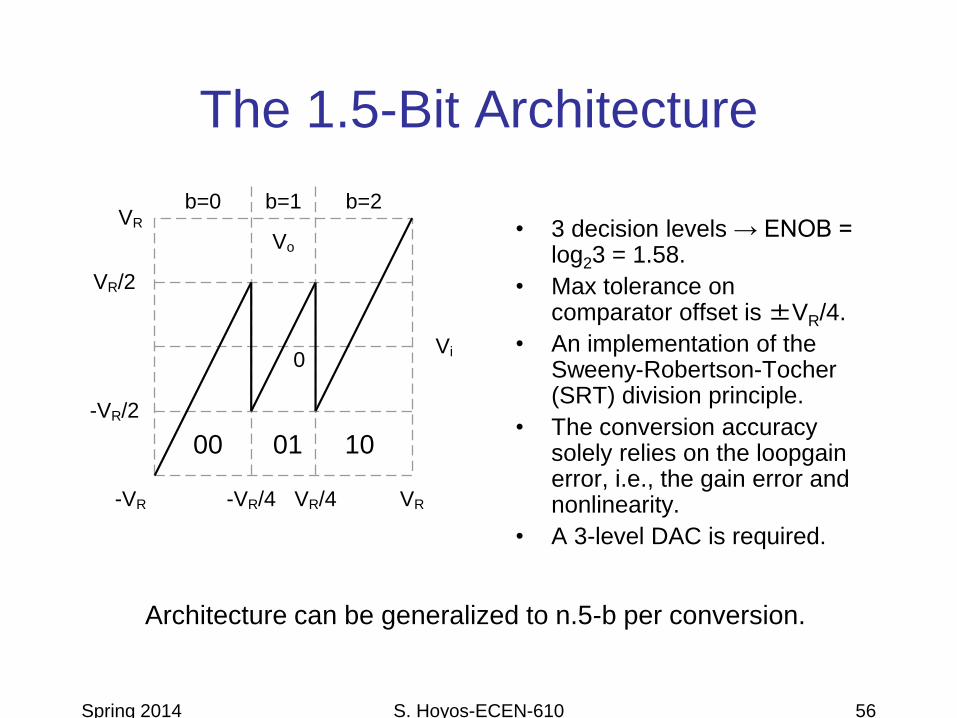
The 1.5-Bit Architecture
• 3 decision levels → ENOB = log23 = 1.58.
• Max tolerance on comparator offset is ±VR/4.
• An implementation of the Sweeny-Robertson-Tocher (SRT) division principle.
• The conversion accuracy solely relies on the loopgain error, i.e., the gain error and nonlinearity.
• A 3-level DAC is required.
Architecture can be generalized to n.5-b per conversion.
-VR/4 VR/4
0
VR/2
-VR/2
Vi
-VR
VR
VR
b=0 b=2b=1
Vo
00 1001

Spring 2014 S. Hoyos-ECEN-610 57
Error Mechanisms of RA
• Capacitor mismatch
• Op-amp finite-gain error and nonlinearity
• Charge injection and clock feedthrough
• Finite circuit bandwidth
R
1
2i
1
21o V
C
C1bV
C
CCV
i
o
211
R2i21o VΔV
VA
CCC
VC1bVCCtV
Vo
Vi
0-VR
VR
Decoder
Φ1 C1
Φ1 C2
Φ2
Φ1e
A
Φ2
-VR/4
VR/4

Spring 2014 S. Hoyos-ECEN-610 58
RA Gain Error and Nonlinearity
Raw accuracy is usually limited to 10-12 bits w/o error correction.
-VR/4 VR/4
0
VR/2
-VR/2
Vi
-VR
VR
VR
b=0 b=2b=1
Vo
0
Vi-VR VR
Do
Spring 2014 S. Hoyos-ECEN-610 59
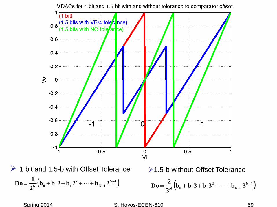
1N
1N
2
110N2b2b2bb
2
1Do
1N
1N
2
110N3b3b3bb
3
2Do
1 bit and 1.5-b with Offset Tolerance 1.5-b without Offset Tolerance
Spring 2014 S. Hoyos-ECEN-610 60
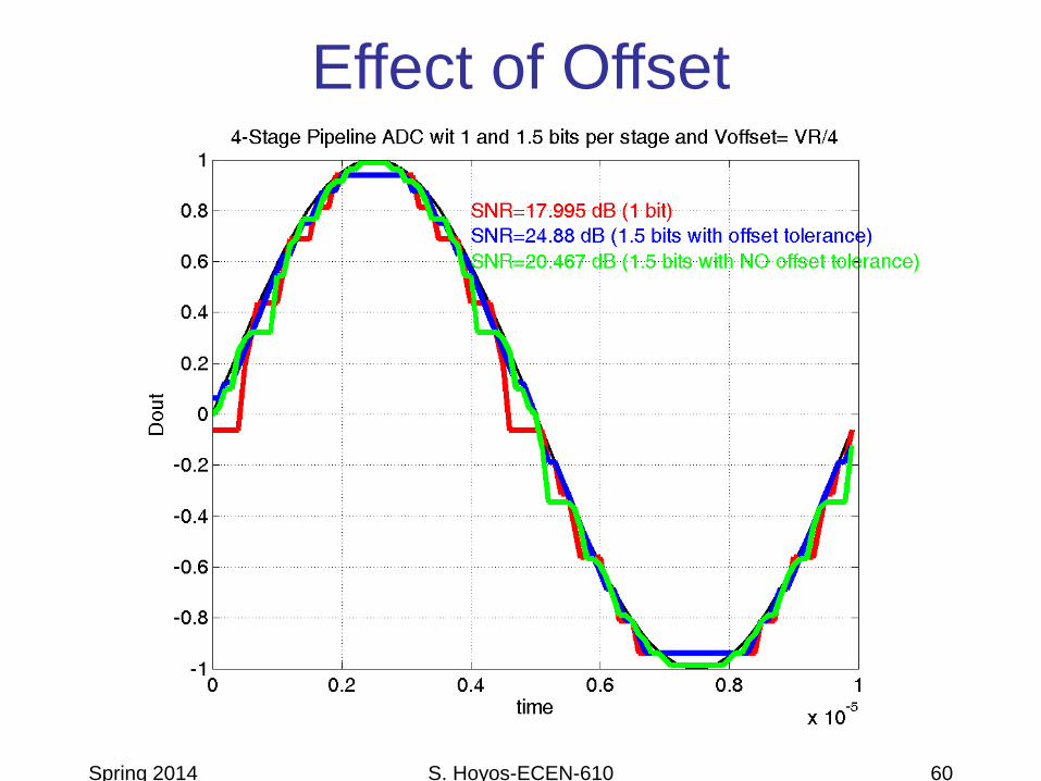
Effect of Offset

Spring 2014 S. Hoyos-ECEN-610 61
Effect of Offset

Spring 2014 S. Hoyos-ECEN-610 62
References
1. P. W. Li, et al., JSSC, vol. 19, pp. 828-836, issue 6, 1984.
2. C. Shih, et al., JSSC, vol. 21, pp. 544-554, issue 4, 1986.
3. H. Ohara, et al., JSSC, vol. 22, pp. 930-938, issue 6, 1987.
4. H. Onodera, et al., JSSC, vol. 23, pp. 152-158, issue 1, 1988.
5. B.-S. Song, et al., JSSC, vol. 23, pp. 1324-1333, issue 6, 1988.
6. B. Ginetti, et al., JSSC, vol. 27, pp. 957-964, issue 7, 1992.
7. S. H. Lewis, et al., JSSC, vol. 27, pp. 351-358, issue 3, 1992.
8. A. N. Karanicolas, et al., JSSC, vol. 28, pp. 1207-1215, issue 12, 1993.
9. H.-S. Lee, JSSC, vol. 29, pp. 509-515, issue 4, 1994.
10.S.-Y. Chin et al., JSSC, vol. 31, pp. 1201-1207, issue 8, 1996.
11.O. E. Erdogan, et al., JSSC, vol. 34, pp. 1812-1820, issue 12, 1999.

Spring 2014 S. Hoyos-ECEN-610 63
Algorithmic ADC
• Hardware-efficient, but relatively low conversion speed.
• Binary search algorithm.
• Loopgain (2X) requires the use of a residue amplifier, but greatly simplifies the DAC – 1-bit, inherently linear.
• Residue gets amplified each time it circulates the loop; the gain makes the later conversion steps (the LSB’s) insensitive to circuit noise and distortion.
• Conversion errors (residue error due to loopgain nonidealities and comparator offset) made in the earlier conversion cycles also get amplified again and again – overall accuracy is usually limited by the MSB resolving and residue generation step.
• Digital redundancy is often used to treat comparator/loop offsets.
• Trimming/calibration/ratio-independent techniques are often used to treat loopgain error.
Spring 2014 S. Hoyos-ECEN-610 64
Precision Techniques
Spring 2014 S. Hoyos-ECEN-610 65
Ratio-Independent Multiply-By-N Circuit
• Steps (1) and (2) are repeated for N times.
• C2 functions as a temporary charge storage.
Sampling Charge transfer C1-C2 exchanged
Vi Vo(1) Vo(2)
C2
A
C1
C2
A
C1
Vo(3)
C1
A
C2
(1) (2) (3)

Spring 2014 S. Hoyos-ECEN-610 66
RA Gain Trimming
• Precise gain-of-two is achieved by adjustment of the trim array.
• Finite-gain error of op-amp is also compensated (not nonlinearity).
C1/C2 = 2
nominallyVo
-
Vo+
Vi+
Vi-
Trim
array
VX+
VX-
A
C2C1
C2C1

Spring 2014 S. Hoyos-ECEN-610 67
Split-Array Trimming DAC
• Successive approximation is performed to find the correct gain setting.
• Coupling cap is slightly increased to ensure segment overlap.
2C1.2C
8C4C2CC8C4C2CC
2C1.2C
8C4C2CC8C4C2CC
VX+
VX-
Vi+
Vi-
8-bit gain
setting + sign
Spring 2014 S. Hoyos-ECEN-610 68
Digital Calibration
• RA gain is set lower than 2X, forcing missing codes but NOT
missing decision levels.
• Calibration is performed by measuring distance between S1 and S2;
(S2-S1) is later subtracted from Do (gain error and offset remain).
0Vi
-VR
VR
VR
MSB=0 MSB=1Vo
0
Vi-VR VR
Do
S1
S1
S2
S2
MSB=0
MSB=1

Spring 2014 S. Hoyos-ECEN-610 69
Digital Calibration
• C1 = C2
• C3 = βC1
• AZ SC amplifier
β1
V12b2V
CC
VC12bVCCV
Ri
32
R1i21o
Residue Amplifier
Vo
Vi
-VR
VR
Φ1 C2
Φ1 C1
Φ2
A
C3
Φ1e
Decoder
Φ1e
Φ2
Φ2
Spring 2014 S. Hoyos-ECEN-610 70
Capacitor Error-Averaging
,VVδV2V
C
VCVCCV RiRi
1
R2i21x1
Vx1VR Vx2
VR
A1
C1
C2
A1
C2
C1
Vi
A1
C1
C2
Φ1 Φ2 Φ3
Vx1
Φ1 Φ2
+Δ-Δ
Φ3
2Vi-VR
Vx2 .VVδV2V
C
VCVCCV RiRi
2
R1i21x2
,Cδ1C 12
Inherently linear capacitor error-averaging techniques for pipelined A/D conversion Yun Chiu;Circuits and Systems II:
Analog and Digital Signal Processing, IEEE Transactions on Volume 47, Issue 3, March 2000 Page(s):229 - 232

Spring 2014 S. Hoyos-ECEN-610 71
Capacitor Error-Averaging
,V2V2
VVV Ri
x2x1o
Φ2 Φ3
,CVCVCCV 4x23o43x1
,C2C 43
Vo
A2
C3
C4
-1
A2
C3
C4
-1Vx1 Vx2
Φ1 Φ2
Vo
Φ3
2Vi-VR

Spring 2014 S. Hoyos-ECEN-610 72
Capacitor Error-Averaging
33 δ1C2C 44 δ1CC 11 δ1C C 22 δ1C C
Assume , , , , are zero mean Gaussian with
variance .
Find an expression for Vo and comment on the
effectiveness of the capacitor error-averaging technique.
1δ 2δ 3δ 4δ
2

Spring 2014 S. Hoyos-ECEN-610 73
References
1. P. W. Li, et al., JSSC, vol. 19, pp. 828-836, issue 6, 1984.
2. C. Shih, et al., JSSC, vol. 21, pp. 544-554, issue 4, 1986.
3. H. Ohara, et al., JSSC, vol. 22, pp. 930-938, issue 6, 1987.
4. H. Onodera, et al., JSSC, vol. 23, pp. 152-158, issue 1, 1988.
5. B.-S. Song, et al., JSSC, vol. 23, pp. 1324-1333, issue 6, 1988.
6. B. Ginetti, et al., JSSC, vol. 27, pp. 957-964, issue 7, 1992.
7. S. H. Lewis, et al., JSSC, vol. 27, pp. 351-358, issue 3, 1992.
8. A. N. Karanicolas, et al., JSSC, vol. 28, pp. 1207-1215, issue 12, 1993.
9. H.-S. Lee, JSSC, vol. 29, pp. 509-515, issue 4, 1994.
10.S.-Y. Chin et al., JSSC, vol. 31, pp. 1201-1207, issue 8, 1996.
11.O. E. Erdogan, et al., JSSC, vol. 34, pp. 1812-1820, issue 12, 1999.
Spring 2014 S. Hoyos-ECEN-610 74
Subranging ADC

Spring 2014 S. Hoyos-ECEN-610 75
Subranging ADC Architecture
Vi
VRT
VRB
Co
ars
e E
nco
de
r
Fine Encoder
MSB’s
LSB’s
Fine
Flash
Coarse
Flash

Spring 2014 S. Hoyos-ECEN-610 76
Subranging ADCPros
• Reduced complexity – 2*(2N/2-1) comparators
• Reduced Cin, area, and power consumption
• No residue amplifier required
Cons
• Typically 3 clock phases per conversion
– Sample
– Coarse comparison
– Fine comparison
• THA required (two-stage S/H if the front-end SHA only holds for one phase)
• Offset tolerance on fine comparators is at N-bit level.
• Offset tolerance on coarse comparators is also at N-bit level without digital redundancy.

Spring 2014 S. Hoyos-ECEN-610 77
Example Block Diagram
Do
Re
fere
nce
La
dd
er Coarse
ADC
En
co
de
r
Fine ADC
ViVRT
MSB’s
LSB’s
SHA
VRB
SHA
MUX
4 bits
5 bits
8 bits
Redundancy in fine ADC provided by over- and under-range comparators

Spring 2014 S. Hoyos-ECEN-610 78
Digital Redundancy of Fine ADC
Search range of the fine ADC is extended on both sides.
…
Vi
Fine Encoder + Error Correction
Extra
CMP’s
Extra
CMP’s
…
…
To
Coarse
CMP’s
… …
VR1
VR2
Spring 2014 S. Hoyos-ECEN-610 79
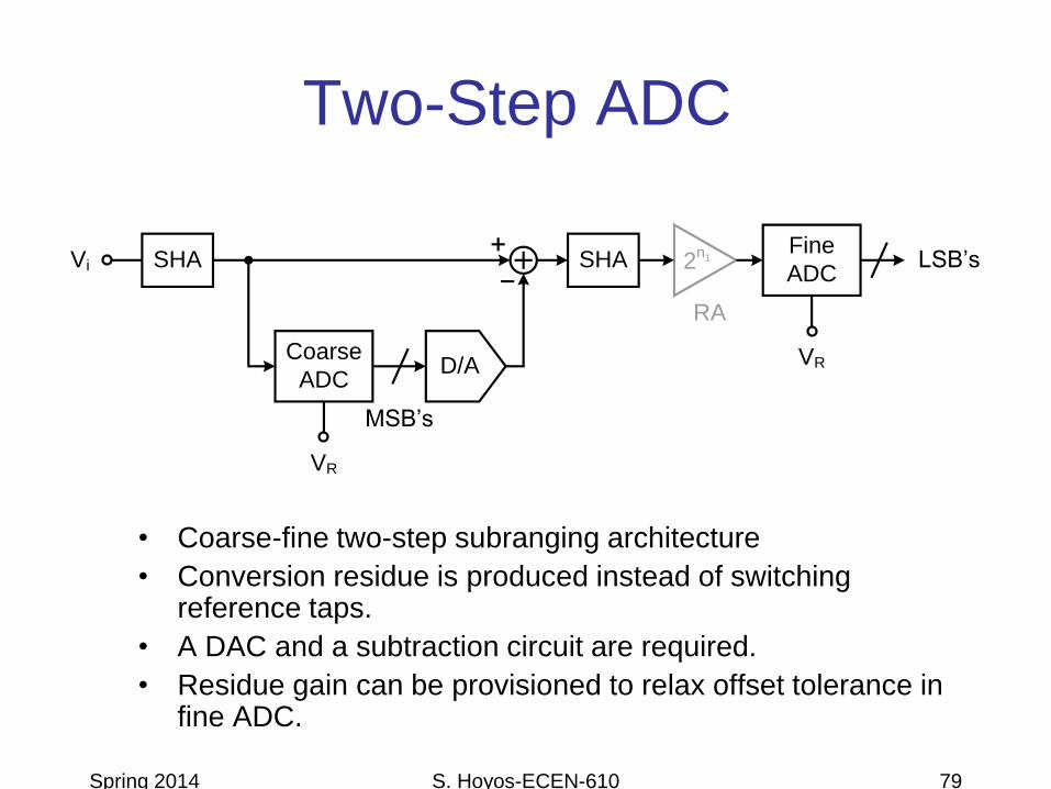
Two-Step ADC
Coarse
ADC
Fine
ADCVi
MSB’s
LSB’sSHA
VR
RA
2n1
D/A
SHA
VR
• Coarse-fine two-step subranging architecture
• Conversion residue is produced instead of switching reference taps.
• A DAC and a subtraction circuit are required.
• Residue gain can be provisioned to relax offset tolerance in fine ADC.

Spring 2014 S. Hoyos-ECEN-610 80
Timing Diagram
Sample
Vi
Coarse
ADC
DAC + RA
Fine ADC
• Four conversion steps can be pipelined.
• Usually DAC + RA settling takes the longest time.
• RA is often omitted (residue gain of one) to speed up conversion.

Spring 2014 S. Hoyos-ECEN-610 81
References1. A. G. F. Dingwall et al., JSSC, vol. 20, pp. 1138-1143, issue 6, 1985.
2. J. Doernberg et al., JSSC, vol. 24, pp. 241-249, issue 2, 1989.
3. B.-S. Song et al., JSSC, vol. 25, pp. 1328-1338, issue 6, 1990.
4. T. Matsuura et al., CICC, 1990, pp. 6.4/1-6.4/4.
5. B. Razavi et al., JSSC, vol. 27, pp. 1667-1678, issue 12, 1992.
6. C. Mangelsdorf et al., ISSCC, 1993, pp. 64-65.
7. W. T. Colleran et al., JSSC, vol. 28, pp. 1187-1199, issue 12, 1993.
8. K. Kusumoto et al., JSSC, vol. 28, pp. 1200-1206, issue 12, 1993.
9. K. Sone et al., ISSCC, 1993, pp. 66 - 67, 264.
10.R. Jewett et al., ISSCC, 1997, pp. 138-139, 443.
11.B. P. Brandt et al., JSSC, vol. 34, pp. 1788-1795, issue 12, 1999.
12.H. Pan et al., JSSC, vol. 35, pp. 1769-1780, issue 12, 2000.
13.R. C. Taft et al., JSSC, vol. 36, pp. 331, issue 3, 2001.
14.H. van der Ploeg et al., JSSC, vol. 36, pp. 1859-1867, issue 12, 2001.
15.J. Mulder et al., JSSC, vol. 39, pp. 2116-2125, issue 12, 2004.

Spring 2014 S. Hoyos-ECEN-610 82
Pipeline ADC

Spring 2014 S. Hoyos-ECEN-610 83
Pipeline ADC Architecture
• A multi-stage subranging ADC with inter-stage gain
• An unrolled algorithmic ADC
n1 bits n2 bits nk bits
V1
V2 Vk-1...
Vin V3
n2 bits
V1
V2
Residue
amp
Stage
1
Stage
2
Stage
k
2n2S/H
A/D D/A
n3 bits
Stage
3

Spring 2014 S. Hoyos-ECEN-610 84
Pipeline Timing Diagram
S1 samples
S1 DAC+RA
S2 samples
S1 samples
S2 DAC+RA
S3 samples
S1 DAC+RA
S2 samples
S3 DAC+RA
S1 CMP S2 CMPS1 CMP
S3 CMP
Φ1
Φ2
• Two-phase nonoverlapping clock is typically used, with the coarse ADC’s operating within the nonoverlapping times.
• All pipeline stages operate simultaneously, increasing throughput (at the cost of latency).
Spring 2014 S. Hoyos-ECEN-610 85
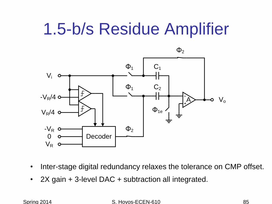
1.5-b/s Residue Amplifier
• Inter-stage digital redundancy relaxes the tolerance on CMP offset.
• 2X gain + 3-level DAC + subtraction all integrated.
Vo
Vi
0-VR
VR
Decoder
Φ1 C1
Φ1 C2
Φ2
Φ1e
A
Φ2
-VR/4
VR/4

Spring 2014 S. Hoyos-ECEN-610 86

Spring 2014 S. Hoyos-ECEN-610 87

Spring 2014 S. Hoyos-ECEN-610 88

Spring 2014 S. Hoyos-ECEN-610 89

Spring 2014 S. Hoyos-ECEN-610 90
Spring 2014 S. Hoyos-ECEN-610 91
Spring 2014 S. Hoyos-ECEN-610 92

Spring 2014 S. Hoyos-ECEN-610 93
2.5-b/s Residue Amplifier
Vo
Vi
0
-VR
VR
Decoder
Φ1e
A
Φ2
VR6
VR1
6 CMP’s
...
Φ1 C1
Φ1 C2
Φ2
C3
C4
Φ1
Φ1
Φ2
Φ2
Spring 2014 S. Hoyos-ECEN-610 94
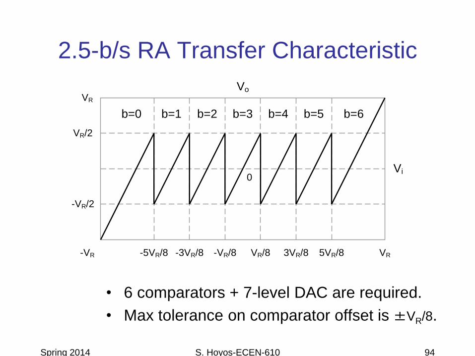
2.5-b/s RA Transfer Characteristic
• 6 comparators + 7-level DAC are required.
• Max tolerance on comparator offset is ±VR/8.
b=1 b=3 b=5b=0 b=2 b=4 b=6
Vi
Vo
-5VR/8 VR/8
VR/2
-VR/2
0
-3VR/8 -VR/8 5VR/83VR/8-VR VR
VR
Spring 2014 S. Hoyos-ECEN-610 95
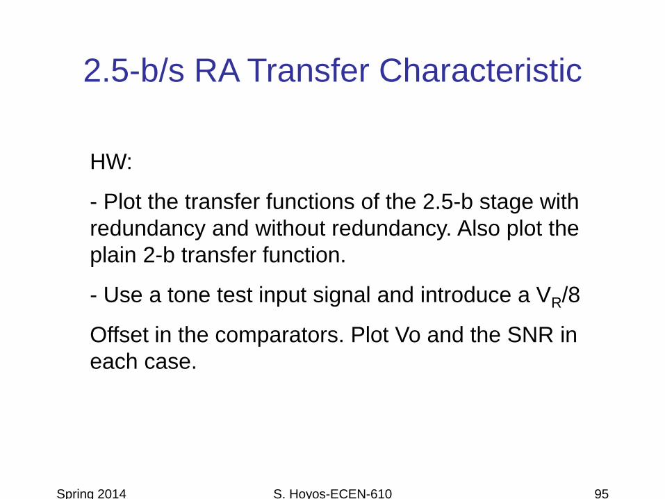
2.5-b/s RA Transfer Characteristic
HW:
- Plot the transfer functions of the 2.5-b stage with
redundancy and without redundancy. Also plot the
plain 2-b transfer function.
- Use a tone test input signal and introduce a VR/8
Offset in the comparators. Plot Vo and the SNR in
each case.

Spring 2014 S. Hoyos-ECEN-610 96
RA Gain Error and Nonlinearity
• Raw accuracy is usually limited to 10-12 bits w/o error correction.
• Similar correction techniques applied to algorithmic ADC can be used.
-VR/4 VR/4
0
VR/2
-VR/2
Vi
-VR
VR
VR
b=0 b=2b=1
Vo
0
Vi-VR VR
Do

Spring 2014 S. Hoyos-ECEN-610 97
Front-End Clock Skew
bits/stage 1.5 2.5 3.5
err.-corr.
range
±VFS
4
±VFS
8
±VFS
16
# of cmps 2 6 14
• Digital redundancy allows tolerance on sampling clock skew.
• Dedicated front-end SHA can be used to eliminate the problem, but
introduces power and area overhead.
Spring 2014 S. Hoyos-ECEN-610 98
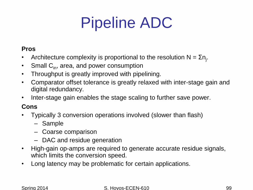
Spring 2014 S. Hoyos-ECEN-610 99
Pipeline ADC
Pros
• Architecture complexity is proportional to the resolution N = Σnj.
• Small Cin, area, and power consumption
• Throughput is greatly improved with pipelining.
• Comparator offset tolerance is greatly relaxed with inter-stage gain and digital redundancy.
• Inter-stage gain enables the stage scaling to further save power.
Cons
• Typically 3 conversion operations involved (slower than flash)
– Sample
– Coarse comparison
– DAC and residue generation
• High-gain op-amps are required to generate accurate residue signals, which limits the conversion speed.
• Long latency may be problematic for certain applications.
Spring 2014 S. Hoyos-ECEN-610 100
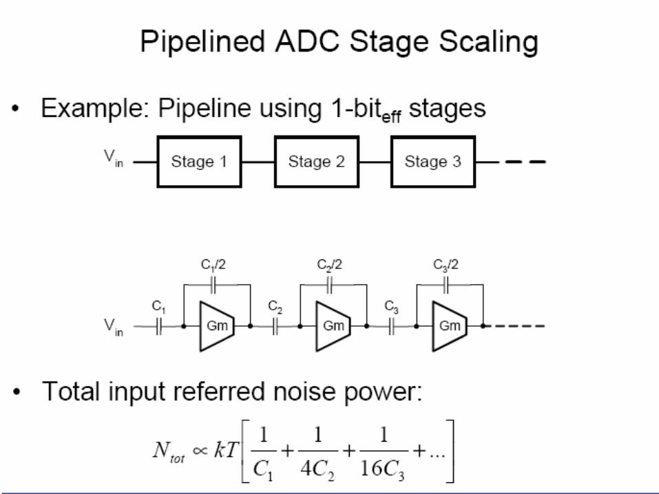
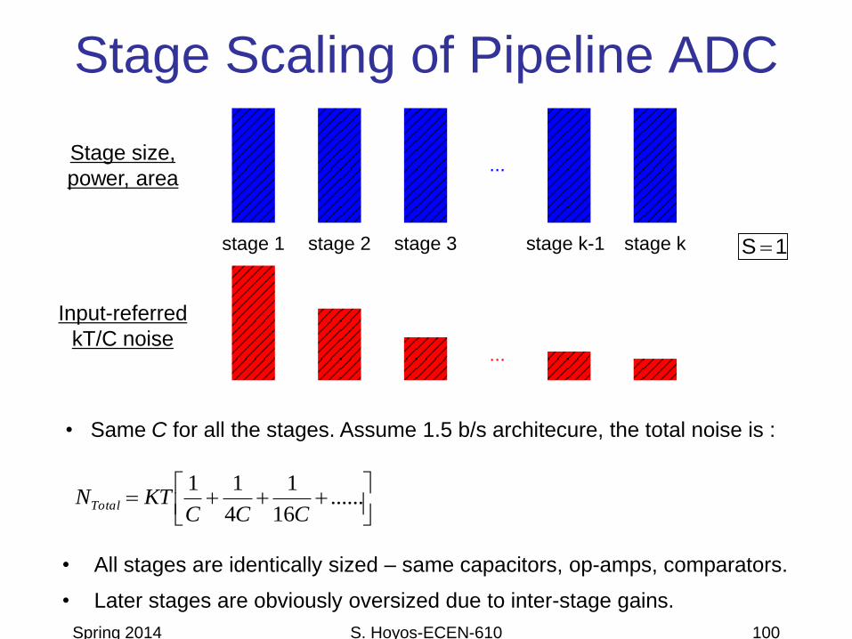
Stage Scaling of Pipeline ADC
• All stages are identically sized – same capacitors, op-amps, comparators.
• Later stages are obviously oversized due to inter-stage gains.
stage 3stage 1 stage 2 stage kstage k-1
...
...
Stage size,
power, area
Input-referred
kT/C noise
1S
......
16
1
4
11
CCCKTNTotal
• Same C for all the stages. Assume 1.5 b/s architecure, the total noise is :
Spring 2014 S. Hoyos-ECEN-610 101
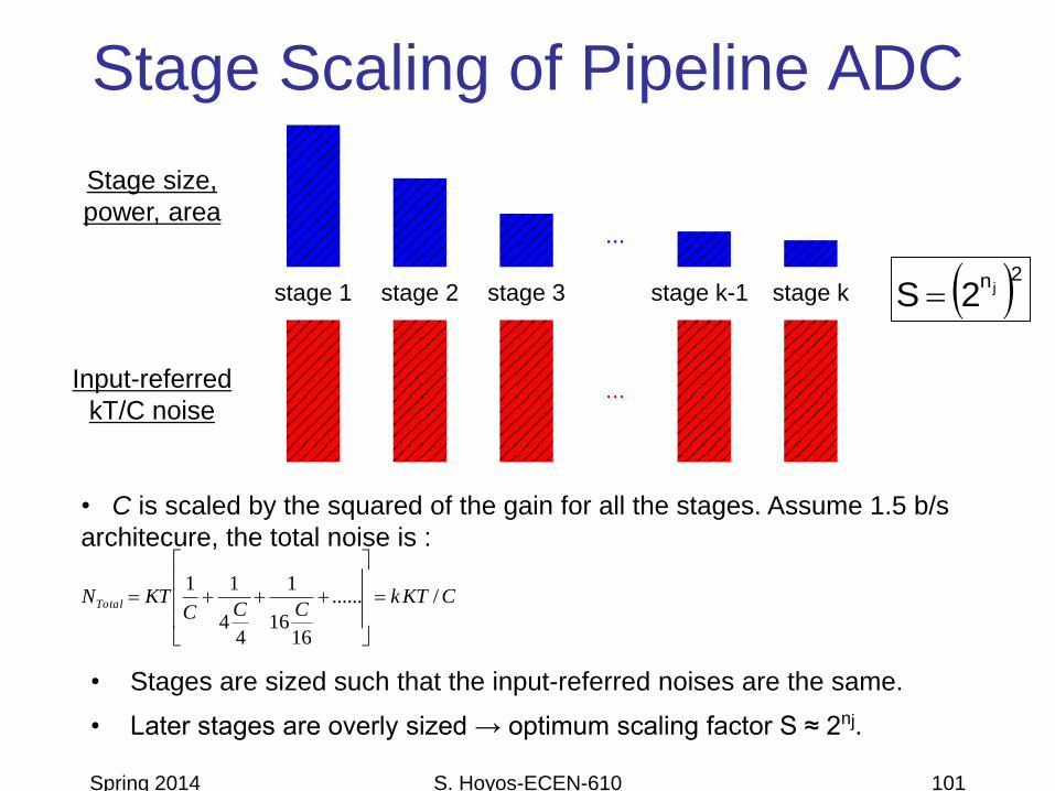
Stage Scaling of Pipeline ADC
• Stages are sized such that the input-referred noises are the same.
• Later stages are overly sized → optimum scaling factor S ≈ 2nj.
Stage size,
power, area
Input-referred
kT/C noise
stage 3stage 1 stage 2 stage kstage k-1
...
...
2n j2S
CKTkCCC
KTNTotal /......
1616
1
44
11
• C is scaled by the squared of the gain for all the stages. Assume 1.5 b/s
architecure, the total noise is :

Spring 2014 S. Hoyos-ECEN-610 102
Stage Scaling of Pipeline ADC
CKTnCCC
KTN fTotal /6......
1616
1
44
11
• Optimum scaling will be somewhere from scaling by the gain squared and
scaling by just the gain.
• Need to take into account other sources of noise in the overall expression.
• Example: for 6 stages of 2.5b/s, if we assume scaling by interstage gain of 16
to get equal noise contribution from each stage. Total noise will be:
......
416
1
24
11
CCCKTNTotal
• If C is scaled by the gain for all the stages and assuming 1.5 b/s
architecure, the total noise is :
pFC
VV
C
KT
VSNR
in
pp
in
pp
5.2
2
12
6
8/2
2
Spring 2014 S. Hoyos-ECEN-610 103
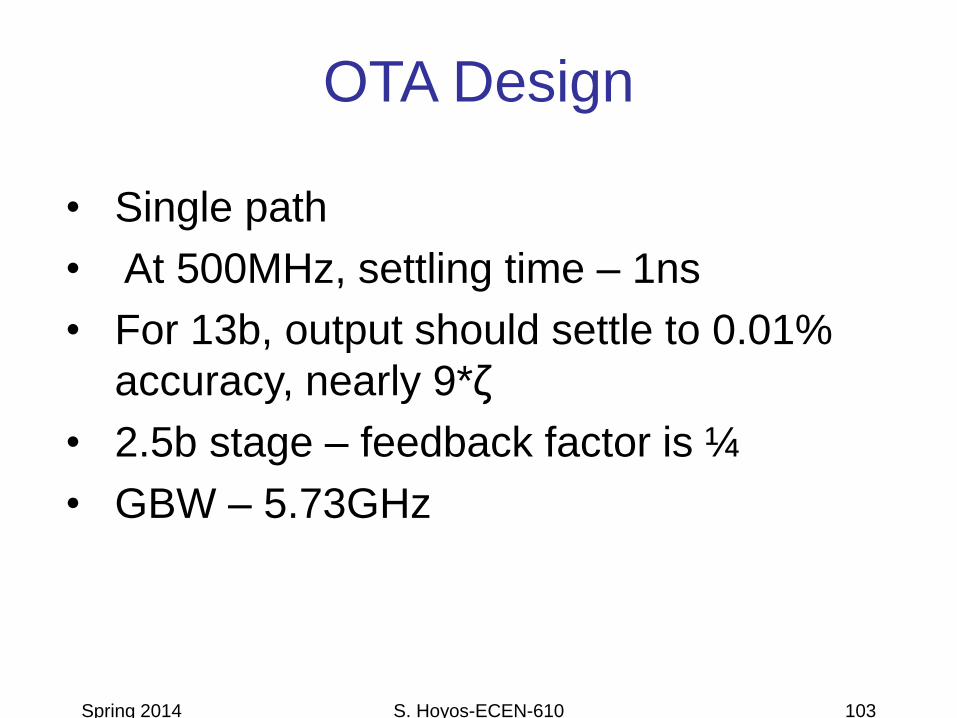
OTA Design
• Single path
• At 500MHz, settling time – 1ns
• For 13b, output should settle to 0.01%
accuracy, nearly 9*ζ
• 2.5b stage – feedback factor is ¼
• GBW – 5.73GHz

Spring 2014 S. Hoyos-ECEN-610 104
OTA Design
• Dual path – Time interleaving
• At 250MHz, settling time – 2ns
• For 13b, output should settle to 0.01%
accuracy, nearly 9*ζ
• 1.5b stage – feedback factor is 1/2
• GBW – 1.43GHz
Spring 2014 S. Hoyos-ECEN-610 105
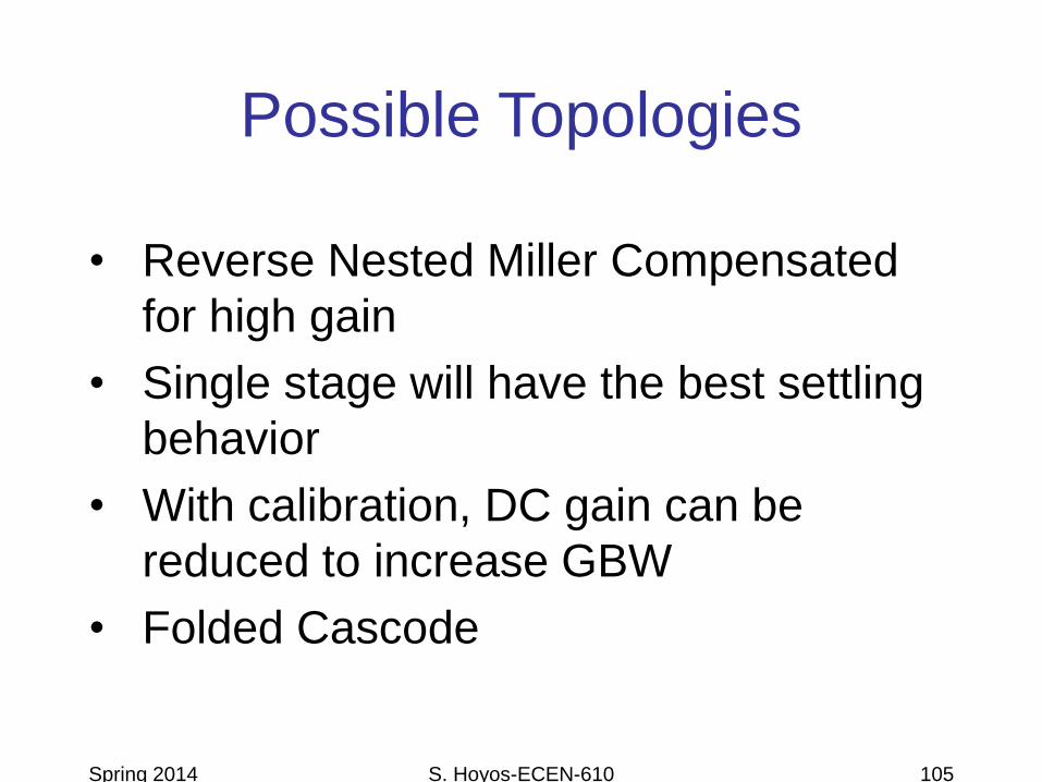
Possible Topologies
• Reverse Nested Miller Compensated
for high gain
• Single stage will have the best settling
behavior
• With calibration, DC gain can be
reduced to increase GBW
• Folded Cascode

Spring 2014 S. Hoyos-ECEN-610 106
References
• D. W. Cline and P. R. Gray, "A power optimized 13-b 5-Msamples/spipelined analog-to-digital converter in 1.2-μm CMOS," IEEE Journalof Solid-State Circuits, vol. 31, no. 3, pp. 294-303, Mar. 1996.
• kT/C Constrained Optimization of Power in Pipeline ADCs - Yu Lin,Vipul Katyal, Randall Geiger Dept. Electrical and Computer Engineering,Iowa State University Ames, IA, 50010, USA Mark Schlarmann FreescaleSemiconductor, Inc.
• Kwok, P.T. F. and Luong, Howard C, “Power Optimization for PipelineAnalog-to-Digital Converters”, IEEE transactions on circuits andsystems II: Analog and digital signal processing, Vol. 46, No. 5, May 1999,pp. 549-553
• Background Digital Error Correction Technique For PipelinedAnalog-digital Converters Sameer R. Sonkusale and Jan Van derSpiegel
• Digital Background Calibration Technique for Pipeline ADCs withMulti-bit Stages Antonio J. Ginés, Eduardo J. Peralías and AdoraciónRueda

Spring 2014 S. Hoyos-ECEN-610 107
Pipeline Calibration Methods
• Foreground
Calibration
• Interruption of ADC signal
• Cannot correct for
environmental changes
and variations with time
• E.g. – Radix based
• Background Calibration
• Works without interruption of normal operation
• E.g. - LMS based
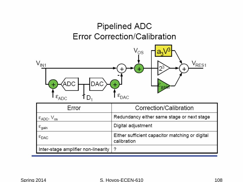
Spring 2014 S. Hoyos-ECEN-610 108

Spring 2014 S. Hoyos-ECEN-610 109

Spring 2014 S. Hoyos-ECEN-610 110

Spring 2014 S. Hoyos-ECEN-610 111
LMS based calibration
ADC
Analog
Input
Adaptive
Dig. Filter
“Channel” Adaptive Equalizer
x(n)
y(n)
d(n)
e(n)
↓nRef.
ADC
↓n

Spring 2014 S. Hoyos-ECEN-610 112
Single Stage Calibration
Calibration of a single stage at a time
Different variations of LMS to reduce computational complexity
Spring 2014 S. Hoyos-ECEN-610 113
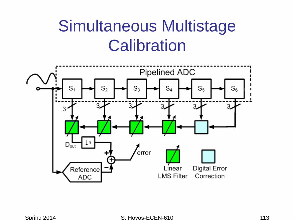
Simultaneous Multistage
Calibration

Spring 2014 S. Hoyos-ECEN-610 114
Matlab Simulations
0 500 1000 1500 2000 2500 3000 3500 4000 4500 5000-350
-300
-250
-200
-150
-100
-50
0
50
100
frequency
Am
plit
ude
DFT plot before calibration
0 200 400 600 800 1000 1200 1400-120
-100
-80
-60
-40
-20
0
20
40
60
80
FrequencyA
mplit
ude
DFT plot after calibration
Without offset and finite gain
SNR – 45.74dB SNR – 77.26dB
Spring 2014 S. Hoyos-ECEN-610 115
Matlab Simulations
0 1000 2000 3000 4000 5000 6000 7000 8000 9000 10000-0.01
-0.008
-0.006
-0.004
-0.002
0
0.002
0.004
0.006
0.008
0.01Error between filter output and expected output
Iteration
Err
or
0 1000 2000 3000 4000 5000 6000 7000 8000 9000 100000.235
0.24
0.245
0.25
0.255
0.26
0.265Weights
IterationW
eig
ht
valu
e
Final Weights - 0.2479 0.2612 0.2368 0.2635 0.2483 0.2488
Non-ideal Weights - 0.2564 0.2424 0.2597 0.2469 0.2532 0.2632
Spring 2014 S. Hoyos-ECEN-610 116
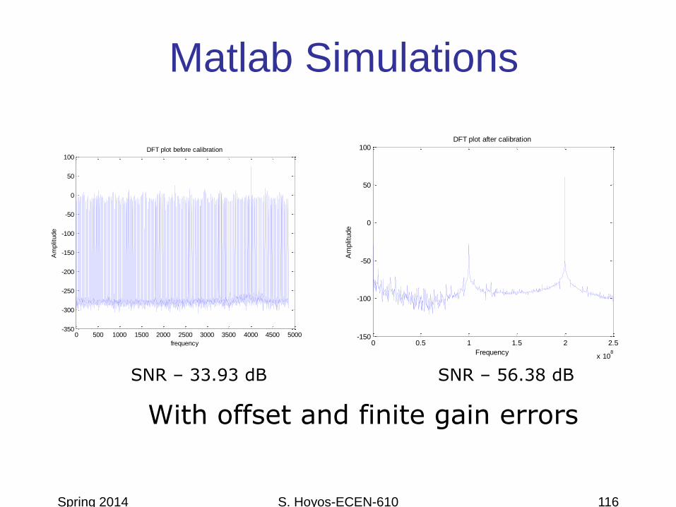
Matlab Simulations
SNR – 33.93 dB SNR – 56.38 dB
With offset and finite gain errors
0 0.5 1 1.5 2 2.5
x 108
-150
-100
-50
0
50
100
FrequencyA
mplit
ude
DFT plot after calibration
0 500 1000 1500 2000 2500 3000 3500 4000 4500 5000-350
-300
-250
-200
-150
-100
-50
0
50
100
frequency
Am
plit
ude
DFT plot before calibration

Spring 2014 S. Hoyos-ECEN-610 117
Matlab Simulations
0 500 1000 1500 2000 2500 3000 3500 4000
-0.02
0
0.02
0.04
0.06
0.08
Error between filter output and expected output
Iteration
Err
or

Spring 2014 S. Hoyos-ECEN-610 118
Matlab Simulations
Weights – Alpha and Beta
0 0.2 0.4 0.6 0.8 1 1.2 1.4 1.6 1.8 2
x 104
0
0.05
0.1
0.15
0.2
0.25
0.3
0.35Alpha
Iteration
Valu
e
0 0.2 0.4 0.6 0.8 1 1.2 1.4 1.6 1.8 2
x 104
0
0.2
0.4
0.6
0.8
1
1.2
1.4Beta
Iteration
Valu
e
Spring 2014 S. Hoyos-ECEN-610 119
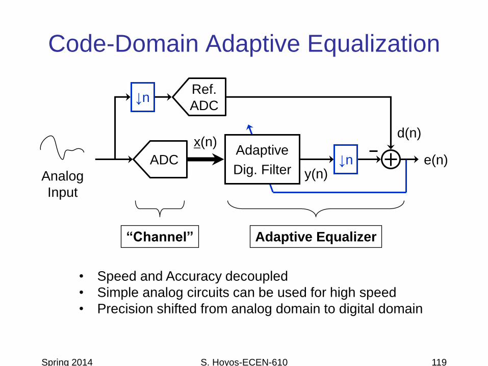
ADC
Analog
Input
Code-Domain Adaptive Equalization
Adaptive
Dig. Filter
“Channel” Adaptive Equalizer
• Speed and Accuracy decoupled
• Simple analog circuits can be used for high speed
• Precision shifted from analog domain to digital domain
x(n)
y(n)
d(n)
e(n)
↓nRef.
ADC
↓n

Spring 2014 S. Hoyos-ECEN-610 120
Multi-Stage ADC Gain Error
Accumulated Gain Mismatch
ADC with
gain error 4
321
3
21
2
1
1
1111 D
aaaD
aaD
aDDo
1-bit/stage
Ideal ADC 43218
1
4
1
2
11 DDDDDo

Spring 2014 S. Hoyos-ECEN-610 121
ADC Calibration: Filtering Approach
Analog
Input
ADCDigital
Correction
x(n)
y(n)
d(n)
e(n)
Ref. Path
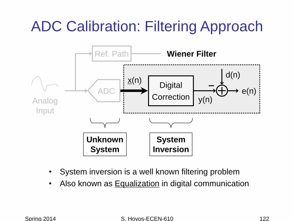
Spring 2014 S. Hoyos-ECEN-610 122
ADC
Analog
Input
Ref. Path
Digital
Correction
Unknown
System
System
Inversion
• System inversion is a well known filtering problem
• Also known as Equalization in digital communication
x(n)
y(n)
d(n)
e(n)
Wiener Filter
ADC Calibration: Filtering Approach

Spring 2014 S. Hoyos-ECEN-610 123
ADC
Analog
Input
Code-Domain Adaptive Equalization
Adaptive
Dig. Filter
“Channel” Adaptive Equalizer
• Speed and Accuracy decoupled
• Simple analog circuits can be used for high speed
• Precision shifted from analog domain to digital domain
x(n)
y(n)
d(n)
e(n)
↓nRef.
ADC
↓n
Spring 2014 S. Hoyos-ECEN-610 124
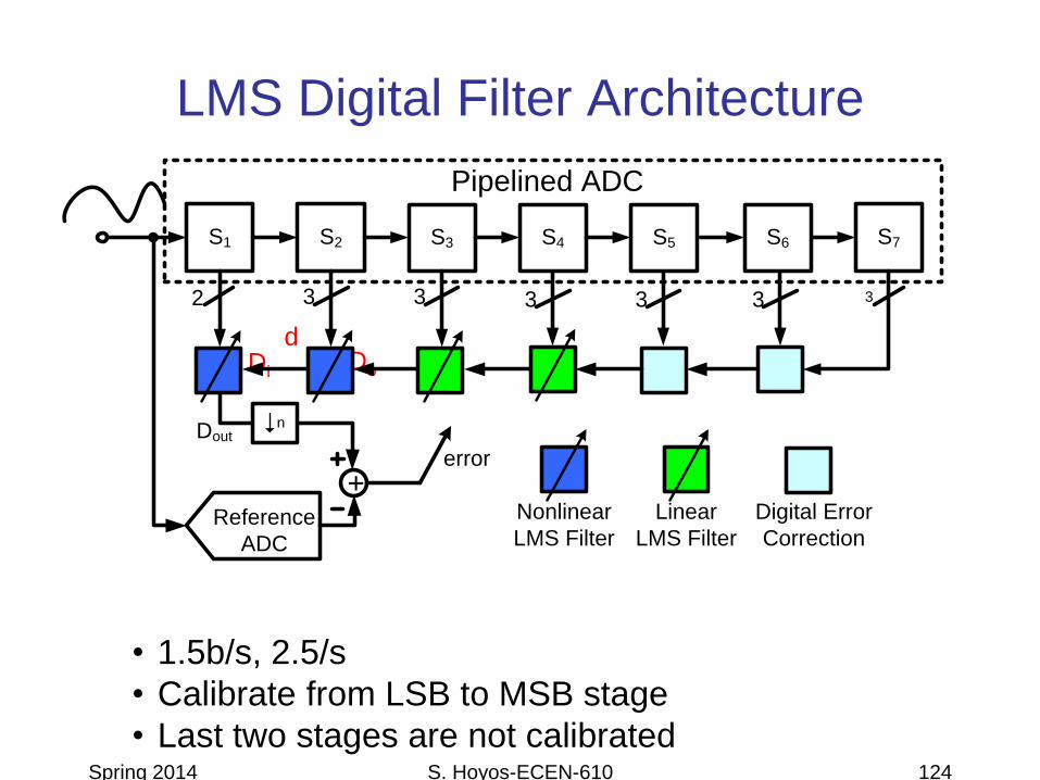
• 1.5b/s, 2.5/s
• Calibrate from LSB to MSB stage
• Last two stages are not calibrated
LMS Digital Filter Architecture
Do
dDi
S1 S2 S7
2 3 3
S3 S4 S5 S6
3 3 3 3
+
n
error
Dout
Pipelined ADC
Nonlinear
LMS Filter
Digital Error
Correction
Linear
LMS FilterReference
ADC

Spring 2014 S. Hoyos-ECEN-610 125
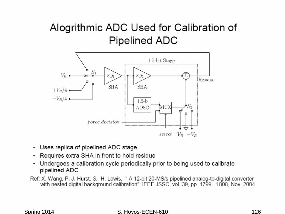
Spring 2014 S. Hoyos-ECEN-610 126

Spring 2014 S. Hoyos-ECEN-610 127

Spring 2014 S. Hoyos-ECEN-610 128

Spring 2014 S. Hoyos-ECEN-610 129

Spring 2014 S. Hoyos-ECEN-610 130
Spring 2014 S. Hoyos-ECEN-610 131

Spring 2014 S. Hoyos-ECEN-610 132

Spring 2014 S. Hoyos-ECEN-610 133

Spring 2014 S. Hoyos-ECEN-610 134
Spring 2014 S. Hoyos-ECEN-610 135

Spring 2014 S. Hoyos-ECEN-610 136
Spring 2014 S. Hoyos-ECEN-610 137
Spring 2014 S. Hoyos-ECEN-610 138

Spring 2014 S. Hoyos-ECEN-610 139

Spring 2014 S. Hoyos-ECEN-610 140

Spring 2014 S. Hoyos-ECEN-610 141

Spring 2014 S. Hoyos-ECEN-610 142
Spring 2014 S. Hoyos-ECEN-610 143

Spring 2014 S. Hoyos-ECEN-610 144

Spring 2014 S. Hoyos-ECEN-610 145

Spring 2014 S. Hoyos-ECEN-610 146
Spring 2014 S. Hoyos-ECEN-610 147
References
1. S. H. Lewis et al., JSSC, vol. 27, pp. 351-358, issue 3, 1992.
2. S. Sutarja et al., JSSC, vol. 23, pp. 1316-1323, issue 6, 1988.
3. B.-S. Song et al., JSSC, vol. 23, pp. 1324-1333, issue 6, 1988.
4. Y.-M. Lin et al., JSSC, vol. 26, pp. 628-636, issue 4, 1991.
5. A. N. Karanicolas et al., JSSC, vol. 28, pp. 1207-1215, issue 12, 1993.
6. K. Sone et al., JSSC, vol. 28, pp. 1180-1186, issue 12, 1993.
7. J. Wu et al., ISCAS, 1994, pp. 461-464 vol.5.
8. T.-H. Shu et al., JSSC, vol. 30, pp. 443-452, issue 4, 1995.
9. T. B. Cho et al., JSSC, vol. 30, pp. 166-172, issue 3, 1995.
10.P. C. Yu et al., JSSC, vol. 31, pp. 1854-1861, issue 12, 1996.
11.D. W. Cline et al., JSSC, vol. 31, pp. 294-303, issue 3, 1996.
12.L. A. Singer et al., VLSI, 1996, pp. 94-95.
13.S.-U. Kwak et al., JSSC, vol. 32, pp. 1866-1875, issue 12, 1997.
14.K. Y. Kim et al., JSSC, vol. 32, pp. 302-311, issue 3, 1997.
15.J. M. Ingino et al., JSSC, vol. 33, pp. 1920-1931, issue 12, 1998.

Spring 2014 S. Hoyos-ECEN-610 148
References
16. I. E. Opris et al., JSSC, vol. 33, pp. 1898-1903, issue 12, 1998.
17. I. Mehr et al., JSSC, vol. 35, pp. 318-325, issue 3, 2000.
18.D. Miyazaki et al., ISSCC, 2002, pp. 174-175, 458.
19.B.-M. Min et al., JSSC, vol. 38, pp. 2031-2039, issue 12, 2003.
20.B. Murmann et al., JSSC, vol. 38, pp. 2040-2050, issue 12, 2003.
21.X. Wang et al., CICC, 2003, pp. 409-412.
22.J. Li et al., CICC, 2003, pp. 413-416.
23.Y. Chiu et al., JSSC, vol. 39, pp. 2139-2151, issue 12, 2004.
24.E. Siragusa et al., JSSC, vol. 39, pp. 2126-2138, issue 12, 2004.
25.C. R. Grace et al., ISSCC, 2004, pp. 460-461, 539.