Embed Size (px)
Citation preview

Prof. Dr. Qiuting HuangIntegrated Systems Laboratory
Electronic Circuits
5. Instrumentation Amplifier

Precise amplification of weak sensor signals in the presence of distortion and noise, typically at microvolt level
High input impedance Internal feedback to achieve desired functionality Selectable gain, typically 𝐺𝐺 = 10, 100, 1000 Quality of InAmps determined by Common mode rejection ratio (CMRR) Voltage offset Noise
Application example: ECG
ETH 2Integrated Systems Laboratory
Characteristics of Instrumentation Amplifiers
and sensor front-end

Voltage difference amplifier Amplifies the difference signal with a precise gain Suppresses distortion (common mode signals) Presents the same impedance at both input terminals
Differential gain must be equal for both input branches
Set 𝑅𝑅1 = 𝑅𝑅3, 𝑅𝑅2 = 𝑅𝑅4 to equally load both input branches
ETH 3Integrated Systems Laboratory
Basic Instrumentation Amplifier
with 𝑉𝑉i+ = 0,
with 𝑉𝑉i− = 0,
𝑉𝑉o = −𝑅𝑅4𝑅𝑅3
𝑉𝑉i−
𝑉𝑉o =𝑅𝑅2
𝑅𝑅1 + 𝑅𝑅2�𝑅𝑅3 + 𝑅𝑅4𝑅𝑅3
𝑉𝑉i+
𝑉𝑉o =𝑅𝑅2 𝑅𝑅3 + 𝑅𝑅4𝑅𝑅3(𝑅𝑅1+𝑅𝑅2)
𝑉𝑉i+ −𝑅𝑅4𝑅𝑅3
𝑉𝑉i− =𝑅𝑅2𝑅𝑅1
1 + 𝑅𝑅4𝑅𝑅3
1 + 𝑅𝑅2𝑅𝑅1
𝑉𝑉i+ −𝑅𝑅4𝑅𝑅3
𝑉𝑉i−
superposition principle:
𝑉𝑉o = 𝐺𝐺 � 𝑉𝑉i+ − 𝐺𝐺 � 𝑉𝑉i− 𝐺𝐺 =𝑅𝑅2𝑅𝑅1
=𝑅𝑅4𝑅𝑅3
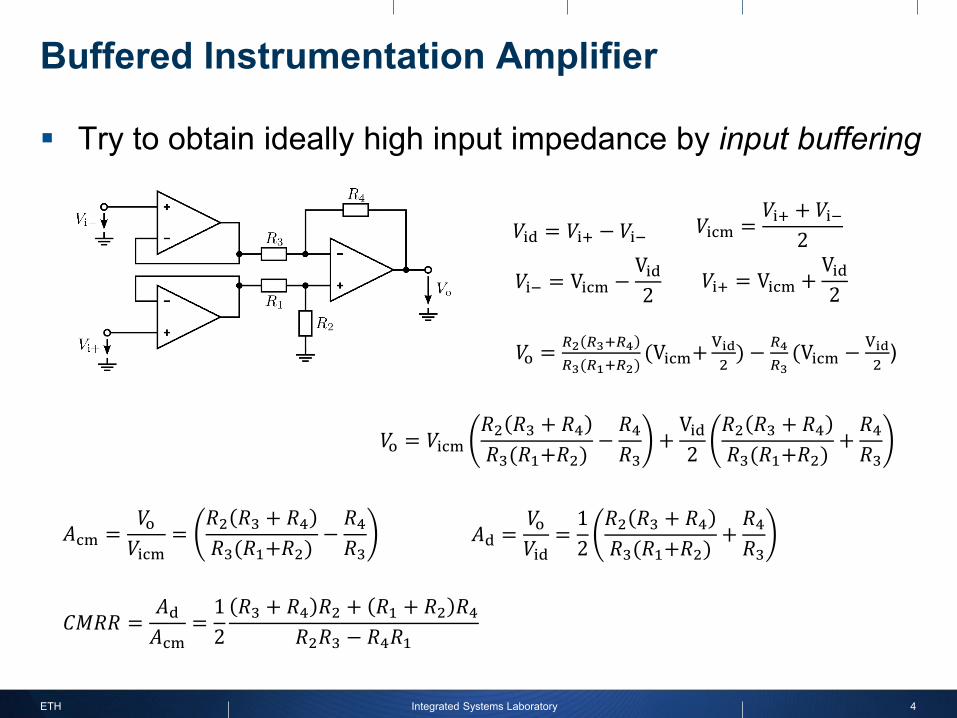
Try to obtain ideally high input impedance by input buffering
ETH 4Integrated Systems Laboratory
Buffered Instrumentation Amplifier
𝑉𝑉id = 𝑉𝑉i+ − 𝑉𝑉i− 𝑉𝑉icm =𝑉𝑉i+ + 𝑉𝑉i−
2
𝑉𝑉i− = Vicm −Vid2
𝑉𝑉i+ = Vicm +Vid2
𝑉𝑉o = 𝑅𝑅2 𝑅𝑅3+𝑅𝑅4𝑅𝑅3(𝑅𝑅1+𝑅𝑅2)
(Vicm+ Vid2
) − 𝑅𝑅4𝑅𝑅3
(Vicm − Vid2
)
𝑉𝑉o = 𝑉𝑉icm𝑅𝑅2 𝑅𝑅3 + 𝑅𝑅4𝑅𝑅3(𝑅𝑅1+𝑅𝑅2)
−𝑅𝑅4𝑅𝑅3
+Vid2
𝑅𝑅2 𝑅𝑅3 + 𝑅𝑅4𝑅𝑅3(𝑅𝑅1+𝑅𝑅2)
+𝑅𝑅4𝑅𝑅3
𝐴𝐴cm =𝑉𝑉o𝑉𝑉icm
=𝑅𝑅2 𝑅𝑅3 + 𝑅𝑅4𝑅𝑅3(𝑅𝑅1+𝑅𝑅2)
−𝑅𝑅4𝑅𝑅3
𝐴𝐴d =𝑉𝑉o𝑉𝑉id
=12
𝑅𝑅2 𝑅𝑅3 + 𝑅𝑅4𝑅𝑅3(𝑅𝑅1+𝑅𝑅2)
+𝑅𝑅4𝑅𝑅3
𝐶𝐶𝐶𝐶𝑅𝑅𝑅𝑅 =𝐴𝐴d𝐴𝐴cm
=12𝑅𝑅3 + 𝑅𝑅4 𝑅𝑅2 + 𝑅𝑅1 + 𝑅𝑅2 𝑅𝑅4
𝑅𝑅2𝑅𝑅3 − 𝑅𝑅4𝑅𝑅1

ETH 5Integrated Systems Laboratory
InAmp - Common Mode Rejection and Precision
Resistor manufacturing tolerance 𝑅𝑅1 = 𝑅𝑅 1 + 𝜖𝜖
Example:
𝑅𝑅2 = 𝑅𝑅3 = 𝑅𝑅4 = 𝑅𝑅
𝐶𝐶𝐶𝐶𝑅𝑅𝑅𝑅 =12𝑅𝑅2
𝑅𝑅2(3 + 1 + 𝜖𝜖)(1 − 1 − 𝜖𝜖)
≈2𝜖𝜖
𝜖𝜖 = 1% ⇒ 𝐶𝐶𝐶𝐶𝑅𝑅𝑅𝑅 = 200 = 46 dB
to achieve 𝐶𝐶𝐶𝐶𝑅𝑅𝑅𝑅 ≥ 100𝑑𝑑𝑑𝑑: 𝜖𝜖 ≤ 0.002%
𝐶𝐶𝐶𝐶𝑅𝑅𝑅𝑅 =12𝑅𝑅3 + 𝑅𝑅4 𝑅𝑅2 + 𝑅𝑅1 + 𝑅𝑅2 𝑅𝑅4
𝑅𝑅2𝑅𝑅3 − 𝑅𝑅4𝑅𝑅1
𝑅𝑅2𝑅𝑅1
=𝑅𝑅4𝑅𝑅3
leads to infinite CMRR, but can not be realized with real-world resistorsdue to manufacturing deviations
𝜖𝜖 ≪ 1

ETH 6Integrated Systems Laboratory
Instrumentation Amplifier – Input Stage Gain
Differential gain of input stage:
𝐴𝐴B =𝑉𝑉Bd𝑉𝑉id
=𝑉𝑉B+ − 𝑉𝑉B−𝑉𝑉i+ − 𝑉𝑉i−
= 1 +𝑅𝑅5 + 𝑅𝑅6𝑅𝑅7
𝑅𝑅6 = 𝑅𝑅5 ⇒ 𝐴𝐴B = 1 +2𝑅𝑅5𝑅𝑅7
CMRR increased by factor of 𝐴𝐴B
𝐶𝐶𝐶𝐶𝑅𝑅𝑅𝑅 =𝐴𝐴𝐴d𝐴𝐴cm
= 𝐴𝐴B𝐴𝐴d𝐴𝐴cm
𝐴𝐴𝐴d =𝑉𝑉o𝑉𝑉id
=𝐴𝐴B2
𝑅𝑅2 𝑅𝑅3 + 𝑅𝑅4𝑅𝑅3(𝑅𝑅1+𝑅𝑅2)
+𝑅𝑅4𝑅𝑅3
𝑅𝑅1 = 𝑅𝑅3, 𝑅𝑅2= 𝑅𝑅4
𝐴𝐴𝐴d =𝑅𝑅2𝑅𝑅1𝐴𝐴B
Total differential gain:
𝑉𝑉id = 𝑉𝑉i+ − 𝑉𝑉i−
𝑉𝑉Bd = 𝑉𝑉B+ − 𝑉𝑉B−
Differential input
Differential output of
the input stage
Common mode gain of input stage:
𝑉𝑉i+ = 𝑉𝑉i− = 𝑉𝑉CM ⇒ ideal op-amp 𝑉𝑉d = 0⇒ no current flowing through 𝑅𝑅7, northrough 𝑅𝑅5 and 𝑅𝑅6 ⇒ 𝑉𝑉B+ = 𝑉𝑉CM = 𝑉𝑉B−
𝐴𝐴cm,B =𝑉𝑉B+ + 𝑉𝑉B−𝑉𝑉i+ + 𝑉𝑉i−
= 1
Total common mode gain:
𝐴𝐴cm = 𝐴𝐴cm,B𝑅𝑅2 𝑅𝑅3 + 𝑅𝑅4𝑅𝑅3(𝑅𝑅1+𝑅𝑅2)
−𝑅𝑅4𝑅𝑅3
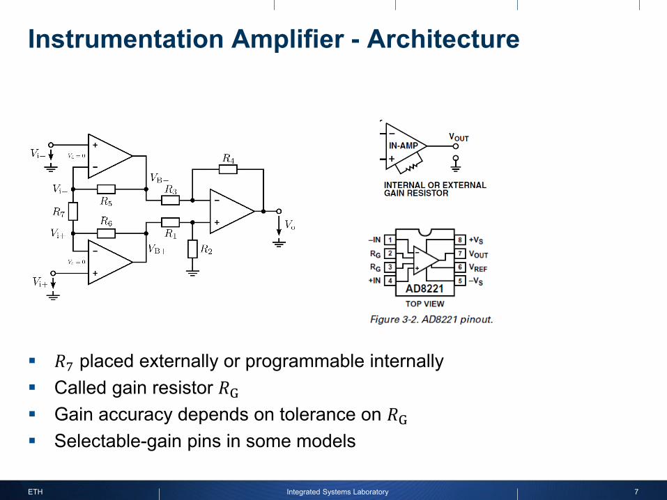
𝑅𝑅7 placed externally or programmable internally Called gain resistor 𝑅𝑅G Gain accuracy depends on tolerance on 𝑅𝑅G Selectable-gain pins in some models
ETH 7Integrated Systems Laboratory
Instrumentation Amplifier - Architecture

Offset has its origin in small, production-related deviations of integrated devices from their nominal values
ETH 8Integrated Systems Laboratory
Voltage Offsets in Differential Amplifiers
For symmetry 𝐼𝐼D1 = 𝐼𝐼D2 ⇒ 𝑉𝑉TH1 =𝑉𝑉TH2 is necessary
But: 𝑉𝑉TH1 = 𝑉𝑉TH,𝑉𝑉TH2 = 𝑉𝑉TH + 𝑉𝑉ϵ 𝑉𝑉𝜖𝜖 caused by production deviation An offset voltage 𝑉𝑉os = 𝑉𝑉𝜖𝜖 can be
added externally in order to restore symmetry
Then 𝑉𝑉TH1 = 𝑉𝑉TH = 𝑉𝑉TH2 + 𝑉𝑉ϵ − 𝑉𝑉os
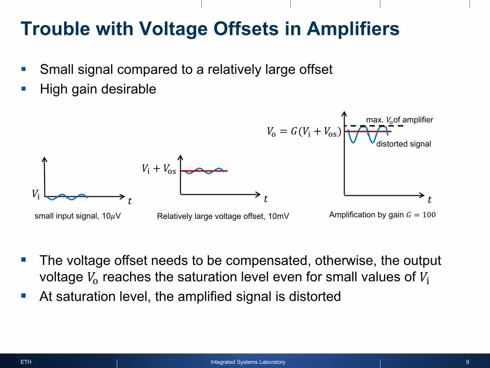
Small signal compared to a relatively large offset High gain desirable
ETH 9Integrated Systems Laboratory
Trouble with Voltage Offsets in Amplifiers
𝑉𝑉i 𝑡𝑡small input signal, 10𝜇𝜇V
𝑉𝑉i + 𝑉𝑉os
𝑡𝑡Relatively large voltage offset, 10mV
The voltage offset needs to be compensated, otherwise, the output voltage 𝑉𝑉o reaches the saturation level even for small values of 𝑉𝑉i
At saturation level, the amplified signal is distorted
𝑉𝑉o = 𝐺𝐺(𝑉𝑉i + 𝑉𝑉os)
𝑡𝑡Amplification by gain 𝐺𝐺 = 100
max. 𝑉𝑉oof amplifier
distorted signal

ETH 10Integrated Systems Laboratory
Inverting Amplifier with DC Offset Voltage
If 𝐴𝐴o → ∞ then 𝑉𝑉d → 0, 𝑉𝑉d′ = 𝑉𝑉os
KCL: 𝑉𝑉o−𝑉𝑉os𝑅𝑅2
= −𝑉𝑉𝑖𝑖−𝑉𝑉os𝑅𝑅1
⇒ 𝑉𝑉o = −𝑅𝑅2𝑅𝑅1𝑉𝑉i + 1 + 𝑅𝑅2
𝑅𝑅1𝑉𝑉os
Offset term can become problematic if |𝑉𝑉i| ≈ |𝑉𝑉os|
sensor applications
offset term

Offsets 𝑉𝑉os1, 𝑉𝑉os2 can be seen as part of the input signals 𝑉𝑉i+ and 𝑉𝑉i− 𝑉𝑉os1, 𝑉𝑉os2 see the same gain as input signal
𝑉𝑉o𝑠𝑠 = 𝑉𝑉os2 − 𝑉𝑉os1 1 + 𝑅𝑅5+𝑅𝑅6𝑅𝑅7
Offsets can be modeled as uncorrelated random variables. This means that 𝑉𝑉os2 − 𝑉𝑉os1 is also a random variable, with twice the variance
ETH 11Integrated Systems Laboratory
Input Stage Voltage Offset

Offset trimming (“nulling”) by external components in op-amp
If such compensation methods are not appropriate, amplifiers based on signal chopping can be used chopper amplifiers
ETH 12Integrated Systems Laboratory
Voltage Offset Compensation in Integrated Amplifiers
741 op-amp
(as used in thelaboratory)

ETH 13Integrated Systems Laboratory
Chopping Principle
𝑓𝑓s
𝑓𝑓s𝑓𝑓c𝑓𝑓c + 𝑓𝑓s𝑓𝑓c − 𝑓𝑓s
𝑉𝑉i+
𝑉𝑉i−𝑓𝑓
𝐹𝐹
𝐹𝐹𝑉𝑉i+ =𝐴𝐴2𝛿𝛿(𝑓𝑓 − 𝑓𝑓s)
𝑉𝑉i+ = 𝐴𝐴cos 2𝜋𝜋𝑡𝑡𝑓𝑓s Fourier transform,
negative frequencies
neglected for simplicity
𝑉𝑉i+ = 𝐴𝐴cos 2𝜋𝜋𝑡𝑡𝑓𝑓s + 𝑉𝑉os
𝐹𝐹𝑉𝑉i+ =𝐴𝐴2𝛿𝛿 𝑓𝑓 − 𝑓𝑓s + 𝑉𝑉os𝛿𝛿(𝑓𝑓)
𝑉𝑉i+ = cos 2𝜋𝜋𝑡𝑡𝑓𝑓c 𝐴𝐴cos 2𝜋𝜋𝑡𝑡𝑓𝑓s + 𝑉𝑉os
𝐹𝐹𝑉𝑉i+ =𝐴𝐴4𝛿𝛿 𝑓𝑓 − (𝑓𝑓c + 𝑓𝑓s) +
𝐴𝐴4𝛿𝛿 𝑓𝑓 − (𝑓𝑓c − 𝑓𝑓s) + 𝑉𝑉os𝛿𝛿(𝑓𝑓)
𝐹𝐹c =12𝛿𝛿 𝑓𝑓 − 𝑓𝑓c𝑠𝑠c = cos 2𝜋𝜋𝑡𝑡𝑓𝑓c
𝑉𝑉o+
𝑉𝑉o−
𝑓𝑓s 𝑓𝑓
𝐹𝐹
𝑓𝑓
𝐹𝐹
𝐺𝐺
𝑉𝑉os𝑉𝑉i+ 𝑉𝑉o++ −
𝐺𝐺
𝑉𝑉os𝑠𝑠c
𝑉𝑉o++ −𝑉𝑉i+
𝐺𝐺
𝑉𝑉i+ =𝐴𝐴2
[cos 2𝜋𝜋𝑡𝑡(𝑓𝑓s−𝑓𝑓c) + cos 2𝜋𝜋𝑡𝑡(𝑓𝑓s+𝑓𝑓c) ] + 𝑉𝑉os

The output of the chopper amplifier is finally low pass filtered in order to suppress out of band frequencies
ETH 14Integrated Systems Laboratory
Chopping Principle
𝐹𝐹o+ =𝐺𝐺𝐴𝐴4𝛿𝛿 𝑓𝑓 − 𝑓𝑓s
𝑠𝑠c
𝑉𝑉o++ −𝑉𝑉i+
𝑉𝑉os
𝐺𝐺 LPF
𝑠𝑠c𝑉𝑉𝐴i+
𝑉𝑉o+ =𝐺𝐺𝐴𝐴2
cos 2𝜋𝜋𝑡𝑡𝑓𝑓s + 𝑉𝑉os 𝐺𝐺cos 2𝜋𝜋𝑓𝑓c
+ 𝐺𝐺𝐺𝐺4
cos(2𝜋𝜋𝑡𝑡(𝑓𝑓s + 2𝑓𝑓c)) + 𝐺𝐺𝐺𝐺4
cos(2𝜋𝜋𝑡𝑡(𝑓𝑓s − 2𝑓𝑓c))
𝐹𝐹o+ =𝐺𝐺𝐴𝐴4𝛿𝛿 𝑓𝑓 − 𝑓𝑓s +
𝐺𝐺𝑉𝑉os2
𝛿𝛿 𝑓𝑓 − 𝑓𝑓c +𝐺𝐺𝐴𝐴8𝛿𝛿(𝑓𝑓 − 𝑓𝑓s − 2𝑓𝑓c) +
𝐺𝐺𝐴𝐴8𝛿𝛿(𝑓𝑓 + 𝑓𝑓s − 2𝑓𝑓c)
𝑠𝑠c𝑉𝑉o+
+ −𝑉𝑉i+
𝑉𝑉os
𝐺𝐺
𝑠𝑠c
𝑓𝑓𝑓𝑓s 𝑓𝑓c
𝐹𝐹
2𝑓𝑓c
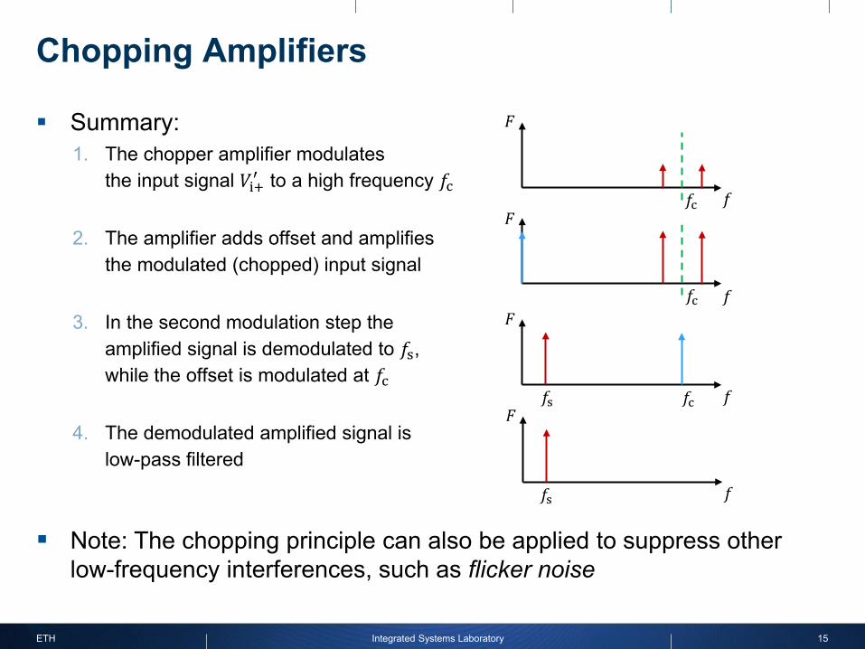
Summary:1. The chopper amplifier modulates
the input signal 𝑉𝑉i+′ to a high frequency 𝑓𝑓c
2. The amplifier adds offset and amplifies the modulated (chopped) input signal
3. In the second modulation step the amplified signal is demodulated to 𝑓𝑓s, while the offset is modulated at 𝑓𝑓c
4. The demodulated amplified signal is low-pass filtered
ETH 15Integrated Systems Laboratory
Chopping Amplifiers
𝑓𝑓
𝐹𝐹
Note: The chopping principle can also be applied to suppress other low-frequency interferences, such as flicker noise
𝑓𝑓c
𝑓𝑓
𝐹𝐹
𝑓𝑓c
𝑓𝑓
𝐹𝐹
𝑓𝑓s 𝑓𝑓c
𝑓𝑓
𝐹𝐹
𝑓𝑓s


![Verilog for Sequential Circuits - ETH Zurich · Adapted from Digital Design and Computer Architecture, ... module flop_sr (input clk, input ... [6:0] segments);](https://img.dokumen.tips/doc/110x75/5b37738a7f8b9abd438c36d2/verilog-for-sequential-circuits-eth-adapted-from-digital-design-and-computer.jpg)