Embed Size (px)
Citation preview

Prof. Dr. Qiuting HuangIntegrated Systems Laboratory
Electronic Circuits
1. Introduction

ETH 2Integrated Systems Laboratory
Electronic Systems
Electrical and electronic equipmentis indispensable in our daily lives

ETH 3Integrated Systems Laboratory
Electronics Industry Overview
World Production per Sector
• Electronics industry: ~1300 Billion Euro• Key driver for global economic growth
• Responsible for ~10% of global GDP (incl. service providers)
More than just consumer electronics
Automotive9%
HomeAppliances
6%
Telecoms21%
Audio/Video13%
Industrial &Medical
17%
Data Processing24%
Aero / Defense& Security
10%

ETH 4Integrated Systems Laboratory
Progress in Electronics and Enabled Applications
Improvements in electronics have drastically changed our daily lives
in the past 50 years.

ETH 5Integrated Systems Laboratory
Applications of Transistor Circuits
PCB with operational amplifiers to contact a temperature sensor to a microcontroller board.
Mixed analog and digital integrated circuit for biomedical applications developed at the IIS.
Backpack with solar collectors for hiking.

Miniaturized Device for Monitoring Oxygen Saturation
6ETH Integrated Systems Laboratory

Resistor
Capacitor
Inductor
ETH 7Integrated Systems Laboratory
Review of Passive Components
Range (SMD): 1 pF − 300 𝜇𝜇F
Range (SMD): 0.01 Ω − 10 MΩ
Range (SMD): 1 nH − 10 mH
𝑉𝑉R = 𝑅𝑅𝐼𝐼R
𝐼𝐼C = 𝐶𝐶dd𝑡𝑡𝑉𝑉C
𝑉𝑉L = 𝐿𝐿dd𝑡𝑡𝐼𝐼L
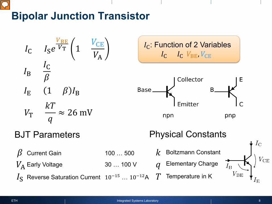
𝐼𝐼C = 𝐼𝐼S𝑒𝑒𝑉𝑉BE𝑉𝑉T 1 +
𝑉𝑉CE𝑉𝑉A
BJT Parameters
ETH 8Integrated Systems Laboratory
Bipolar Junction Transistor
𝐼𝐼B =𝐼𝐼C𝛽𝛽
𝐼𝐼E = 1 + 𝛽𝛽 𝐼𝐼B
𝛽𝛽
𝐼𝐼S𝑉𝑉A
𝑉𝑉T =𝑘𝑘𝑘𝑘𝑞𝑞≈ 26 mV
Current Gain
Early Voltage
Reverse Saturation Current
Physical Constants
𝑘𝑘𝑞𝑞𝑘𝑘
Boltzmann Constant
Elementary Charge
Temperature in K
𝐼𝐼C: Function of 2 Variables𝐼𝐼C = 𝐼𝐼C(𝑉𝑉BE,𝑉𝑉CE)
100 … 500
30 … 100 V
10−15 … 10−12A

In general: 𝐼𝐼C = 𝐼𝐼C(𝑉𝑉BE,𝑉𝑉CE) function of 2 variables
𝐼𝐼C(𝑉𝑉BE,𝑉𝑉CE) = 𝐼𝐼S𝑒𝑒𝑉𝑉BE𝑉𝑉T (1 + 𝑉𝑉CE
𝑉𝑉A)
ETH 9Integrated Systems Laboratory
2-Dimensional I/V Characteristic
𝑉𝑉BE fixed: 𝐼𝐼C(𝑉𝑉CE)𝑉𝑉CE fixed: 𝐼𝐼C(𝑉𝑉BE)
𝑉𝑉BE [V]
[mA
]
[mA
]
𝑉𝑉BE1
𝑉𝑉BE2
𝑉𝑉BE3
𝑉𝑉BE4
𝑉𝑉CE [V]
Saturation
Forward Active

ETH 10Integrated Systems Laboratory
Analytical Calculation of Transistor Circuits
𝐼𝐼C = 𝐼𝐼S𝑒𝑒𝑉𝑉BE𝑉𝑉T (1 +
𝑉𝑉CE𝑉𝑉A
)
𝐼𝐼C =𝛽𝛽
𝛽𝛽 + 1𝐼𝐼E ≈ 𝐼𝐼E =
𝑉𝑉E𝑅𝑅E
𝑉𝑉out = 𝑉𝑉CC − 𝐼𝐼C𝑅𝑅L
𝑉𝑉E𝑅𝑅E
− 𝐼𝐼S𝑒𝑒𝑉𝑉in−𝑉𝑉E−𝑉𝑉EE
𝑉𝑉T = 0
Transcendental equation:No analytical solution
≈ 𝐼𝐼S𝑒𝑒𝑉𝑉BE𝑉𝑉T = 𝐼𝐼S𝑒𝑒
𝑉𝑉in−𝑉𝑉E−𝑉𝑉EE𝑉𝑉T
𝛽𝛽 ≫ 1
𝑉𝑉A ≫ 𝑉𝑉CE

ETH 11Integrated Systems Laboratory
Graphical Solution
𝐼𝐼E =𝑉𝑉E𝑅𝑅E
≈ 𝐼𝐼S𝑒𝑒𝑉𝑉in−𝑉𝑉E−𝑉𝑉EE
𝑉𝑉T
Solution 1: Graphical Solution
𝐼𝐼𝐶𝐶
𝐼𝐼C(𝑉𝑉in,1)
𝐼𝐼C
𝑉𝑉E
𝐼𝐼C(𝑉𝑉in,2)
𝐼𝐼C(𝑉𝑉in,3)
𝐼𝐼C(𝑉𝑉in,4)
𝐼𝐼E =𝑉𝑉E𝑅𝑅E

ETH 12Integrated Systems Laboratory
Small Signal EquivalentSolution 2: Small Signal Equivalent• Set 𝑉𝑉CC = 𝑉𝑉EE = 0
𝑣𝑣E𝑅𝑅E
= 𝑔𝑔m(𝑣𝑣in − 𝑣𝑣E)
𝑖𝑖C =𝛽𝛽
𝛽𝛽 + 1𝑣𝑣E𝑅𝑅E
≈𝑣𝑣E𝑅𝑅E
𝑣𝑣out = −𝑖𝑖C𝑅𝑅L ≈ −𝑣𝑣E𝑅𝑅E
𝑅𝑅L = −𝒈𝒈𝐦𝐦𝑹𝑹𝐋𝐋
𝟏𝟏 + 𝒈𝒈𝐦𝐦𝑹𝑹𝐄𝐄𝒗𝒗𝐢𝐢𝐢𝐢
𝑣𝑣E =𝑔𝑔m𝑅𝑅E
1 + 𝑔𝑔m𝑅𝑅E𝑣𝑣in
𝑔𝑔m: transconductance
• Approximate 𝐼𝐼C = 𝐼𝐼S𝑒𝑒𝑉𝑉BE𝑉𝑉T for small
signals around the operating point as 𝑖𝑖C = d𝐼𝐼C
d𝑉𝑉BE(𝑣𝑣in − 𝑣𝑣E) = 𝑔𝑔m(𝑣𝑣in − 𝑣𝑣E)

ETH 13Integrated Systems Laboratory
The Transistor Amplifier
𝐼𝐼C
𝑉𝑉CE
Operating
Point
𝐼𝐼C
𝑉𝑉BE
Gain depends on theoperating point

ETH 14Integrated Systems Laboratory
The Transistor Amplifier
𝐼𝐼C
𝑉𝑉CE
Operating
Point
𝐼𝐼C
𝑉𝑉BE
Gain depends on theoperating point

𝐼𝐼C
𝑉𝑉CE
Operating
Point
𝐼𝐼C
𝑉𝑉BE
ETH 15Integrated Systems Laboratory
The Transistor Amplifier
Gain depends on theoperating point

𝑉𝑉CE
𝐼𝐼C
𝑉𝑉BE
ETH 16Integrated Systems Laboratory
The Transistor Amplifier
𝐼𝐼C
Gain depends on theoperating point

ETH 17Integrated Systems Laboratory
Transistor Amplifier – Nonlinear Distortion
Operating
Point
𝐼𝐼C𝐼𝐼C
𝑉𝑉CE𝑉𝑉BE𝑉𝑉BE2
𝑉𝑉BE3
𝑉𝑉BE1
𝑉𝑉BE2
𝑉𝑉BE3
𝑉𝑉BE1

ETH 18Integrated Systems Laboratory
BJT – Small Signal Parameters
𝐼𝐼C
𝑉𝑉BE
d𝐼𝐼C
d𝑉𝑉BE
𝑔𝑔m
𝑔𝑔𝜋𝜋
𝑔𝑔o𝐼𝐼C
𝑉𝑉CE
=𝐼𝐼S𝑉𝑉A𝑒𝑒𝑉𝑉BE𝑉𝑉T
𝐼𝐼C = 𝛽𝛽𝐼𝐼B
=𝜕𝜕
𝜕𝜕𝑉𝑉BE𝐼𝐼S 𝑒𝑒
𝑉𝑉BE𝑉𝑉T 1 +
𝑉𝑉CE𝑉𝑉A
=𝐼𝐼C𝑉𝑉T
=𝜕𝜕𝐼𝐼C𝜕𝜕𝑉𝑉BE
=𝑔𝑔m𝛽𝛽
=1𝛽𝛽𝜕𝜕𝐼𝐼C𝜕𝜕𝑉𝑉BE
=𝜕𝜕𝐼𝐼B𝜕𝜕𝑉𝑉BE
=𝐼𝐼C
𝑉𝑉A + 𝑉𝑉CE
=𝜕𝜕𝐼𝐼C𝜕𝜕𝑉𝑉CE
=𝜕𝜕
𝜕𝜕𝑉𝑉CE𝐼𝐼S 𝑒𝑒
𝑉𝑉BE𝑉𝑉T 1 +
𝑉𝑉CE𝑉𝑉A

ETH 19Integrated Systems Laboratory
BJT – Small Signal Equivalent
𝑟𝑟𝜋𝜋 =1𝑔𝑔𝜋𝜋
=𝛽𝛽𝑔𝑔m
𝑟𝑟o =1𝑔𝑔o
=𝑉𝑉A + 𝑉𝑉CE
𝐼𝐼C≈𝑉𝑉A𝐼𝐼C
𝑉𝑉A ≫ 𝑉𝑉CE
𝑔𝑔m =𝐼𝐼C𝑉𝑉T

20Integrated Systems Laboratory
Small Signal Equivalent – Numerical Example
𝑟𝑟𝜋𝜋 =𝛽𝛽𝑔𝑔m
=
𝑔𝑔m =𝐼𝐼C𝑉𝑉T
=4.6 S
0.15 S0. 77 S
3.3 kΩ649 Ω109 Ω
ETH

ETH 21Integrated Systems Laboratory
Example: Common Emitter Amplifier

ETH 22Integrated Systems Laboratory
Example: Common Emitter Amplifier

ETH 23Integrated Systems Laboratory
Example: Common Emitter AmplifierLarge Signal: Replace the linear part by its Thévenin equivalent

ETH 24Integrated Systems Laboratory
Example: Common Emitter AmplifierLarge Signal: Replace the linear part by its Thévenin equivalent
VTHE =VCCRB2
RB1 + RB2
RTHE =RB1RB2
RB1 + RB2

ETH 25Integrated Systems Laboratory
Example: Common Emitter AmplifierLarge Signal: Replace the linear part by its Thévenin equivalent
𝑉𝑉BE = 𝑉𝑉THE − 𝐼𝐼B𝑅𝑅THE = 𝑉𝑉T ln𝛽𝛽𝐼𝐼B𝐼𝐼S
VTHE =VCCRB2
RB1 + RB2
RTHE =RB1RB2
RB1 + RB2
𝑉𝑉BE ≈ 0.7 V = 𝑉𝑉THE − 𝐼𝐼B𝑅𝑅THE
𝐼𝐼B =𝑉𝑉THE − 𝑉𝑉BE
𝑅𝑅THE
𝑰𝑰𝐁𝐁 =𝑽𝑽𝐂𝐂𝐂𝐂𝑹𝑹𝐁𝐁𝐁𝐁
𝑹𝑹𝐁𝐁𝟏𝟏 + 𝑹𝑹𝐁𝐁𝐁𝐁− 𝑽𝑽𝐁𝐁𝐄𝐄
𝑹𝑹𝐁𝐁𝟏𝟏 + 𝑹𝑹𝐁𝐁𝐁𝐁𝑹𝑹𝐁𝐁𝟏𝟏𝑹𝑹𝐁𝐁𝐁𝐁
𝑰𝑰𝐂𝐂 = 𝜷𝜷𝑰𝑰𝐁𝐁

ETH 26Integrated Systems Laboratory
Example: Common Emitter AmplifierSmall Signal

ETH 27Integrated Systems Laboratory
Example: Common Emitter Amplifier
𝑔𝑔m =𝐼𝐼C𝑉𝑉T
, 𝑟𝑟𝜋𝜋 =𝛽𝛽𝑔𝑔m
Small Signal
𝑟𝑟o =𝑉𝑉A𝐼𝐼C

ETH 28Integrated Systems Laboratory
Example: Common Emitter Amplifier
𝑔𝑔m =𝐼𝐼C𝑉𝑉T
, 𝑟𝑟𝜋𝜋 =𝛽𝛽𝑔𝑔m
Small Signal
𝑣𝑣out = −𝑔𝑔m𝑣𝑣in(𝑅𝑅L||𝑟𝑟o)
𝐴𝐴V =𝑣𝑣out𝑣𝑣in
= −𝑔𝑔m(𝑅𝑅L| 𝑟𝑟o ≈ −𝑔𝑔m𝑅𝑅L
𝑟𝑟o =𝑉𝑉A𝐼𝐼C
𝑅𝑅L ≪ 𝑟𝑟o

The voltage divider 𝑅𝑅B1,𝑅𝑅B2sets the bias voltage for the BJT.
𝑅𝑅E defines 𝐼𝐼E
𝑉𝑉B = 𝑉𝑉THE − 𝐼𝐼B𝑅𝑅THE ≈𝑉𝑉CC𝑅𝑅B2𝑅𝑅B1+𝑅𝑅B2
𝑉𝑉E = 𝑉𝑉B − 𝑉𝑉BE 𝐼𝐼C ≈ 𝐼𝐼E = 𝑉𝑉E
𝑅𝑅E
𝐼𝐼B = 𝐼𝐼C𝛽𝛽
ETH 29Integrated Systems Laboratory
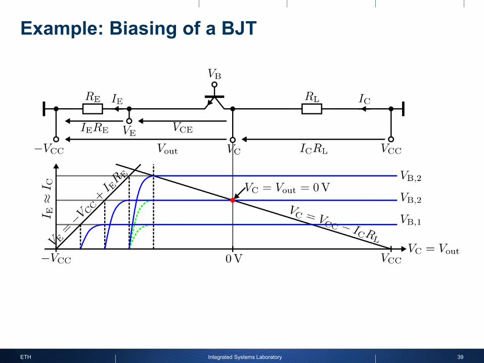
Biasing of a BJT
𝐼𝐼E ≈ 𝐼𝐼C
Large Signal

ETH 30Integrated Systems Laboratory
Example: Biasing of a BJT
Design the biasing network for𝑅𝑅L = 1kΩ, 𝛽𝛽 = 500, 𝑉𝑉CC= 5 V
What we would like to have: Output DC level: 𝑉𝑉out = 0 V Output signal swing: 𝑉𝑉swing = 2 V Transistor in active region, 𝑉𝑉BE ≈ 0.7 V
How large is 𝑉𝑉𝑅𝑅B2? What we know
𝐼𝐼C = 𝐼𝐼S𝑒𝑒𝑉𝑉BE𝑉𝑉T 1 + 𝑉𝑉CE
𝑉𝑉A= 𝐼𝐼𝑠𝑠𝑒𝑒
𝑉𝑉B−𝑉𝑉E𝑉𝑉T 1 + 𝑉𝑉C−𝑉𝑉E
𝑉𝑉A 𝑉𝑉C = 𝑉𝑉CC − 𝐼𝐼C𝑅𝑅L ≈ 𝑉𝑉CC − 𝐼𝐼E𝑅𝑅L,𝛽𝛽 ≫ 1 𝑉𝑉E = −𝑉𝑉CC + 𝑉𝑉𝑅𝑅E = −𝑉𝑉CC + 𝐼𝐼E𝑅𝑅E
𝑉𝑉CE,min = 0.2 V

Example: Biasing of a BJT
ETH 31Integrated Systems Laboratory

Example: Biasing of a BJT
ETH 32Integrated Systems Laboratory

Example: Biasing of a BJT
ETH 33Integrated Systems Laboratory

Example: Biasing of a BJT
ETH 34Integrated Systems Laboratory

Example: Biasing of a BJT
ETH 35Integrated Systems Laboratory

Example: Biasing of a BJT
ETH 36Integrated Systems Laboratory

Example: Biasing of a BJT
ETH 37Integrated Systems Laboratory

Example: Biasing of a BJT
ETH 38Integrated Systems Laboratory
Example: Biasing of a BJT
ETH 39Integrated Systems Laboratory

Example: Biasing of a BJT
ETH 40Integrated Systems Laboratory

Example: Biasing of a BJT
ETH 41Integrated Systems Laboratory
𝑉𝑉CE = 𝑉𝑉C − 𝑉𝑉E = 𝑉𝑉out + 𝑉𝑉cc − 𝑉𝑉swing − 𝑉𝑉𝑅𝑅E ≥ 𝑉𝑉CE,min𝑉𝑉𝑅𝑅E ≤ 𝑉𝑉CC + 𝑉𝑉out − 𝑉𝑉swing − 𝑉𝑉CE,min = 2.8 V𝑉𝑉𝑅𝑅B2 = 𝑉𝑉𝑅𝑅E + 𝑉𝑉BE = 3.5 V

Thevenin: 𝑉𝑉𝑅𝑅B2 = 𝑉𝑉THE − 𝐼𝐼B𝑅𝑅THE ≈ 𝑉𝑉THE
𝑉𝑉𝑅𝑅B2 ≈2𝑉𝑉CC𝑅𝑅B2𝑅𝑅B1+𝑅𝑅B2
⟹ 𝑅𝑅B2 =𝑉𝑉𝑅𝑅B2 𝑅𝑅B1+𝑅𝑅B2
2𝑉𝑉CC Choosing 𝑅𝑅B1 + 𝑅𝑅B2 = 10 kΩ
𝑅𝑅B2 = 𝟑𝟑.𝟓𝟓 𝐤𝐤𝐤𝐤, 𝑅𝑅B1 = 𝟔𝟔.𝟓𝟓 𝐤𝐤𝐤𝐤
𝑅𝑅E =𝑉𝑉𝑅𝑅E𝐼𝐼E
= 𝟓𝟓𝟔𝟔𝟓𝟓 𝐤𝐤 with 𝐼𝐼E ≈ 𝐼𝐼C = 𝑉𝑉CC−𝑉𝑉out𝑅𝑅L
ETH 42Integrated Systems Laboratory
Example: Biasing of a BJT
𝐼𝐼B =𝑉𝑉THE − 𝑉𝑉BE
𝑅𝑅THE + 1 + 𝛽𝛽 𝑅𝑅E= 9.9 𝜇𝜇A 𝑉𝑉𝑅𝑅B2 = 𝑉𝑉THE − 𝐼𝐼B𝑅𝑅THE = 3.48 V
𝐼𝐼E
Check the result: desired is𝐼𝐼B = 𝐼𝐼C
𝛽𝛽= 10 𝜇𝜇A, 𝑉𝑉𝑅𝑅B2 = 3.5 V
𝑉𝑉THE = 𝐼𝐼B𝑅𝑅THE + 𝑉𝑉BE + 𝐼𝐼B 1 + 𝛽𝛽 𝑅𝑅E

ETH 43Integrated Systems Laboratory
General 3 Terminal Element
• The BJT is an example of a 3 terminal element
• There are also other realizations, like the MOSFET
𝑥𝑥
𝑧𝑧
Example of 𝑓𝑓(𝑥𝑥,𝑦𝑦) for a device with an exponential characteristic in 𝑥𝑥
Example of 𝑓𝑓(𝑥𝑥,𝑦𝑦) for a device with a quadratic characteristic in 𝑥𝑥
𝑧𝑧
𝑦𝑦𝑥𝑥𝑦𝑦
𝑓𝑓(𝑥𝑥,𝑦𝑦0) 𝑓𝑓(𝑥𝑥,𝑦𝑦0)
𝑓𝑓(𝑥𝑥0,𝑦𝑦)𝑓𝑓(𝑥𝑥0,𝑦𝑦)

MOSFET Parameters
ETH 44Integrated Systems Laboratory
MOSFET – Large Signal Summary
𝐾𝐾𝐾
𝑉𝑉t𝑊𝑊/𝐿𝐿
Intrinsic transconductance coefficient
Threshold voltage
Gate width / Gate length
Characteristic length𝜆𝜆
𝐼𝐼D =𝐾𝐾′
2𝑊𝑊𝐿𝐿
𝑉𝑉GS − 𝑉𝑉t 2 1 + 𝜆𝜆𝑉𝑉DS , 𝑉𝑉DS > 𝑉𝑉GS − 𝑉𝑉t,𝑉𝑉GS > 𝑉𝑉t

ETH 45Integrated Systems Laboratory
MOSFET – I/V Characteristics
−1𝜆𝜆
𝐼𝐼D =𝐾𝐾′
2𝑊𝑊𝐿𝐿
𝑉𝑉GS − 𝑉𝑉t 2 1 + 𝜆𝜆𝑉𝑉DS , 𝑉𝑉DS > 𝑉𝑉GS − 𝑉𝑉t
𝑽𝑽𝐃𝐃𝐃𝐃 < 𝑽𝑽𝐆𝐆𝐃𝐃 − 𝑽𝑽𝐭𝐭 𝑽𝑽𝐃𝐃𝐃𝐃 > 𝑽𝑽𝐆𝐆𝐃𝐃 − 𝑽𝑽𝐭𝐭

ETH 46Integrated Systems Laboratory
MOSFET – Small Signal Parameters
𝑉𝑉GS
𝐼𝐼𝐷𝐷
𝑉𝑉DS
d𝑉𝑉DSd𝐼𝐼D
d𝑉𝑉DSd𝐼𝐼D
=𝐾𝐾′
2𝑊𝑊𝐿𝐿
2(𝑉𝑉GS − 𝑉𝑉t) 1 + 𝜆𝜆𝑉𝑉DS
≈𝐾𝐾′
2𝑊𝑊𝐿𝐿 2(𝑉𝑉GS − 𝑉𝑉t)
𝑔𝑔m =𝜕𝜕𝐼𝐼D𝜕𝜕𝑉𝑉GS
=𝜕𝜕
𝜕𝜕𝑉𝑉GS𝐾𝐾′
2𝑊𝑊𝐿𝐿 𝑉𝑉GS − 𝑉𝑉t 2 1 + 𝜆𝜆𝑉𝑉DS
𝜆𝜆𝑉𝑉DS ≪ 1
=𝜕𝜕
𝜕𝜕𝑉𝑉DS𝐾𝐾′
2𝑊𝑊𝐿𝐿
𝑉𝑉GS − 𝑉𝑉t 2 1 + 𝜆𝜆𝑉𝑉DS
=𝐾𝐾′𝑊𝑊2𝐿𝐿 𝑉𝑉GS − 𝑉𝑉t 2𝜆𝜆
𝐼𝐼D
𝑉𝑉GS
d𝐼𝐼D
d𝑉𝑉GS
𝑔𝑔o =𝜕𝜕𝐼𝐼D𝜕𝜕𝑉𝑉DS
𝜆𝜆𝑉𝑉DS ≪ 1
=2𝐾𝐾′𝑊𝑊𝐿𝐿 𝐼𝐼D
= 𝐼𝐼D𝜆𝜆
1 + 𝜆𝜆𝑉𝑉DS≈ 𝜆𝜆𝐼𝐼D

ETH 47Integrated Systems Laboratory
MOSFET – Small Signal Equivalent Summary
𝑟𝑟o =1𝑔𝑔o
≈1𝜆𝜆𝐼𝐼D
𝑔𝑔m =2𝐾𝐾′𝑊𝑊𝐿𝐿
𝐼𝐼D

The BJT and the MOSFET can be used to amplify signals. Their V-I characteristics are nonlinear. For small signals the transistors behave almost linearly,
and small signal models can be used. The operating points of the transistors have to be set
through biasing. A BJT can be biased using a voltage divider.
ETH 48Integrated Systems Laboratory
Summary