Embed Size (px)
Citation preview
11
Electron Transport Properties of Gate-Defined GaAs/AlxGa1-xAs Quantum Dot
Dong Ho Wu and Bernard R. Matis Naval Research Laboratory, Washington, DC,
USA
1. Introduction
In this chapter we explore transport properties of lateral, gate defined quantum dots in GaAs/AlxGa1-xAs heterostructures. The term “quantum dot” as defined here refers to small regions of charge carriers within a 2-dimensional electron gas (2DEG), established via electrically biased surface gates used to isolate the charge carriers from the rest of the 2DEG, which are confined to length scales on the order of nanometers. While there are several other forms of quantum dots, including colloidal and self-assembled dots, in this chapter, however, we consider only gate defined quantum dots.
Recent advancements in the research areas of quantum dot (QD) and single electron transistors (SET) have opened up an exciting opportunity for the development of nanostructure devices. Of the various devices, our attention is drawn in particular to detectors, which can respond to a single photon over a broad frequency spectrum, namely, microwave to infrared (IR) frequencies. Here, we report transport measurements of weakly coupled double quantum dots, fabricated on a GaAs/AlGaAs 2-dimensional electron gas material, under the influence of external fields at 110GHz. In this experiment, transport measurements are carried out for coupled quantum dots in the strong-tunneling Coulomb blockade (CB) regime. We present experimental results and discuss the dependence on quantum dot size, 2DEG depth, fabrication techniques, as well as the limitations in developing a QD photon detector for microwave and IR frequencies, whose noise equivalent power (NEP) can be as sensitive as 10-22 W/Hz1/2.
The charging energy EC of a quantum dot is the dominant term in the Hamiltonian and is inversely related to the self capacitance of the dot Cdot according to EC = e2/Cdot. The temperature of the charge carriers within the 2DEG must be kept below a certain value, namely KBT, so that the thermal energy of the electrons does not exceed the charging energy EC of the dot. Keeping the temperature below the KBT limit prevents electrons from entering or leaving the dot at random, thereby allowing one to control the number of electrons in the dot. In order to raise the operating temperature T of the single photon detector we must also raise the charging energy EC, which is accomplished by decreasing Cdot. Since Cdot is directly related to the dimensions of the quantum dot our focus was directed at decreasing the overall size of the quantum dots. For smaller gate-defined quantum-dots the inclusion of shallower 2DEG is necessary.
www.intechopen.com

Fingerprints in the Optical and Transport Properties of Quantum Dots 248
However the experiments that we carried out to determine the effect of 2DEG depth on lateral gate indicated that leakage currents within a GaAs/AlGaAs heterostructure increased dramatically as the 2DEG depth became shallower. At this moment the leakage current in shallower 2DEG materials is one of the most significant technical challenges in achieving higher operating temperature of the single photon detector.
2. Gate-defined quantum-dots
2.1 2-dimensional electron gas (2DEG)
In contrast to colloidal and self-assembled quantum dots, which are physically well defined small dots separated from other media, the gate-defined quantum dot means charge carriers (either electrons or holes) confined in a small region, which is formed by electrically biased gates surrounding the region. First the charge carriers are confined within the so-called 2-dimentional electron gas (2DEG) material, which is typically made of GaAs/AlxGa1-xAs heterostructure. Figure 1 shows an example of the vertical profile of a 2DEG heterostructure and the corresponding energy-band diagram.
Fig. 1. An example of a the vertical profile of the GaAs/AlGaAs 2DEG heterostructure (Left) and the corresponding energy-band diagram (Right).[Ref.1] Included in the vertical profile are the patterned metallic surface gates (Au) that define the nanostructure devices and the ohmic contacts (NiAuGe), which when annealed penetrate through the top layers of the structure and make electrical contact to the 2DEG.
One layer of AlGaAs in particular contains a region of n-type dopants, either as a single layer (so called -doped layer) or homogeneously doped (modulation doping). In our case the dopants are Si atoms, which are deposited within an AlGaAs layer and are separated away from the 2DEG by an undoped AlGaAs spacer layer. The spacer layer which is
www.intechopen.com

Electron Transport Properties of Gate-Defined GaAs/AlxGa1-xAs Quantum Dot 249
typically 10 – 100 nm thick is to minimize the effect of scattering from the dopants; the various layer thicknesses can be modulated to vary the properties of the 2DEG.
At low temperature each Si atom produces a free electron as the electrons become thermally ionized [2, 3]. The offset in the conduction bands between GaAs and AlGaAs results in each free electron migrating toward the energetically favorable GaAs substrate layer. The charge carriers still feel the electrostatic attractive forces from the ionized donor atoms, however, and ultimately become trapped at the interface between the GaAs layer and an undoped AlGaAs layer. These trapped electrons are called 2-dimentional electron gas (2DEG). As the temperature decreases to very cold temperatures (< 1 K) the thermal smearing of the vertical “z” profile of the 2DEG becomes less pronounced as the electrons occupy only the lowest energy levels up to the Fermi Energy, resulting in a very clean glass of electrons confined within a 2-dimensional plane.
Because the lattice constants of GaAs and AlGaAs are only slightly different (~7% mismatch) the interface is essentially defect free. Because of this defect free interface and the separation of the 2DEG from the Si dopants 2DEG can have high electron mobility, e ~ 105 – 107 cm2V/s, and long mean free paths, l ~ 1 – 1000 nm. These properties are often exploited for quantum dot devices which require coherent and ballistic electron transport behavior.
2.2 Gate-defined quantum-dot
The local electron density within the 2DEG can be manipulated by placing electrodes on GaAs cap surface, as shown in Figure 1. When a negative bias voltage is applied to the electrodes the negatively charged gates repel electrons in the 2DEG. If the negative field strength is strong enough all electrons beneath the electrodes will be fully depleted. The electrodes can be lithographically arranged over an area with a certain geometric shape, such as a circular disk. An example is shown in Figure 2.
Fig. 2. An example of gate-defined quantum dot. The four gates are fabricated by the e-beam lithography, and surround a circular disk in the center, which becomes the quantum dot when the four gates are negatively biased. The lithographically defined circular-disk size is about 250 nm in diameter. However the actual size of the quantum dot depends on the strength of the bias voltage. Also the shape of the quantum dot depends on how the bias voltage is applied to each gate, and it can be deviated from the disk shape.
www.intechopen.com

Fingerprints in the Optical and Transport Properties of Quantum Dots 250
With strong enough negative bias voltages applied to the electrodes, electrons confined inside the area (e.g. circular disk) will be isolated from the rest of the electrons in the 2DEG. These isolated electrons in the area (e.g. disk) are called the gate-defined quantum-dot and the rest of the electrons in the 2DEG are called the reservoir. While the configuration of the gates influence the overall shape and determine the maximum size of quantum dot, actual shape and size of the isolated electron puddle (i.e. quantum dot) are dependent upon the strength of the negative bias voltage applied to each gate. The gap between gates is often called the quantum point contact (QPC) and is typically a few tens of nm. It pinches off electrons when the negative bias voltage is applied to the gates. The QPCs can individually tune the potential barriers between the dot and the reservoirs, and hence control the tunneling rate from the leads and the dot. The transport through a quantum dot can be divided into two categories, “open” and “closed,” depending upon the conductance of the QPCs. For strong coupling, the conductance G > e2/h, where each QPC passes one or more modes, the dot is considered “open.” In an “open” dot electrons are classically allowed to travel through the dot from one reservoir to the other. For weak coupling, G < e2/h, where each QPC is set to pass less than one fully transmitting mode, the dot is considered “closed.” If the bias voltage is large enough the electrons near the quantum point contacts are completely pinched off, making the quantum dot to be “closed” or isolated from the reservoir. However electrons can tunnel through the “closed” quantum dot, allowing very small currents. Therefore the conductance is orders of magnitude lower than that of 2DEG.
Quantum Dots are often referred to as zero-dimensional systems, as the electronic motion is entirely restricted in all directions. The size of quantum dot is typically smaller than a few hundred nano-meters in diameter. As electrons are confined within such a length scale the spacing between each quantum energy level of the electron becomes very pronounced when the temperature of the quantum dot drops below 4.2 K and thermal smearing is very much reduced. Because of these well defined quantum energy levels of electrons within the quantum dot the tunneling currents through the quantum dot exhibit the characteristic Coulomb blockade effect.
Fig. 3. The conductance G (tunneling current) is measured across a quantum dot device, from the source to drain reservoirs.
G
www.intechopen.com

Electron Transport Properties of Gate-Defined GaAs/AlxGa1-xAs Quantum Dot 251
The Coulomb blockade occurs due to the fact that conduction through the dot is prevented for most settings of the electrostatic gates simply because the available energy levels within the dot are not in alignment with the Fermi levels in the source and drain (i.e. reservoir). An electron is unable to tunnel into the dot if the energy needed to add an additional electron (from N to N + 1 electrons) is above the Fermi Energy in the source. Similarly an electron is unable to tunnel out of the dot if the energy carried by that electron is less than the Fermi Energy in the drain. If electrons have enough energy to tunnel into the dot and then tunnel out of the dot, the measured conductance displays a large conductance spike, which indicates tunneling currents. This is known as a Coulomb blockade peak.
Fig. 4. (a) and (b): Coulomb blockade energy diagrams. (a) The energy level in the quantum dot allows the electron to tunnel through the dot. The tunneling currents produce a Coulomb blockade peak. (b) The energy level in the quantum dot is higher than the electron’s energy so that the electron cannot tunnel through the quantum dot. Therefore the conductance is zero, and there is no Coulomb blockade peak in (c). As a gate voltage is swept the energy levels of the dot are raised and lowered, making the quantum energy levels to move in and out of alignment with the chemical potentials (S and D) of the source and drain, resulting in large spikes in the conductance. The interval and the sharpness of Coulomb blockage peaks are determined by the quantum energy level spacing and the finite thermal broadening for a given temperature T.
For the tunneling currents and the Coulomb blockade five separate energy parameters need to be considered, including the source-drain voltage Vsd, the chemical potentials of source S and drain D, the charging energy EC and the thermal energy of charge carriers KBT. For the conductance measurement a small source-drain voltage Vsd, which is typically limited to be less than a few μV so as not to impart energy to the electrons greater than the thermal energy, is held across the dot. The source-drain voltage results in the chemical potential difference between the chemical potentials of source and drain so that eVsd = S – D. The
www.intechopen.com

Fingerprints in the Optical and Transport Properties of Quantum Dots 252
charging energy EC is an additional Coulomb energy that is needed to add an additional electron to the quantum dot, and can be expressed as
EC = e2/2Cdot. (1)
Here Cdot is the self-capacitance of the quantum dot. At temperature T an electron has the thermal energy KBT. If the thermal energy becomes comparable or larger than the charging energy it causes the electron randomly to tunnel through the quantum dot, and also results in a thermal broadening larger than the energy level spacing . Then the quantum dot will not be functional, as the electron is no longer controllable by the gate bias voltage. Hence it is very important to keep the quantum dot at very low temperatures so that its thermal energy is well below the charging energy (i.e. EC > KBT).
The quantum dot can manipulate the flow of an individual electron by controlling the gate bias voltage. As shown in Figure 5, a quantum dot with a capacitively coupled gate can be used as a single electron transistor. The bias voltage applied to the gate raises or lowers the energy level of the dot so that each single electron can tunnel through the quantum dot. Such a device is called a single electron transistor. We utilized the single electron transistor for our quantum dot single photon detector.
(a) (b)
Fig. 5. (a) A schematic diagram of a single electron transistor made of a quantum dot. (b) An equivalent circuit for a single electron transistor.
3. A single photon detector based on coupled double quantum dots
The quantum energy levels as well as the level spacing can be adjusted by controlling the physical parameters of the quantum dot. A photon can change the energy level of a quantum dot, which leads to electron tunneling through the quantum dot. This is known as photon assisted tunneling in a quantum dot. In 2000 Komiyama and his coworkers exploited this property and developed a detector, which can detect a single photon at far-infrared frequencies. The quantum dot size that they used in the experiments was about 500 nm in diameter fabricated on a 100 nm thick 2DEG substrate. Their large quantum dots resulted in a large self capacitance Cdot and a small charging energy EC = e2/2Cdot. Hence their detectors had to be operated at 100 mK or below, which made the detector less practical. We attempted to adopt their quantum dot detector technology and raise the charging energy and the operating temperature by reducing the quantum dot size.
www.intechopen.com

Electron Transport Properties of Gate-Defined GaAs/AlxGa1-xAs Quantum Dot 253
3.1 A shallow 2-dimentional electron gas for quantum dot single photon detector
For the design of our quantum dot detector we have performed numerical calculations. The calculations indicate that our detector should be fabricated on a shallow 2 dimensional electron gas (2DEG) substrate in order to achieve an operating temperature above 4 K. [4] As shown in Figure 6 the depth of the 2DEG that we have used for the detector is about 40 nm. This is much shallower in comparison with the Komiyama group's 2DEG, which was buried approximately 100 nm beneath the un-doped GaAs cap layer.
The high-mobility GaAs/Al0.24Ga0.76As heterostructure crystal was grown by molecular beam epitaxy in the [001] direction. The heterostructure layers were deposited on an n-type GaAs substrate, carried a 5000Å thick GaAs buffer layer, a non-inverted heterostructure (500 Å thick GaAs/ 140Å thick Al0.24Ga0.76As), a -doped barrier layer (250 Å thick Al0.24Ga0.76As), and a -doped GaAs cap layer (10 Å thick). The silicon n-type dopants (level 6×10¹⁸/cm3) provide the excess charge carriers (target value was 6x10¹¹/cm2 at room temperature), which constitute a 2 dimensional electron gas (2DEG) at the hetero-interface 400 Å below the wafer surface and 140 Å from the dopant atoms.
Fig. 6. The 2DEG structure we have used for our double-dot detector. For this work the 2DEG depth was a shallow 40 nm beneath the surface of the wafer. Here, x = 0.24.
For the characterization of 2DEG as well as for the quantum dot device good ohmic contacts should be made on the GaAs cap layer, as illustrated in Figure 1. A good ohmic contact has
GaAs Substrate
GaAs buffer layer 5000 Å
AlxGa1-xAs 140 Å
Si AlxGa1-xAs 250 Å
Si GaAs 10 - 100 Å
GaAs 500 Å
energy
www.intechopen.com

Fingerprints in the Optical and Transport Properties of Quantum Dots 254
a non-zero internal resistance Rc that obeys Ohm’s law for all current densities of interest. The contact should work at the lowest temperatures reached in quantum dot experiments where thermionic currents are negligible, but tunnel currents are allowed [5-7]. Fabrication of good ohmic contacts is not always trivial. The standard process includes depositing metals onto the surface and then annealing them into the wafer in order to make electrical contact to the 2DEG. We have used GaAs/AlGaAs heterostructures with several different 2DEG depths ranging from a shallow 40 nm to a deeper 160 nm. In each case a separate ohmic recipe had to be developed.
After several steps of cleaning procedures we carried out acid wet etch in order to remove any GaAs oxide layer that has formed on the surface. [8] Then we performed metal deposition on the 2DEG substrate. With the following recipes we have achieved low resistance, good ohmic contacts at cryogenic temperatures.
Table 1. Ohmic contact recipes for two different 2DEG depths that have given low resistance (<100 ) at low temperature when annealed above the eutectic point.
The first Ni layer acts as a wetting layer and enhances the uniformity of the contacts; 5 nm is enough as this layer should not be thick. Otherwise it may prevent the other elements from penetrating into the wafer. The 2:1 ratio of Au:Ge forms a eutectic mixture, which is the ratio of two substances with the lowest melting point (a 2:1 ratio is essentially 88% Au and 12% Ge by weight with the melting point of this eutectic at ~ 380 C). Each metal was evaporated one at a time. The second Ni layer acts as a barrier for the top layers of metals. The metalized 2DEG substrate is then submersed in Acetone for liftoff, and then rinsed with IPA and DI-H2O. Finally it was dried by blowing dry N2 gas.
In order to make electrical contact to the 2DEG the metals must be annealed into the substrate after the liftoff process. For the annealing we used AS-One 150 Rapid Thermal
www.intechopen.com

Electron Transport Properties of Gate-Defined GaAs/AlxGa1-xAs Quantum Dot 255
Annealer (RTA) from ANNEALSYS with the following annealing procedure: Start with a ramp to 260 C at 10% power to drive off any moisture from the chip. The pyrometer target is set at 510 C for 100 seconds for the 160 nm deep 2DEG’s, and 450 C for 100 seconds for the 40, 43, and 90 nm deep 2DEG’s.
The resulting Rc resistances for each contact are on the order of tens of k at room temperature and decrease to a value on the order of k at 4.2 K for the 160 nm deep 2DEG. For the shallower 2DEGs the contact resistances are even lower; they are on the order of k at room temperature.
Low temperature measurements for the ohmic contacts and the 2DEG mobility characterizations are carried out using a Physical Property Measurement System (Quantum Design). The system is also equipped with a 9 T superconducting magnet and is capable for carrying out our Hall Effect measurements. Figure 7 shows the temperature dependence of both good and poor Ohmic contacts that were measured at zero field.
Fig. 7. Temperature dependence of resistance for (a) a good ohmic contact and (b) a poor ohmic contact. Preferably, the contact resistance is as low as possible at low temperatures.
After the success in Ohmic contact fabrication the 2DEG was characterized by measuring the Hall properties of micron-size Hall bars, which were fabricated on the 2DEG material. A standard Hall bar geometry, which is shown in Figure 8, is defined by wet etching and the metallic electrodes and ohmic contacts are patterned via optical lithography. Hall measurements reported in this paper were taken on a 50 m wide Hall bar with a 700 m distance between longitudinal taps. Electrical contact is made with the 2DEG by lithographically patterned Ni-Au-Ge Ohmic contacts, which when annealed at temperatures above 400 degrees Celsius provide for low resistive transport into and out of the 2DEG at cryogenic temperatures.
Two different Hall bars were fabricated, with and without an overlaying Si3N4 (silicon nitride) dielectric layer, which was tested to shield the 2DEG along the mesa edge from unwanted field effects caused by voltage biased leads. For the characterization of ohmic contacts we used a standard Van der Pauw experimental configuration. As shown in Figure 6, the resistivity decreased with temperature monotonically indicating the correct Ohmic contact behavior.
(a)
www.intechopen.com

Fingerprints in the Optical and Transport Properties of Quantum Dots 256
(a) (b)
Fig. 8. SEM and optical images taken of an annealed, low resistance ohmic contact. (a) The cross-sectional SEM image, taken after a Focused Ion Beam (FIB) cut into the contact, shows the puncturing of the deposited metal into the host GaAs/AlGaAs wafer. (b) An optical micrograph of a contact measured to have less than 1 k of resistance at 4.2 K. The dimensions of the contact are 200 m x 200 m. The smaller gold square is additional metal deposited during the last optical lithography step (large gate pads) to help in wire-bonding.
Fig. 9. (a) Optical micrograph of a micron-size Hall bar fabricated on the 2DEG material, and (b) the schematic diagram of the Hall bar and its characterization. Note that a magnetic field B perpendicular to the Hall bar is applied during the characterization, and a 10 A current was used.
When a magnetic field is applied to 2DEG, electrons moving within the 2-dimensional system experience a Lorentz force that pushes them into circular orbits. Since in the 2-dimensional system only certain orbits (or energy states) are quantum mechanically allowed, the energy levels of the circular orbits are quantized, just as in the discrete set of allowed energy levels in an atom. These quantized energy states, or Landau levels, can be expressed as
Ej = (j – ½) h e B / (2 m) (2)
www.intechopen.com

Electron Transport Properties of Gate-Defined GaAs/AlxGa1-xAs Quantum Dot 257
Here, j is an integer, h the Planck’s constant, e the fundamental electron charge, and m the electron mass. Assuming a fixed electron density n for a 2-dimensional system, at low temperatures all electrons occupy the lowest allowable energy state, or Landau level, filling it only partially. As the field B is swept toward zero the capacity for each Landau level to hold each electron decreases according to
Ɲ = e B / h (3)
where Ɲ is the number of orbits that can be packed per Landau level into each cm2 of the system. At various points along the magnetic field all electrons fill up an exact number of Landau levels with all higher energy states remain empty. When this occurs the B-field is quantized and can be expressed as
B = (n h / e) / j, (4)
where n is the electron density for a given state. Then the magneto-resistance -- resistance measured along the initially supplied current path -- drops and the Hall resistance RH becomes quantized as
RH = B / (n e) = h / (j e2). (5)
The first expression is just the classical Hall resistance while the second expression comes from substituting the values for B into the first expression. From this equation it is possible to extract the charge carrier density of the material by examining the periodicity of the plateaus in the quantum Hall effect measurement.
Our Hall resistance measurements were carried out on a patterned Hall bar shown in Figure 9. A drive current of 10 A, which was the minimum current setting available on our Physical Properties Measurement System at a frequency of 30 Hz was supplied across the length of the Hall-bar, and a magnetic field B was applied along the direction perpendicular to both the current path and the measured VH direction. A 9 Tesla superconducting magnet was used to generate the field, though for safety purposes the magnet was only ramped to 7 T in each direction. The measurements performed at 1.7 K
Fig. 10. (a) The magnetic field dependence of the Hall resistance Rxy measured at T=1.7 K. Note the quantized Hall resistance. (b) The Shubnikov-de Haas oscillations in the longitudinal resistance Rxx.
www.intechopen.com

Fingerprints in the Optical and Transport Properties of Quantum Dots 258
show that the magnetic field dependence of the Hall resistance is quantized to Rxy = h/je2 in our 2DEG material. Also, the longitudinal resistance Rxx measured as a function of magnetic field exhibits the characteristic Shubnikov-de Haas oscillations, as shown in Figure 10.
2DEG Property Symbol Value Units
Charge carrier density n 5.0x1011 cm-2
Charge carrier mobility
x105 cm2/Vs
Effective mass m* 0.067 me = 9.1x10⁻²⁸g
Spin degeneracy gS 2
Valley degeneracy gV 1
Density of states (E) = gSgVm*/(h2/2) 2.8x1010 cm-2meV-1
Landau level spacing 1/(E) 3.57 eVm2
Fermi wave vector kF = (4n/gSgV)1/2 1.8x106 cm-1
Fermi Energy EF = (hkF/2)2/2m* 17.88 meV
Fermi wavelength F = 2/kF 35 nm
Fermi velocity vF = (hkF/2)/m* 3.07x107 cm/s
Scattering time = m* /e 11 ps
Mean free path lvF 3.5 m
Cyclotron radius rC = (hkF/2)/eB 26 nm/B1/2
Table 2. Typical parameters of our 40 nm deep 2DEG formed in a GaAs/AlGaAs heterostructure. The unit of B is in Tesla.
From the periodicity of the plateaus in Figure 10 (a) and (b), the 2DEG charge carrier density n was estimated to be about 5.0 × 10¹¹ charges/cm2 while the charge carrier mobility was estimated to be about 3.0 × 105 cm2V/s. These two parameters were then used to obtain for example the Fermi Energy EF, mean free path l, Fermi wavelength F, and effective mass m*. Table 2 lists the various properties that were calculated for one of our shallower (40 nm thick) 2DEGs.
3.2 Fabrication of gates on a shallow 2DEG and gate-defined double quantum dots
As our heterostructure material showed the typical 2DEG behavior, we fabricated quantum-point-contact (QPC) devices to see further 2DEG behavior in another nano-device form. Moreover, we did this to test our device fabrication technique. The gap on the QPC was set at 250 nm, shown in Figure 11. We tested the device at 4.2 K using AC lock-in techniques and found that the device did indeed exhibit quantized resistance behavior on account of the quantized transverse electron momentum through the QPC.
A Quantum Point Contact is defined as a short one-dimensional channel that is connected adiabatically to large source and drain reservoirs and that supports one or more wave modes. Our QPCs were made by electron beam lithography where two small metallic electrodes are patterned to form a small gap between them (100 nm – 1 m in a typical QPC experiment). When the device is very cold and the negative bias voltage applied to it is strong enough to fully deplete electrons in the local 2DEG underneath, the electrons within
www.intechopen.com

Electron Transport Properties of Gate-Defined GaAs/AlxGa1-xAs Quantum Dot 259
the 2DEG are forced through a narrow constriction having now been permitted to move in only one direction. The width of the channel can be controlled by adjusting the gate voltages and can be made small enough to be comparable to the Fermi wavelength of the electrons (~40 nm). When the wavelength of the electrons is on the order of or greater than the characteristic size of the system quantum effects become pronounced. Here, since the Fermi wavelength is comparable to the width of the QPC’s narrow constriction quantum effects are observable. Figure 11 shows examples of QPC’s while Figure 12 shows a quantized resistance obtained from a QPC shown in Figure 11 (a), which indicates the quantization of the conductance in the QPC.
(a) (b)
Fig. 11. Two Scanning Electron Micrographs (SEM) of QPC’s used to restrict the electrons in the 2DEG to motion in one direction. (a) QPC with a ~250 nm wide gap. (b) QPC with a ~300 nm wide gap. Note the slight bend at the edges of the electrodes in (a), which is due to the proximity effect, a result of secondary backscattering electrons in the electron beam lithography writer.
If the negative voltages on the QPC electrodes are made sufficiently strong so that the first subband is above the Fermi level, then the electrons can only tunnel across from one reservoir to the other, and the QPC then acts as a tunnel barrier. A good review of the theory regarding quantum point contacts can be found in [9]. The conductance is calculated starting with the simple Hamiltonian
H = px2/2m* + eV(x) + py2/2m* (6)
Here, V(x) is the confining potential from the gate electrodes in the lateral direction. In this Hamiltonian V(y), the potential in the longitudinal direction that describes the transition from the 2DEG reservoirs to the constriction, is not included, assuming the one-dimensional electron’s motion in the x-direction. V(x) takes on a parabolic form in the lateral direction
V(x) = ½ m*o2x2. (7)
The solutions to the Schrödinger equation with this V(x) can be written in the Energy eigenvalue form
En = (n-1/2)ħo + ħ2ky2/2m*. (8)
www.intechopen.com

Fingerprints in the Optical and Transport Properties of Quantum Dots 260
Here n is an integer (n = 1, 2,...). The conductance of the QPC can be calculated using Landauer-Buttiker formalism if the transmission probability are known, and is given by (see ref.[9] for details)
罫 噺 2結態月 布T樽岫E択樽退怠 岻 (9)
Essentially, the summation is over all modes of the QPC and Tn(E) represents the transmission probability of each individual mode. For small Vsd values this can be simplified by making the approximation Tn(E) = Tn(EF). If there is no backscattering from the QPC (although this assumption is not realistic), Tn = N, where N is an even number integer (N = 0, 2, 4,…) for the case of no applied magnetic field, representing each fully occupied subband. Then the conductance of a QPC can be written as
罫 噺 2結態月 N (10)
The conductance G of a QPC is quantized in units of 2e2/h depending on the number of modes accessible in the device.
Fig. 12. Quantized resistance obtained from the quantum point contact shown in Figure 11 (a), which indicates the quantized conductance of the QPC at 4.2K.
The quantized conductance also can be seen from a quantum point contact formed by a gap between the gates, which are fabricated to define the quantum dot. An example of a single quantum dot is shown in Figure 2 and also in the inset of Figure 13. The conductance measurements at 80 mK through a quantum point contact formed by the gates 4 and 8 exhibits a well defined quantized conductance.
www.intechopen.com

Electron Transport Properties of Gate-Defined GaAs/AlxGa1-xAs Quantum Dot 261
Fig. 13. The conductance G through a quantum point contact between the gates G4 and G8 is quantized in units of e2/h, with the multiple of 2 arising from spin degeneracy. Inset: a single quantum dot.
3.3 Weakly coupled double quantum dot for a single photon detection application
For a small number of electrons in the quantum dot it is possible to calculate many-electron wave-functions and energy states. The many-body spectrum at zero magnetic field is then governed by the quantum confinement energy Eq and the charging energy Ec. For the simplest case of two parabolically confined electrons these parameters may be expressed in terms of lo, which is related to a characteristic frequency 0 determined by the electrostatic environment, as
lo = ( ħ / m 0 ) ½. (11)
The confinement length of the harmonic oscillator can be expressed as
Eq = ħ2 / ( m * lo2 )
and the charging energy as
Ec = e2 / 2C e2 / ( 4 lo).
If one uses the quantum dot as a photon detector, the characteristic frequency 0 is related to the frequency of the photon absorbed by the quantum dot. This means that the photon frequency of the quantum dot detector can be tuned by adjusting the electrostatically defined quantum dot size. When a photon is absorbed by the dot its energy level is shifted resulting in a pair of excited electrons and holes. The excited charge can tunnel to the electron reservoir (i.e. outside of the quantum dots), resulting in the conductance-resonance peak shift. The variation of conductance can be detectable when the quantum dot absorbs even a single photon. As demonstrated by Komiyama and his coworkers [10, 11], such photon detection can
www.intechopen.com
Fingerprints in the Optical and Transport Properties of Quantum Dots 262
be achieved using a single quantum dot or weakly-coupled double quantum-dots. Since the photon detection using double quantum-dots seemed to be more practical than that of a single quantum dot, which can be achieved by applying a considerable magnetic field (3.4 – 4.15 Tesla) to the quantum dot, we adopted the double quantum-dot technique.
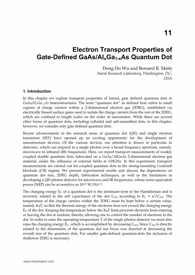
3.4 Double quantum dot photon-detector
Similar to Komiyama’s double quantum dot detector, our single photon detector consists of double quantum dots in a parallel geometry that is defined by metallic electrodes deposited on the 2DEG substrate surface. In this experiment we have used several different 2DEG substrates with the 2DEG depth ranging from 40 nm to 160 nm, and fabricated more than several hundred devices. Figure 14(a) shows the gate electrodes and the Ohmic contacts with the quantum dots located at the center of the white frame. Figure 14 (b) shows another SEM picture of the double quantum dots, which is a magnified view of the center part of Figure 14(a). The lower quantum dot (QD1) acts as a photon absorber and the upper quantum dot (QD2) functions as a single electron transistor.
(a) (b)
Fig. 14. (a) Overall SEM view of the NRL double quantum dot detector. (b) SEM picture of the electrode defined double quantum dots.
The gate electrodes were defined via e-beam lithography after which we deposited a 50 Å thick Cr layer (acts as a wetting layer) on the surface of a GaAs/AlGaAs heterostructure and then a 150 Å thick Au layer on top of the Cr layer. The diameters of QD1 and QD2, as defined by the surrounding electrodes, are roughly 250 nm with the diameter of the SET dot (QD2) slightly smaller than that of the absorber dot (QD1). As mentioned earlier, the actual size of the quantum dot is dependent upon the strength of the negative bias voltage applied to the gates: the stronger the bias voltage the smaller the quantum dot. As the capacitance and the electrochemical potential of the quantum dot are closely related to the number of isolated electrons, one can control the capacitance and the electrochemical potential by adjusting the gate voltage. The plunger gate G1 shown in Figure 14 provides experimental control of the SET dot's self capacitance (C1) and electrochemical potential (1), and the pair of gates labeled G2 control the absorber dot's self capacitance (C2) and electrochemical potential (2). The electrodes labeled G12 control the potential barrier that couples the SET dot and the absorber dot.
As the absorber (QD1) and the SET (QD2) are weakly coupled by the voltage on gates G12, the excited energy level of the absorber alters the energy levels of the SET. If an energy level
www.intechopen.com

Electron Transport Properties of Gate-Defined GaAs/AlxGa1-xAs Quantum Dot 263
of the SET aligns within the energy levels of the source and the drain, electrons begin to flow through the SET. These excited energy levels of the absorber and the SET are in what are referred to as meta-stable states, which survive typically on the order of or less than a few milli-seconds. This short meta-stable state is due to the fact that a finite probability exists that an electron from one of the large 2DEG reservoirs “hops” onto the absorber dot. This results in a change in the energy of the absorber dot, which can affect the energy level matching between the SET dot and source and drain, since the two dots are electrostatically coupled. Since the electron mobility is very high (3.0×105 cm2/Vs) and the electron density is very large (5.0x1011 cm-2) in the 2DEG, a significantly large number (~106 - 107) of electrons can flow through the SET within the short time of a meta-stable state, resulting in electric currents on the order of a pico-ampere. By employing a lock-in technique one can readily measure such currents. This operating principle is somewhat analogous to the photomultiplier tube as a single photon triggers a measureable electron flow in the detector.
Fig. 15. A schematic diagram of our experimental setup to measure low current signals from a device. This diagram shows the wiring between the electronic equipment and the gate and Ohmic pads on a device. A lock-in sources an AC signal (~ 0.1 V) and a simple voltage divider circuit 105:1 is connected to an Ohmic contact on the high side and is used to supply the V drop across the device. An Agilent E5270B Mainframe supplies the gate voltages through a homemade breakout box. Final data values can be read off of the Keithley digital multi-meters (DMM) and oscilloscope. The computer that collects data is housed in a separate room and is connected to the equipment via an optical fiber.
Ω50 Ω
Ω Ω
Ω
ΩΩ
Ω
Ω
www.intechopen.com

Fingerprints in the Optical and Transport Properties of Quantum Dots 264
The electrons (~106 -107) flowing through the SET result in an electric current, which is on the order of a pico-Ampere (10-12) or less. [1, 3, 12-14] In order to measure this weak current one should carefully design the experimental set up. Since electrical noises can induce currents much larger than pico-Ampere, it is necessary to minimize ambient electrical noises, which usually can be achieved by carrying out the measurements within a shielded room, and also by employing a lock-in technique. [15-17] An example is shown in Figure 15. A measurement includes the application of a source-drain voltage (or current source) over the device, or part of the device, and measuring the resulting current or voltage signal as a function of various parameters, such as the negative voltages applied to the depletion gates, temperature, electromagnetic fields, etc.
During the measurements it is important to keep the current and voltage across a device small enough in order to maintain the device temperature sufficiently cold. The energy associated with the voltage drop across the source and the drain, Vsd, should not exceed the electron thermal energy, KBTe, within the 2DEG. If eVsd > KBTe, then the electrons within the Fermi reservoirs may enter or leave the quantum dots at random and/or the higher energy charge states may become allowed within the dots. Then the electron flow through the quantum dot cannot be controlled. Therefore, it is necessary to limit the voltage drop across a device such that eVsd < KBT, where KB is the Boltzmann’s constant. For example, Vsd should be less than 345 V for Te = 4 K, or 8.62 V for Te = 100 mK.
3.5 Photon detection
A schematic diagram of our photon detection setup is shown in Figure 16. For this demonstration we used a double quantum-dot detector fabricated on 100 nm 2DEG, and employed an HP 85105 millimeter-wave controller and an HP W85104A test-set module, which were attached to an HP8510C Vector Network Analyzer. The millimeter-wave signal was sent through micro-coaxial cable (Lakeshore Type C cable). To modulate the signal we split the micro-coaxial cable and made two sets of dipole antennae, which face each other across an optical beam chopper (Stanford Research SR540) set to produce 1 - 2 Hz modulation. However, at the low modulation frequency, the chopper's blade did not rotate smoothly resulting in irregular modulation so much that the modulation interval was highly irregular. Also, we note that the millimeter-wave signal was highly attenuated through the micro-coaxial cables, as well as through the dipole-antenna to dipole-antenna coupling. We estimate the attenuation rate was much more than 5dB per foot for the micro-coaxial cable and the coupling efficiency through the dipole-antenna coupling to be less than 10%. Since the initial mm-wave input from the W85104A was approximately 50 W, and the transmission efficiency of the millimeter-wave photon through the coaxial cable and the dipole-antenna coupling was extremely poor, we think that the millimeter-wave signal radiated onto the double dot detector was sub-microwatts.
We measured the temperature dependent conductance as well as the bias voltage dependent conductance of our double dot device. The experiments indicate that although the millimeter-wave signal power was very weak our double dot device could detect the signal (Figure 17). However, the results may not indicate single photon detection. We think that our double dot detector could detect a few millimeter-wave photons at 100 mK.[18]
www.intechopen.com

Electron Transport Properties of Gate-Defined GaAs/AlxGa1-xAs Quantum Dot 265
Fig. 16. Experimental set up for the millimeter-wave photon detection with our double dot detector.
Fig. 17. The conductance variation as the double dot device detects millimeter-wave photons
While experiments indicate that it was possible to detect some photons at 110 GHz with the double quantum-dot structure shown in Figure 14, the detection efficient was very poor. We suspect that the inefficiency was largely due to the gate G2, which was supposed to function as an antenna. With its improper shape as an antenna, it did not efficiently pick up photons. Later we modified the double quantum dot detector, implementing bow-tie antenna geometry for the gate G2, as shown in Figure 18.
Also we attempted to reduce the quantum dot size in order to detect photons at an elevated temperature. As discussed earlier, a quantum dot detector should be operated at a temperature T that has a thermal energy KBT below the charging energy of the quantum dot. The charging energy EC is given as EC = e2/Cdot where Cdot is the self capacitance of the
www.intechopen.com

Fingerprints in the Optical and Transport Properties of Quantum Dots 266
quantum dot, which is proportional to the size of quantum dot. Hence, by reducing the quantum dot size, one can raise the charging energy EC, as well as the operating temperature T of the quantum dot detector.
Fig. 18. SEM images of a modified double quantum-dot detector. (a) Overall view. (b) Magnified view of the center of picture (a), showing double quantum dots and a bow-tie antenna. The lower quantum dot is coupled to a dipole (bow-tie) antenna fabricated to absorb THz frequencies, while the upper dot acts as a single electron transistor.
As a rule of thumb the depletion length that is the lateral depletion of the electrons around the gates is roughly equal to the depth of the 2DEG. This means that, for a smaller quantum dot, we need to use a shallower 2DEG substrate. For our experimental demonstration of a photon detector at temperatures considerably higher than 100 mK, we have fabricated about a hundred double quantum-dot detectors on 2DEG substrates with thickness ranging from 40 nm to 160 nm.
4. Leakage currents in GaAs/AlGaAs heterostructures
Our experiments revealed that the quantum dot detectors fabricated on a shallow 2DEG suffered from problems associated with overwhelming leakage currents. Within a GaAs/AlGaAs heterostructure the leakage currents increased dramatically as the 2DEG depth became shallower. Since the leakage currents dominate, it was not possible to obtain any discernible signal from the quantum dot detector. Also the leakage currents caused severe damage to the quantum dot gates, often resulting in a short circuit on the gates.
Measurements were performed to determine the currents that flow between the 2DEG and a laterally defined depletion gate on the wafer’s surface. Current is measured as a function of the voltage applied to the gate when the gate is biased with respect to the 2DEG underneath. While we expect that the current should be zero ideally or much less than pico-Amperes, the actual leakage current measured is orders of magnitude larger than anticipated. Even our numerical calculation, which was performed along with our experimental efforts, indicates that the leakage current is substantially larger than previously expected for shallow 2DEG wafers. Unless we find a way to prevent this large leakage it may lead to a limit for the maximum operating temperature obtainable for our quantum-dot photon detector.
(a) (b)
www.intechopen.com

Electron Transport Properties of Gate-Defined GaAs/AlxGa1-xAs Quantum Dot 267
Figure 19 shows a simple setup used to test the leakage currents within our GaAs/AlGaAs 2DEG substrate. The leakage current measurements were performed for several different 2DEGs with depths of 40 nm, 43 nm, 90 nm, and 160 nm. As shown in Figure 19, the voltage potential is applied directly to a gate and to an Ohmic contact in the reservoir. Any leakage current between the gate and the 2DEG is measured by a current amplifier (DL1211). The DL1211 converts the measured current signal into a voltage signal, which is read by the Keithley multimeter.
Fig. 19. A schematic experimental setup for the measurement of leakage currents in our 2DEG wafers. The voltage potential is supplied by an Agilent E5270B Precision Measurement Mainframe.
The leakage currents increased 6 orders of magnitude when the 2DEG depth was varied from 160 nm to 40 nm. Some of the shallowest (40 nm) 2DEG substrates generated leakage currents as high as tens of micro-Amperes, while the leakage current from the thickest one was much smaller, less than a pico-Ampere. When leakage currents are as high as several micro-Amperes the electron flow in and around the quantum dots cannot be controlled, and it is impossible to obtain any meaningful signal from the quantum dot detector. Our experiments further revealed that the strength of leakage currents vary depending on the individual 2DEG substrate. In other words, when we measure the leakage currents from two different 40 nm thick 2DEG substrates, we obtain very inconsistent results. This suggests us that the leakage current problem may not be entirely due to the intrinsic property of a shallow 2DEG, rather it may suggest that the problem is related to the defects in the 2DEG substrate.
Figure 20 shows an example of our leakage current data obtained from a 43 nm deep 2DEG at 4.2 K. The leakage currents increased linearly with the gate potential, and could reach as high as several hundred nano-Amperes. In order to investigate the origin of this leakage
www.intechopen.com

Fingerprints in the Optical and Transport Properties of Quantum Dots 268
current we performed numerical simulations, in which we assumed the leakage currents were through a 1-dimensional barrier. In this simplified model only the tunneling across a Schottky barrier from a metal to a GaAs layer under a reverse gate bias was considered. The model is so simplified that we did not include the charge carrier interaction with the heterostructure, such as how the charge carriers, after having passed the Schottky barrier, travel through several regions of GaAs and AlGaAs, including a heavily doped AlGaAs layer, before reaching the 2DEG. The inclusion of these would make the simulations more realistic. However it will require implementing a lot more difficult calculations in the simulations. So we only considered the problem only the top layer of GaAs. We know that this simulation is not realistic, but we think that it will give us some insights about the leakage currents.
Fig. 20. Leakage current data taken from a 43 nm deep 2DEG at 4.2 K. Leakage currents for this shallow 2DEG structure can be as high as hundreds of nano-Amperes.
The simulations indicate that a shallower 2DEG leads to a larger leakage current, and the leakage current can exceed a thousand nano-Amperes. These results are at least qualitatively consistent with our experimental results. A simulated result that shows the leakage current as a function of gate voltage is presented in Figure 21. Apparently the exponential relationship between the leakage current and the bias voltage is not consistent with our experiments. (See Figure 20) The discrepancy may be due to the fact that our model is too simple and does not reflect realistic conditions, for instance the scattering that the charge carriers experience, due to the Si dopants, as they pass from the lateral surface gates to the 2DEG, and the effect of lattice mismatching between GaAs and AlGaAs.
www.intechopen.com

Electron Transport Properties of Gate-Defined GaAs/AlxGa1-xAs Quantum Dot 269
In order to construct a device using quantum dots, one should minimize the leakage current since it not only prevents the proper control of the quantum dot but also sometimes leads to physical damage to the quantum dot. The gates surrounding the quantum dot are very small, typically less than 20 nm thick and a few tens of nm wide. Around the quantum point contacts formed by the gates the cross-sections of these metal-structures can be as small as a few tens of nm2. When the leakage current exceeds several hundred nano-Amperes, the current density near the quantum point contacts can exceed 1010 - 1011 A/m2. The current density may become high enough to fuse metallic structures near the quantum point contacts. This is what presumably happened to some of our quantum dot devices. An example is shown in Figure 22.
Fig. 21. An example of a numerical calculation showing the leakage current across a Schottky barrier from a metal to a GaAs layer under a reverse bias.
Our attempt to raise the operating temperature of a quantum dot photon detector did not succeed. The leakage current in shallower 2DEG materials remains one of the most significant technical challenges in achieving higher operating temperatures for single photon detectors. The origin of leakage currents in 2DEG substrates and a method to avoid them are topics for future research.
www.intechopen.com

Fingerprints in the Optical and Transport Properties of Quantum Dots 270
Fig. 22. SEM images of (a) BEFORE and (b) AFTER testing the quantum dots, which involves a large leakage current flowing through the device. The damage to the thin nanostructure gates near the center of the picture in (b) is due to the large leakage current that passes through the very small nanostructure (e.g. quantum point contacts between the gates).
5. References
[1] W. G. van der Wiel, S. DeFranceschi, J. M. Elzerman, T. Fujisawa, S. Tarucha, L. P. Kouwenhoven, Electron transport through double quantum dots, Reviews of Modern Physics 75 (2003).
[2] T. J. Thornton, M. Pepper, H. Ahmed, D. Andrews, G. J. Davies, One-Dimensional conduction in the 2D electron gas of a GaAs/AlGaAs Heterojunction, Phys. Rev. Lett. 56, 11 (1986).
[3] NATO ASI Series, Quantum Transport in Semiconductor Submicron Structures, Series E: Appl. Sci. 326 (1996)
[4] Vurgaftman, J. R. Meyer, D. H. Wu, K. Bussmann, and B. T. Jonker, Spectral simulation of GaAs and InAs quantum-dot terahertz detectors designed for higher-temperature operation, Journal of Applied Physics 100, 064509 (2006).
[5] P. O’connor, A. Dori, M. Feuer, R. Vounckx, Gold-germanium-based ohmic contacts to the two-dimensional electron gas at selectively doped semiconductor heterointerfaces, IEEE Transactions on Electron Devices ED-34, 4 (1987).
[6] M. Furno, F. Bonani, G. Ghione, Transfer matrix method modeling of inhomogeneous Schottky barrier diodes on silicon carbide, Solid-State Electronics 51, 466-474 (2007).
[7] J. Crofton, P. A. Barnes, A comparison of one, two, and three band calculations of contact resistance for a GaAs ohmic contact using the WKB approximation and a numerical solution to the Schrodinger equation, J. Appl. Phys. 69, 11 (1991).
[8] D. A. Muller, T. Sorsch, S. Moccio, F. H. Baumann, K. Evans-Lutterdot, G. Timp, The electronic structure at the atomic scale of ultrathin gate oxides, Nature 399, 758 (1999)
[9] H. van Houten, C. W. J. Beenakker, B. J. van Wees, Quantum point contacts Nanostructured Systems, M. A. Reed, Ed. (Academic Press, San Diego, 1992) 35, pp. 9-112 (1992)
(a) (b)
www.intechopen.com

Electron Transport Properties of Gate-Defined GaAs/AlxGa1-xAs Quantum Dot 271
[10] O. Astafiev, S. Komiyama, T. Kutsuwa, V. Antonov, Y. Kawaguchi, K. Hirakawa, Single-photon detector in the microwave range, Applied Physics Letters 80, 22 (2002).
[11] S. Komiyama, O. Astafiev, V. Antonov, T. Kutsuwa, H. Hirai, A single-photon detector in the far-infrared range, Nature 403, 405 (2000).
[12] L. P. Kouwenhoven, C. M. Marcus, P. L. McEuen, S. Tarucha, R. M. Westervelt, N. S. Wingreen, Electron transport in quantum dots, Proceedings of the Advanced Study Institute on Mesoscopic Electron Transport (1997).
[13] C. Livermore, C. H. Crouch, R. M. Westervelt, K. L. Campman, A. C. Gossard, The Coulomb Blockade in Coupled Quantum Dots, Science 274, 1332 (1996)
[14] L. P. Kouwenhoven, C. M. Marcus, P. L. McEuen, S. Tarucha, R. M. Westervelt, N. S. Wingreen, Electron transport in quantum dots, Mesoscopic Electron Transport, Kluwer Academic, Dordrecht (1997)
[15] F. Pobell, Matter and Methods at Low Temperatures, 2nd Edition (2009) [16] H. W. Ott, Noise Reduction Techniques in Electronic Systems, 2nd Edition (1988) [17] R. C. Richardson, E. N. Smith, Experimental Techniques in Condensed Matter Physics
at Low Temperatures, Advanced Book Classics (1998) [18] D. H. Wu, B. R. Matis, K. Bussmann, Scalable single photon detector for terahertz and
infrared applications, International Journal of High Speed Electronics and Systems 18, 4 (2008)
[19] B. J. van Wees, H. van Houten, C. W. J. Beenakker, J. G. Williamson, L. P. Kouwenhoven, D. van der Marel, C. T. Foxon, Quantized conductance of point contacts in a two-dimensional electron gas, Phys. Rev. Lett. 60, 9 (1988).
[20] T. H. Oosterkamp, T. Fujisawa, W. G. van der Wiel, K. Ishibashi, R. V. Hijman, S. Tarucha, L. P. Kouwenhoven, Microwave spectroscopy of a quantum-dot molecule, Nature 395, 873 (1998).
[21] L. P. Kouwenhoven, S. Jauhar, J. Orenstein, P. L. McQueen, Y. Nagamune, J. Motohisa, H. Sakaki, Observation of photon-assisted tunneling through a quantum dot, Phys. Rev. Lett. 73, 25 (1994).
[22] K. Ikushima, Y. Yoshimura, T. Hasegawa, S. Komiyama, T. Ueda, K. Hirakawa, Photon-counting microscopy of terahertz radiation, App. Phys. Lett. 88, 152110 (2006).
[23] S. M. Cronenwett, S. M. Maurer, S. R. Patel, C. M. Marcus, C. I. Duruoz, J. S. Harris Jr., Mesoscopic Coulomb blockade in one-channel quantum dots, Phys. Rev. Lett. 81, 26 (1998).
[24] S. Gustavsson, M. Studer, R. Leturcq, T. Ihn, K. Ensslin, D. C. Driscoll, A. C. Gossard, Frequency-selective single-photon detection using a double quantum dot, Phys. Rev. Lett. 99, 206804 (2007).
[25] S. R. Patel, S. M. Cronenwett, D. R. Stewart, A. G. Huibers, C. M. Marcus, C. I. Duruoz, J. S. Harris Jr., K. Campman, A. C. Gossard, Statistics of Coulomb Blockade Peak Spacings, Phys. Rev. Lett. 80, 20 (1998)
[26] M. H. Devoret, R. J. Schoelkopf, Amplifying quantum signals with the single-electron transistor, Nature 406, 1039 (2000)
[27] H. L. Stormer, Rev. Mod. Phys. 71, 875 (1999) [28] M. Pioro-Ladriere, J. H. Davies, A. R. Long, A. S. Sachrajda, L. Gaudreau, P. Zawadzki,
J. Lapointe, J. Gupta, Z. Wasilewski, S. Studenikin, Origin of switching noise in GaAs/AlxGa1-xAs lateral gated devices, Phys. Rev. B 72, 115331 (2005)
www.intechopen.com

Fingerprints in the Optical and Transport Properties of Quantum Dots 272
[29] H. Hashiba, V. Antonov, L. Kulik, A. Tzalenchuk, P. Kleinschmid, S. Giblin, S. Komiyama, Isolated quantum dot in application to terahertz photon counting, Phys. Rev. B 73, 081310(R) (2006)
[30] S. Kim, M. S. Sherwin, J. D. Zimmerman, A. C. Gossard, P. Focardi, D. H. Wu, Room temperature terahertz detection based on electron plasma resonance in an antenna-coupled GaAs MESFET, Appl. Phys. Lett. 92, 253508 (2008)
www.intechopen.com

Fingerprints in the Optical and Transport Properties of QuantumDotsEdited by Dr. Ameenah Al-Ahmadi
ISBN 978-953-51-0648-7Hard cover, 468 pagesPublisher InTechPublished online 13, June, 2012Published in print edition June, 2012
InTech EuropeUniversity Campus STeP Ri Slavka Krautzeka 83/A 51000 Rijeka, Croatia Phone: +385 (51) 770 447 Fax: +385 (51) 686 166www.intechopen.com
InTech ChinaUnit 405, Office Block, Hotel Equatorial Shanghai No.65, Yan An Road (West), Shanghai, 200040, China
Phone: +86-21-62489820 Fax: +86-21-62489821
The book "Fingerprints in the optical and transport properties of quantum dots" provides novel and efficientmethods for the calculation and investigating of the optical and transport properties of quantum dot systems.This book is divided into two sections. In section 1 includes ten chapters where novel optical properties arediscussed. In section 2 involve eight chapters that investigate and model the most important effects oftransport and electronics properties of quantum dot systems This is a collaborative book sharing and providingfundamental research such as the one conducted in Physics, Chemistry, Material Science, with a base textthat could serve as a reference in research by presenting up-to-date research work on the field of quantum dotsystems.
How to referenceIn order to correctly reference this scholarly work, feel free to copy and paste the following:
Dong Ho Wu and Bernard R. Matis (2012). Electron Transport Properties of Gate-Defined GaAs/AlxGa1-xAsQuantum Dot, Fingerprints in the Optical and Transport Properties of Quantum Dots, Dr. Ameenah Al-Ahmadi(Ed.), ISBN: 978-953-51-0648-7, InTech, Available from: http://www.intechopen.com/books/fingerprints-in-the-optical-and-transport-properties-of-quantum-dots/electron-transport-properties-of-gate-defined-gaas-alxga1-xas-quantum-dot

© 2012 The Author(s). Licensee IntechOpen. This is an open access articledistributed under the terms of the Creative Commons Attribution 3.0License, which permits unrestricted use, distribution, and reproduction inany medium, provided the original work is properly cited.


![LIST OF PUBLICATIONSshodhganga.inflibnet.ac.in/bitstream/10603/11617/5... · LIST OF PUBLICATIONS Journals Included in the Thesis [1] Observation of electron confinement in InP/GaAs](https://img.dokumen.tips/doc/110x75/5ec805791d45222e6334df55/list-of-pu-list-of-publications-journals-included-in-the-thesis-1-observation.jpg)