Embed Size (px)
Citation preview

1
Electromagnetic NDE
Peter B. Nagy
Research Centre for NDE
Imperial College London
2011
Aims and Goals
Aims
1 The main aim of this course is to familiarize the students with Electromagnetic (EM) Nondestructive Evaluation (NDE) and to integrate the obtained specialized knowledge into their broader understanding of NDE principles.
2 To enable the students to judge the applicability, advantages, disadvantages, and technical limitations of EM techniques when faced with NDE challenges.
Objectives
At the end of the course, students should be able to understand the:1 fundamental physical principles of EM NDE methods2 operation of basic EM NDE techniques3 functions of simple EM NDE instruments4 main applications of EM NDE

2
Syllabus
1 Fundamentals of electromagnetism. Maxwell's equations. Electromagnetic wave propagation in dielectrics and conductors. Eddy current and skin effect.
2 Electric circuit theory. Impedance measurements, bridge techniques. Impedance diagrams. Test coil impedance functions. Field distributions.
3 Eddy current NDE techniques. Instrumentation. Applications; conductivity, permeability, and thickness measurement, flaw detection.
4 Magnetic measurements. Materials characterization, permeability, remanence, coercivity, Barkhausen noise. Flaw detection, flux leakage testing.
5 Alternating current field measurement. Alternating and direct current potential drop techniques.
6 Microwave techniques. Dielectric measurements. Thermoelectric measurements.
7 Electromagnetic generation and detection of ultrasonic waves, electromagnetic acoustic transducers (EMATs).

3
1 Electromagnetism
1.1 Fundamentals
1.2 Electric Circuits
1.3 Maxwell's Equations
1.4 Electromagnetic Wave Propagation
1.1 Fundamentals of Electromagnetism

4
Electrostatic Force, Coulomb's Law
x
z
y
r
Q2
Q1
Fe
Fe
Fe Coulomb force
Q1, Q2 electric charges (± ne, e ≈ 1.602 × 10⁻¹⁹ As)
er unit vector directed from the source to the target
r distance between the charges
ε permittivity (ε0 ≈ 8.85 × 10⁻¹² As/Vm)
1 2e 24 x
Q dQ xdrr
=πε
F e
2 , 2dQ q dA dA d= = πρ ρ
1e 3
02xQ q x d
r
∞
ρ=
ρ ρ= ∫
εeF
2 22 2
, d r rr xdr r x
ρρ = − = =
ρ−
1e 22
x
r x
Q q x drr
∞
== ∫
εeF
1e 2
xQ q=
εeF
x
dQ2
Q1
Fe
ρ
dρ
r
infinite wall of uniform charge
density q
independent of x
1 2e 24 r
Q Qr
=πε
F e
Electric Field, Plane Electrodes
Qt
Fe
x
z
y
e 2t xQ q
=εeF
infinite wall of uniform charge density q
2 xq
=ε
E e
E+Q -Q
A
QqA
=
charged parallel plane electrodes Q
xq
≈ε
E e
e tQ=F E

5
e tQ=F E
Electric Field, Point Sources
e 24s t
rQ Q
r=
πεF e
24s
rQ
r=
πεE e
monopole
+Qs
+Qs
-Qs
1 32sQ dE
r≈
πε
2 34sQ dE
r≈
πε
+Qs
-Qs
d
E1
E2
E1
dipole
Electric Field of Dipole
z z R RE E= +E e e
3/ 2 3/ 22 2 2 2
/ 2 / 24 ( / 2) ( / 2)
sz
Q z d z dEz d R z d R
⎡ ⎤− +⎢ ⎥= −⎢ ⎥πε ⎡ ⎤ ⎡ ⎤− + − +⎢ ⎥⎣ ⎦ ⎣ ⎦⎣ ⎦
( )23 3cos 1
4s
zQ dE
r≈ θ −
πε
3/ 2 3/ 22 2 2 24 ( / 2) ( / 2)s
RQ R RE
z d R z d R
⎡ ⎤⎢ ⎥= −⎢ ⎥πε ⎡ ⎤ ⎡ ⎤− + − +⎢ ⎥⎣ ⎦ ⎣ ⎦⎣ ⎦
33 sin 28
sR
Q dEr
≈ θπε
2 2 2r z R= + cosz r= θ sinR r= θ
R
z
+Qs
-Qs
d
θ
rr+
r
PEz
ER
E

6
Electric Dipole in an Electric Field
+Q
-Q
pe
Fe
E EE=E e
e dQ Q d= =p d e
e e Q= × = ×T d F d E
e Q=F E
pe electric dipole moment
Q electric charge
d distance vector
E electric field
Fe Coulomb force
Te twisting moment or torque
Fe e e= ×T p E
Electric Flux and Gauss’ Law
q charge (volume) density
D electric flux density (displacement)
E electric field (strength, intensity)
ε permittivity
ψ electric flux
Qenc enclosed charge
closed surface S
D
dS
Qenc
Sdψ = ∫∫ D Si
= εD E
d dψ = D Si
Sd dS=S e
encV
q dV Qψ = =∫∫∫
q∇ =Di

7
Electric Potential
W work done by moving the charge
Fe Coulomb force
ℓ path length
E electric field
Q charge
U electric potential energy of the charge
V potential of the electric field
E
QFe
dℓ
A
BB A ABU U U WΔ = − =
edW = − F i dℓ
BAB
AW Q= − ∫ Eidℓ
U V Q=
BB A
AV V VΔ = − = − ∫ Eidℓ
Capacitance
+Q
-Q
E
C capacitance
V voltage difference
Q stored charge
Q CV=
+
-
S+ -
SV V V= − = − ∫ Eidℓ
QCV
=
E
+Q
-Q
A
-Q
E
+Q
dℓ
QDA
ACDE
V E
⎫≈ ⎪⎪ ε⎪ ≈⎬= ⎪ε⎪⎪≈ ⎭

8
Current, Current Density, and Conductivity
I currentQ transferred charget timeJ current densityA cross section arean number density of free electronsvd mean drift velocitye charge of protonm mass of electronτ collision timeΛ free pathv thermal velocityk Boltzmann’s constantT absolute temperatureσ conductivity
dQIdt
=
dI d= J Ai
I d= ∫∫ J Ai
dne= −J v
ddQ ne d dt= − v Ai
dm e= −τv E
vΛ
τ =
21 32 2
mv kT=
E
dA
2nem
τ= = σJ E E
Resistivity, Resistance, and Ohm’s Law
V voltage
I current
R resistance
P power
σ conductivity
ρ resistivity
L length
A cross section area
I
+_V
A
dℓ
0 0
L Ld dRA A
ρ= =∫ ∫
σ
i i
i
LRA
ρ= ∑
1ρ =
σ
LRA
ρ=
+
-
S+ -
SV V V= − = − ∫ Eidℓ
0 0
L LJ dV d I I RA
= = =∫ ∫σ σ
VRI
=
dU dQP V V Idt dt
= = =

9
Magnetic Field
BQ
Fm
dv
e Q=F E
m Q= ×F v B
( )Q= + ×F E v B
F Lorenz forcev velocityB magnetic flux densityQ charge
+I -I
B
pm magnetic dipole moment(no magnetic monopole)
N number of turnsI currentA encircled vector area
m N I=p A
pm
Magnetic Dipole in a Magnetic Field
m Q= ×F v B
pm magnetic dipole moment
Q charge
v velocity
R radius vector
B magnetic flux density
Fm magnetic force
Tm twisting moment or torque
m N I=p A
+I
-Ipm
Fm
B
Fm
2m 2 r v
Qv RR
= π ×π
p e e
2A R= πQN I =τ
2 Rvπ
τ =
m12
Q= ×p R v
m m12
= ×T R F
22
m m m0
1 1cos2 2
T R F d R Fπ
= α α =∫π
m m= ×T p B

10
Magnetic Field Due to Currents
2 34 4s s
rQ Q
r r= = =
πε πεE e rCoulomb Law:
= εD E
= μB H
Biot-Savart Law: 2 34 4rI d Id
r r= × = ×
π πH e e rdℓ
dℓ
I
dℓ r
HH magnetic field
μ magnetic permeability
24 rI d
r= ×∫
πH e e
Ampère’s Law
24 rI dd
r= ×
πH e e
encS
d Q=∫∫ D SiGauss’ Law:
infinite straight wire
2 2 2 3/ 244 ( )I d R I R dd
rr Rθ θ= =ππ +
H e e
2 2 3/ 202 2( )
I R d IHRR
∞θ = =∫
π π+
2H ds H R Iθθ = π =∫
dℓ
I
dℓ
R
Hrℓ
s
2IH
Rθ =π
Biot-Savart Law:
Ampère’s Law:
Ampère’s Law: encd I=∫ H si
∇× =H J

11
N IΦ = μ Λ
Є dV NdtΦ
= − =
Induction, Faraday’s Law, Inductance
E induced electric field
B magnetic flux density
t time
Є induced electromotive force
s boundary element of the loop
Φ magnetic flux
S surface area of the loop
I N
Φ
V
μ magnetic permeability
N number of turns
I current
Λ geometrical constant
L (self-) inductanceI LN
Φ =
2L N= μ Λ
SdΦ = ∫∫B Si
Є ddtΦ
= −
t∂
∇× = −∂BE
dIV Ldt
=
B
Є d= ∫ E si
ЄS
dt
∂= − ∫∫
∂B Si
Electric Boundary ConditionsFaraday's law:
t∂
∇× = −∂BE
Gauss' law:
q∇ =Di
xt
medium I
medium II
DIθΙ
boundary
DII
DII,t
DII,n
θΙΙ
DI,n
DI,t
xn
xt
medium I
medium II
EI
θΙ
EIIEI,t EII,n
θΙΙ
EI,n
EII,t
xn
I,n II,nD D=
I I,n II II,nE Eε = ε
I,t II,tE E=
I I,n II II,ntan tanE Eθ = θ
I III II
tan tanθ θ=
ε ε
tangential component of the electric field E is continuousnormal component of the electric flux density D is continuous

12
Magnetic Boundary ConditionsAmpère's law:
t∂
∇× = +∂DH J
Gauss' law:
0∇ =Bi
xt
medium I
medium II
BIθΙ
boundary
BII
BII,t
BII,n
θΙΙ
BI,n
BI,t
xn
xt
medium I
medium II
HI
θΙ
HII
HII,t
HII,n
θΙΙ
HI,n
HI,t
xn
I,n II,nB B=
I I,n II II,nH Hμ = μ
I,t II,tH H=
I I,n II II,ntan tanH Hθ = θI II
I II
tan tanθ θ=
μ μ
tangential component of the magnetic field H is continuousnormal component of the magnetic flux density B is continuous
1.2 Electric Circuits

13
Є
Electric Circuits, Kirchhoff’s Laws
Є electromotive forceVi potential drop on ith element
Kirchhoff’s junction rule (current law):
Kirchhoff’s loop rule (voltage law):
0iV =∑
0=∫ EidℓI
+_
1R 2R
4R
3R1V 2V
4V3V0V
0iI =∑
encS
Q d= ∫∫ D Si
Ii current flowing into a junction from the ith branch
+_Є
1I 2I
4I
1R 2R
4R
3R
Circuit Analysis
Loop Currents:
Kirchhoff’s Laws:
+_Є
1I 2I
4I
1R 2R
3R1V 2V
3V0V
+_Є
1I 2I
4I
1R 2R
4R
3R1i 2i
4R
4V1 2 41 2 4
0V V VR R R
− − =
1 4 0 0V V V+ − =
2 3 4 0V V V+ − =
322 3
0VVR R
− =
1 1 1 2 4 0( ) 0i R i i R V+ − − =
2 2 2 3 1 2 4( ) 0i R i R i i R+ − − =

14
DC Impedance Matching
2g
2g g, where
(1 )
V RPR R
ξ= ξ =
+ ξ
22 V
P I V I RR
= = =
g g
g gand
V V RI V
R R R R= =
+ +
2g
3g
1(1 )
VdPd R
− ξ=
ξ + ξ
2g
max gg
when4V
P R RR
= =
_ VgV
gR
R+
P IV=W QV=
AC ImpedanceI
V dIV Ldt
=
I
V 1V I dtC
= ∫
I
V V R I=
VZ i LI
= = ωVZ RI
= =1VZ
I i C= =
ω
0
0ZiVZ R i X Z e
Iϕ= = + =
0 2 20
VZ R XI
= = +
-1arg( ) - tanZ V IXZR
= ϕ = ϕ ϕ =
( )0 0( ) Ii t i tI t I e I eω + ϕ ω= =
( )0 0( ) Vi t i tV t V e V eω + ϕ ω= =
ReI I=
ReV V=
0 0 IiI I e ϕ=
0 0 ViV V e ϕ=

15
AC Power
ReI I=( )0 0( ) Ii t i tI t I e I eω + ϕ ω= =0( ) cos( )II t I t= ω + ϕ
ReV V=( )0 0( ) Vi t i tV t V e V eω + ϕ ω= =0( ) cos( )VV t V t= ω + ϕ
* *0 01 1( ) ( )2 2
P I t V t I V= =( ) ( )P I t V t= ReP P=
( )0 0
12
I ViP I V e ϕ − ϕ=0 01 cos( )2 I VP I V= ϕ − ϕ
real notation complex notation correspondence
cos( ) cos cos sin sinα + β = α β − α β
cos( ) cos cos sin sinα − β = α β + α β
1 1cos( ) cos( ) cos cos2 2
α + β + α − β = α β
cos sinie iα = α + α
reminder:
AC Impedance Matching
VgV
gZ
Z≈
ReP P=
2 *g*
*g g
1 Re Re2 2 ( )( )
V ZP I VZ Z Z Z
⎧ ⎫⎪ ⎪= = ⎨ ⎬+ +⎪ ⎪⎩ ⎭
( )*g g g,Z Z R R X X= = = −
2gmax
g8V
PR
=
2g
2Re2 4
g g
g
V R i XP
R
⎧ ⎫−⎪ ⎪= ⎨ ⎬⎪ ⎪⎩ ⎭

16
1.3 Maxwell's Equations
Vector Operations
( )0
limSS S→
⎧ ⎫∫∇× = ⎨ ⎬⎩ ⎭
AA e ii dℓCurl of a vector:
0lim yS x z
V
dAA A
V x y z→
⎧ ⎫∫∫ ∂∂ ∂⎪ ⎪∇ = = + +⎨ ⎬ ∂ ∂ ∂⎪ ⎪⎩ ⎭
A SA
iiDivergence of a vector:
x y zx y z∂φ ∂φ ∂φ
∇φ = + +∂ ∂ ∂
e e eGradient of a scalar:
2 2 22
2 2 2x y z∂ φ ∂ φ ∂ φ
∇ φ = + +∂ ∂ ∂
Laplacian of a scalar:
2 2 2 2x x y y z zA A A∇ = ∇ + ∇ + ∇A e e eLaplacian of a vector:
2( ) ( )∇× ∇× = ∇ ∇ ⋅ − ∇A A AVector identity:
x y zx y z∂ ∂ ∂
∇ = + +∂ ∂ ∂
e e eNabla operator:
2 2 22
2 2 2x y z∂ ∂ ∂
∇ = ∇ ∇ = + +∂ ∂ ∂
iLaplacian operator:
y yx xz zx y z
A AA AA Ay z z x x y
∂ ∂⎛ ⎞ ⎛ ⎞∂ ∂∂ ∂⎛ ⎞∇× = − + − + −⎜ ⎟ ⎜ ⎟⎜ ⎟∂ ∂ ∂ ∂ ∂ ∂⎝ ⎠⎝ ⎠ ⎝ ⎠A e e ea

17
Maxwell's Equations
Ampère's law:
Faraday's law:
Gauss' law:
Gauss' law:
t∂
∇× = +∂DH J
t∂
∇× = −∂BE
q∇ =Di
0∇ =Bi
Field Equations:
conductivity = σJ E
permittivity = εD E
permeability = μB H
Constitutive Equations:
(ε0 ≈ 8.85 × 10⁻¹² As/Vm)
(µ0 ≈ 4π × 10-7 Vs/Am)0 rμ = μ μ
0 rε = ε ε
1.4 Electromagnetic Wave Propagation

18
Electromagnetic Wave Equation
Maxwell's equations:
( )it
∂∇× = + = σ+ ωε
∂DH J E
it
∂∇× = − = − ωμ
∂BE H
0∇⋅ =E
0∇⋅ =H
( ) ( )i i∇× ∇× = − ωμ σ + ωεH H
( ) ( )i i∇× ∇× = − ωμ σ + ωεE E
2( ) ( )∇× ∇× = ∇ ∇ ⋅ − ∇A A A
2 ( )i i∇ = ωμ σ + ωεE E
2 ( )i i∇ = ωμ σ + ωεH H
2 ( )k i i= − ωμ σ + ωε
2 2( )k∇ + =E 0
2 2( )k∇ + =H 0
( )0
i t k xy y yE E e ω −= =E e e
( )0
i t k xz z zH H e ω −= =H e e
Example plane wave solution:
Wave equations:
Harmonic time-dependence: 0 0andi t i te eω ω= =E E H H
Wave Propagation versus Diffusion
Propagating wave in free space:
/ ( / )0
x i t xyE e e− δ ω − δ=E e
/ ( / )0
x i t xzH e e− δ − ω − δ=H e
Diffusive wave in conductors:
kcω
=
0 0
1c =μ ε
1 ik i= − ωμσ = −δ δ
1f
δ =π μσ
( / )0
i t x cyE e ω −=E e
( / )0
i t x czH e ω −=H e
2 ( )k i i= − ωμ σ + ωε
δ standard penetration depth
c wave speed
k wave number
Propagating wave in dielectrics:
d0 0 r
1c =μ ε ε r
d
cnc
= = ε
n refractive index
19
Intrinsic Wave Impedance( )
0i t k x
y y yE E e ω −= =E e e ( )0
i t k xz z zH H e ω −= =H e e
( )it
∂∇× = + = σ+ ωε
∂DH J E
( )0
z i t k xy y
H i k H ex
ω −∂∇ × = − =
∂H e e
( )k i i= − ωμ σ + ωε
Propagating wave in free space:0
00
377μη = ≈ Ω
ε
Propagating wave in dielectrics:0 0
0 r nμ η
η = ≈ε ε
Diffusive wave in conductors:1i iωμ +
η = =σ σδ
0
0
E iH i
ωμη = =
σ+ ωε
PolarizationPlane waves propagating in the x-direction:
( ) ( )0 0
i t k x i t k xy y z z y y z zE E E e E eω − ω −= + = +E e e e e
( ) ( )0 0
i t k x i t k xz z y y z z y yH H H e H eω − ω −= + = +H e e e e
0 00
0 0
y z
z y
E EH H
η = = −
0 0 0 0y zi iy y z zE E e E E eφ φ= =
y
z
y
z
y
z
Ey
EzE
0º (or 180º)y zφ − φ =
linear polarization elliptical polarization
90º (or 270º)y zφ − φ =
circular polarization
E E
20
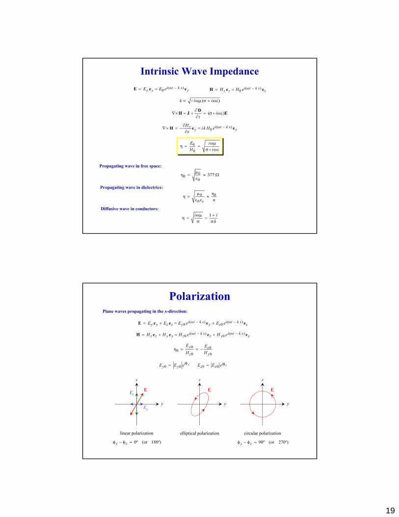
Reflection at Normal Incidence
x
y
incident
reflected transmitted
I( )i i0
i t k xyE e ω −=E e
Ii0 ( )i
Ii t k x
zE e ω −=η
H e
I( )r r0
i t k xyE e ω +=E e
Ir0 ( )r
Ii t k x
zE e ω += −η
H e
II( )t t0
i t k xyE e ω −=E e
IIt0 ( )t
IIi t k x
zE e ω −=η
H e
I medium II medium
Boundary conditions:
( 0 ) ( 0 )y yE x E x− += = = i0 r0 t0E E E+ =
( 0 ) ( 0 )z zH x H x− += = = i0 r0 t0H H H+ =
i0 r0 t0
I I II
E E E− =
η η η
r0 II Ii0 II I
ERE
η − η= =
η + η
t0 IIi0 II I
2ETE
η= =
η + η
Reflection from Conductors
x
y
incident
reflected transmitted“diffuse” wave
I dielectric II conductor
1 0f
δ = ≈π μσ
0II I
in
ηωμη = << η =
σ
II III I
1R η − η= ≈ −
η + η
• negligible penetration
• almost perfect reflection with phase reversal

21
Axial Skin Effect
-0.2
0
0.2
0.4
0.6
0.8
1
0 1 2 3Normalized Depth, x / δ
Nor
mal
ized
Dep
th P
rofil
e, F
magnitudereal part
0 ( ) i tyE F x e ω=E e
0 ( ) i t zH F x e ω=H e
δ standard penetration depth
/ /( ) x i xF x e e− δ − δ=
1f
δ =π μσ
x
y
propagating wave diffuse wave
dielectric (air) conductor
Transverse Skin Effect
0 0( )zE E J k r=
1f
δ =π μσ
2k i= − ωμσ1 ik = −δ δ
012 ( )
k IEa J k a
=πσ
Jn nth-order Bessel functionof the first kind
02 1
( )( )2 ( )z
k a J k rIJ rJ k aa
=π
z
r
current density
conductor rod
current, I 2a
0
1
2
3
4
5
6
7
8
0 0.2 0.4 0.6 0.8 1Normalized Radius, r/a
Nor
mal
ized
Cur
rent
Den
sity
, J/J
DC
a/δ = 1a/δ = 3a/δ = 10
magnitude, DC 2IJa
=π

22
Transverse Skin Effect
z
r
current density
conductor rod
current, I 2a
0.1
1
10
100
0.01 0.1 1 10 100
Normalized Radius, a/δ
Nor
mal
ized
Res
ista
nce,
R/R
0
R ∝ ω
0R R≈
VZ R i XI
= = +
0 2RA a
= ρ =σπ
0
1
( )( )2 ( )
JGJ
ξ ξξ =
ξ
0 ( )Z R G k a=
/lim (1 )
2a
aG iδ→∞
= +δ
/lim
2aR
aδ→∞=
σ π δ

23
2 Eddy Current Theory
2.1 Eddy Current Method
2.2 Impedance Measurements
2.3 Impedance Diagrams
2.4 Test Coil Impedance
2.5 Field Distributions
2.1 Eddy Current Method

24
Eddy Current Penetration Depth0 ( ) i t
yE F x e ω=E e
0 ( ) i t zH F x e ω=H e
δ standard penetration depth
/ /( ) x i xF x e e− δ − δ=
aluminum (σ = 26.7 × 10⁶ S/m or 46 %IACS)
-0.2
0
0.2
0.4
0.6
0.8
1
0 1 2 3Depth [mm]
Re
F
f = 0.05 MHzf = 0.2 MHzf = 1 MHz
f = 0.05 MHzf = 0.2 MHzf = 1 MHz
-0.2
0
0.2
0.4
0.6
0.8
1
0 1 2 3Depth [mm]
| F |
1f
δ =π μσ
Eddy Currents, Lenz’s Law
conducting specimen
eddy currents
probe coil
magnetic field
s p s( )dVdt
= − Φ − Φ
p p∇× =H J
s p s( )t
∂∇× = −μ −
∂E H H
s s= σJ E
p p pN IΦ = μ Λ
s sI V∝ σ
s s sIΦ = μ Λs s∇× =H J
secondary(eddy) current
(excitation) currentprimarymagnetic flux
primary
magnetic fluxsecondary
p p s( )dV Ndt
= − Φ − Φ
pprobe
p( , , , , ... )
VZ
I= ω σ μ

25
2.2 Impedance Measurements
Impedance Measurements
pI p
e
( )( )
( )V
K ZI
ωω = =
ωIe VpZp
Ve
Ze
VpZp
Voltage divider:
Current generator:
Iep p
Ve e p
( )( )
( )V Z
KV Z Z
ωω = =
ω +
Ve p
V
( )1 ( )
K Z ZK
ω=
− ω

26
Resonance
Ve
R
L VoC
0
0.2
0.4
0.6
0.8
1
0 1 2 3Normalized Frequency, ω/Ω
Tran
sfer
Fun
ctio
n, |
K|
Q = 2Q = 5Q = 10
p 2( )1
i LZLC
ωω =
− ω
po
e p
( )( )( )( ) ( )
ZVKV R Z
ωωω = =
ω + ω
2/( )
1 /i L RK
i L R LCω
ω =+ ω − ω
2 2( )
1 /
iQK i
Q
ωΩω =
ω+ − ω ΩΩ
1LC
Ω =
C RQ R R CL L
= = = ΩΩ
o 211
4Qω = Ω −
Wheatstone Bridge
32 2e 1 2 4 3
( )( )( )
ZV ZK GV Z Z Z Z
⎛ ⎞ωω = = −⎜ ⎟ω + +⎝ ⎠
VeV2
Z1 Z4
Z2 Z3
+_ G
322
1 40 if ZZV
Z Z= =
1 4 0Z Z R= =
*2 cZ i L R= ω +
3 c cZ i L R= ω +
R0 reference resistanceLc reference (dummy) coil inductanceRc reference coil resistanceL* complex probe coil inductance
2 3 (1 )Z Z= + ξ
probe coil reference coil
3 3
0 3 0 3
(1 )( )(1 )
Z ZK GR Z R Z
⎛ ⎞+ ξω = −⎜ ⎟+ + ξ +⎝ ⎠
0( ) ( )K G Kω ≈ ω ξ
3 00 2
0 3( )
( )Z RK
R Zω =
+

27
Impedance Bandwidth
3 c cZ i L R= ω +
R0 = 100 Ω, Rc = 10 Ω
0( ) ( )K G Kω ≈ ω ξ
3 00 2
0 3( )
( )Z RK
R Zω =
+
0 1 2 30
0.1
0.2
0.3
0.4
0.5
Frequency [MHz]
Tran
sfer
Fun
ctio
n, |
K0
|
Lc = 100 µHLc = 20 µHLc = 10 µH
c 00 2
c 0
/( )1 ( / )
L RKL R
ωω ≈
+ ω
3 cZ i L≈ ω
0p
c
RL
ω =
0 p1( )2
K ω ≈
02
c
2 RL
ω =
0 1,22( )5
K ω ≈
01
c2RL
ω =
21
4ω=
ω
2 1c 2 1
62 or 120%5r
BB ω − ω= = =
ω ω + ω
( , , , ,...)ξ = ξ ω σ μ
2.3 Impedance Diagrams

28
Examples of Impedance Diagrams
Im(Z)
Re(Z)
L
C
Im(Z)
Re(Z)0
Ω-
Ω+
∞
L
C
R 0
Ω-
Ω+
∞R
Im(Z)
Re(Z)
R
L
C
0 Ω∞ R
Im(Z)
Re(Z)
R2
L
C
0 Ω∞ R1 R1+R2
R1
Magnetic Coupling
12 2122 11
Φ Φ= = κ
Φ Φ
2 2 21 22( )dV Ndt
= Φ + Φ
1 1 11 12( )dV Ndt
= Φ + Φ
1 11 12 1
2 21 22 2
V L L Ii
V L L I⎡ ⎤ ⎡ ⎤ ⎡ ⎤
= ω⎢ ⎥ ⎢ ⎥ ⎢ ⎥⎣ ⎦ ⎣ ⎦ ⎣ ⎦
12 21 11 22L L L L= = κ
221 11
1
NL LN
= κ 112 22
2
NL LN
= κ
1 1121 11
1
I LN
Φ = κΦ = κ 2 2212 22
2
I LN
Φ = κΦ = κ
1 1111
1
I LN
Φ = 2 2222
2
I LN
Φ =
I1
N1 N2 V2
Φ11
V1
I2
Φ22Φ12 Φ21,
V1 V2L , L , L11 12 22
I1 I2

29
Probe Coil Impedance
e 22222n
e 22 e 22
R i LLZ iR i L R i L
− ωω= + κ
+ ω − ω
2 222 e 222 2n 2 2 2 2 2 2e e22 22
(1 )LL RZ i
R L R Lωω
= κ + − κ+ ω + ω
V2V1
I1 I2
L , L , L11 12 22 Re
2 2 e 12 1 22 2V I R i L I i L I= − = ω + ω
122 1
e 22
i LI IR i L
− ω=
+ ω
1 11 1 12 2V i L I i L I= ω + ω
2 212
1 11 1e 22
( )L
V i L IR i L
ω= ω +
+ ω
2 212
coil 11e 22
LZ i L
R i Lω
= ω ++ ω
222n22e
LZ iR i L
ω= + κ
+ ω
1 11 12 1
2 12 22 2
V L L Ii
V L L I⎡ ⎤ ⎡ ⎤ ⎡ ⎤
= ω⎢ ⎥ ⎢ ⎥ ⎢ ⎥⎣ ⎦ ⎣ ⎦ ⎣ ⎦
1coil
1
VZI
=
coiln
11(1 )ZZ i
L= = + ξ
ω
coil ref [1 ( , , )]Z Z= + ξ ω σ
ref 11Z i L≈ ω
2 211 2212L L L= κ
( )κ = κ
Impedance Diagram22 eL Rζ = ω /
2n n 2Re
1R Z ζ
= = κ+ ζ
22
n n 2Im 11
X Z ζ= = − κ
+ ζ
n n0 0
lim 0 and lim 1R Xω→ ω→
= =
2n nlim 0 and lim 1R Xω→∞ ω→∞
= = − κ
2 2n n( 1) and ( 1) 1
2 2R Xκ κ
ζ = = ζ = = −
0
0.1
0.2
0.3
0.4
0.5
0.6
0.7
0.8
0.9
1
0 0.1 0.2 0.3 0.4 0.5Normalized Resistance
Nor
mal
ized
Rea
ctan
ce
κ = 0.6κ = 0.8κ = 0.9
Re=10 Ω
Re=5 Ω
Re=30 Ω
22 e e3 H, = 1 MHz, / 10%L f R R= μ Δ = lift-off trajectories are straight:
n n1X R= − ζ
conductivity trajectories are semi-circles
2 22 22n n 1
2 2R X
⎛ ⎞ ⎛ ⎞κ κ+ − + =⎜ ⎟ ⎜ ⎟
⎝ ⎠ ⎝ ⎠

30
Electric Noise versus Lift-off Variation
0.32
0.34
0.36
0.38
0.40
0.42
0.28 0.3 0.32 0.34 0.36 0.38“Horizontal” Impedance Component
“Ver
tical
”Im
peda
nce
Com
pone
nt
0.32
0.34
0.36
0.38
0.40
0.42
0.28 0.3 0.32 0.34 0.36 0.38Normalized Resistance
Nor
mal
ized
Rea
ctan
ce lift-offlift-off
“physical” coordinates rotated coordinates
nZ ⊥ΔnZΔ
Conductivity Sensitivity, Gauge Factor
22 e e3 H, = 1 MHz, 10 , 1L f R R= μ = Ω Δ = ± Ω
nnorm
e e/Z
FR R
⊥Δ=
Δn
abse e/Z
FR RΔ
=Δ
0 (1 )R R F= + ε //
R RF Δ=
Δ
0
0.02
0.04
0.06
0.08
0.10
0.12
0.14
0 0.2 0.4 0.6 0.8 1Frequency [MHz]
Gau
ge F
acto
r, F
absolute
normal0.32
0.34
0.36
0.38
0.40
0.42
0.28 0.3 0.32 0.34 0.36 0.38Normalized Resistance
Nor
mal
ized
Rea
ctan
ce lift-off
nZ ⊥Δ
nZΔ

31
Conductivity and Lift-off Trajectories
lift-off trajectories are not straightconductivity trajectories are not semi-circles
0
0.1
0.2
0.3
0.4
0.5
0.6
0.7
0.8
0.9
1
0 0.1 0.2 0.3 0.4 0.5Normalized Resistance
Nor
mal
ized
Rea
ctan
ce
κ
lift-off
conductivity
eLRA
≈σ
( )κ ≈ κ
e ( )LR
A≈
σ σ( , )κ ≈ κ σ finite probe size
0
0.1
0.2
0.3
0.4
0.5
0.6
0.7
0.8
0.9
1
0 0.1 0.2 0.3 0.4 0.5Normalized Resistance
Nor
mal
ized
Rea
ctan
ce
κlift-off
conductivity
2.4 Test Coil Impedance

32
Air-core Probe Coils
single turn L = a L = 3 a
center 2IHa
=
24 rI dd
r= ×
πH e e
a coil radiusL coil length
encd I=∫ H si
center/lim
L a
N IHL→∞
=
2axis 2 2 3/ 22( )
I aHa z
=+
Infinitely Long Solenoid Coil
encd I=∫ H si
sJ n I=
1 2( ) ( ) 0z zL H r L H r− =
for outside loops (r1,2 > a)
0zH =
1 2( ) ( ) 0z zL H r L H r− =
for inside loops (r1,2 < a)
constantzH =
1 2 s( ) ( )z zL H r L H r L J− =
1 s( )zIH r J n I NL
= = =
for encircling loops (r1 < a < r2)
inside loop outside loopencircling
2a
L
+ Js_ Js
z

33
Magnetic Field of an Infinite Solenoid with Conducting Core
in the air gap (b < r < a) Hz = Js
in the core (0 < r < b) Hz = H1 J0(kr)
Jn nth-order Bessel function of the first kind
s1
0( )J
HJ k b
=
+ Js_ Js
2 a2 b
z
0s
0
( )( )z
J k rH J
J k b=
2 2( )k∇ + =H 0 2k i= − ωμσ1 ik = −δ δ
22
21 0zk Hr rr
⎛ ⎞∂ ∂+ + =⎜ ⎟∂∂⎝ ⎠
2 2s
02 ( ) ( )
bzH r r dr a b JΦ = πμ + πμ −∫
z zB dA H dAΦ = = μ∫∫ ∫∫
Magnetic Flux of an Infinite Solenoid with Conducting Core
+ Js_ Js
2 a2 b
z0
s0
( )( )
( )zJ k r
H r JJ k b
=
( )z zH H r=
szH J=
0zH =
2 2s 0
0 0
2[ ( ) ]( )
bJ J k r r dr a b
J k bΦ = πμ + −∫
0 1( ) ( )J d Jξ ξ ξ = ξ ξ∫
1 2 2s
0
2 ( )[ ]
( )b J k b
J a bk J k b
Φ = πμ + −
1
0
2 ( )( )
( )J
gJ
ξξ =
ξ ξ
2 2s [1 ( )]J a b g k bΦ = πμ − −

34
For an empty solenoid (b = 0):
Normalized impedance:
1 1 1, ,s LJ n I V i V NV n LV= = ωΦ = =
1 2 2 2 2s
[1 ( )]LV VZ n L i a b g k b n L
I J= = = ωπμ − −
2 2e eZ i a n L i X= ωπμ =
22
2 is called fill-factor ( lift-off)ba
κ = ≈
2n
e1 [1 ( )]ZZ i g k b
X= = − κ −
2 2s [1 ( )]J a b g k bΦ = πμ − −
Impedance of an Infinite Solenoid with Conducting Core
Resistance and Reactance of an Infinite Solenoid with Conducting Core
2n n n1 [1 ( )]Z i g k b R i X= − κ − = +
0 Re ( ) 1g k b≤ ≤ 0.4 Im ( ) 0g k b− ≤ ≤
2n Im ( )R g k b= −κ 2
n 1 [1 Re ( )]X g k b= − κ −
n n1 RX m= −Re ( ) 1
Im ( )g k bm
g k b−
=
1 ik = −δ δ
(1 ) bk b iξ = = −δ
22 2 bi⎛ ⎞ξ = − ⎜ ⎟δ⎝ ⎠
0.01 0.1 1 10 100 1000-0.4-0.20.00.20.40.60.81.01.2
Normalized Radius, b/δ
g-fu
nctio
n
real partimaginary part

35
Effect of Changing Coil Radius
a (changes)
b (constant)
lift-off
ba
κ =
Normalized Resistance
Nor
mal
ized
Rea
ctan
ce
0
0.2
0.4
0.6
0.8
1
0 0.1 0.2 0.3 0.4 0.5
b/δ = 1
3
5
1020
2
κ = 1
0.9
0.8
0.7
a
lift-off
ω
2n 1 [1 ( )]Z i g k b= − κ −
Effect of Changing Core Radius
b (changing)
a (constant)lift-off
2n 1 n 2 n1 R RX m m≈ − −
ba
κ =
n 1 21 0
1, where ( )2
aa
ω δω = ω = =
ω σμ
Normalized Resistance
Nor
mal
ized
Rea
ctan
ce
0
0.2
0.4
0.6
0.8
1
0 0.1 0.2 0.3 0.4 0.5
100400
9
25
ω
ωn = 4
κ = 1
0.9
0.8
0.7
b
lift-off
2n 1 [1 ( )]Z i g k b= − κ −

36
Permeability
Normalized Resistance
Nor
mal
ized
Rea
ctan
ce
0
1
2
3
4
0 0.2 0.4 0.6 0.8 1 1.2
ωn = 0.6
1.5
1
2
3
1
µr = 4
µ ω
0.8ba
κ = =
n1
ωω =
ω
2 2r 0 0 s
02 ( ) ( )
bzH r r dr a b JΦ = πμ μ + πμ −∫
2n r1 [1 ( )]Z i g bk= − κ − μ
1 20 r
1 ( )2
aa
δω = =
σμ μ
Solid Rod versus Tube2 2 2
0 3 r 0 0 s2 ( ) ( )b
zc
c H H r r dr a b JΦ = πμ + πμ μ + πμ −∫
1 0 2 0( ) ( )zH H J k r H Y k r= +
1 0 2 0 sBC1: ( ) ( )H J k b H Y k b J+ =
1 0 2 0 3BC2: ( ) ( )H J k c H Y k c H+ =
1 1 2 1 3BC3: ( ) ( )2
k cH J k c H Y k c H+ =
b
a
1 1 2 1[ ( ) ( )] ( )k H J k c H Y k c E cϕ− + =σ
∇× = = σH J E
zH Er ϕ
∂− = σ
∂
20 3 ( )2i H c E c cϕωμ π = π
solid rod
BC1: continuity of Hz at r = b
tube
BC1: continuity of Hz at r = b
BC2: continuity of Hz at r = c
BC3: continuity of Eφ at r = c
b
a
c( )z zH H r=
szH J=
0zH =
3zH H=

37
Solid Rod versus Tube
b
a
c
1,b ca b
κ = = η =
0
0.2
0.4
0.6
0.8
1
0 0.1 0.2 0.3 0.4 0.5 0.6Normalized Resistance
very thin
solid rod
tubeNor
mal
ized
Rea
ctan
cethick tube
σ1
σ2
σ1
σ2
Wall Thickness
b
a
c
1,b ca b
κ = = η =
0
0.2
0.4
0.6
0.8
1
0 0.1 0.2 0.3 0.4 0.5 0.6
η = 0solid rod
b/δ = 3
b/δ = 2
Normalized Resistance
Nor
mal
ized
Rea
ctan
ce
b/δ = 5
b/δ = 10
b/δ = 20 η ≈ 1thin tube
η = 0.2η = 0.4η = 0.6η = 0.8

38
Wall Thickness versus Fill Factor
b
a
c
,b ca b
κ = η =
0
0.2
0.4
0.6
0.8
1
0 0.1 0.2 0.3 0.4 0.5 0.6Normalized Resistance
Nor
mal
ized
Rea
ctan
ce
solid rodκ = 0.95, η = 0
solid rodκ = 1, η = 0
thin tubeκ = 1, η = 0.99
thin tubeκ = 0.95, η = 0.99
Clad Rod
b
a
c
2 2core core clad clad 0 s
02 ( ) 2 ( ) ( )
c b
cH r r dr H r r dr a b JΦ = πμ + πμ + πμ −∫ ∫
clad 1 0 clad 2 0 clad( ) ( )H H J k r H Y k r c r b= + ≤ <
core 3 0 core( ) 0H H J k r r c= ≤ <
0
0.2
0.4
0.6
0.8
1
0 0.1 0.2 0.3 0.4 0.5 0.6Normalized Resistance
Nor
mal
ized
Rea
ctan
ce
copper claddingon brass coresolid
copper rod
solidbrass rodbrass cladding
on copper core
d
master curve forsolid rod
d
thin wall
lower fill factor
clad
core, ,b c
a bσ
κ = η = Σ =σ
(1 )d b c b= − = − η

39
2D Axisymmetric Models
b
a
c
2ao
2ai
t
h
ℓ
short solenoid (2D)
↓long solenoid (1D)
↓thin-wall long solenoid (≈0D)
↓coupled coils (0D)
pancake coil (2D)
o
i1( ) ( )
a
aI x J x dx
α
αα = ∫
2 202 2 6
0o i
( ) ( )( )
i N IZ f dh a a
∞ωπμ α= α α∫
− α
r 1( ) 2r 1
( ) 2( 1) [ ]h hf h e e e−α −α + −α αμ −αα = α + − + −
αμ +α2 2 2 2
r 01 k iα = α − = α + ωμ μ σ
Dodd and Deeds. J. Appl. Phys. (1968)
Flat Pancake Coil (2D)
0
0.05
0.1
0.15
0.2
0.1 1 10 100Frequency [MHz]
(Nor
mal
) Gau
ge F
acto
r
4 mm2 mm1 mm
coil diameter
o iM 2
12
a aa f
a+
= = δ ⇒ =π σμ
a0 = 1 mm, ai = 0.5 mm, h = 0.05 mm, σ = 1.5 %IACS, μ = μ0
0
0.2
0.4
0.6
0.8
1
0 0.05 0.1 0.15 0.2 0.25 0.3Normalized Resistance
Nor
mal
ized
Rea
ctan
ce
0 mm
0.05 mm
0.1 mm
lift-off
frequency
fM

40
2.5 Field Distributions
Field Distributions
air-core pancake coil (ai = 0.5 mm, ao = 0.75 mm, h = 2 mm), in Ti-6Al-4V (σ = 1 %IACS)
10 Hz
10 kHz
1 MHz
10 MHz
1 mm
magnetic field2 2r zH H H= +
electric field Eθ
(eddy current density)

41
Axial Penetration Depth air-core pancake coil (ai = 0.5 mm, ao = 0.75 mm, h = 2 mm) in Ti-6Al-4V
Axi
al P
enet
ratio
n D
epth
, δ a
[m
m]
10-2
10-1
100
101
Frequency [MHz] 10-5 10-4 10-3 10-2 10-1 100 101 102
standard
actual1f
δ =π σμ
ai
i o11/e point below the surface at ( )2
r a a a= = +
1 22a a≈
Radial Spread air-core pancake coil (ai = 0.5 mm, ao = 0.75 mm, h = 2 mm) in Ti-6Al-4V
Rad
ial S
prea
d, a
s[m
m]
Frequency [MHz] 10-5 10-4 10-3 10-2 10-1 100 101 102
analytical
finite element
0.8
1.2
1.6
2.0
1.0
1.4
1.8
1/e point from the axis at the surface ( 0)z =
2 o1.2a a≈

42
Radial Penetration Depth air-core pancake coil (ai = 0.5 mm, ao = 0.75 mm, h = 2 mm) in Ti-6Al-4V
Rad
ial P
enet
ratio
n D
epth
, δr
[mm
]
10-2
10-1
100
101
Frequency [MHz] 10-5 10-4 10-3 10-2 10-1 100 101 102
standard
actual1f
δ =π σμ
r s 2a aδ = −
2 o1.2a a≈
Lateral Resolution ferrite-core pancake coil (ai = 0.625 mm, ao = 1.25 mm, h = 3 mm) in Ti-6Al-4V
1.0
0
0.2
0.4
0.6
0.8
1.2
1.4
1.6
1.8
experimental
FE prediction
Rad
ial S
prea
d, a
s[m
m]
Frequency [MHz] 10-2 10-1 100 101

43
3 Eddy Current NDE
3.1 Inspection Techniques
3.2 Instrumentation
3.3 Typical Applications
3.4 Special Example
3.1 Inspection Techniques

44
Coil Configurationsvoltmeter
testpiece
oscillator
excitationcoil
sensing coil
~
voltmeter
testpiece
oscillator
coil
Zo
~
Hall or GMR detector
voltmeter
testpiece
oscillator
excitationcoil
~~
differential coils
coaxial rotatedparallel
Remote-Field Eddy Current Inspection
Remote Field Remote FieldNear Field
exciter coilferromagnetic pipe sensing coil
ln(Hz)
z
low frequency operation (10-100 Hz)
Exponentially decaying eddy currents propagating mainly on the outer surface
cause a diffuse magnetic field that leaks both on the outside and the inside of the pipe.
0
1
rfδ =
π μ μ σ
/0
zz zH H e− δ=

45
Time
Sign
al
Main Modes of Operationsingle-frequency time-multiplexed multiple-frequency
frequency-multiplexed multiple-frequencypulsed
Time
Sign
al
Time
Sign
al
Time
Sign
al
excited signal (current) detected signal (voltage)
2Dτ ≈ μσ
Nonlinear Harmonic Analysissingle frequency, linear response
nonlinear harmonic analysis
Time
Sign
al
Time
Sign
al
H
B
ferromagnetic phase(ferrite, martensite, etc.)

46
3.2 Eddy Current Instrumentation
Single-Frequency Operation
low-passfilter
low-passfilter
oscillator driveramplifier
+_
90º phaseshifter
A/Dconverter
display
probe coil(s)
driverimpedances
processorphase
balanceV-gainH-gain
Vr
Vm
Vq
m s s r o q ocos( ), cos( ), sin( )V V t V V t V V t= ω − ϕ = ω = ω
[ ]m r s s o s o s s1cos( ) cos( ) cos( ) cos(2 )2
V V V t V t V V t= ω − ϕ ω = ϕ + ω − ϕ
[ ]m q s s o s o s s1cos( ) sin( ) sin( ) sin(2 )2
V V V t V t V V t= ω − ϕ ω = ϕ + ω − ϕ
o om r s s m q s scos( ), sin( )
2 2V VV V V V V V= ϕ = ϕ

47
Nonlinear Harmonic Operation
low-passfilter
low-passfilter
n divider driveramplifier
+_
90º phaseshifter
A/Dconverter
display
probe coil(s)
driverimpedances
processorphase
balanceV-gainH-gain
oscillatorVr
Vm
Vq
m s1 s1 s2 s2 s3 s3cos( ) cos(2 ) cos(3 ) ...V V t V t V t= ω − ϕ + ω − ϕ + ω − ϕ +
r o cos( )V V n t= ω om r s scos( )
2 n nVV V V= ϕ
q o sin( )V V n t= ω om q s ssin( )
2 n nVV V V= ϕ
Specialized versus General Purpose
≈ 3 minutes for 81 points≈ 50 minutes for 21 pointsmeasurement time
electronicmanualfrequency scanning
≈ 0.05-0.1%≈ 0.1-0.2%relative accuracy
single spiral coilthree pencil probesprobe coil
0.1-80 MHz0.1 – 10 MHzfrequency range*
Agilent 4294A system*Nortec 2000S system
*high-frequency application

48
I1
V2
Φ11
V1
I2
Φ22Φ12 Φ21,
Probe Considerations
V Z I=
*wireZ i L R= ω +
sensitivity
thermal stability
eddy current
ferrite-core coil
high coupling
high coupling
eddy current
air-core coil
high coupling
low coupling
eddy current
flat air-core coilhigh coupling
flexible, low self-capacitance, reproducible, interchangeable, economic, etc.
I
Φ
V
1 11 12 1
2 12 22 2
V Z Z IV Z Z I
⎡ ⎤ ⎡ ⎤ ⎡ ⎤=⎢ ⎥ ⎢ ⎥ ⎢ ⎥
⎣ ⎦ ⎣ ⎦ ⎣ ⎦*
12 12Z i L= ω
topology
3.3 Eddy Current NDE Applications
• conductivity measurement• permeability measurement• metal thickness measurement• coating thickness measurements• flaw detection
49
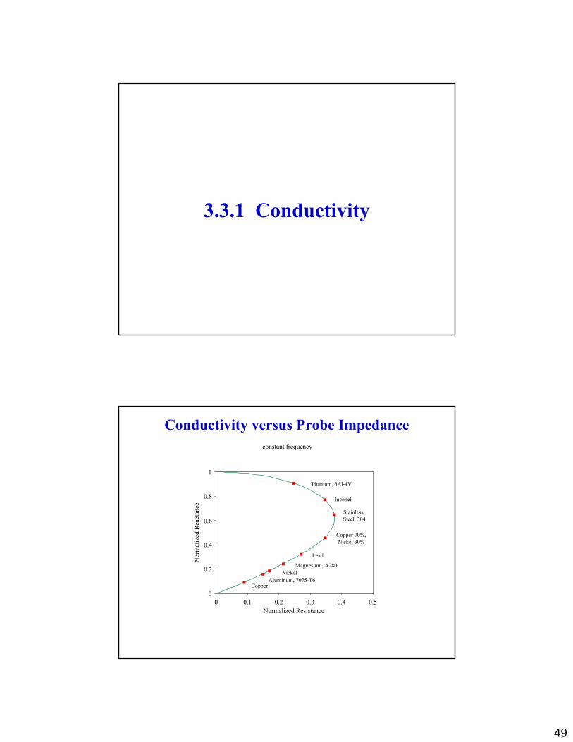
3.3.1 Conductivity
Conductivity versus Probe Impedance constant frequency
0
0.2
0.4
0.6
0.8
1
0 0.1 0.2 0.3 0.4 0.5Normalized Resistance
Nor
mal
ized
Rea
ctan
ce
StainlessSteel, 304
CopperAluminum, 7075-T6
Titanium, 6Al-4V
Magnesium, A280
Lead
Copper 70%,Nickel 30%
Inconel
Nickel

50
Conductivity versus Alloying and Temper IACS = International Annealed Copper Standard
σIACS = 5.8×10⁷ Ω-1m-1 at 20 °C
ρIACS = 1.7241×10⁻⁸ Ωm
20
30
40
50
60C
ondu
ctiv
ity [%
IAC
S]
T3 T4
T6
T0
2014
T4
T6T0
6061
T6
T73T76
T0
70752024
T3 T4
T6
T72T8
T0
Various Aluminum Alloys
Apparent Eddy Current Conductivity
• high accuracy (≤ 0.1 %)
• controlled penetration depth
specimen
eddy currents
probe coil
magnetic field
0
0.2
0.4
0.6
0.8
1.0
0.10 0.2 0.3 0.4 0.5
lift-offcurves
conductivity
curve(frequency)
Normalized Resistance
Nor
mal
ized
Rea
ctan
ce
σ,
σ = σ2
σ = σ1
= 0
= s
1
23
4
Normalized Resistance
Nor
mal
ized
Rea
ctan
ce

51
Lift-Off Curvature
inductive(low frequency)
capacitive(high frequency)
“Horizontal” Component
“Ver
tical
”C
ompo
nent
lift-off
.
conductivity
σ2
σ1
σ
ℓ = s ℓ = 0
“Horizontal” Component
“Ver
tical
”C
ompo
nent
.
conductivity
lift-off
σ2
σ1
σ
ℓ = s ℓ = 0
Inductive Lift-Off Effect
-2.0
-1.5
-1.0
-0.5
0.0
0.5
1.0
1.5
2.0
0.1 1 10 100Frequency [MHz]
Rel
ativ
e ΔA
ECC
[%] .
-2.0
-1.5
-1.0
-0.5
0.0
0.5
1.0
1.5
2.0
0.1 1 10 100Frequency [MHz]
Rel
ativ
e ΔA
ECC
[%] .
63.5 μm50.8 μm38.1 μm25.4 μm19.1 μm12.7 μm6.4 μm0.0 μm
-100
1020304050607080
0.1 1 10 100Frequency [MHz]
AEC
L [μ
m]
.
-100
1020304050607080
0.1 1 10 100Frequency [MHz]
AEC
L [μ
m]
. .
63.5 μm50.8 μm38.1 μm25.4 μm19.1 μm12.7 μm6.4 μm0.0 μm
4 mm diameter 8 mm diameter
1.5 %IACS 1.5 %IACS
52
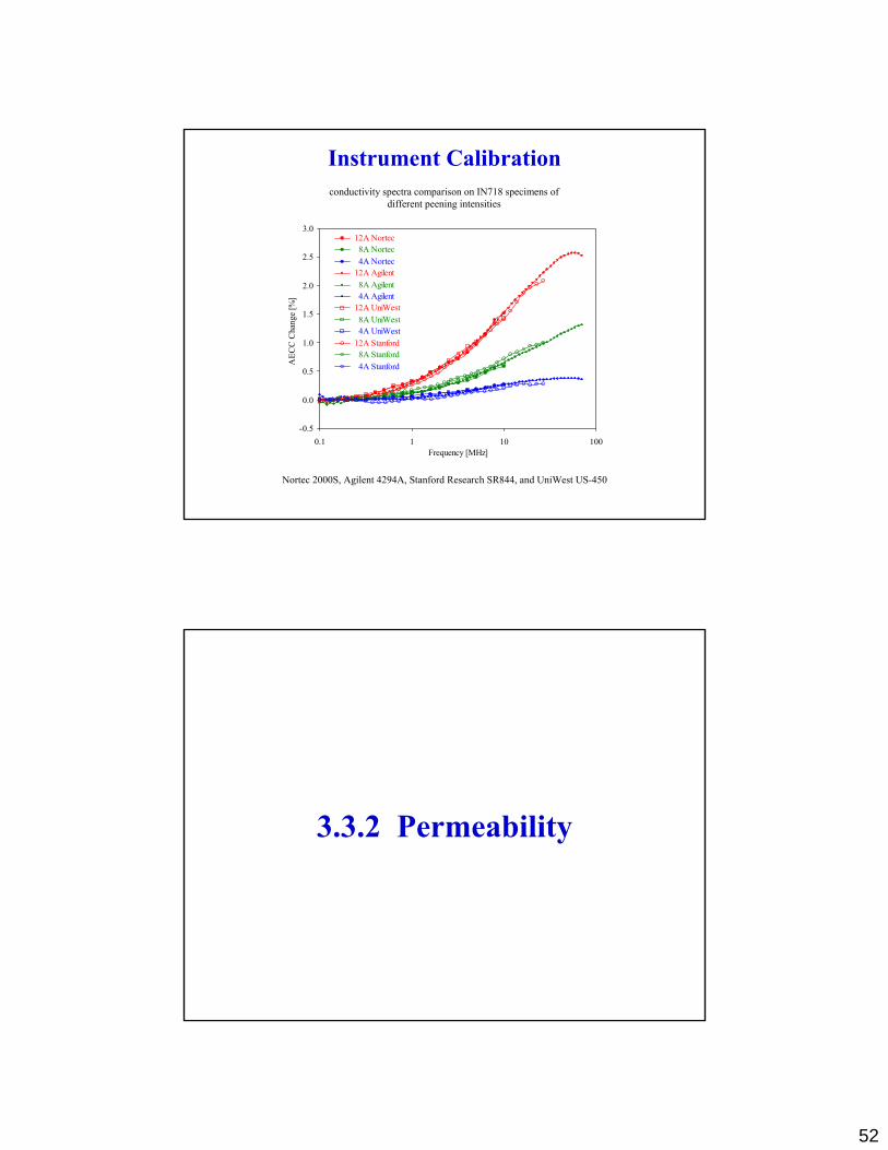
Instrument Calibration
-0.5
0.0
0.5
1.0
1.5
2.0
2.5
3.0
0.1 1 10 100Frequency [MHz]
AEC
C C
hang
e [%
] .
12A Nortec 8A Nortec 4A Nortec 12A Agilent 8A Agilent 4A Agilent 12A UniWest 8A UniWest 4A UniWest 12A Stanford 8A Stanford 4A Stanford
Nortec 2000S, Agilent 4294A, Stanford Research SR844, and UniWest US-450
conductivity spectra comparison on IN718 specimens of different peening intensities
3.3.2 Permeability

53
Magnetic Susceptibility
0
0.2
0.4
0.6
0.8
1.0
0.10 0.2 0.3 0.4 0.5
lift-off
frequency(conductivity)
Normalized Resistance
Nor
mal
ized
Rea
ctan
ce
permeability
Normalized Resistance
Nor
mal
ized
Rea
ctan
ce
0
1
2
3
4
0 0.2 0.4 0.6 0.8 1 1.2
2
3
1
µr = 4permeability
moderately high susceptibility low susceptibility
paramagnetic materials with small ferromagnetic phase content
increasing magnetic susceptibility decreases the apparent eddy current conductivity (AECC)
frequency(conductivity)
Magnetic Susceptibility versus Cold Work
10-4
10-3
10-2
10-1
100
101
0 10 20 30 40 50 60Cold Work [%]
Mag
netic
Sus
cept
ibili
ty
SS304L
IN276
IN718
SS305
SS304SS302
IN625
cold work (plastic deformation at room temperature) causesmartensitic (ferromagnetic) phase transformation
in austenitic stainless steels

54
3.3.3 Metal Thickness
Thickness versus Normalized Impedance
thickness loss due to corrosion, erosion, etc.
probe coil
scanning
0
0.2
0.4
0.6
0.8
1
0 0.1 0.2 0.3 0.4 0.5 0.6
thickplate
Normalized Resistance
Nor
mal
ized
Rea
ctan
ce
thinplate
lift-off
thinning
-0.2
0
0.2
0.4
0.6
0.8
1
0 1 2 3Depth [mm]
Re
F
f = 0.05 MHzf = 0.2 MHzf = 1 MHz
aluminum (σ = 46 %IACS)
/ /( ) x i xF x e e− δ − δ=

55
Thickness Correction
1.0
1.1
1.2
1.3
1.4
0.1 1 10Frequency [MHz]
Con
duct
ivity
[%IA
CS]
1.0 mm1.5 mm2.0 mm2.5 mm3.0 mm3.5 mm4.0 mm5.0 mm6.0 mm
thickness
Vic-3D simulation, Inconel plates (σ = 1.33 %IACS)
ao = 4.5 mm, ai = 2.25 mm, h = 2.25 mm
3.3.4 Coating Thickness

56
Non-conducting Coating
non-conductingcoating
probe coil, ao
t
d
ℓ
conducting substrate
ao > t, d > δ, AECL = ℓ + t
-100
1020304050607080
0.1 1 10 100Frequency [MHz]
AEC
L [μ
m]
-100
1020304050607080
0.1 1 10 100Frequency [MHz]
AEC
L [μ
m]
63.5 μm
50.8 μm
38.1 μm
25.4 μm
19.1 μm
12.7 μm
6.4 μm
0 μm
ao = 4 mm, simulatedlift-off:
ao = 4 mm, experimental
Conducting Coating
conductingcoating
probe coil, ao
t
d
ℓ
conducting substrate (µs,σs)
approximate: large transducer, weak perturbation
equivalent depth:
( )e1AECC( )
2 s sf
f
⎛ ⎞≈ σ δ = σ⎜ ⎟⎜ ⎟π μ σ⎝ ⎠
21( ) AECC
4 s sz
z
⎛ ⎞σ ≈ ⎜ ⎟⎜ ⎟π μ σ⎝ ⎠
se 2
δδ =
analytical: Fourier decomposition (Dodd and Deeds)
numerical: finite element, finite difference, volume integral, etc.(Vic-3D, Opera 3D, etc.)
zJe
z = δe

57
Simplistic Inversion of AECC Spectra
AEC
C C
hang
e [%
]
-0.2
0
0.2
0.4
0.6
0.8
1
1.2
0.001 0.1 10 1000
Frequency [MHz]
AEC
C C
hang
e [%
]-0.2
0
0.2
0.4
0.6
0.8
1
1.2
0.001 0.1 10 1000
Frequency [MHz]
Depth [mm]
Con
duct
ivity
Cha
nge
[%]
-0.2
0
0.2
0.4
0.6
0.8
1
1.2
0 0.2 0.4 0.6 0.8 1
input profile
inverted from AECC
uniform
Depth [mm]
Con
duct
ivity
Cha
nge
[%]
-0.2
0
0.2
0.4
0.6
0.8
1
1.2
0 0.2 0.4 0.6 0.8 1
input profile
inverted fromAECC
Gaussian
0.254-mm-thick surface layer of 1% excess conductivity
3.3.5 Flaw Detection

58
Impedance Diagram
Normalized Resistance
0
0.2
0.4
0.6
0.8
1
0 0.1 0.2 0.3 0.4 0.5
conductivity(frequency)
crackdepth
flawlessmaterialω1
lift-off
Nor
mal
ized
Rea
ctan
ce
ω2
apparent eddy current conductivity (AECC) decreasesapparent eddy current lift-off (AECL) increases
Crack Contrast and Resolution
probe coil
crack
0
0.2
0.4
0.6
0.8
1
0 1 2 3 4 5Flaw Length [mm]
Nor
mal
ized
AEC
C
semi-circular crack
-10% threshold
detectionthreshold
ao = 1 mm, ai = 0.75 mm, h = 1.5 mm
austenitic stainless steel, σ = 2.5 %IACS, μr = 1
Vic-3D simulation
f = 5 MHz, δ ≈ 0.19 mm
59
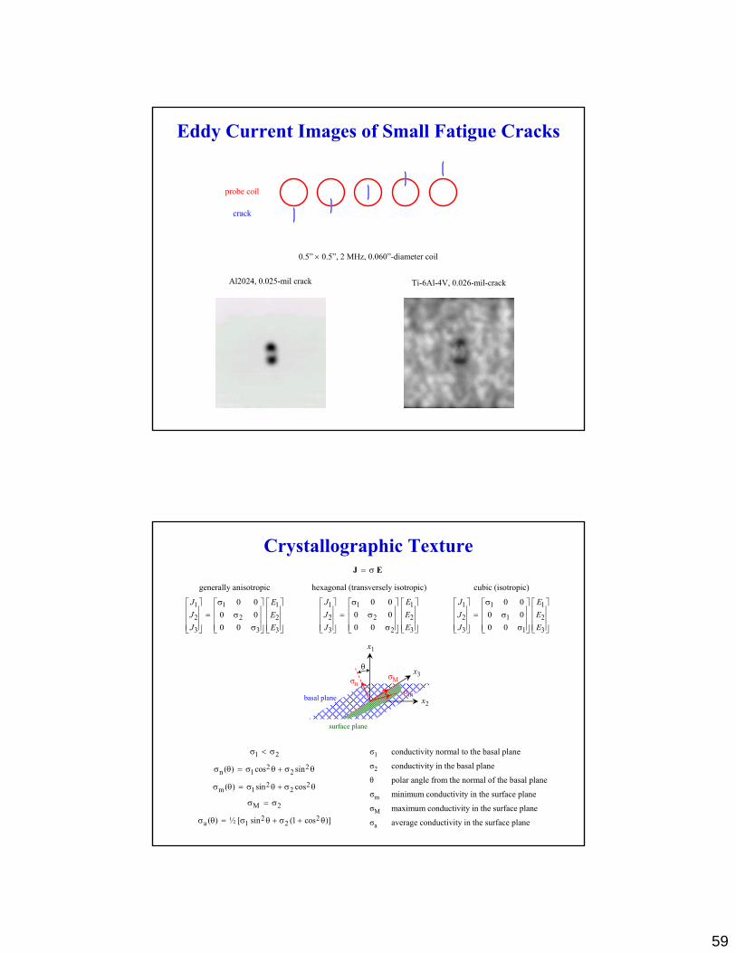
Eddy Current Images of Small Fatigue Cracks
Al2024, 0.025-mil crack Ti-6Al-4V, 0.026-mil-crack
0.5” × 0.5”, 2 MHz, 0.060”-diameter coil
probe coil
crack
Crystallographic Texture= σJ E
1 1 1
2 2 2
3 3 3
0 00 00 0
J EJ EJ E
σ⎡ ⎤ ⎡ ⎤ ⎡ ⎤⎢ ⎥ ⎢ ⎥ ⎢ ⎥= σ⎢ ⎥ ⎢ ⎥ ⎢ ⎥⎢ ⎥ ⎢ ⎥ ⎢ ⎥σ⎣ ⎦ ⎣ ⎦ ⎣ ⎦
generally anisotropic hexagonal (transversely isotropic)
1 1 1
2 2 2
3 2 3
0 00 00 0
J EJ EJ E
σ⎡ ⎤ ⎡ ⎤⎡ ⎤⎢ ⎥ ⎢ ⎥⎢ ⎥= σ⎢ ⎥ ⎢ ⎥⎢ ⎥⎢ ⎥ ⎢ ⎥⎢ ⎥σ⎣ ⎦⎣ ⎦ ⎣ ⎦
cubic (isotropic)
1 1 1
2 1 2
3 1 3
0 00 00 0
J EJ EJ E
σ⎡ ⎤ ⎡ ⎤⎡ ⎤⎢ ⎥ ⎢ ⎥⎢ ⎥= σ⎢ ⎥ ⎢ ⎥⎢ ⎥⎢ ⎥ ⎢ ⎥⎢ ⎥σ⎣ ⎦⎣ ⎦ ⎣ ⎦
σ1 conductivity normal to the basal plane
σ2 conductivity in the basal plane
θ polar angle from the normal of the basal plane
σm minimum conductivity in the surface plane
σM maximum conductivity in the surface plane
σa average conductivity in the surface plane2 2a 1 2( ) ½ [ sin (1 cos )]σ θ = σ θ + σ + θ
2 2n 1 2( ) cos sinσ θ = σ θ + σ θ
M 2σ = σ
1 2σ < σ
2 2m 1 2( ) sin cosσ θ = σ θ + σ θ
x1
x3
x2basal plane
θ
surface plane
σnσm
σM

60
Electric “Birefringence” Due to Texture
1.00
1.01
1.02
1.03
1.04
1.05
0 30 60 90 120 150 180Azimuthal Angle [deg]
Con
duct
ivity
[%IA
CS]
highly textured Ti-6Al-4V plate equiaxed GTD-111
1.30
1.32
1.34
1.36
1.38
1.40
0 30 60 90 120 150 180Azimuthal Angle [deg]
Con
duct
ivity
[%IA
CS]
500 kHz, racetrack coil
Grain Noise in Ti-6Al-4V
as-received billet material solution treated and annealed heat-treated, coarse
heat-treated, very coarse heat-treated, large colonies equiaxed beta annealed
1” × 1”, 2 MHz, 0.060”-diameter coil

61
Eddy Current versus Acoustic Microscopy
5 MHz eddy current 40 MHz acoustic
1” × 1”, coarse grained Ti-6Al-4V sample
InhomogeneityAECC Images of Waspaloy and IN100 Specimens
homogeneous IN100
2.2” × 1.1”, 6 MHz
conductivity range ≈1.33-1.34 %IACS
±0.4 % relative variation
inhomogeneous Waspaloy
4.2” × 2.1”, 6 MHz
conductivity range ≈1.38-1.47 %IACS
±3 % relative variation

62
Conductivity Material Noise
1.30
1.32
1.34
1.36
1.38
1.40
1.42
1.44
1.46
1.48
1.50
0.1 1 10Frequency [MHz]
AEC
C [%
IAC
S]
Spot 1 (1.441 %IACS)
Spot 2 (1.428 %IACS)
Spot 3 (1.395 %IACS)
Spot 4 (1.382% IACS)
as-forged Waspaloy
no (average) frequency dependence
Magnetic Susceptibility Material Noise1” × 1”, stainless steel 304
f = 0.1 MHz, ΔAECC ≈ 6.4 %
f = 5 MHz, ΔAECC ≈ 0.8 %
intact
f = 0.1 MHz, ΔAECC ≈ 8.6 %
f = 5 MHz, ΔAECC ≈ 1.2 %
0.51×0.26×0.03 mm3 edm notch

63
3.4 Special Example
Residual Stress Assessment
106102
intact (no residual stress)
with opposite residual stress
Fatigue Life [cycles]104 108
0
500
1000
1500
endurancelimit
service load
life timenatural
life timeincreasedA
ltern
atin
g St
ress
[MPa
]
Residual stresses have numerous origins that are highly variable.Residual stresses relax at service temperatures.

64
Surface-Enhancement TechniquesLow-Plasticity Burnishing (LPB)Shot Peening (SP) Laser Shock Peening (LSP)
Depth [mm]0 0.2 0.4 0.6 1.0 1.2
200
0
-200
-400
-600
-800
-1000
Res
idua
l Stre
ss [M
Pa]
SP Almen 12ASP Almen 4A
LSPLPB
Ti-6Al-4V
0 0.2 0.4 0.6 1.0 1.2Depth [mm]
Col
d W
ork
[%] 40
30
20
10
0
50
SP Almen 12ASP Almen 4A
LSPLPB
Ti-6Al-4V
Piezoresistive Effect
Electroelastic Tensor:
1 0 11 12 12 1
2 0 12 11 12 2
3 0 12 12 11 3
/ // // /
EEE
Δσ σ κ κ κ τ⎡ ⎤ ⎡ ⎤⎡ ⎤⎢ ⎥ ⎢ ⎥⎢ ⎥Δσ σ = κ κ κ τ⎢ ⎥ ⎢ ⎥⎢ ⎥⎢ ⎥ ⎢ ⎥⎢ ⎥Δσ σ κ κ κ τ⎣ ⎦⎣ ⎦ ⎣ ⎦
11 120/
/a
ipip E
Δσ ση = = κ + κ
τ
Isotropic Plane-Stress ( and ) :1 2 ipτ = τ = τ 3 0τ =
parallel, normal, circular
F F
δ
Adiabatic Electroelastic Coefficients:*11 11 thκ = κ + κ*12 1 2 thκ = κ + κ
-40-20
020406080
Time [1 s/div]
Axi
al S
tress
[ksi
]
Time [1 s/div]1.3971.3981.399
1.41.4011.4021.403
Con
duct
ivity
[%IA
CS]
IN 718, parallel

65
Material Types
parallel
-0.004
-0.002
0
0.002
0.004
-0.001 0 0.001 0.002τua / E
Δσ
/ σ0
normal
Copper
Ti-6Al-4V
parallel
-0.004
-0.002
0
0.002
0.004
-0.002 0 0.002 0.004τua / E
Δσ
/ σ0
normalparallel
-0.004
-0.002
0
0.002
0.004
-0.001 0 0.001 0.002τua / E
Δσ
/ σ0
normal
Al 2024
parallel
-0.004
-0.002
0
0.002
0.004
-0.001 0 0.001 0.002τua / E
Δσ
/ σ0
normal
Al 7075
Waspaloy
parallel
-0.004
-0.002
0
0.002
0.004
-0.002 0 0.002 0.004τua / E
Δσ
/ σ0
normal
IN718
parallel
-0.004
-0.002
0
0.002
0.004
-0.002 0 0.002 0.004τua / E
Δσ
/ σ0
normal
XRD and AECC Measurements
-2000
-1500
-1000
-500
0
500
0 0.2 0.4 0.6 0.8Depth [mm]
Res
idua
l Stre
ss [M
Pa]
Almen 4AAlmen 8AAlmen 12AAlmen 16A
-1
0
1
2
3
0.1 1 10Frequency [MHz]
Con
duct
ivity
Cha
nge
[%] Almen 4A
Almen 8AAlmen 12AAlmen 16A
0
10
20
30
40
50
0 0.2 0.4 0.6 0.8
Col
d W
ork
[%]
Almen 4AAlmen 8AAlmen 12AAlmen 16A
Depth [mm]
before (solid circles) and after full relaxation for 24 hrs at 900 °C (empty circles)
-2000
-1500
-1000
-500
0
500
0 0.2 0.4 0.6 0.8Depth [mm]
Res
idua
l Stre
ss [M
Pa]
Almen 4AAlmen 8AAlmen 12AAlmen 16A
0
10
20
30
40
50
0 0.2 0.4 0.6 0.8
Col
d W
ork
[%]
Almen 4AAlmen 8AAlmen 12AAlmen 16A
Depth [mm]
-1
0
1
2
3
0.1 1 10Frequency [MHz]
Con
duct
ivity
Cha
nge
[%] Almen 4A
Almen 8AAlmen 12AAlmen 16A
Waspaloy

66
Thermal Stress Relaxation in WaspaloyWaspaloy, Almen 8A, repeated 24-hour heat treatments at increasing temperatures
0.1 0.16 0.25 0.4 0.63 1 1.6 2.5 4 6.3 10
Frequency [MHz]
0
0.1
0.2
0.3
0.4
0.5
0.6
App
aren
t Con
duct
ivity
Cha
nge
[% ] intact
300 °C350 °C400 °C450 °C500 °C550 °C600 °C650 °C700 °C750 °C800 °C850 °C900 °C
The excess apparent conductivity gradually vanishes during thermal relaxation!
XRD versus Eddy Current
-0.2
0.0
0.2
0.4
0.6
0.8
1.0
1.2
0.01 0.1 1 10Frequency [MHz]
AEC
C C
hang
e [%
]
eddy current
0.0 0.5 1.0 1.5Depth [mm]
Col
d W
ork
[%]
.
0
5
10
15
20XRD
.
-1400
-1200
-1000
-800
-600
-400
-200
0
200
0.0 0.5 1.0 1.5Depth [mm]
Res
idua
l Stre
ss [M
Pa]
eddy currentXRD
inversion of measured AECC in low-plasticity burnished Waspaloy

67
0
10
20
30
40
0 0.1 0.2 0.3 0.4 0.5 0.6 0.7Depth [mm]
Col
d W
ork
[%]
.
Almen 4A (XRD) Almen 8A (XRD) Almen 12A (XRD)
-1800-1600-1400-1200-1000
-800-600-400-200
0200
0 0.1 0.2 0.3 0.4 0.5 0.6 0.7Depth [mm]
Res
idua
l Stre
ss [M
Pa]
.
Almen 4A (AECC) Almen 8A (AECC) Almen 12A (AECC) Almen 4A (XRD) Almen 8A (XRD) Almen 12A (XRD)
≈ 50 MHz
XRD versus High-Frequency Eddy Currentshot peened IN100 specimens of Almen 4A, 8A and 12A peening intensity levels

68
4 Magnetic NDE
4.1 Magnetic Properties
4.2 Magnetic Measurements
4.3 Magnetic Materials Characterization
4.4 Magnetic Flaw Detection
4.1 Magnetic Properties
69
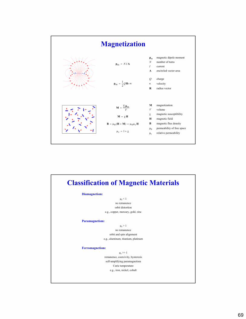
Magnetization
M magnetizationV volumeχ magnetic susceptibility
H magnetic field
B magnetic flux density
μ0 permeability of free space
μr relative permeability
pm magnetic dipole momentN number of turnsI currentA encircled vector area
m N I=p A
+I -I
mV
∑=pM
= χM H
0 0 r( )= μ + = μ μB H M H
r 1μ = + χ
m12
Q= ×p R v
Q charge
v velocity
R radius vector
Classification of Magnetic MaterialsDiamagnetism:
μr < 1no remanenceorbit distortion
e.g., copper, mercury, gold, zinc
Paramagnetism:μr > 1
no remanenceorbit and spin alignment
e.g., aluminum, titanium, platinum
Ferromagnetism:μr >> 1
remanence, coercivity, hysteresisself-amplifying paramagnetism
Curie temperaturee.g., iron, nickel, cobalt

70
Diamagnetism
pm magnetic dipole momentpspin electron spinporb electron orbital motionN number of turns
I current
A encircled area
e charge of proton
τ orbital period
r orbital radius
v orbital velocity
Ei induced electric field
Fe decelerating electric force
m mass of electron
n dipoles within unit volume
χ magnetic susceptibility
vQ
Fm
B
vQFe
B
ieF e E=
mF ev B=
m orb spin= +p p p
2orb 2
Q A e r vp N I Ar
π= = = −
τ π
orb 2er vp = −
2 22 2 0orb 4 4
e re rp B Hm m
μΔ = − = −
ei2 2 Fd r E r
dt eΦ
− = π = − π
2d m dvrdt e dtΦ
= π
2 2 mB r r ve
π = π Δ
2erv Bm
Δ =
- χ ≈ 1-10 ppm
2 20orb 4
e rnm
μχ = −
Weak Paramagnetism, Curie Lawm orb spin= +p p p
pm magnetic dipole moment
B magnetic flux density
Fm magnetic force
Tm twisting moment or torque
Um potential energy of the dipole
kB Boltzmann constant
T absolute temperature
n dipoles within unit volume
χ magnetic susceptibility
m m= ×T p B
m mU = −p Bi
m m90 90
( ) sinU T d p B dθ θ
= θ θ = θ θ∫ ∫
m m cosU p B= − θ
m m sinT p B= θ
m m0
Bm( )U U
k Tp U e−
−=
20
B3n mM C
H k T Tμ
χ = = =
Curie Law:
χ ≈ 5-50 ppm
+I
-Ipm
Fm
B
Fm
Tm
θ

71
Strong Paramagnetism, Curie-Weiss Law:
t iH H H H M= + = + α
tCM HT
=
t i
M M MM TH H H MC
χ = = =− − α
Curie-Weiss law:C
CT T
χ =−
MH
χ =
M magnetization
H exciting magnetic field
χ magnetic susceptibility
C material constant
T absolute temperature
Ht total magnetic field
Hi interaction field
α material factor
TC Curie temperature
Curie law:CM HT
≈
CT C
χ =− α
CT
χ ≈
Ferromagnetism(i) magnetic polarization is produced by collective action of
similarly oriented spins within magnetic domains
(ii) very high permeability
(iii) magnetic hysteresis
(v) remnant magnetic polarization (remanence)
(vi) coercive magnetic field (coercivity)
(iv) depolarization above the (magnetic) Curie temperature
H
B
Br
Hc
first magnetization

72
Spontaneous Magnetization
N N N N
S S S S
N S N S
S N S N
N N S S
S S N N
[100]
[010] “easy” magnetic axis
[001]
[110]
[111]
total internal wall externalU U U U= + +
Magnetic Domains in Single Crystalseasy magnetic axes
H = 0
H
H
H
1 demagnetization(spontaneous magnetization)
4 technical saturation
3 “knee” of the magnetization curve
2 partial magnetization
domain wallmovement
irreversiblerotation
reversiblerotation
H
B
1
2
354
5 full saturation(no precession)
thermal precession not shown

73
4.2 Magnetic Measurements
Magnetic Sensors
10-2
10-1
100
101
102
103
104
105
0 5 10 15 20 25Frequency [Hz]
Flux
Den
sity
[pT/
Hz1/
2 ]
Hall
GMR
SDP
fluxgate
SQUID
noise threshold
axialdV N i N ABdtΦ
= − = − ωcoil:

74
Hall Detector
I I
a
b
xyz
x x
Bz
VH
FmFe
( )Q= + ×F E v B
( ) 0y y x zF e E v B= − + =
Hy
VEa
=
x xI en ab v= −
Hx
y x z zIV a E av B B
enb= = − =
HH
xz
R IV Bb
=
H1R
en=
Fluxgate
Iexc
Vsens
B1
B2
B
hard magnetic cores
high-frequencyexcitation
low-frequency or dcexternal magnetic field
B1 + B2
B2
B1
B1 + B2
B2
B1
B = 0 B ≠ 0
t
t
t
t
t
t
H
B
sensing voltage(to be low-pass filtered)

75
Vibrating-Sample Magnetometer
Vsens B0
vibration (ω)
0 sin( )d d t= ω
1 0 0( ) [ sin( )]t A B M tΦ = + μ κ ω
2 0 0( ) [ sin( )]t A B M tΦ = − μ κ ω
1 2sens( )V t N N
t t∂Φ ∂Φ
= − +∂ ∂
0
0
BM = χ
μ
sens 0( ) 2 cos( )V t N A B t= − ωχ κ ω
B0 bias magnetic flux density
M magnetization
χ magnetic susceptibility
µ0 permeability of free space
d specimen displacement
d0 specimen amplitude
ω angular frequency
t time
κ geometrical coupling factor
A coil cross section
Φ1,2 flux in coil 1 and 2
N number of turns
Vsens sensing voltage
Faraday Balance
Um magnetic potential energy
pm magnetic dipole moment
B magnetic flux density
M magnetization
V volume
Ug gravitational potential energy
U total potential energy
h height
W actual weight
W’ apparent weight
χ magnetic susceptibility
H magnetic field
µ0 permeability of free space
for a single dipole:
for a given magnetized volume:
precision scale
specimen
W’ = W - Fm
electromagnet
spacerh
m mU = −p Bi
g mU U U= +
' dU dBW W M Vdh dh
= = −
mU M V B= −
U W h M V B= −
M H= χ
200'
2VdH dHW W V H
dh dhμ
− = − μ χ = − χ

76
4.3 Magnetic Materials Characterization
Magnetic Properties
-1.5
-1
-0.5
0
0.5
1
1.5
-5 -4 -3 -2 -1 0 1 2 3 4 5Magnetic Field [kA/m]
Flux
Den
sity
[Tes
la]
hardened steel
soft iron
0 0( , ) ( , )p pB B H M H M H M= = μ + μferromagnetic materials:
para- and diamagnetic materials: 0 ( )B H M= μ +
M H= χ
0 rB H= μ μ
r 1μ = + χ

77
Initial Magnetizationanhysteretic initial magnetization curve
Flux Density
Differential Permeability
Magnetic FieldFl
ux D
ensi
ty
B magnetic flux density
H magnetic field
M magnetization
µ0 permeability of free space
µd differential permeability
M0 saturation magnetization
n dipoles per unit volume
pm magnetic dipole moment
ddBdH
μ =
0limH
M M→∞
=
0 ( )B H M= μ +
0 mM n p≤
Retentivity, Coercivity, Hysteresis
Br remanence [Vs/m2]
Mr remnant magnetization
µ0 permeability of free space
Hc coercive field [A/m]
Hci intrinsic coercivity
U0 magnetic energy density
A hysteresis area [J/m3]
0 ( )B H M= μ +
p( , )M M H M=
technical saturation:
HH
B
Br
Hc
r 0 rB M= μ
c c( ) 0H M H+ =
ci( ) 0M H =
c ciH H≤
0dU B dH=
0U AΔ =

78
Texture, Residual Stress
-2
-1
0
1
2
-300 -200 -100 0 100 200 300Magnetic Field [A/m]
Flux
Den
sity
[T]
σ = 0 MPa B||
B⊥
-2
-1
0
1
2
-300 -200 -100 0 100 200 300Magnetic Field [A/m]
Flux
Den
sity
[T]
σ = 36 MPa B||
B⊥
-2
-1
0
1
2
-300 -200 -100 0 100 200 300Magnetic Field [A/m]
Flux
Den
sity
[T]
σ = 183 MPaB||
B⊥
-2
-1
0
1
2
-300 -200 -100 0 100 200 300Magnetic Field [A/m]
Flux
Den
sity
[T]
σ = 110 MPa B||
B⊥
mild steel (Langman 1985)
Magnetostriction
Induced magnetostriction:
Ms spontaneous magnetization
M0 saturation magnetization
e spontaneous strain within a single domain
ε1,2,3 principal strains
H
123e
ε =
12,3 2 3
eεε = − = −
1 2 eε − ε =
Spontaneous magnetostriction:
easy magnetic axes
H = 0
domains 0M M M= ≤
domain domain1 2,3, 0eε = ε =
volume1,2,3 3
eε =
volume 0M ≈

79
Barkhausen Noise
H = 0
H
domain wallmovementH
B
magnetic field Barkhausen noise
Am
plitu
de
Time
• magnetic Barkhausen noise• acoustic Barkhausen noise
Curie Temperature
ferromagnetic materials (T < TC):
0.0
0.2
0.4
0.6
0.8
1.0
1.2
0.0 0.2 0.4 0.6 0.8 1.0 1.2 1.4T / TC
Ms
/ M0
typical pure metal
typical alloy
χ magnetic susceptibility
C material constant
T temperature
TC Curie temperature
Curie-Weiss law:C
CT T
χ =−

80
4.4 Magnetic Flaw Detection
Magnetic Flux Leakage
Advantages:
fast
inexpensive
large, awkward shaped specimens (particle)
Disadvantages:
material sensitive
poor sensitivity
poor penetration depth
ferromagnetic test piece
sensor
Hall cell, etc.)(small coil,
exciter coil

81
Magnetic Boundary Conditions
xt
medium I
medium II
BIθΙ
boundary
BII
BII,t
BII,n
θΙΙ
BI,n
BI,t
xn
xt
medium I
medium II
HI
θΙ
HII
HII,t
HII,n
θΙΙ
HI,n
HI,t
xn
Ampère's law:
∇× =H J
Gauss' law:
0∇ =Bi
I,n II,nB B= I,t II,tH H=
I I,n II II,nH Hμ = μ I I,n II II,ntan tanH Hθ = θ
I III II
tan tanθ θ=
μ μ
Magnetic Refraction
I III II
tan tanθ θ=
μ μ
µI/µII = 1030
100
0 15 45 60 75 900
15
30
45
60
75
90
30Ferromagnetic Angle, θI [deg]
Non
mag
netic
Ang
le, θ
II[d
eg]
medium I(ferromagnetic)
BI
BIIθΙΙ
θΙ
medium II(air)
medium I(ferromagnetic)
BI
BII
θΙΙ
θΙ
medium II(air)

82
Exciter Magnets
electromagnet
air gap
ferromagnetic core
H d N I MMF= =∫
0 r H AΦ = μ μ
0 rMMF d
AΦ
= ∫μ μ
mMMFR =
Φ
m0 r 0 r
1 1 ii i i
dRA A
= ≈ ∑∫μ μ μ μ
H magnetic field
N number of turns
I excitation current
MMF magnetomotive force
Φ magnetic flux
ℓ length of flux line
µ0 µr magnetic permeability
A cross section area
Rm magnetic reluctance
Yoke Excitation
Detection Methods:
• magnetic particle(gravitation, friction, adhesion,cohesion, magnetization)
• magnetic particle with ultraviolet paint
• coil
• Hall detector, GMR sensor
• fluxgate, etc.
Lateral Position
Tang
entia
l Mag
netic
Fie
ld
Lateral Position
Nor
mal
Mag
netic
Fie
ld
electromagnet
crack
N I
magnetometer

83
Subsurface Flaw Detection
H
B
1
2
saturation greatly reduces the differential permeability
crack
low magnetic field
crack
high magnetic field

84
5 Current Field Measurement
5.1 Alternating Current Field Measurement
5.2 Direct Current Potential Drop
5.3 Alternating Current Potential Drop
5.1 Alternating Current Field Measurement

85
Principle of Operation
electric field
magneticflux
density
axial (x)
transverse (y)
normal (z)
galvanic current injection
≈
magnetometer
magnetic injection:
primary ac flux
~~
Bx0
Field Perturbation
magneticflux
density
magnetometer
axial (x)
transverse (y)
normal (z)
axial flaw
cw current
Bz < 0
electriccurrent
Bz > 0
ccw current
axial scanningabove flaw Axial Position
B z[a
.u.]
Axial Position
B x[a
.u.]
B z[a
.u.]
Bx [a.u.]

86
Uniform Field
advantages:
• testing through coatings
• depth information
• limited boundary effects
disadvantages:
• reduced sensitivity
• sensitivity to geometry
• flaw orientation
effect of coating thickness on axial magnetic flux density Bx(ferrous steel, 5 kHz, δ ≈ 0.25 mm, 30-mm-long solenoid)
8
7
6
5
4
3
2
1
00 5 10 15 20
Coating Thickness [mm]
ΔBx
[%]
50 × 5 mm20 × 2 mm20 × 1 mm
slot size
30
25
20
15
10
5
0
Slot Depth [mm]
ΔBx
and
ΔB z
[%]
0 0.5 1 1.5 2 2.5
Bx at 5 kHzBz at 5 kHzBx at 50 kHzBz at 50 kHz
Axial Flaw
8
7
6
5
4
3
2
1
00 10 20 30 40
Slot Depth [mm]
ΔBxm
per 1
mm
Slo
t Dep
th [
%]
40-mm-longsolenoid
12-mm-longsolenoid
rate of increase of the minimum of Bx with slot depth at the center
2-mm-diameter coil, ferrous steel
changes normalized to Bx0
(parallel to B, normal to E)

87
Flaw Orientation
0.17
0.16
0.15
0.14
0.13
0.12
0.11
B x[T
]
0 1 2 3 4 5Scanning time [a. u.]
transverse flaw(normal to B)
axial flaw(normal to E)
0.025
0.020
0.150
0.100
0.05
0
-0.05
B z[T
]
0 1 2 3 4 5Scanning Time [a. u.]
transverse flaw(normal to B)
axial flaw(normal to E)
eddy current mode
magnetic flux mode
Magnetic Flux Mode
electromagnet
crack
N I
magnetometer
Lateral Position
Tang
entia
l Mag
netic
Fie
ld
Lateral Position
Nor
mal
Mag
netic
Fie
ld

88
5.2 Direct Current Potential Drop
Inductive versus Galvanic Coupling
specimen
eddy currents
probe coil
magnetic field
electric current
VI I
injectioncurrent
potential drop
specimen
advantages of galvanic coupling
dc and low-frequency operation
constant coupling (four-point measurement)
awkward shapes
absolute measurements
inherently directional

89
Thin-Plate Approximationcombined electric current and potential field2a
2b
t << a
( ) ( )2
IE r J rr tρ
= ρ =π
( ) ( )2r r
I drV r E r drt r
∞ ∞ρ= =∫ ∫
π
( ) ln const2IV r r
tρ
= − +π
( ) ( )V V V+ −Δ = −
lnI a bVt a bρ +
Δ =π −
[ ]2 ( ) ( )V V a b V a bΔ = − − +
I (+) I (-)V (+) V (-)
I (+) I (-)
V (+) V (-)
Lateral Spread of Current Distribution
( )2
IJ rr t
=π
(0,0) IJat
=π
2 2 2 22(0, )
2
I aJ wa w t a w
=π + +
2 2(0, )( )
I aJ wa w t
=π +
2
(0,0) 2(0, )J
J w=
2 22
22
(0,0) 2(0, )
a wJJ w a
+= =
2w a=
2w I (+) I (-)
V (+) V (-)
x
y
2a
J(0,w)
J(0,0)

90
Thick-Plate Approximation
2( ) ( )2
IE r J rrρ
= ρ =π
2( ) ( )2r r
I drV r E r drr
∞ ∞ρ= =∫ ∫
π
( ) const2IV r
rρ
= +π
t >> a
2a2b
I (+) I (-)V (+) V (-)
≈
combined electric current and potential field
I (+) I (-)V (+) V (-)
( ) ( )V V V+ −Δ = −
1 1IVa b a b
⎡ ⎤ρΔ = −⎢ ⎥π − +⎣ ⎦
[ ]2 ( ) ( )V V a b V a bΔ = − − +
Finite Plate Thickness
2a2b
t
2 2 1/ 2( )2 [ (2 ) ]n
IV rr nt
∞
= −∞
ρ= ∑
π +
2 2 1/ 2
2 2 1/ 2
1[( ) (2 ) ]
1[( ) (2 ) ]
n
IVa b nt
a b nt
∞
= −∞
⎡ρΔ = ∑ ⎢π − +⎣
⎤− ⎥+ + ⎦
I (+) I (-)
V (+) V (-)
n = 0
n = -1
n = +1
n = -2
n = +2
2t
I (+) I (-)V (+) V (-)
91
Resistance versus Thickness
0
1lim lnt
a bt a b→
+Λ =
π −2 2
2limt
ba b→∞
Λ =π −
VRI
Δ= = ρΛ
0.1
1
10
0.01 0.1 1 10 100Normalized Thickness, t / a
Nor
mal
ized
Res
ista
nce,
Λ
finite thicknessthin-plate appr.thick-plate appr.
a = 3b
Crack Detection by DCPDintact specimen
I (+) I (-)V (+) V (-)
( ) ( )0V V V+ −− = Δ
t
I (+) I (-)V (+) V (-)
cracked specimen
( ) ( )cV V V+ −− = Δ
c
1
2
3
0 0.2 0.4 0.6 0.8 1Normalized Crack Depth, c / t
Nor
mal
ized
Pot
entia
l Dro
p, Δ
V c/ Δ
V 0
a / t =0.441.21.8
a = 3b
infinite slot

92
Technical Implementation of DCPD
• low resistance, high current
• thermoelectric effect, pulsed, alternating polarity
• control of penetration via electrode separation
• low sensitivity to near-surface layer
• no sensitivity to permeability
powersupply
polarityswitch
+_
specimen
electrodesVs
+_
5.3 Alternating Current Potential Drop

93
Direct versus Alternating CurrentDCPD
ACPD
• higher resistance, lower current
• no thermoelectric effect
• control of penetration via frequency
• higher sensitivity to near-surface layer
• sensitivity to permeability
Thin-Plate/Thin-Skin Approximation
0lim lnf
V a bI t a b→
Δ ρ +=
π −
2a2b
t << aI (+) I (-)V (+) V (-)
Re lnV a bI T a b
Δ ρ +⎧ ⎫ ≈⎨ ⎬ π −⎩ ⎭
min ,T t≈ δ
fρ
δ =π μ
lim Re lnf
V f a bI a b→∞
Δ ρμ +⎧ ⎫ ∝⎨ ⎬ π −⎩ ⎭

94
Skin Effect in Thin Nonmagnetic Plates
t( )f f tδ = ≈
t 20
1ft
=πμ σ
analytical prediction
a = 20 mm, b = 10 mm, t = 2 mm
100
101
102
103
100 101 102 103 104 105
Frequency [Hz]
Res
ista
nce
[µΩ
]
1 %IACS2 %IACS5 %IACS
10 %IACS20 %IACS50 %IACS
100 %IACS
ft
a = 20 mm, b = 10 mm, σ = 50 %IACS
0.05 mm0.1 mm0.2 mm0.5 mm
1 mm2 mm5 mm
ft100
101
102
103
100 101 102 103 104 105
Frequency [Hz]
Res
ista
nce
[µΩ
]
Skin Effect in Thick Nonmagnetic Plates304 austenitic stainless steel, σ = 2.5 %IACS, experimental
101
102
103
104
100 101 102 103 104 105
Frequency [Hz]
Res
ista
nce
[µΩ
]
50 mm
20 mm
10 mm
6.25 mm
2.5 mm
2 mm
1 mm
0.5 mm
0.2 mm
0.1 mm
0.05 mm
a = 10 mm, b = 7.5 mm

95
Current Distribution in Ferritic Steelf = 0.1 Hz
FE predictions (Sposito et al., 2006)
f = 50 Hz
f = 1 kHz
a = 10 mm, b = 5 mm, t = 38-mm, c = 10 mm (0.5-mm-wide notches, two separated by 5 mm)
Thin-Skin ApproximationVZ R i XI
Δ= = +
c 0 c 0c
0 0
R RK
R− Γ − Γ
= ≈Γ
0 ln a ba b
+Γ =
− c2ln a b c
a b+ +
Γ =−
*0 0R R≈ Γ *
c cR R≈ Γ
0
1
2
1 2 3Electrode Shape Factor, a / b
Elec
trode
Gai
n, Γ
0
2b2a
2b2a
c
0 ln a bRa b
ρ +≈
πδ −2lnc
a b cRa b
ρ + +≈
πδ −
c0 0
1 2limc
cKa b→
≈Γ +
* fR μρ=
π

96
Technical Implementation of ACPD
low-passfilter
low-passfilter
oscillator differentialdriver
+_
90º phaseshifter
A/Dconverter
specimen
electrodesPC
processor
Vr
Vs
Vq
frequency range: 0.5 Hz - 100 kHz
driver current: 10-200 mA
resistance range: 1-10,000 µΩ
common mode rejection: 100-160 dB .
a = 0.160”
b = 0.080”w = 0.054”
2 d = 0.120”
voltagesensing
currentinjection
welding
weldment
d
w
edge weld
clamshellcatalytic converter
Application Example: Weld Penetration
NDE [mil]
Frac
ture
Sur
face
[mils
]
01020304050607080
0 10 20 30 40 50 60 70 80
weld penetration (w)
Weld Penetration [mil]
Res
ista
nce
[µΩ
]
0
50
100
150
200
0 20 40 60 80 100 120
b = 120 mils
80 mils100 mils
electrode separation (b)

97
Application Example: Erosion Monitoring
0 5 10 15 20Time [day]
20
21
22
23
24
25
Tem
pera
ture
[ºC
]
32.0
32.2
32.4
32.6
32.8
33.0
Res
ista
nce
[µΩ
]
0 5 10 15 20Time [day]
20
21
22
23
24
25
Tem
pera
ture
[ºC
]32.0
32.2
32.4
32.6
32.8
33.0
Res
ista
nce
[µΩ
]
erosionerosion
before compensation after compensation
β ≈ 0.001 [1/ºC]
0 0( ) [1 ( )]T T Tρ ≈ ρ + β −
5060708090
100110120130
0 200 400 600 800Temperature [ºC]
Res
istiv
ity [µ
Ωcm
]
301302303304309310316321347403
internalerosion/corrosion
pipe
98
6 Special Methods
6.1 Microwave Techniques
6.2 Dielectric Measurements
6.3 Thermoelectric Measurements
6.1 Microwave Techniques

99
Electromagnetic Spectrum
34 19, 6.63 10 Js, 1.6 10 CE h eV h e− −= ν = ≈ × ≈ ×
microwave
IR light
cosmic rays
X-rays
γ rays
UV light
visiblelight
radio frequency
Frequency [Hz]
10 1081064 10 1014101210 10 1020101816 1022 1024
Energy [eV]
10 10-610-8-10 10 10010-2-4 10 1061042 108 1010
Wavelength [m]
10 1001024 10 10-610-4-2 10 10-1210-10-8 10-14 10-16
typical lattice constant
Electromagnetic WavesPlane waves:
in dielectrics:
( )0
i t k xy y yE E e ω −= =E e e ( )
0i t k x
z z zH H e ω −= =H e e
0
0
E iH i
ωμη = =
σ+ ωε
( )k i i= − ωμ σ + ωε
in conductors:
/ ( / )0
x i t xyE e e− δ ω − δ=E e
/ ( / )0
x i t xzH e e− δ − ω − δ=H e
1 ik = −δ δ
1i iωμ +η = =
σ σδ
1f
δ =π μσ
00
0377μ
η = ≈ Ωε
0 0
0 r nμ η
η = ≈ε ε
( / )0
i t x cyE e ω −=E e
( / )0
i t x czH e ω −=H e
kcω
=
0
0 0
1
r
ccn
= =μ ε ε
80
0 0
1 3 10 m/sc = ≈ ×μ ε

100
Reflection/Transmission between Dielectrics
x
y
incident
reflected transmitted
I dielectric II dielectric
0 0I II
I II,
n nη η
η = η =
• strong penetration
• perceivable reflection
I III II
n nRn n
−=
+
Reflection from Conductors
x
y
incident
reflected transmitted“diffuse” wave
I dielectric II conductor
1 0f
δ = ≈π μσ
0II I
in
ηωμη = << η =
σ
II III I
1R η − η= ≈ −
η + η
• negligible penetration
• almost perfect reflection with phase reversal

101
Far-Field Measurement Configurations
detectorisolatoroscillatorcirculator
hornantenna
specimen
reflection (monostatic radar, pulse-echo)
detector
isolatoroscillator
hornantenna
specimen
transmission (bistatic radar, pitch-catch) scattering (bistatic radar, pitch-catch)
isolatoroscillator
hornantenna
specimen
detector detec
tor
Near-Field Inspection
detectorisolatoroscillatorcirculator
open-endedwaveguidespecimen stand-off
distance
air backing
foam coreadhesivesubstrateskin laminate
corrosion damage
coating
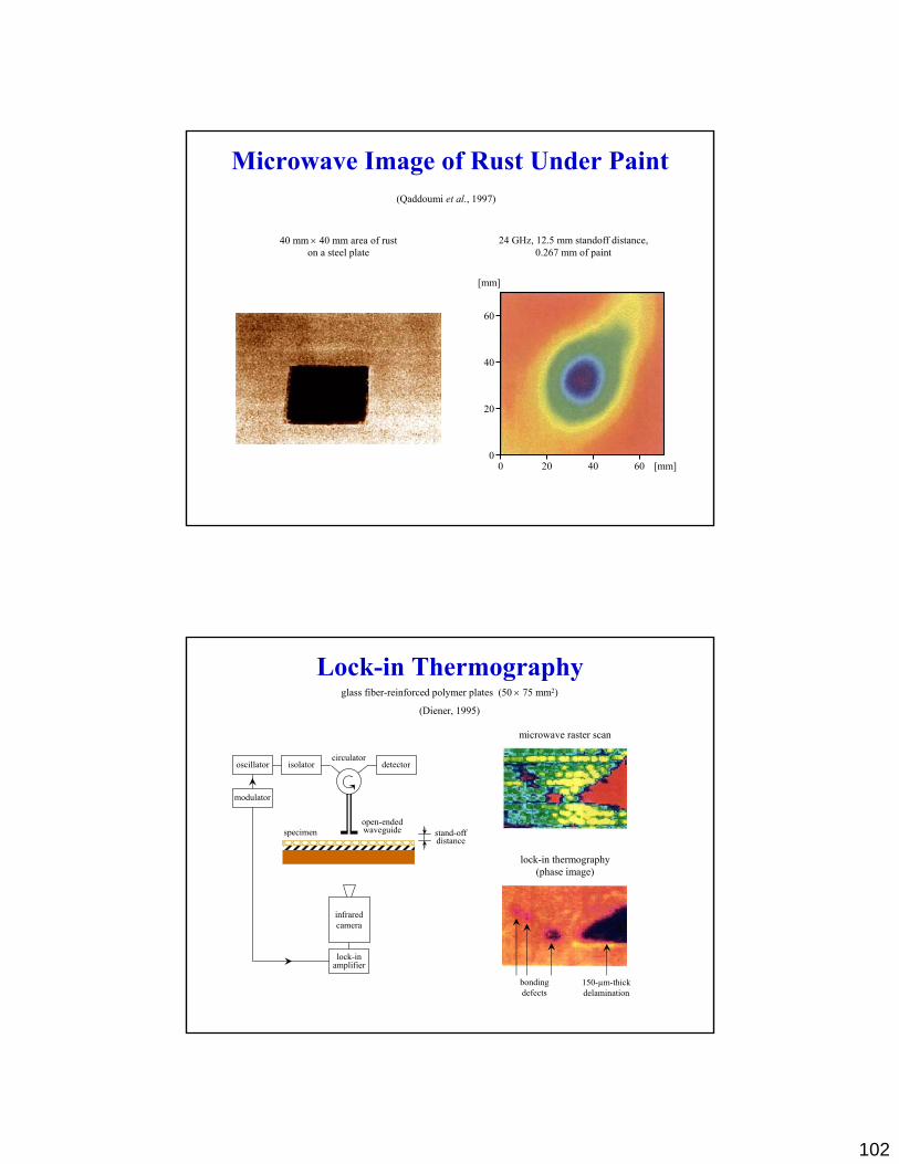
102
(Qaddoumi et al., 1997)
Microwave Image of Rust Under Paint
40 mm × 40 mm area of rust on a steel plate
24 GHz, 12.5 mm standoff distance, 0.267 mm of paint
60
40
20
06040200 [mm]
[mm]
Lock-in Thermographyglass fiber-reinforced polymer plates (50 × 75 mm2)
(Diener, 1995)
detectorisolatoroscillatorcirculator
open-endedwaveguidespecimen stand-off
distance
infraredcamera
lock-inamplifier
modulator
microwave raster scan
lock-in thermography(phase image)
150-µm-thickdelamination
bondingdefects

103
6.2 Dielectric Measurements
Fundamentals
t∂
∇× = +∂DH J
t∂
∇× = −∂BE
Maxwell's Equations:
Harmonic solution:
i iωε = σ + ωε
t∂
∇× = σ + ε∂EH E
t∂
∇× = −μ∂HE
i∇× = ωεH E
i∇× = − ωμE H
i σε = ε −
ω
= σJ E
= εD E
= μB H
E electric field
H magnetic field
D electric flux density
B magnetic flux density
J electric current density
σ electric conductivity
ε electric permittivity
µ magnetic permeability
complex electric permittivity
ω angular frequency
t time
ε

104
Electric Polarizatione dQ Q d= =p d e
+Q -Q +Q -Q
E
FeFe
e e= ×T p Ee tQ=F E
E
0= ε +D E P
ee 0V
∑= = χ εpP E
P electric polarization
pe electric dipole moment
V volume
χe electric susceptibility
ε0 permittivity of free space
dipole formation dipole rotation
0 r= ε εD E
r e1ε = + χ
Capacitance
QDA
ACDE
V E
⎫≈ ⎪⎪ ε⎪ ≈⎬= ⎪ε⎪⎪≈ ⎭
Q CV= dQ dVI Cdt dt
= =1V I dtC
= ∫
0 rε = ε ε
Y i C G= ω +
1Zi C
=ω
Y i C= ω
AG = σ
Y i C= ω
( ) '( ) ''( )iε ω = ε ω − ε ω
E
Q A
I
ideal dielectric lossy dielectric
( ) i σε ω = ε −
ω
conducting dielectric
Y i C= ω
AC = ε
''( )tan'( )
D ε ω= δ =
ε ω

105
Complex Electric Permittivity( ) '( ) ''( )iε ω = ε ω − ε ω
frequency [Hz]
Elec
tric
Perm
ittiv
ity [a
. u.]
+
_
ε’
ε’’
_
+dipolar
+
_
+
atomicresonance electronic
resonance
ionic
103 106 109 1012 1015 1018
_
's s0 0lim ( ) lim i
ω→ ω→
σε = ε ω = ε −
ω
Capacitive Probesparallel plate electrodes
sensor with guard electrodes
Vg
basic sensor
Rg
≈
Vm
Im
stray field electrodes
Vg
Rg
≈
Vm
≈Vm
Im×1
buffer

106
Auto-Balancing Bridge
Vg
Rg
≈
Im
H
deviceundertest L
+
_
RrefIm
high-gainoperationalamplifier
2 m refV I R=
1 m dutV I Z=
1dut ref
2
VZ R
V=
1V 2V
dutZ
vectorvoltmeter
vectorvoltmeter
“virtual”ground
Woven Composite
0
10
20
30
40
0.1 1 10 100Frequency [kHz]
Cap
acita
nce
[pF]
.
coateduncoated
0.001
0.01
0.1
1
10
0.1 1 10 100Frequency [kHz]
Con
duct
ance
[μS]
.
coateduncoated
conductive cloth for electric shielding

107
Adhesively Bonded CompositePethrick et al., 2002
0 0.5 1.0 1.5 2.0 2.5Water Uptake [%]
Thic
knes
s Var
iatio
n [%
]
2.5
2.0
1.5
1.0
0.5
0.00 10 20 30 40 50 60 70 80
Time1/2 [hr1/2]
Wat
er U
ptak
e [%
]
2.5
2.0
1.5
1.0
0.5
0.0
intact122 hr580 hr
1,007 hr1,590 hr5,350 hr
Frequency [Hz]
Rel
ativ
e Pe
rmitt
ivity
50
40
30
20
10
010-1 100 101 102 103 104 105 106 107 108 109
Frequency [Hz]
Die
lect
ric L
oss
103
102
101
100
10-1
10-2
10-1 100 101 102 103 104 105 106 107 108 109
intact122 hr580 hr
1,007 hr1,590 hr5,350 hr
6.3 Thermoelectric Measurements

108
Thermoelectric EffectSeebeck, Peltier, and Thomson effect: coupled electric and thermal flux
J electric current density
h thermal flux density
σ electric conductivity (∇T = 0)
κ thermal conductivity (∇V = 0)
V voltage
T temperature
S thermoelectric power
closed-circuit Seebeck effect:
hA
T1 T2
A
B hB
JA
JB
I
open-circuit Seebeck effect:
T1 T2
A
B
hA
hB
JA = 0
JB = 0
VS
T0 T0V+ _
S VS T Tσ σ −∇⎡ ⎤ ⎡ ⎤ ⎡ ⎤
=⎢ ⎥ ⎢ ⎥ ⎢ ⎥σ κ −∇⎣ ⎦ ⎣ ⎦ ⎣ ⎦
Jh
V= − σ∇JT= − κ∇h
( )V S T= − σ ∇ + ∇ =J 0 V S T∇ = − ∇
01 2
0 1 2S B A B
TT T
T T TV S dT S dT S dT= + +∫ ∫ ∫
2 2
1 1S A B AB( )
T T
T TV S S dT S dT= − =∫ ∫
Absolute Thermoelectric Power
Temperature [K]0 500 1000 1500
-40
-30
-20
-10
0
10
20
30
Ther
moe
lect
ric P
ower
[µV
/K] W (tungsten)
Mo (molybdenum)
Ag (silver)
Cu (copper)
Au (gold)
Pt (platinum)
Pd (palladium)
2 2
1 1S A B AB( )
T T
T TV S S dT S dT= − =∫ ∫
S AB 2 1( )V S T T≈ −

109
Contact Thermoelectric Tester
Primary Effect:
• chemical composition
Secondary Effects:
• anisotropy, texture
• fatigue, cold work, plasticity, residual stress, etc.
open-circuit Seebeck effect
specimen (A)
electrical heating
“cold” junction “hot” junction
referenceelectrodes
(B)
~~
V+ _
TEP versus Chemical Composition
Ag Content [%]
20
0
-20
-40
-60
Ther
moe
lect
ric P
ower
[µV
/K]
0 20 40 60 80 100
273 K83 K
Ag Content [%]
50
40
30
20
10
0
Elec
tric
Res
istiv
ity [µ
Ωcm
]
0 20 40 60 80 100
293 K4.2 K
palladium-silver binary alloy
(Rudnitskii, 1956)

110
TEP Anisotropy
hexagonal single crystal
Zinc, relative to basal plane
(Rowe and Schroeder, 1970)
Temperature [K]
-3
-2
-1
0
1
2
3
0 50 100 150 200 250 300
perpendicular
parallelTh
erm
oele
ctric
Pow
er [µ
V/K
]
TEP versus Texturecold-worked polycrystalline material
Ti-6Al-4V, relative to cold work direction
(Carreon and Medina, 2006)
50 µm
before annealing after annealing
0 30 60 90 120 150 180Azimuthal Angle [deg]
-5.1
-5.0
-4.9
-4.8
Ther
moe
lect
ric P
ower
[µV
/°C
]
0
5
10
15
20
80 60 40 80 60 40Cold-rolling reduction [%]
Diff
eren
ce in
TEP
[%] gold tip reference
copper tip referencebefore annealing
after annealing

111
Noncontacting Thermoelectric Testerclosed-circuit Seebeck effect
• relative to surrounding intact material
• no artificial interface
• penetrating (with substantial depth)
• noncontact (with substantial lift-off)
specimen
heat
thermoelectric current
magnetometer
Material Effects versus GeometryTEP is independent of size and shape
C11000 copper
diameter 0.375”
∇T ≈ 0.5 °C/cm
2 mm lift-off distance
3” × 3” scanning dimension
18 nT peak magnetic flux
before annealing
after annealing
plastic zonemilled
T∇
pressed
T∇

112
Residual Stress Characterizationshot-peened C11000 copper
0
5
10
15
20
25
0 2A 4A 6A 8A 10A 12A 14A 16AAlmen Peening Intensity
Mag
netic
Sig
natu
re [n
T]before relaxationrelaxation at 235 ºCrelaxation at 275 ºCrelaxation at 315 °C2nd relaxation at 315 °C3rd relaxation at 460 °Crecrystallization at 600 °C

113
7 Electromagnetic Acoustic Transducers (EMATs)
7.1 EMAT Principles
7.2 EMAT Instrumentation
7.3 EMAT Applications
Piezoelectricity
+
-+
-
-
+
- -
+
+
- +-
- -
+
+
+
+ + + + + + +
- - - - - - -+ + + + + + +
- - - - - - -
SiSiSi
O OO
Quartz (silicon dioxide, SiO2)
E bV
Fσ = A
SE
eD ESe K
ε⎡ ⎤⎡ ⎤ ⎡ ⎤=σ ⎢− ⎥⎢ ⎥ ⎢ ⎥⎣ ⎦ ⎣ ⎦⎣ ⎦

114
Electromagnetic Acoustic Transducers
Key Features:
• non-contact/no couplant
• multiple wave modes (including SH)
Disadvantages:
• low sensitivity
• requires special electronics
• material dependent
Advantages:
• easy automation
• high speed scanning
• high reproducibility
• high-temperature inspection
• minimal wear
• less surface preparation required
• easy to customize
(EMATs)
7.1 EMAT Principles

115
Principle #1: Lorentz Force
( )Q= + ×F E v B
∇× =H J
t∂
∇× = −∂BE
= σJ E
Ampère's law:
Faraday's law:
Ohm’s law:
Lorentz force:
Je
conducting medium
Hp
He
Ip
Transmission (I ⇒ F) Reception (v ⇒ V):
Je
F
B0
I
B0
Je
v
V
Principle #2: MagnetizationFm magnetic force
µ0 permeability of free space
V volume
M magnetization
H magnetic field
y height
χ magnetic susceptibility
specimen
electromagnet
y
200 2m
VdH dHF V Mdy dy
μ= −μ = −χ
excitation current magnetization force
no bias strong biassome bias
Time
Sign
al
Time
Sign
al
Time
Sign
al
Fm

116
Principle #3: Magnetostriction
Spontaneous magnetostriction:
H = 0
Induced magnetostriction:
H
1,2,3 3e
ε =
123e
ε = 12,3 2 3
eεε = − = −
0 2 4 6Magnetic Field [104 A/m]
low-carbon steel
Mag
neto
stric
tion
[10-6
]
-20
0
-10
-30
-40
10
Fe
Co
Ni
7.2 EMAT Instrumentation
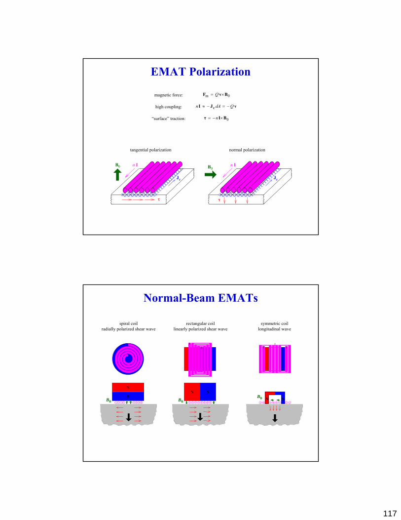
117
EMAT Polarization
en dA Q≈ − = −I J vhigh coupling:
0n= − ×τ I B“surface” traction:
m 0Q= ×F v Bmagnetic force:
tangential polarization normal polarization
Je
B0 n I
τ τ
B0n I
Je
Normal-Beam EMATs
spiral coilradially polarized shear wave
rectangular coillinearly polarized shear wave
symmetric coillongitudinal wave
B0S
N
N SB0
SN
B0

118
Angle-Beam Shear EMATs
sin λθ =
Λ
periodic permanent magnethorizontally polarized shear wave
SN
Λ
θ
B0
meander coilvertically polarized shear wave
S
N
θ
Λ
B0
EMAT Electronics
EMATs withpermanent or
electromagnets
driveramplifieroscillator
+_
Vsmatchingnetwork
matchingnetwork
specimen
0 0.5 1 1.5 2 2.5 3Frequency [MHz]
02468
101214161820
Impe
danc
e [Ω
]
resistancereactance
7-turn, 10-mm-diameter spiral coil on ferritic steel

119
Impedance Matching
VgV
gZ
Z≈
( )2
g *max g g g
gwhen ,
8V
P Z Z R R X XR
= = = = −
transformer (κ ≈ 1)
12 2122 11
Φ Φ= = κ
Φ Φ
2 2 21 22( )dV Ndt
= Φ + Φ
1 1 11 12( )dV Ndt
= Φ + Φ
I1
N1 N2 V2
Φ11
V1
I2
Φ22Φ12 Φ21,
2 21 1
V NV N
=
2 2 11 22( )dV Ndt
= Φ + Φ
1 1 11 22( )dV Ndt
= Φ + Φ2 11 2
I NI N
=2
2 221 1
NZZ N
=
ideal transformer (κ = 1)
7.3 EMAT Applications

120
Texture Assessment by EMATscold-pressed 2024 aluminum, 1.4 MHz, EMAT
η ≈ 0% (annealed) η = 0.45 % η = 0.8 % η = 1.6 %
cavg = 2,850 m/s, 0.2% per division, η = (cmax – cmin)/cavg
Textured Specimen
transmitter receiver
Rayleighwave
High-Temperature Monitoring
60
55
50
45
40
35
30
25
20200 400 600 800 1000
Temperature [K]
Stiff
ness
[G
Pa]
C44
C66
230
210
190
170
150
130200 400 600 800 1000
Temperature [K]
Stiff
ness
[G
Pa]
C11
C33
SiC/Ti-6Al-4V composite
(Ogi et al., 2001)

121
Electromagnetic Acoustic Resonance(Hirao and Ogi et al., 2003)
0 50 100 150
SCM 440 steel pure titanium
-120 -80 -40 0Stress [MPa]
-1.0
-1.1
-1.2
Bire
fring
ence
[%
]
loadunload
couplantPZT
specimen specimen
EMAT
Stress [MPa]
0.05
0
-0.05
-0.10
Bire
fring
ence
[%
]
as-receivedquenched & temperedannealed
Thank You!


![Fatigue Flaw NDE Reference Standard Development - Phase … · ultrasonic testing (UT), ... (EMAT), phased array ultrasound, and long-range guided wave (LRGW)]; electromagnetic methods](https://img.dokumen.tips/doc/110x75/5ac244ba7f8b9ae45b8e57f7/fatigue-flaw-nde-reference-standard-development-phase-testing-ut-emat.jpg)