Embed Size (px)
Citation preview

EEC 134 Project Report
RF/Microwave System Design
Fall - Winter 2016
Professor Liu
Team RF Eater
Qun Xia
Yueming Qiu
Tianyi Gao
Jiaming She

Abstract
This two quarters we work on a Frequency Modulated Continuous Wave (FMCW) radar
system, which can detect wide range of distant of an object. In this report, we will take about the
designing procedures and details.
Introduction
FMCW radar can be used to locate and detect objects, while Doppler radars can help to
determine the speed of an object. We mainly focused on the FMCW radar in our senior design
project. Our radar system include one transmitting antenna and one receiving antenna. Let the
transmitting antenna send out a signal. The signal will reach the object and be reflected back.
The receiving antenna will receive the signal that is reflected back. Then we can use laptop to
analyze the signal received in order to detect the distance between the radar and the object.
Designing Procedure
In fall quarter, we learned the knowledge needed for radar system design. Through each
instructed lab, we got a general idea of the function and characteristic of each RF component.
We also got familiar with PCB designing in fall quarter. Based on the experience from fall
quarter, we made the improvement plan at the beginning in winter quarter. Since all of our group
member have no background with embedding system, we decided to use laptop to do the
real-time signal processing but focus more on the accuracy of the measurement. In fall quarter,
unfortunately, the PCB our team designed and assembled in were all failed, so we decided to
focus more on improving the PCB from fall quarter instead of designing more new PCBs. We
divided the baseband circuit into three smaller PCB instead of a large one, which made the
debugging easier. We totally designed four PCBs for our radar system, one for each of the

following: function generator, voltage regulator and reference, active low-pass filter with gain
stage and low-noise amplifier. We also took off the attenuator. We planned to keep using metal
box for other RF components except the low-noise amplifier, which we believed will be more
stable and safe. Based on our plan, we made the quarter 2 schedule as shown in Fig 1.
● Timeline with Gantt Chart
Fig 1. Timeline
● Calculations
In fall quarter, we measured the gain of our can antenna and it is 7.348dB. Based on this
value and the following equation, we calculated the propagation loss for our system.

Distance Propagation loss
50m 96.2dB
25m 84.13dB
5m 56.17dB
1m 28.21dB Table 1. Propagation Loss
● Block Diagram for our Radar System
We made the block diagram for our final radar system according to the calculations.

Fig 2. Block Diagram for the Radar System
● PCB Design, Assembling and Testing
We totally designed four PCBs for our radar system, one for each of the following:
function generator, voltage regulator and reference, active low-pass filter with gain stage and
low-noise filter. When assembling the PCBs, we used the equipment from EFL lab in Bainer
Hall. Compared with the warm plate we used for heating our PCBs in fall quarter, the flow oven
in the EFL lab is more efficient and easy to use. We figured out that the PCBs from fall quarter
were all failed could be caused by that the heated temperature for the PCBs were not high
enough.
1. Voltage regulator and Reference
The first PCB we designed was the voltage regulator and reference. This PCB contained
two major components, LM317 and LT1009. LM317 worked as a voltage regulator. LT1009
with a 3.6K ohm resistor will work as precision voltage reference. The PCB is supposed to have
one output for 5V and one output for 2.5V when having a 8V power input.

Fig 6. Schematic for Voltage Regulator and Reference
Fig 6. PCB Layout for Voltage regulator and reference

Fig 7. Assembled Voltage Regulator and Reference PCB
In order to test the PCB, we connected the input of the PCB to a 8V power supply. Then
we used the multimeter to measure the voltage at the output for 5V. We adjust the potentiometer
until we got 5V. Then we measured voltage at the reference output pin. The voltage was 2.49V,
which suggested that the PCB for voltage regulator and reference PCB worked well. Then we
will use this PCB combined with the bench power supply working as a power supply for the rest
of the PCBs and circuits.
2. Function Generator
The second PCB we designed was the function generator, which include two major
components, teensy 3.1 and MCP4921. Teensy 3.1 is a microcontroller that will generate a
triangle wave and a square wave. MCP4921 is a Digital-to-Analog Converter (DAC) that can
convert the voltage value from teensy into frequency value that will go into voltage controlled
oscillator (VCO) later.

Fig 3. Schematic for function generator
Fig 4. PCB Layout for function generator

Fig 5. Assembled Function Generator
The function generator should generate a triangle wave with a 0.5-4.5V input range and
40ms period. We modified the code for teensy given in fall quarter to achieve the values we
want:
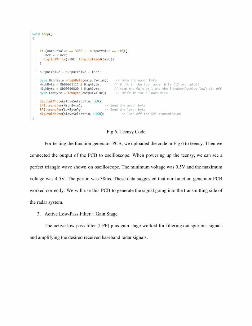
Fig 6. Teensy Code
For testing the function generator PCB, we uploaded the code in Fig 6 to teensy. Then we
connected the output of the PCB to oscilloscope. When powering up the teensy, we can see a
perfect triangle wave shown on oscilloscope. The minimum voltage was 0.5V and the maximum
voltage was 4.5V. The period was 38ms. These data suggested that our function generator PCB
worked correctly. We will use this PCB to generate the signal going into the transmitting side of
the radar system.
3. Active Low-Pass Filter + Gain Stage
The active low-pass filter (LPF) plus gain stage worked for filtering out spurious signals
and amplifying the desired received baseband radar signals.

Fig 7. Schematic for LPF + Gain Stage
Fig 8. PCB Layout for LPF + Gain Stage

Fig 9. Assembled LPF + Gain Stage PCB
In order to test the LPF + Gain Stage PCB, we connected the 5V and 2.5V power input
pins with the voltage regulator and reference PCB. Then we used the function generator in the
lab room to generate a 100 mVpp and 1k Hz signal and connect it to the input of the gain stage.
We used the oscilloscope to show the output signal of the filter. By adjusting the potentiometer,
we set the output peak to peak voltage of the PCB to be 3V and got the perfect sinusoidal wave
as shown in Figure 10. This plot suggested that our PCB worked properly.

Fig 10. Output Signal of LPF + Gain Stage PCB
4. Low-Noise Amplifier (LNA)
For the RF components in our system, we only designed a PCB for the low-noise
amplifier. We planned to use one LNA in the transmitting circuit and two LNAs in the receiving
circuit. Compared the radar system from fall quarter, we added one more LNA in the receiving
circuit. We believed that adding one more LNA could help with getting stronger signal for
analyzing. Thus, we assembled three LNA PCBs in our radar system.
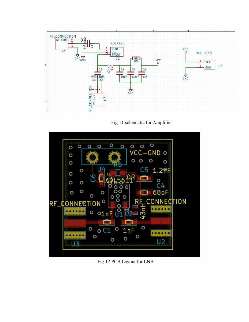
Fig 11 schematic for Amplifier
Fig 12 PCB Layout for LNA

Fig 13 Assembled LNA PCB
In order to test the LNA PCBs, we performed the lab 2 from fall quarter again by
replacing the metal box circuit with PCB. According to our measurement, the gain of all three
PCBs are 12 dB, 19.2 dB and 12.2 dB respectively. The current going into the PCB was about
1.2A. However, the lab 2 manual from fall quarter said it was supposed to be 0.5A. We first
thought they all worked properly. However, in our future testing with whole radar system, we
found out that the LNA generated too much signal instead of generated just one. Thus, we gave
up using the PCBs we designed and used metal box circuits for our final design.
● Antenna
Considering the weight, size and the stability of the whole system, we decided not to use
coffee cans for both transmitting and receiving antennas from last quarter. We finally decided to
use can antenna only for the transmitting antenna because the gain for can antenna is bigger than
the patch antenna. Since patch antenna are more light and steady, we decided to use patch

antenna as the receiving antenna. By considering the operating situation we need, we purchased
the Yagi Antenna online as our patch antenna. The Yagi antenna is able to operate at 2.4GHz.
Due to the measurement with the spectrum analyzer, we calculated out the patch antenna
gain to be :
-29.5dBm = 0.00117 mW
G = (4π* 1/ 0.125) * √(0.00117 / 1) = 3.439 = 5.364dBi
With the help from the TA, we performed the coupling tests for the two antennas and decided
that the distance between two antennas should be 10 inches.
Fig 14 Coupling test
According to the test for return loss (S11), the patch antenna and can antenna were
working with reasonable frequency. The bandwidth for the patch antenna is 0.6GHz, and the
bandwidth for the can antenna is 0.45GHz.

Fig 15. S11 result for patch antenna
Fig 16. S11 result for can antenna
● Testing
During this quarter, we have made several testings. In general, there were three testing
phases for our project. Through all the testing procedures, we have modified our radar system for
several times. We also modified some major components and tried several different forms of the
components. We finalized our radar system in Phase 3.

1. Phase 1
Before we got our PCB back, we started the first testing phase with breadboard circuits
and metal box RF components. In the first phase of testing, we built a radar system that is similar
to the one we built in fall quarter. We modified the system a little bit. We rearranged the circuit
for baseband on one breadboard. We tried our best to keep the legs for resistors and capacitors
shorter and made each part of the circuit close enough to each other. The baseband circuit
became simpler and clearer. This also helped decrease the power loss in the circuit and make the
circuit more accurate. We also took off the attenuator and added one more LNA at the receiving
end. We replaced both can antennas with two patch antennas.
Fig 17. Phase 1 Radar System

We used the software Audacity in the computer in our lab room to test the whole system
as instructed in lab 6 from fall quarter. Then we used the python code given in fall quarter to
analyzed the audio data we collected.
Fig 18. Phase 1 test result
Fig 18 shows the plot generated by the python code. The plot was not clear enough to tell
the position of the objects. Since there were so many objects in the lab room, too much
reflections from those objects could be a possible reason that resulted the plot we got. It was also
possible that the signal that received by the receiving antenna was too weak. We made
modifications and improvements to our radar system in the second testing phase.
2. Phase 2
When we received our PCBs, we started built the radar system with our PCBs. We
replaced all the three LNAs with PCBs, but then a problem happend with the circuit. When we
turned on the power supply, the power supply showed that there was overload happening in the
circuit. But when we disconnected the LNAs from the circuit, there were no overloading
happening. We thought the LNA PCBs may have too much gain.

Fig 19. Phase 2 system with LNAs in PCB
Then we modified the system and replaced two of the LNAs with metal box circuits. The
overloading problem was solved. We also replaced the transmitting antenna with can antenna,
because we found out that the can antenna has more gain than the patch antenna due to our
measurement. We performed test again. We first tested inside the lab room and got the following
result.
Fig 20. In-room test audio file

Fig 21. Phase 2 system in-room test result
However, we found out that the resulting plot generated by the python code was still not
too clear. By taking a detailed look with the audio file, we discovered that the audio plot was
constant, which suggested that the radar system did not work properly. Suggested by TA and
Professor Liu, we decided to check the transmitting side and receiving side of our system
separately. We tested our PCBs again but found no problems. Then we performed the labs from
last quarter again to test each RF components but found no problems. Finally we decided to ask
one of the TAs, Daniel, for help. With the help from Daniel, we found out that there was some
problem with the PCBs we designed for low-noise amplifier. The LNA took in too much signal
instead only one desired signal. Thus, we had to use the metal box circuits for all the LNAs in
our radar system. This became the final version of our system.
3. Phase 3
In the third phase of testing, we finalized our radar system.

Fig 22. Final Radar System
We first tested the system in the lab room. We got a very clear plot this time. As shown
in the following plot, we could see a clear path shown one of our group member walking away
from the radar and then walked back.
Fig 23. Final Radar System In-room Testing Result

In the final test competition, we used this final radar system and got the following results for
each test.
Fig 24. Final Test 1
Fig 25. Final Test 2

Fig 26. Final Test 3
Fig 27. Final Test 4

Fig 28. Final Test 5
As shown in the all five figures above, our radar system can detect the metal plate as far as 50
meters. From all those five figures, we can clearly know that TA were walking from nearly 50m
toward to us. The results we got are showing in the below figure.
Fig 29. Final Test Guessing Results

Bill of material
Components Price
1 × 8-DIP MCP4921 DAC IC $2.54
1 × LT1009 precision reference IC $1.05
1 × 14-DIP TL974IN quad Op-Amp IC $0.98
1 × Mini-Circuits ZX60-272LN-S+ RF amplifier
$39.95
2 x PCB Free
2 x PCB $30 each
2 x Antenna $5.99 each
TOTAL $116.5 Weight
The weight of our whole radar system is about 800 g. Conclusions
We have made a rough comparison between the final test guessing results and the real
results recorded by the TA. For first three tests, which were further, the errors were all about 10
meters. However, for the last two tests, which were close, the errors were much smaller.
The results suggested that our radar system worked but have large errors when measuring
objects from further distance. The possible reason could be caused by big power loss for signal
traveling in long distance. There is still a large space to improve our system.
During the two quarters, we have learned a lot about radar system design according to
this senior design projects. It was a great experience taking this designing course. We all
believed that this experience will be very helpful for our career in the future.
Appendix

● Datasheet
a) VCO: ZX95-2536C+
b) Power splitter ZX10-2-42+
c) Mixer ZX05-43LH-S+ :

Python code for analyzing the results:
# -*- coding: utf-8 -*- #range radar, reading files from a WAV file # Originially modified by Meng Wei, a summer exchange student (UCD GREAT Program, 2014) from Zhejiang University, China, from Greg Charvat's matlab code # Nov. 17th, 2015, modified by Xiaoguang "Leo" Liu, [email protected] import wave import os from struct import unpack import numpy as np from numpy.fft import ifft import matplotlib.pyplot as plt from math import log #constants c= 3E8 #(m/s) speed of light Tp = 20E-3 #(s) pulse duration T/2, single frequency sweep period. fstart = 2315E6 #(Hz) LFM start frequency

fstop = 2536E6 #(Hz) LFM stop frequency BW = fstop-fstart #(Hz) transmit bandwidth trnc_time = 0 #number of seconds to discard at the begining of the wav file window = False #whether to apply a Hammng window. # for debugging purposes # log file #logfile = 'log_new.txt' #logfh = open(logfile,'w') #logfh.write('start \n') #read the raw data .wave file here #get path to the .wav file #filename = os.getcwd() + '\\running_outside_20ms.wav' filename = os.getcwd() + '\\mar23-7.wav' # The initial 1/6 of the above wav file. To save time in developing the code #open .wav file wavefile = wave.open(filename, "rb") # number of channels nchannels = wavefile.getnchannels() # number of bits per sample sample_width = wavefile.getsampwidth() # sampling rate Fs = wavefile.getframerate() trnc_smp = int(trnc_time*Fs) # number of samples to discard at the begining of the wav file # number of samples per pulse N = int(Tp*Fs) # number of samples per pulse # number of frames (total samples) numframes = wavefile.getnframes() # trig stores the sampled SYNC signal in the .wav file #trig = np.zeros([rows,N]) trig = np.zeros([numframes - trnc_smp]) # s stores the sampled radar return signal in the .wav file #s = np.zeros([rows,N]) s = np.zeros([numframes - trnc_smp])

# v stores ifft(s) #v = np.zeros([rows,N]) v = np.zeros([numframes - trnc_smp]) #read data from wav file data = wavefile.readframes(numframes) for j in range(trnc_smp,numframes): # get the left (SYNC) channel left = data[4*j:4*j+2] # get the right (Data) channel right = data[4*j+2:4*j+4] #.wav file store the sound level information in signed 16-bit integers stored in little-endian format #The "struct" module provides functions to convert such information to python native formats, in this case, integers. if len(left) == 2: l = unpack('h', left)[0] if len(right) == 2:
r = unpack('h', right)[0] #normalize the value to 1 and store them in a two dimensional array "s" trig[j-trnc_smp] = l/32768.0 s[j-trnc_smp] = r/32768.0 #trigger at the rising edge of the SYNC signal trig[trig < 0] = 0; trig[trig > 0] = 1; #2D array for coherent processing s2 = np.zeros([int(len(s)/N),N]) rows = 0; for j in range(10, len(trig)): if trig[j] == 1 and np.mean(trig[j-10:j]) == 0: if j+N <= len(trig): s2[rows,:] = s[j:j+N] rows += 1 s2 = s2[0:rows,:] #pulse-to-pulse averaging to eliminate system performance drift overtime

for i in range(N): s2[:,i] = s2[:,i] - np.mean(s2[:,i]) #2pulse cancelation s3 = s2 for i in range(0, rows-1): s3[i,:] = s2[i+1,:] - s2[i,:] rows = rows-1 s3 = s3[0:rows,:] #apply a Hamming window to reduce fft sidelobes if window=True if window == True: for i in range(rows): s3[i]=np.multiply(s3[i],np.hamming(N)) ##################################### # Range-Time-Intensity (RTI) plot # inverse FFT. By default the ifft operates on the row v = ifft(s3) #get magnitude v = 20*np.log10(np.absolute(v)+1e-12) #only the first half in each row contains unique information v = v[:,0:int(N/2)] #normalized with respect to its maximum value so that maximum is 0dB m=np.max(v) grid = v grid=[[x-m for x in y] for y in v] # maximum range max_range =c*Fs*Tp/8/BW # maximum time max_time = Tp*rows plt.figure(0) plt.imshow(grid, extent=[0,max_range,0,max_time],aspect='auto', cmap =plt.get_cmap('gray')) plt.colorbar() plt.clim(0,-100) plt.xlabel('Range[m]',{'fontsize':20})

plt.ylabel('time [s]',{'fontsize':20}) plt.title('RTI with 2-pulse clutter rejection',{'fontsize':20}) plt.tight_layout() plt.show() #plt.subplot(612) #plt.plot(grid[5]) #plt.subplot(613) #plt.plot(grid[6]) #plt.subplot(614) #plt.plot(grid[20]) # #plt.subplot(615) #plt.plot(grid[30]) #plt.subplot(616) #plt.plot(grid[40])


![Xiaoguang ``Leo'' Liu – liuxiaoguang Department of ...dart.ece.ucdavis.edu/people/files/CV_Xiaoguang_Liu.pdf · [J14] Akash Anand and Xiaoguang Liu, “Reconfigurable Planar Capacitive](https://img.dokumen.tips/doc/110x75/5f30ef34e680897ca810e5d6/xiaoguang-leo-liu-a-liuxiaoguang-department-of-dartece-j14-akash-anand.jpg)


