Embed Size (px)
Citation preview

JOURNAL OF MICROELECTROMECHANICAL SYSTEMS, VOL. XX, NO. XX, FEBRUARY 2010 1
High-Q Tunable Microwave Cavity Resonators andFilters using SOI-based RF MEMS Tuners
Xiaoguang Liu, Student Member, IEEE, Linda P. B. Katehi, Fellow, IEEE, William J. Chappell, Member, IEEEand Dimitrios Peroulis, Member, IEEE
Abstract—This paper presents the modeling, design, fabri-cation and measurement of MEMS-enabled continuously tun-able evanescent-mode electromagnetic cavity resonators and fil-ters with very high unloaded quality factors (Qu). Integratedelectrostatically-actuated thin diaphragms are used for the firsttime for tuning the frequency of the resonators/filters. Anexample tunable resonator with 2.6:1 (5.0 − 1.9 GHz) tuningratio, Qu of 300 − 650 is presented. A continuously tunable 2-pole filter from 3.04 GHz to 4.71 GHz with 0.7% bandwidth andinsertion loss of 3.55 − 2.38 dB is also shown as a technologydemonstrator. Mechanical stability measurements show that thetunable resonators/filters exhibit very low frequency drift (lessthan 0.5% for 3 hours) under constant bias voltage. Thispaper significantly expands upon previously reported tunableresonators [1].
Index Terms—Evanescent-mode cavity, MEMS, quality factor,tuning, tunable filter, tunable resonator, electrostatic actuation
I. INTRODUCTION
TUNABLE RF/Microwave filters are essential componentsfor the next generation reconfigurable radio front-ends in
wireless communication systems with multi-band and multi-standard characteristics [2]. Several technologies exist formaking tunable RF/Microwave filters. Yttrium-Iron-Garnet(YIG) resonator based tunable filters are the most widelyused and exhibit a very wide tuning range over multipleoctaves and a very high unloaded quality factor Qu (10, 000at 10 GHz) [3]. Nevertheless, the large volume (approximately1 in3) and high power consumption (0.75−3 W) of YIG basedtunable filters hinder their integration into mobile communi-cation systems. Alternative approaches have been proposedto make miniaturized tunable RF/Microwave filters. Theseapproaches are based on micromechanical resonators [4]–[6], cavity filters [7], [8], planar transmission line resonatorsloaded with solid-state varactors [9], ferroelectric-tuned varac-tors [10]–[12] and MEMS varactors/switches [13]–[15]. Thesetechnologies have achieved either a) very high Qu at the costof limited tuning range (< 2%), such as micro-mechanical
X. Liu, W. J. Chappell and D. Peroulis are with the School of Electrical andComputer Engineering, Purdue University, West Lafayette, IN, 47906 USAe-mail: [email protected], [email protected] and [email protected].
L. P. B. Katehi is with the University of California, Davis, CA, USA. email:[email protected].
This work has been supported by the Defense Advanced Research ProjectsAgency under the ASP Program with a subcontract from BAE Systems.The views, opinions, and/or findings contained in this article/presentation arethose of the author/presenter and should not be interpreted as representingthe official views or policies, either expressed or implied, of the DefenseAdvanced Research Projects Agency or the Department of Defense.
The authors are grateful to Hjalti H. Sigmarsson and Himanshu Joshi ofPurdue University for helpful discussions and technical assistance.
filters [6]; or b) high tuning range at the cost of low Qu (< 200@ 5 GHz), such as MEMS varactor tuned filters.
Recently, however, there has been some success in realizingwidely tunable filters with simultaneous high-Qu and lowinsertion loss using evanescent-mode cavity resonators withMEMS tuners [1], [16]–[18]. In [16], Hou et al. presentedpreliminary results on tunable micromachined evanescent-mode resonator with Qu of 200 at 2.5 GHz and 120 at 4GHz. Joshi et al. demonstrated substrate integrated evanescent-mode tunable filters with high tuning range (2.3 − 4 GHz)and high Qu (360 − 700) [17]. Both designs use an externalpiezoelectric actuator as the tuning element. The well-knownhysteresis and creep of piezoelectric actuators present signif-icant system level problems for these tunable resonators andfilters (see Section III for detailed discussion). In [18], Park etal. demonstrated a 2-pole evanescent-mode filter using MEMSvaractor networks. The achieved tuning range and Qu waslimited to 4.3 − 5.5 GHz and 273 − 511 respectively. In [1],the authors of this paper demonstrated a tunable resonator withQu of 460− 530 in the 3.4− 6.2 GHz range. An electrostaticthin diaphragm MEMS tuner was used for its high precision,high reliability and near zero hysteresis.
In this paper, we build on our previous work and investigatethe use of electrostatically-actuated evanescent-mode cavityresonators for making tunable RF/Microwave filters with si-multaneous wide tuning range and high Qu. Specifically, inrelation to [1], we present the optimized results of tunableresonators with state-of-the-art performance in terms of tuningrange (1.9 − 5.0 GHz, i.e. 2.6:1 ratio), Qu (300 − 650) andstability. The modeling methodology and design trade-offs ofelectrostatically-actuated MEMS tuner are discussed in detailwith focus on the interdependences of tuning range, actuationvoltage, tuning speed and long term stability. The design,fabrication and characterization of a 3.04 − 4.71 GHz two-pole tunable bandpass filter with insertion loss of 3.55− 2.38dB is presented as a demonstrator for this technology.
The organization of this paper is as follows. In Section II,the fundamental concepts and design methods of evanescent-mode cavity resonators are reviewed and presented. Section IIIdiscusses the various design considerations and trade-offs forthe electrostatic thin diaphragm MEMS tuner. Section IVpresents the fabrication and assembly techniques for makingthe proposed tunable resonators/filters. Measurement and dis-cussions of the fabricated tunable resonator are presented inSection V. In Section VI, the design and measurements of a2-pole tunable bandpass filter are presented.
JOURNAL OF MICROELECTROMECHANICAL SYSTEMS, VOL. XX, NO. XX, FEBRUARY 2010 2
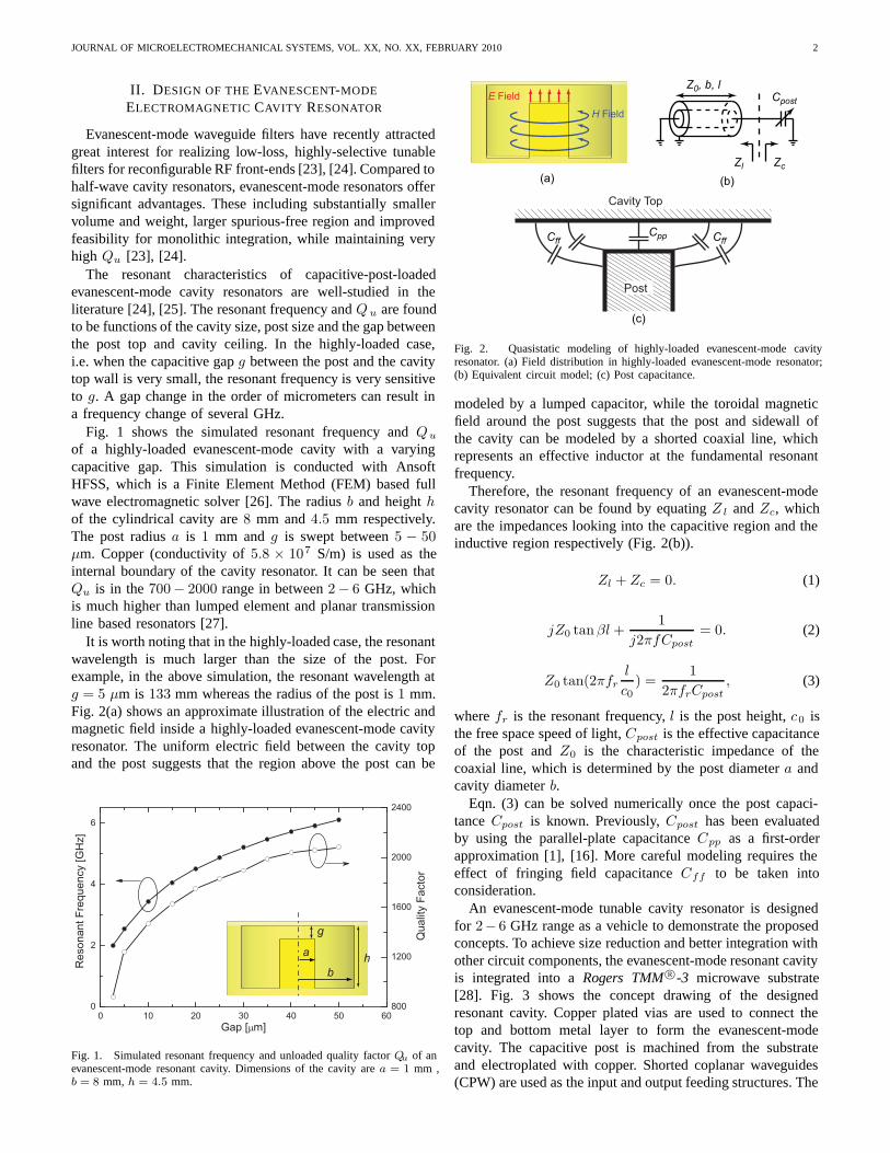
II. DESIGN OF THE EVANESCENT-MODE
ELECTROMAGNETIC CAVITY RESONATOR
Evanescent-mode waveguide filters have recently attractedgreat interest for realizing low-loss, highly-selective tunablefilters for reconfigurable RF front-ends [23], [24]. Compared tohalf-wave cavity resonators, evanescent-mode resonators offersignificant advantages. These including substantially smallervolume and weight, larger spurious-free region and improvedfeasibility for monolithic integration, while maintaining veryhigh Qu [23], [24].
The resonant characteristics of capacitive-post-loadedevanescent-mode cavity resonators are well-studied in theliterature [24], [25]. The resonant frequency and Q u are foundto be functions of the cavity size, post size and the gap betweenthe post top and cavity ceiling. In the highly-loaded case,i.e. when the capacitive gap g between the post and the cavitytop wall is very small, the resonant frequency is very sensitiveto g. A gap change in the order of micrometers can result ina frequency change of several GHz.
Fig. 1 shows the simulated resonant frequency and Qu
of a highly-loaded evanescent-mode cavity with a varyingcapacitive gap. This simulation is conducted with AnsoftHFSS, which is a Finite Element Method (FEM) based fullwave electromagnetic solver [26]. The radius b and height hof the cylindrical cavity are 8 mm and 4.5 mm respectively.The post radius a is 1 mm and g is swept between 5 − 50μm. Copper (conductivity of 5.8 × 10⁷ S/m) is used as theinternal boundary of the cavity resonator. It can be seen thatQu is in the 700− 2000 range in between 2 − 6 GHz, whichis much higher than lumped element and planar transmissionline based resonators [27].
It is worth noting that in the highly-loaded case, the resonantwavelength is much larger than the size of the post. Forexample, in the above simulation, the resonant wavelength atg = 5 μm is 133 mm whereas the radius of the post is 1 mm.Fig. 2(a) shows an approximate illustration of the electric andmagnetic field inside a highly-loaded evanescent-mode cavityresonator. The uniform electric field between the cavity topand the post suggests that the region above the post can be
h
g
a
b
Fig. 1. Simulated resonant frequency and unloaded quality factor Qu of anevanescent-mode resonant cavity. Dimensions of the cavity are a = 1 mm ,b = 8 mm, h = 4.5 mm.
(a)
Z0, b, l
Zl Zc
Cpost
(b)
Post
Cavity Top
(c)
Cpp CffCff
E Field
H Field
Fig. 2. Quasistatic modeling of highly-loaded evanescent-mode cavityresonator. (a) Field distribution in highly-loaded evanescent-mode resonator;(b) Equivalent circuit model; (c) Post capacitance.
modeled by a lumped capacitor, while the toroidal magneticfield around the post suggests that the post and sidewall ofthe cavity can be modeled by a shorted coaxial line, whichrepresents an effective inductor at the fundamental resonantfrequency.
Therefore, the resonant frequency of an evanescent-modecavity resonator can be found by equating Z l and Zc, whichare the impedances looking into the capacitive region and theinductive region respectively (Fig. 2(b)).
Zl + Zc = 0. (1)
jZ0 tan βl +1
j2πfCpost= 0. (2)
Z0 tan(2πfrl
c0) =
12πfrCpost
, (3)
where fr is the resonant frequency, l is the post height, c0 isthe free space speed of light, Cpost is the effective capacitanceof the post and Z0 is the characteristic impedance of thecoaxial line, which is determined by the post diameter a andcavity diameter b.
Eqn. (3) can be solved numerically once the post capaci-tance Cpost is known. Previously, Cpost has been evaluatedby using the parallel-plate capacitance Cpp as a first-orderapproximation [1], [16]. More careful modeling requires theeffect of fringing field capacitance Cff to be taken intoconsideration.
An evanescent-mode tunable cavity resonator is designedfor 2− 6 GHz range as a vehicle to demonstrate the proposedconcepts. To achieve size reduction and better integration withother circuit components, the evanescent-mode resonant cavityis integrated into a Rogers TMM R©-3 microwave substrate[28]. Fig. 3 shows the concept drawing of the designedresonant cavity. Copper plated vias are used to connect thetop and bottom metal layer to form the evanescent-modecavity. The capacitive post is machined from the substrateand electroplated with copper. Shorted coplanar waveguides(CPW) are used as the input and output feeding structures. The

JOURNAL OF MICROELECTROMECHANICAL SYSTEMS, VOL. XX, NO. XX, FEBRUARY 2010 3
Cavity formedby metalized vias
CapacitivePost
Output Port
30 mm
4.5 mm
2.5 mm
18 mm
(a)
(b)
Input Port6 mm
Fig. 3. Concept drawing of the evanescent-mode cavity in Rogers TMMR©-3substrate. The MEMS actuator, which is not shown in this drawing, is to bediscussed in Section III.
transverse magnetic field of the shorted CPW is coupled withthe toroidal magnetic field (Fig. 2(a)) around the capacitivepost to achieve input and output coupling. Dimensions of thecavity design are labeled in Fig. 3.
Fig. 4 shows the simulated resonant frequency and Qu ofthe designed tunable resonator. The thickness of the top wallof the cavity (not shown in Fig. 3) is assumed to be 0.5 μmin the simulation. It can be seen that the resonant frequencychanges from 2 GHz to 6 GHz when g0 changes from 2 μmto 17 μm. This leads to a simulated Qu change from 350 to1100. It is obvious that a deflection of ∼ 15 μm is needed toachieve a tuning ratio of 3 : 1, and ∼ 10 μm is needed for2 : 1. Such large deflections present challenges to the designof the MEMS tuner, which will be discussed in detail in thenext section.
Fig. 4. Simulated resonant frequency and Qu of designed tunable evanescent-mode cavity resonator. The MEMS actuator is assumed to have a maximumstroke of 15−20 µm. Dimensions of the design in this simulation are shownin Fig. 3.
III. DESIGN AND INTEGRATION OF MEMS DIAPHRAGM
TUNER
A. Actuation Scheme
Frequency tuning is achieved by deflecting a thin metallicdiaphragm which is placed on top of the evanescent-modecavity (Fig. 6). Several methods can be used for the actuationof the diaphragm, including electrothermal, piezoelectric andelectrostatic actuations. The high power consumption and lowspeed of electrothermal actuation makes it undesirable forportable applications. Piezoelectric actuation consumes littlepower and can generate high actuation force. Joshi et al.demonstrated piezo-actuated evanescent-mode tunable filterswith high Qu and a wide tuning range [17]. However, it iswell known that piezoelectric actuators have hysteresis andcreep problems [19]–[22]. As an example, a piezo-actuatorused in [17] is taken for deflection measurement using anOlympus LEXT R© microscope. The LEXT R© is a laser confocalmicroscope and has a measurement uncertainty of < 0.1 μm.Fig. 5 shows the deflection of the piezo-actuator with bias volt-age cycled between −210 V to 210 V. Hysteresis is observedover several cycles. With the hysteresis and creep behaviorsof the piezo-actuator, repeatable and reliable frequency tuningwith high precision can become a system level problem.
Voltage Up
Voltage Down
Fig. 5. Deflection measurement on a piezo-actuator used in [17] showssubstantial hysteresis.
Electrostatic actuation, on the other hand, can be precise,reliable and hysteresis-free. Therefore we choose to use elec-trostatic actuation in this work. Fig. 6 shows a concept drawingof the electrostatic diaphragm actuator. The diaphragm consistsof a layer of gold deposited on the released device layerof an silicon-on-insulator (SOI) wafer. Due to its stress-freeand defect-free nature, the single-crystal silicon device layerserves as a flexible yet robust mechanical support to the goldlayer. The Au-Si composite diaphragm is packaged on topof the capacitive post to form the tunable resonator. Whena bias voltage is applied to the actuation electrode placed adistance d0 above the diaphragm, electrostatic force will pullthe diaphragm away from the capacitive post to change theresonant frequency. An important advantage of using a planardiaphragm is that it does not distort the natural current flow

JOURNAL OF MICROELECTROMECHANICAL SYSTEMS, VOL. XX, NO. XX, FEBRUARY 2010 4
Bia Electrode
MEMS DiaphragmActuator
Capacitive Post
Metalized Vias
SOI Wafer
d0
g0
(b)
Bias Electrode
Thin DiaphragmActuator
(a)
Fig. 6. Concept drawing of the MEMS thin diaphragm tuner. (a) Theintegration of thin diaphragm tuner with the evanescent-mode resonant cavity;(b) A close-up view of the MEMS tuner.
and preserves the high Qu of the cavity resonator, leading tovery low filter insertion loss. This design is also inherentlyreliable and tolerant to material and process variations due tothe use of SOI-based fabrication process.
B. Electro-mechanical Considerations
Several parameters are of concern in the design of the elec-trostatic actuator, including tuning range, actuation voltage,tuning speed and long term stability.
1) Tuning RangeThe maximum deflection of the diaphragm directly
relates to the tuning ratio of the resonator. Indeed, thetuning ratio is roughly given by (4) [1]
Rmax ≈√
g0 + d0/3g0
. (4)
It can be seen that the tuning ratio can be increased bydecreasing the initial gap g0. However, excessively smallg0 can cause significant difficulty in the accuracy andyield of the tunable resonator. Qu is also compromisedwith a small g0. In this design, an initial gap g0 = 2 μmis used with consideration given for both high tuningrange and high Qu. In order to achieve a tuning ratio of> 2:1, a minimum d0 of 30 μm is required.
2) Actuation VoltageIt is generally desirable to keep the actuation voltage
as low as possible. In tunable filters with multiple res-onators, the resonant frequency of each resonator mustbe precisely aligned according to the specific design.Therefore analog tuning of the resonant frequency is
highly desirable. In the analog tuning region of anelectrostatic actuator, the maximum actuation voltagecan not exceed the pull-in voltage. The pull-in voltageVpi of the diaphragm tuner is given by (5), in which Wis the side length of the square bias electrode, d0 is theinitial actuation gap and k is the spring constant for thediaphragm [27].
Vpi =
√8kd3
0
27εW 2(5)
The spring constant of a circular diaphragm is givenby
k = k′ + k′′ =Et3
0.0138 w2+
π2σt
7.2(6)
where w and t are the diaphragm side length andthickness, E is the Young’s modulus, and σ is theresidual stress [29], [30]. As previously noted, the singlecrystal silicon device layer is a nearly stress free materialand the residual stress is mainly due to the thin Au layer.For thin diaphragms, the k ′′ term dominates the springconstant value in the presence of practical residual stress(> 5 MPa). For example, for a 3.5 μm thick diaphragm(0.5 μm Au on top of 3 μm single crystal silicon) witha size of 2 × 2 mm2, Au residual stress of 30 MPa anda d0 of 40 μm, the pull-in voltage is 415 V.
To lower the actuation voltage to an acceptable range,it is desirable to lower the spring constant k by reducingeither the residual stress or the thickness of the Aufilm. However, the reduction of residual stress in theAu film is limited by fabrication process tolerances andextremely low stress (< 5 MPa) is very difficult toachieve [27]. Reduction of the Au film thickness alsocomes with a penalty in higher RF loss. The Au skindepth at 2−6 GHz range is 1.76−1.02 μm. It is desirableto have a Au layer thickness larger than the skin depth atthis frequency range. Careful compromise must be madein choosing Au film thickness from the mechanical pointof view. Fig. 7 shows HFSS simulations of the Qu of anevanescent-mode resonator with different Au thicknesson the top wall. It can be seen that there is a significantdrop in Qu for Au thickness less than 0.5 μm at 2 − 6GHz.
Whereas a high spring constant k is limited by processtolerance and quality factor requirements, the size ofthe diaphragm can be increased to reduce the actuationvoltage. Although a larger diaphragm has relativelyinsignificant impact on k (diaphragm size only comesinto play in the k′ term, which is dominated by thek′′ term), it can accommodate a larger bias electrode,therefore reducing the required actuation voltage.
3) Long Term Mechanical StabilityLong term mechanical stability is an additional ben-
efit of using a larger diaphragm. The high Qu of theevanescent-mode tunable resonator makes it a promisingcandidate for use in very narrow band tunable filters. Forsuch filters, frequency precision and stability is a critical

JOURNAL OF MICROELECTROMECHANICAL SYSTEMS, VOL. XX, NO. XX, FEBRUARY 2010 5
Fig. 7. Simulated Qu with different Au thin film thickness. Cavitydimensions are the same as in Fig. 4
concern. In order to improve the frequency stabilityand compensate for any frequency misalignment dueto fabrication tolerances, a closed-loop control systemis needed to continuously monitor and adjust the biasvoltage to maintain a stable frequency response. In orderto ease the control loop design, the proposed tunableresonator needs to have a stable frequency response.
It is well known that material creep and viscoelas-ticity are important factors affecting the long termperformances of MEMS devices. Creep is defined asthe strain response of a material under constant stress.Viscoelasticity is referred to as the time dependentresponse to an applied force. It has been shown thatcreep/viscoelasticity leads to material property changeunder non-zero loading over time. These parameterchanges are often characterized as an effective Young’smodulus drift [31], [32].
In our tunable resonator design, the effective Young’smodulus drift will result in resonant frequency shiftover time. It has been shown that the effectiveYoung’s modulus drift rate is directly related to theinduced stress/strain in the actuating structure. Lowerstress/strain results in lower drift. Fig. 8 shows thesimulated induced stresses in square diaphragms ofdifferent sizes at varying deflections. Simulation is donewith the Coventorware MEMS simulation package [34].It is shown that larger diaphragms have inherently lowerstress for a given deflection. Apart from lower actuationvoltage, larger diaphragms also demonstrate lower fre-quency drift rates.
4) Tuning SpeedThe compromise of employing a relatively large
diaphragm lies in slower response time due to itslarger mass and smaller spring constant. For example,Fig. 9 shows the calculated actuation time for squarediaphragms of varying side lengths using a simple 1-Dspring-mass model [27]. The thicknesses of the Si andAu film are assumed to be 3 μm and 0.5 μm respectively.A residual stress of 30 MPa is used in the calculation
Induced Stress
Fig. 8. Simulated induced stress in actuated square diaphragms of differentsizes (side length).
Fig. 9. Calculated actuation speed of diaphragms of varying sizes.
and a mechanical Q of 0.1 is assumed. It can be seenfrom Fig. 9 that larger diaphragms take longer time toactuate. To improve the tuning speed, air vent holes canbe added to the diaphragm. In such a case, the air holesmay adversely affect the Qu of the resonator.
5) Temperature StabilityTemperature stability may be another concern for
the SOI-based diaphragm tuners. The use of differentmaterials with different coefficients of thermal expansion(CTE) in the fabrication process need to be consideredas well. As mentioned in Section III-B-3), however,a close-loop feedback control system can be used tocompensate for any frequency drift due to environmentalperturbations. This is in general necessary for high-Qtunable systems [35].
From the above discussion, it is clear that careful consid-eration and suitable compromises among the resonator’s actu-ation voltage, frequency tunability, quality factor, mechanicalrobustness/stability, resistance to creep and tuning speed need
JOURNAL OF MICROELECTROMECHANICAL SYSTEMS, VOL. XX, NO. XX, FEBRUARY 2010 6
(a)
(b)
(c)
(d)
AZ9260
Si Handle
Si
SiO2
Au
(e)
Fig. 10. Fabrication process for MEMS diaphragm: (a) AZ9260 patterning;(b) DRIE; (c) Oxide etch; (d) Au sputter; (e) Fabricated MEMS Diaphragmpiece.
to be made to satisfy the requirements of a given application.
IV. FABRICATION TECHNOLOGY
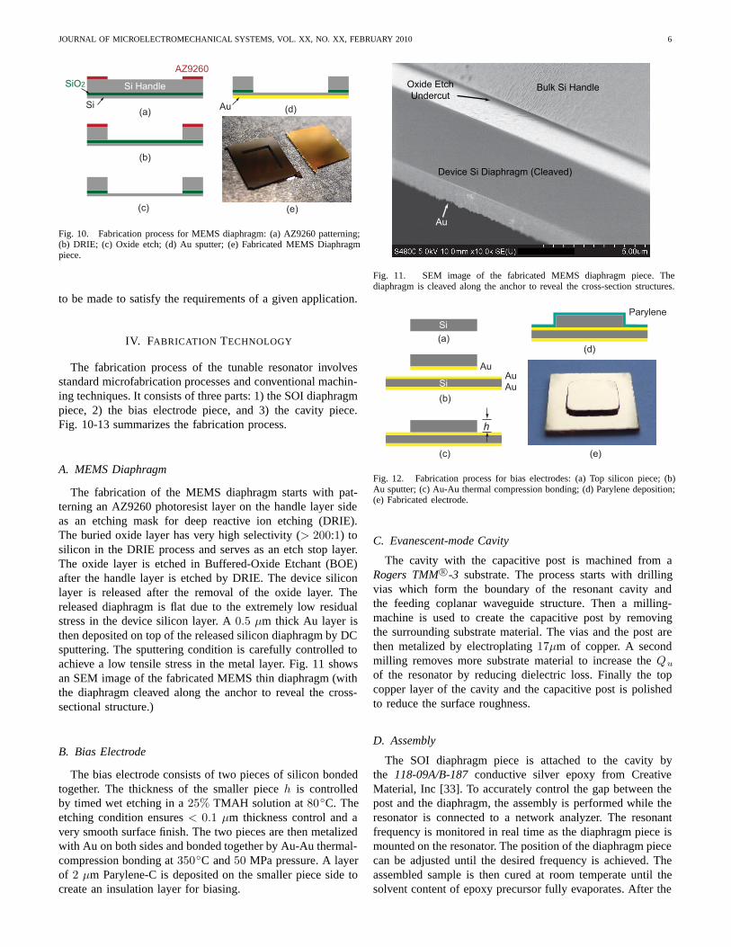
The fabrication process of the tunable resonator involvesstandard microfabrication processes and conventional machin-ing techniques. It consists of three parts: 1) the SOI diaphragmpiece, 2) the bias electrode piece, and 3) the cavity piece.Fig. 10-13 summarizes the fabrication process.
A. MEMS Diaphragm
The fabrication of the MEMS diaphragm starts with pat-terning an AZ9260 photoresist layer on the handle layer sideas an etching mask for deep reactive ion etching (DRIE).The buried oxide layer has very high selectivity (> 200:1) tosilicon in the DRIE process and serves as an etch stop layer.The oxide layer is etched in Buffered-Oxide Etchant (BOE)after the handle layer is etched by DRIE. The device siliconlayer is released after the removal of the oxide layer. Thereleased diaphragm is flat due to the extremely low residualstress in the device silicon layer. A 0.5 μm thick Au layer isthen deposited on top of the released silicon diaphragm by DCsputtering. The sputtering condition is carefully controlled toachieve a low tensile stress in the metal layer. Fig. 11 showsan SEM image of the fabricated MEMS thin diaphragm (withthe diaphragm cleaved along the anchor to reveal the cross-sectional structure.)
B. Bias Electrode
The bias electrode consists of two pieces of silicon bondedtogether. The thickness of the smaller piece h is controlledby timed wet etching in a 25% TMAH solution at 80◦C. Theetching condition ensures < 0.1 μm thickness control and avery smooth surface finish. The two pieces are then metalizedwith Au on both sides and bonded together by Au-Au thermal-compression bonding at 350◦C and 50 MPa pressure. A layerof 2 μm Parylene-C is deposited on the smaller piece side tocreate an insulation layer for biasing.
Device Si Diaphragm (Cleaved)
Bulk Si Handle
Au
Oxide EtchUndercut
Fig. 11. SEM image of the fabricated MEMS diaphragm piece. Thediaphragm is cleaved along the anchor to reveal the cross-section structures.
(a)
(b)
(c)
(d)
AuAu
Si
Si Au
Parylene
h
(e)
Fig. 12. Fabrication process for bias electrodes: (a) Top silicon piece; (b)Au sputter; (c) Au-Au thermal compression bonding; (d) Parylene deposition;(e) Fabricated electrode.
C. Evanescent-mode Cavity
The cavity with the capacitive post is machined from aRogers TMM R©-3 substrate. The process starts with drillingvias which form the boundary of the resonant cavity andthe feeding coplanar waveguide structure. Then a milling-machine is used to create the capacitive post by removingthe surrounding substrate material. The vias and the post arethen metalized by electroplating 17μm of copper. A secondmilling removes more substrate material to increase the Qu
of the resonator by reducing dielectric loss. Finally the topcopper layer of the cavity and the capacitive post is polishedto reduce the surface roughness.
D. Assembly
The SOI diaphragm piece is attached to the cavity bythe 118-09A/B-187 conductive silver epoxy from CreativeMaterial, Inc [33]. To accurately control the gap between thepost and the diaphragm, the assembly is performed while theresonator is connected to a network analyzer. The resonantfrequency is monitored in real time as the diaphragm piece ismounted on the resonator. The position of the diaphragm piececan be adjusted until the desired frequency is achieved. Theassembled sample is then cured at room temperate until thesolvent content of epoxy precursor fully evaporates. After the

JOURNAL OF MICROELECTROMECHANICAL SYSTEMS, VOL. XX, NO. XX, FEBRUARY 2010 7
(a)
(b)
(c)
(d)
(e)
Cu
TMM Substrate
Fig. 13. Fabrication process for evanescent-mode cavity: (a) TMMR©-3substrate with double side copper laminate; (b) Via and post milling; (c)Cu plating; (d) Cavity milling; (e) Fabricated cavity piece. The dashed linein (d) represent the boundary of the electromagnetic resonant cavity.
MEMS Diaphragm ActuatorSMA Connector
SMAConnector
Evanescent-modeResonant Cavity
Fig. 14. Fabricated evanescent-mode electromagnetic tunable cavity res-onator. The bias electrode in this figure is not permanently fixed to theresonator to reveal the thin diaphragm tuner.
assembly is completed, two SMA connectors are soldered toboth ends of the resonator to characterize the RF performance.
From a production stand point, it is desirable to haveaccurate and repeatable control over the gap. However, thecurrent technology using TMM R©-3 substrate is limited by thesurface roughness of the substrate and the copper laminate.A bonding process with a precise vertical alignment is beingdeveloped using Si micromachined evanescent-mode cavities.This holds great promise in achieving a low-cost reliableassembly for tunable resonators.
V. MEASUREMENTS AND DISCUSSION
A. Actuation Measurement
The deflection of the thin diaphragm under different biasvoltages is measured with an Olympus LEXT R© microscopethat has a measurement uncertainty of < 0.1 μm. Fig. 15(a)shows the measurement setup. The bias electrode is placed un-derneath the diaphragm tuner. Bias voltages ranging between0−130 V are applied to actuate the diaphragm. The deflectionof the center point of the diaphragm is recorded with the LEXTat each bias voltage.
Fig. 15(b) shows the measured deflection-voltage profile. Amaximum deflection of 14.3 μm is achieved before pull-in at
Dia
phra
gm D
efle
ctio
n [m
m]
Bias Electrode
Evanescent-mode Cavity
MEMSDiaphragm
V
Pull-in
(a)
(b)
Voltage Up
Voltage Down
Fig. 15. Deflection-voltage measurement of the MEMS thin diaphragm tuner.A maximum deflection of 14.3 µm is achieved.
122 V. The large range of diaphragm movement ensures a hightuning range for the tunable resonator. The extracted initialgap g0 and bias gap d0 are 1.8 ± 0.01 μm and 40 ± 2 μmrespectively. No hysteresis is observed in the analog tuningregion.
B. RF Measurements
The RF measurements of an assembled tunable resonatorare taken with an Agilent 8722ES vector network analyzer.The tuning response of the measured resonator is shown inFig. 16. The resonator is intentionally designed to be weaklycoupled for more accurate extraction of the resonant frequencyand Qu.
With less than 120 V bias voltage, the resonant frequencyof the tunable resonator can be tuned between 5.0− 1.9 GHz,achieving a tuning ratio of 2.6:1. Although only a selection ofmeasurements are shown in Fig. 16(a), the frequency tuning isfully analog with < 100 kHz precision. A 1-2 mV precision in
JOURNAL OF MICROELECTROMECHANICAL SYSTEMS, VOL. XX, NO. XX, FEBRUARY 2010 8
(a)
(b)
Fig. 16. Measured weakly-coupled transmission (a) and extracted Qu (b)of the fabricated tunable resonator.
the control of bias voltage is required to achieve this frequencyprecision.
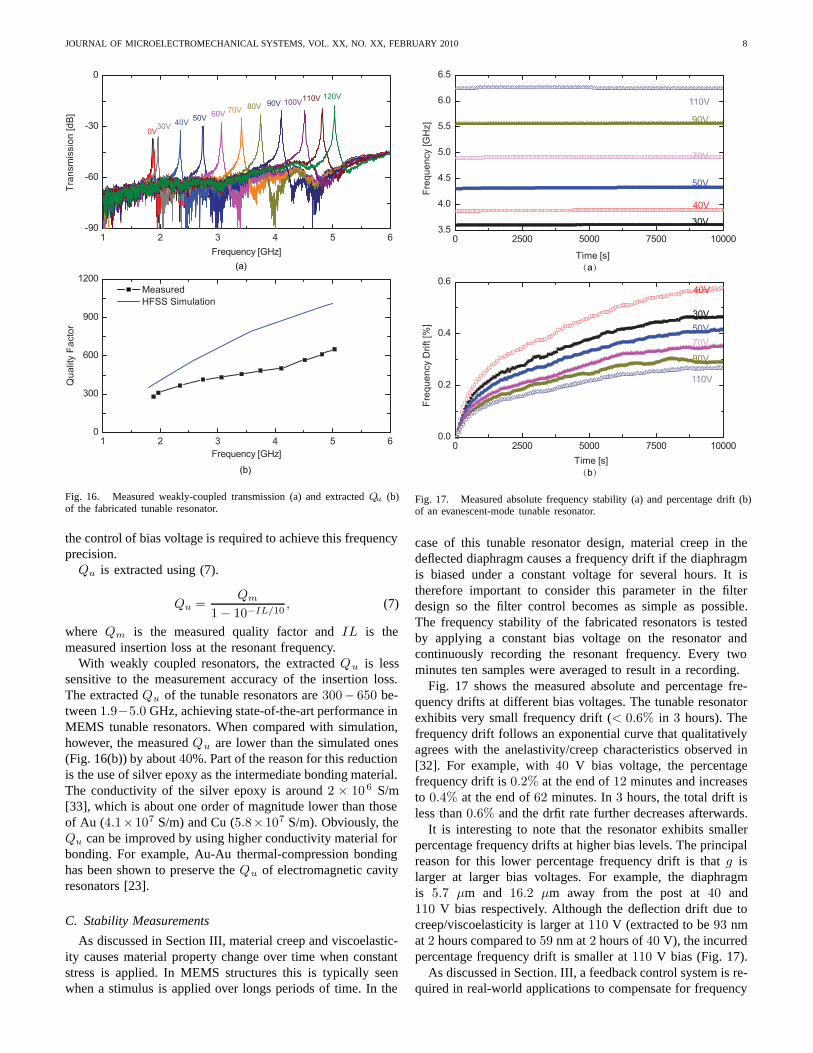
Qu is extracted using (7).
Qu =Qm
1 − 10−IL/10, (7)
where Qm is the measured quality factor and IL is themeasured insertion loss at the resonant frequency.
With weakly coupled resonators, the extracted Qu is lesssensitive to the measurement accuracy of the insertion loss.The extracted Qu of the tunable resonators are 300− 650 be-tween 1.9−5.0 GHz, achieving state-of-the-art performance inMEMS tunable resonators. When compared with simulation,however, the measured Qu are lower than the simulated ones(Fig. 16(b)) by about 40%. Part of the reason for this reductionis the use of silver epoxy as the intermediate bonding material.The conductivity of the silver epoxy is around 2 × 10 6 S/m[33], which is about one order of magnitude lower than thoseof Au (4.1×10⁷ S/m) and Cu (5.8×10⁷ S/m). Obviously, theQu can be improved by using higher conductivity material forbonding. For example, Au-Au thermal-compression bondinghas been shown to preserve the Qu of electromagnetic cavityresonators [23].
C. Stability Measurements
As discussed in Section III, material creep and viscoelastic-ity causes material property change over time when constantstress is applied. In MEMS structures this is typically seenwhen a stimulus is applied over longs periods of time. In the
30V
40V
50V70V70V
90V
110V110V
30V
40V
50V
70V70V
90V
110V110V
(a)
(b)
Fig. 17. Measured absolute frequency stability (a) and percentage drift (b)of an evanescent-mode tunable resonator.
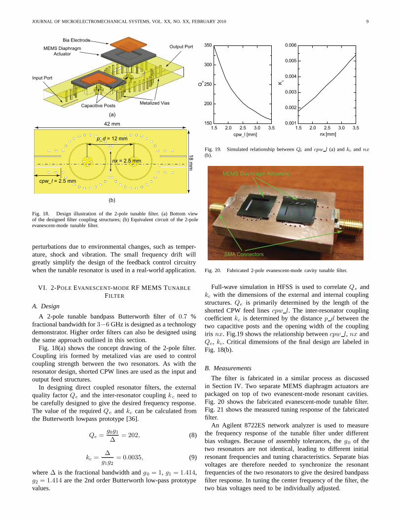
case of this tunable resonator design, material creep in thedeflected diaphragm causes a frequency drift if the diaphragmis biased under a constant voltage for several hours. It istherefore important to consider this parameter in the filterdesign so the filter control becomes as simple as possible.The frequency stability of the fabricated resonators is testedby applying a constant bias voltage on the resonator andcontinuously recording the resonant frequency. Every twominutes ten samples were averaged to result in a recording.
Fig. 17 shows the measured absolute and percentage fre-quency drifts at different bias voltages. The tunable resonatorexhibits very small frequency drift (< 0.6% in 3 hours). Thefrequency drift follows an exponential curve that qualitativelyagrees with the anelastivity/creep characteristics observed in[32]. For example, with 40 V bias voltage, the percentagefrequency drift is 0.2% at the end of 12 minutes and increasesto 0.4% at the end of 62 minutes. In 3 hours, the total drift isless than 0.6% and the drfit rate further decreases afterwards.
It is interesting to note that the resonator exhibits smallerpercentage frequency drifts at higher bias levels. The principalreason for this lower percentage frequency drift is that g islarger at larger bias voltages. For example, the diaphragmis 5.7 μm and 16.2 μm away from the post at 40 and110 V bias respectively. Although the deflection drift due tocreep/viscoelasticity is larger at 110 V (extracted to be 93 nmat 2 hours compared to 59 nm at 2 hours of 40 V), the incurredpercentage frequency drift is smaller at 110 V bias (Fig. 17).
As discussed in Section. III, a feedback control system is re-quired in real-world applications to compensate for frequency
JOURNAL OF MICROELECTROMECHANICAL SYSTEMS, VOL. XX, NO. XX, FEBRUARY 2010 9
p_d = 12 mm
18 mm
42 mm
(a)
(b)
nx = 2.5 mm
cpw_l = 2.5 mm
Bia Electrode
MEMS DiaphragmActuator
Metalized Vias
Output Port
Input Port
Capacitive Posts
Fig. 18. Design illustration of the 2-pole tunable filter. (a) Bottom viewof the designed filter coupling structures; (b) Equivalent circuit of the 2-poleevanescent-mode tunable filter.
perturbations due to environmental changes, such as temper-ature, shock and vibration. The small frequency drift willgreatly simplify the design of the feedback control circuitrywhen the tunable resonator is used in a real-world application.
VI. 2-POLE EVANESCENT-MODE RF MEMS TUNABLE
FILTER
A. Design
A 2-pole tunable bandpass Butterworth filter of 0.7 %fractional bandwidth for 3−6 GHz is designed as a technologydemonstrator. Higher order filters can also be designed usingthe same approach outlined in this section.
Fig. 18(a) shows the concept drawing of the 2-pole filter.Coupling iris formed by metalized vias are used to controlcoupling strength between the two resonators. As with theresonator design, shorted CPW lines are used as the input andoutput feed structures.
In designing direct coupled resonator filters, the externalquality factor Qe and the inter-resonator coupling kc need tobe carefully designed to give the desired frequency response.The value of the required Qe and kc can be calculated fromthe Butterworth lowpass prototype [36].
Qe =g0g1
Δ= 202, (8)
kc =Δ
g1g2= 0.0035, (9)
where Δ is the fractional bandwidth and g0 = 1, g1 = 1.414,g2 = 1.414 are the 2nd order Butterworth low-pass prototypevalues.
Fig. 19. Simulated relationship between Qe and cpw l (a) and kc and nx(b).
MEMS Diaphragm Actuators
SMA Connectors
Fig. 20. Fabricated 2-pole evanescent-mode cavity tunable filter.
Full-wave simulation in HFSS is used to correlate Qe andkc with the dimensions of the external and internal couplingstructures. Qe is primarily determined by the length of theshorted CPW feed lines cpw l. The inter-resonator couplingcoefficient kc is determined by the distance p d between thetwo capacitive posts and the opening width of the couplingiris nx. Fig.19 shows the relationship between cpw l, nx andQe, kc. Critical dimensions of the final design are labeled inFig. 18(b).
B. Measurements
The filter is fabricated in a similar process as discussedin Section IV. Two separate MEMS diaphragm actuators arepackaged on top of two evanescent-mode resonant cavities.Fig. 20 shows the fabricated evanescent-mode tunable filter.Fig. 21 shows the measured tuning response of the fabricatedfilter.
An Agilent 8722ES network analyzer is used to measurethe frequency response of the tunable filter under differentbias voltages. Because of assembly tolerances, the g0 of thetwo resonators are not identical, leading to different initialresonant frequencies and tuning characteristics. Separate biasvoltages are therefore needed to synchronize the resonantfrequencies of the two resonators to give the desired bandpassfilter response. In tuning the center frequency of the filter, thetwo bias voltages need to be individually adjusted.
JOURNAL OF MICROELECTROMECHANICAL SYSTEMS, VOL. XX, NO. XX, FEBRUARY 2010 10
TABLE ICOMPARISON OF TUNABLE FILTER TECHNOLOGIES
TechnologyCenter
FrequencyTuning
Ratio (%) Qu ImpedanceFabricationIntegration
Resistance toShock/Vibration
This work MEMS 3D 3.85 GHz 44% 300−650 50 Ω Good Fair[18] MEMS 3D 4.95 GHz 23.7 % 273−511 50 Ω Good Good
[4] µ-mechanical 400 kHz < 1% 40, 00040 − 100kΩ
Very good Very good
[6] µ-mechanical 810 MHz 2% 4, 000 −8, 000
59 Ω Very good Very good
[8] MEMS 2.5D 15.5 GHz 3% 400 −1600
50 Ω Good Fair
[14] MEMS Varactor 20 GHz 10% 50 50 Ω Very good Good[11] BST Varactor 226 MHz 57% 60 50 Ω Very good Excellent
(a)
(b)
(c)
Fig. 21. Measured frequency response ((a) S21 and (b) S11) of theevanescent-mode tunable filter under different bias voltages. Close-up viewsof the passband response at the lower end and higher end of the tuning rangeare shown in (c).
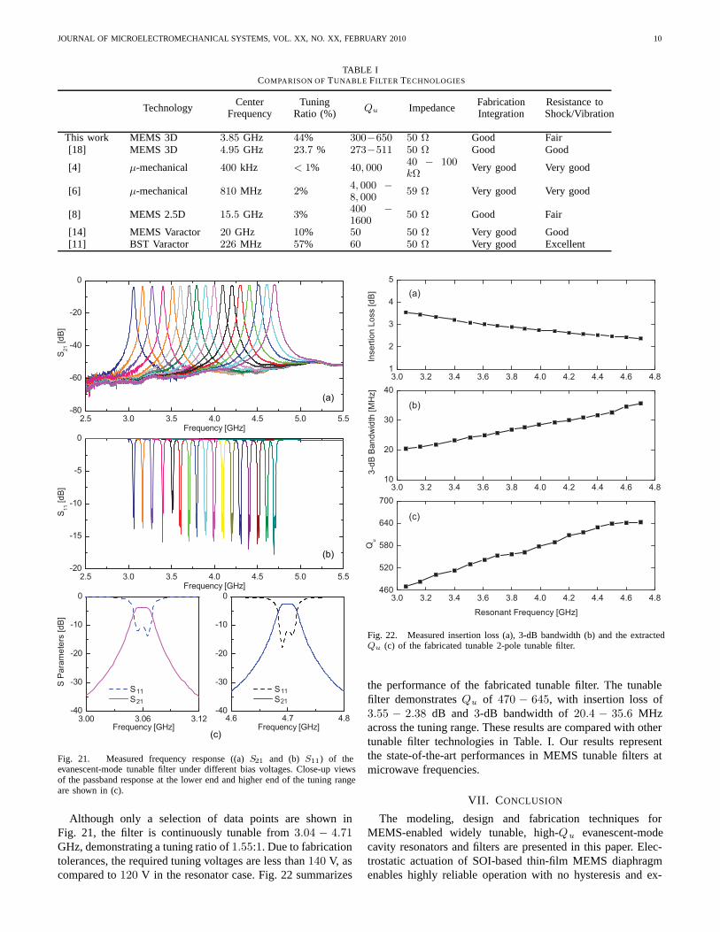
Although only a selection of data points are shown inFig. 21, the filter is continuously tunable from 3.04 − 4.71GHz, demonstrating a tuning ratio of 1.55:1. Due to fabricationtolerances, the required tuning voltages are less than 140 V, ascompared to 120 V in the resonator case. Fig. 22 summarizes
(a)
(b)
(c)
Fig. 22. Measured insertion loss (a), 3-dB bandwidth (b) and the extractedQu (c) of the fabricated tunable 2-pole tunable filter.
the performance of the fabricated tunable filter. The tunablefilter demonstrates Qu of 470 − 645, with insertion loss of3.55 − 2.38 dB and 3-dB bandwidth of 20.4 − 35.6 MHzacross the tuning range. These results are compared with othertunable filter technologies in Table. I. Our results representthe state-of-the-art performances in MEMS tunable filters atmicrowave frequencies.
VII. CONCLUSION
The modeling, design and fabrication techniques forMEMS-enabled widely tunable, high-Qu evanescent-modecavity resonators and filters are presented in this paper. Elec-trostatic actuation of SOI-based thin-film MEMS diaphragmenables highly reliable operation with no hysteresis and ex-

JOURNAL OF MICROELECTROMECHANICAL SYSTEMS, VOL. XX, NO. XX, FEBRUARY 2010 11
cellent mechanical stability. A continuously tunable resonatorfrom 1.9 to 5.0 GHz (2.6:1 tuning ratio) with Qu of 300−650is demonstrated. The required electrostatic voltage is less than120 V. A 2-pole continuously tunable filter is also designedand measured covering 3.04− 4.71 GHz (1.55:1 tuning ratio)with insertion loss of 3.55−2.38 dB for a 3-dB bandwidth of0.7%. Further advancement of the low-temperature bondingtechniques will result in even higher quality factors andreduced RF losses for the resonators and filters. Research onimproving the bonding technology is currently underway.
REFERENCES
[1] X. Liu, L. P. B. Katehi, W. J. Chappell, D. Peroulis, “A 3.4-6.2 GHzContinuously Tunable Electrostatic MEMS Resonator with Quality Factorof 460-530”, 2009 IEEE MTT-S International Microwave Symposium,Boston, MA USA, June 2009.
[2] H. Arslan, Cognitive Radio, Software Defined Radio, and AdaptiveWireless Systems, Springer, 2007.
[3] W. J. Keane, “YIG filters aid wide open receivers”, Microwave J., vol.17, no. 8, September 1980.
[4] K. Wang, C. T.-C. Nguyen, “High-order medium frequency microme-chanical electronic filters”, Journal of Microelectromechanical Systems ,vol.8, no.4, pp.534-556, December 1999
[5] S. Pourkamali, R. Abdolvand, G. K. Ho, F. Ayazi, “Electrostatically cou-pled micromechanical beam filters”, 17th IEEE International Conferenceon Micro Electro Mechanical Systems (MEMS), pp. 584-587, 2004
[6] H. Chandrahalim, D. Weinstein, L. F. Cheow, S. A. Bhave, “High-kdielectrically transduced MEMS thickness shear mode resonators andtunable channel-select RF filters”, Sensors and Actuators A, vol.136, no.2,pp. 527-539, 2007
[7] W. D. Yan, R. R. Mansour, “Micromachined Millimeter-wave RidgeWaveguide Filter with Embedded MEMS Tuning Elements,”, 2006 IEEEMTT-S Int. Microwave Symp. Dig., vol., no., pp.1290-1293, 11-16 June2006
[8] W. D. Yan, R. R. Mansour, “Tunable Dielectric Resonator Bandpass FilterWith Embedded MEMS Tuning Elements,”, IEEE Trans. MicrowaveTheory & Tech., vol.55, no.1, pp.154-160, Jan. 2007
[9] A. R. Brown, G. M. Rebeiz, “A varactor-tuned RF filter”, IEEE Trans.Microwave Theory & Tech., vol.48, no.7, pp.1157-1160, Jul 2000.
[10] F. A. Miranda, G. Subramanyam, F. W. van Keuls, R. R. Romanofsky,J. D. Warner, C. H. Mueller, “Design and development of ferroelectrictunable microwave components for Ku and K-band satellite communi-cation systems”, IEEE Trans. Microwave Theory & Tech., vol.48, no.7,pp.1181-1189, Jul 2000
[11] A. Tombak, J.-P. Maria, F. T. Ayguavives, Z. Jin, G. T. Stauf, A. I.Kingon, A. Mortazawi, “Voltage-controlled RF filters employing thin-filmbarium-strontium-titanate tunable capacitors”, IEEE Trans. MicrowaveTheory & Tech., vol.51, no.2, pp. 462-467, Feb. 2003
[12] J. Nath, D. Ghosh, J.-P. Maria, A. I. Kingon, W. Fathelbab, P. D.Franzon, M. B. Steer, “An electronically tunable microstrip bandpass filterusing thin-film Barium-Strontium-Titanate (BST) varactors”, IEEE Trans.Microwave Theory & Tech., vol.53, no.9, pp. 2707-2712, Sept. 2005
[13] D. Peroulis, S. Pacheco, K. Sarabandi, L. P. B. Katehi, “MEMS devicesfor high isolation switching and tunable filtering”, 2000 IEEE MTT-S Int.Microwave Symp. Dig., vol.2, no., pp.1217-1220 vol.2, 2000
[14] A. Abbaspour-Tamijani, L. Dussopt, G. M. Rebeiz, “Miniature andtunable filters using MEMS capacitors”, IEEE Trans. Microwave Theory& Tech., vol.51, no.7, pp. 1878-1885, July 2003
[15] A. Pothier, J.-C. Orlianges, G. Zheng, C. Champeaux, A. Catherinot, D.Cros, P. Blondy, J. Papapolymerou, “Low-loss 2-bit tunable bandpassfilters using MEMS DC contact switches”, IEEE Trans. MicrowaveTheory & Tech., vol.53, no.1, pp. 354-360, Jan. 2005
[16] S. M. Hou, J. H. Lang, A. H. Slocum, A. C. Weber, and J. R. White, “ AHigh-Q Widely Tunable Gigahertz Electromagnetic Cavity Resonator”, J.Microelectromech. Syst., vol. 15, no. 6, pp. 1540-1545, December 2006.
[17] H. Joshi, H. H. Sigmarsson, D. Peroulis, and W. J. Chappell, “HighlyLoaded Evanescent Cavities for Widely Tunable High-Q Filters”, 2007IEEE MTT-S Int. Microwave Symp. Dig., pp. 2133-2136, June 2007.
[18] S.-J. Park, I. Reines, and G. M. Rebeiz, “High-Q RF-MEMS tun-able evanescent-mode cavity filter”, 2008 IEEE MTT-S InternationalMicrowave Symposium, Boston, MA USA, June 2009.
[19] T.S. Low, W. Guo, “Modeling of a three-layer piezoelectric bimorphbeam with hysteresis”,J. Microelectromech. Syst., vol.4, no.4, pp.230-237,Dec 1995.
[20] E. Cattana, T. Haccarta, G. Velua, D. Remiensa, C. Bergaudb, L. Nicub,“Piezoelectric properties of PZT films for microcantilever”,Sensors andActuators A: Physical, Vol. 74, Issues 1-3, pp. 60-64, April 1999,
[21] S. Trolier-McKinstry, P. Muralt, “Thin Film Piezoelectrics for MEMS”,Journal of Electroceramics, Vol. 12, no. 1-2, January 2004.
[22] I. Mayergoyz, G.Bertotti, The Science of Hysteresis, Elsevier, 2005[23] T. A. Schwarz, and L. P. B. Katehi, “A Micromachined Evanescent
Mode Resonator”, 1999 European Microwave Conference Dig., vol. 2,pp. 403-406, October 1999.
[24] X. Gong, A. Margomenos, B. Liu, S. Hajela, L. P. B. Katehi and W.J. Chappell, “Precision Fabrication Techniques and Analysis on Hihg-Q Evanescent-Mode Resonators and Filters of Different Geometries,”IEEE Trans. Microwave Theory & Tech., vol. 52, no. 11, pp. 2557-2566,November 2004.
[25] R. G. Carter, J. Feng, U. Becker, “Calculation of the Properties of Reen-trant Cylindrical Cavity Resonators”, IEEE Trans. Microwave Theory &Tech., vol. 55, no. 12, pp. 2531-2538, December 2007.
[26] High Frequency Structure Simulator, Ansoft Cooperation.http://www.ansoft.com/products/hf/hfss/
[27] G. M. Rebeiz, RF MEMS, Theory, Design and Technology, New York:J. Wiley & Sons, 2003.
[28] Rogers Corporation,TMM R© Thermoset Microwave Laminates,http://www.rogerscorp.com/acm/products/14/TMM-Thermoset-Microwave-Laminates-Thermoset-ceramic-loaded-plastic.aspx
[29] W. C. Young, R. J. Roark, R. G. Budynas, Roark’s Formulas for Stressand Strain, 7th Ed., New York: McGraw-Hills, 2002.
[30] S. D. Senturia, Microsystem Design, Kluwer Academic Pub., 2000.[31] F. A. McClintock, A. S. Argon, Mechanical Behavior of Materials,
TechBooks (reprinted by arrangement with Addison-Wesley PublishingCompany, Inc.), Fairfax, VA, 1965, Chapter 12, pp. 432-434 and Chapter19, pp 640-644.
[32] X. Yan, W.L. Brown, Y. Li, J. Papapolymerou, C. Palego, J. C. M.Hwang, R. P. Vinci, “Anelastic Stress Relaxation in Gold Films and ItsImpact on Restoring Forces in MEMS Devices”, J. Microelectromechan-ical Syst., vol.18, no.3, pp.570-576, June 2009
[33] Creative Materials Inc.118-09A/B-187 Solvent-Resistant Electrically Conductive Inkhttp://server.creativematerials.com/datasheets/DS 118 09A B187.pdf
[34] Coventor Inc. http://www.coventor.com[35] H. H. Sigmarsson, A. Christianson, H. Joshi, S. Moon, D. Peroulis,
W. J. Chappell, “In-Situ Control of Tunable Evanescent-Mode CavityFilters Using Differential Mode Monitoring”, 2008 IEEE MTT-S Interna-tional Microwave Symposium, Boston, MA USA, June 2009.
[36] G. L. Matthaei, L. Young, E. M. T. Jones, Microwave Filters, Impedance-Matching Networks and Coupling Structures, New York: McGraw-Hill,1964.
Xiaoguang Liu (S’07) received the Bachelor’s de-gree in electrical engineering from Zhejiang Uni-versity, China in 2004 and is currently workingtoward the Ph.D. degree at Purdue University, WestLafayette, IN.
His research interests include novel RF MEMSdevices and high-Q tunable filters for reconfigurableradio frontends.
He is the recipient of the 2009 Antenna andPropagation Society Graduate Research Fellowship.

JOURNAL OF MICROELECTROMECHANICAL SYSTEMS, VOL. XX, NO. XX, FEBRUARY 2010 12
Linda P. B. Katehi (S’81-M’84-SM’89-F’95) is cur-rently the Chancellor at the University of Californiaat Davis. She has authored or coauthored over 600papers published in refereed journals and symposiaproceedings, as well as nine book chapters. Sheholds 13 U.S. patents. Her research is focused on thedevelopment and characterization of 3-D integrationand packaging of integrated circuits with a particularemphasis on MEMS devices, high-Q evanescentmode filters, and the theoretical and experimentalstudy of planar circuits for hybrid-monolithic and
monolithic oscillators, amplifiers, and mixer applications.Prof. Katehi is a member of the National Academy of Engineering, the
Nominations Committee for the National Medal of Technology, the KauffmanNational Panel for Entrepreneurship, the National Science Foundation (NSF)Advisory Committee to the Engineering Directorate, and numerous otherengineering and scientific committees. She has been the recipient of numerousnational and international technical awards and to distinctions as an educator.
William J. Chappell (S’98-M’02) received theB.S.E.E., M.S.E.E., and Ph.D. degrees from TheUniversity of Michigan at Ann Arbor, in 1998, 2000,and 2002, respectively.
He is currently an Associate Professor with theElectrical and Computer Engineering Department,Purdue University, West Lafayette, IN, and is also amember of the Birck Nanotechnology Center and theCenter for Wireless Systems and Applications. Hisresearch focus is on advanced applications of RF andmicrowave components. He has been involved with
numerous Defense Advanced Research Projects Agency (DARPA) projectsinvolved in advanced packaging and materials processing for microwaveapplications. His research sponsors include Homeland Security AdvancedResearch Projects Agency (HSARPA), Office of Naval Research (ONR),National Science Foundation (NSF), the State of Indiana, Communications-Electronics Research, Development, and Engineering Center (CERDEC), U.S.Army Research Office (ARO), as well as industry sponsors. His research groupuses electromagnetic analysis, unique processing of materials, and advanceddesign to create novel microwave components. His specific research interestsare the application of very high-quality and tunable components utilizingpackage-scale multilayer components. In addition, he is involved with high-power RF systems, packages, and applications.
Dr. Chappell was the recipient of the URSI Young Scientist Award, theJoel Spira Teaching Excellence Award, and the Eta Kappa Nu 2006 Teacherof the Year Award presented by Purdue University.
Dimitrios Peroulis (S’99-M’04) received theDiploma degree in electrical and computer engi-neering from the National Technical University ofAthens, Athens, Greece, in 1998, and the M.S.E.E.and Ph.D. degrees in electrical engineering from TheUniversity of Michigan, Ann Arbor, in 1999 and2003, respectively.
He is currently an Associate Professor with theSchool of Electrical and Computer Engineering,Purdue University, West Lafayette, IN. His researchwork is focused on microelectromechanical systems
(MEMS) for multifunctional communications systems and sensors. His groupis currently part of two research centers funded by DARPA (IMPACT center)and the National Nuclear Security Administration (PRISM center) that arefocused on MEMS failure mechanisms and reliability.


![Optical Surface Microtraps based on Evanescent Waves · Optical Surface Microtraps based on Evanescent Waves Dissertation zur Erlangung des Doktorgrades an der ... [Fol02]. While](https://img.dokumen.tips/doc/110x75/5bdee43809d3f2647f8b63e5/optical-surface-microtraps-based-on-evanescent-optical-surface-microtraps-based.jpg)