Embed Size (px)
Citation preview
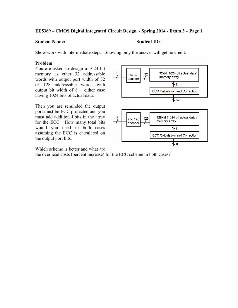
EE5369 – CMOS Digital Integrated Circuit Design - Spring 2014 - Exam 3 – Page 1 Student Name:______________________________ Student ID: _______________ Show work with intermediate steps. Showing only the answer will get no credit. Problem You are asked to design a 1024 bit memory as ether 32 addressable words with output port width of 32 or 128 addressable words with output bit width of 8 – either case having 1024 bits of actual data. Then you are reminded the output port must be ECC protected and you must add additional bits in the array for the ECC. How many total bits would you need in both cases assuming the ECC is calculated on the output port bits. Which scheme is better and what are the overhead costs (percent increase) for the ECC scheme in both cases?
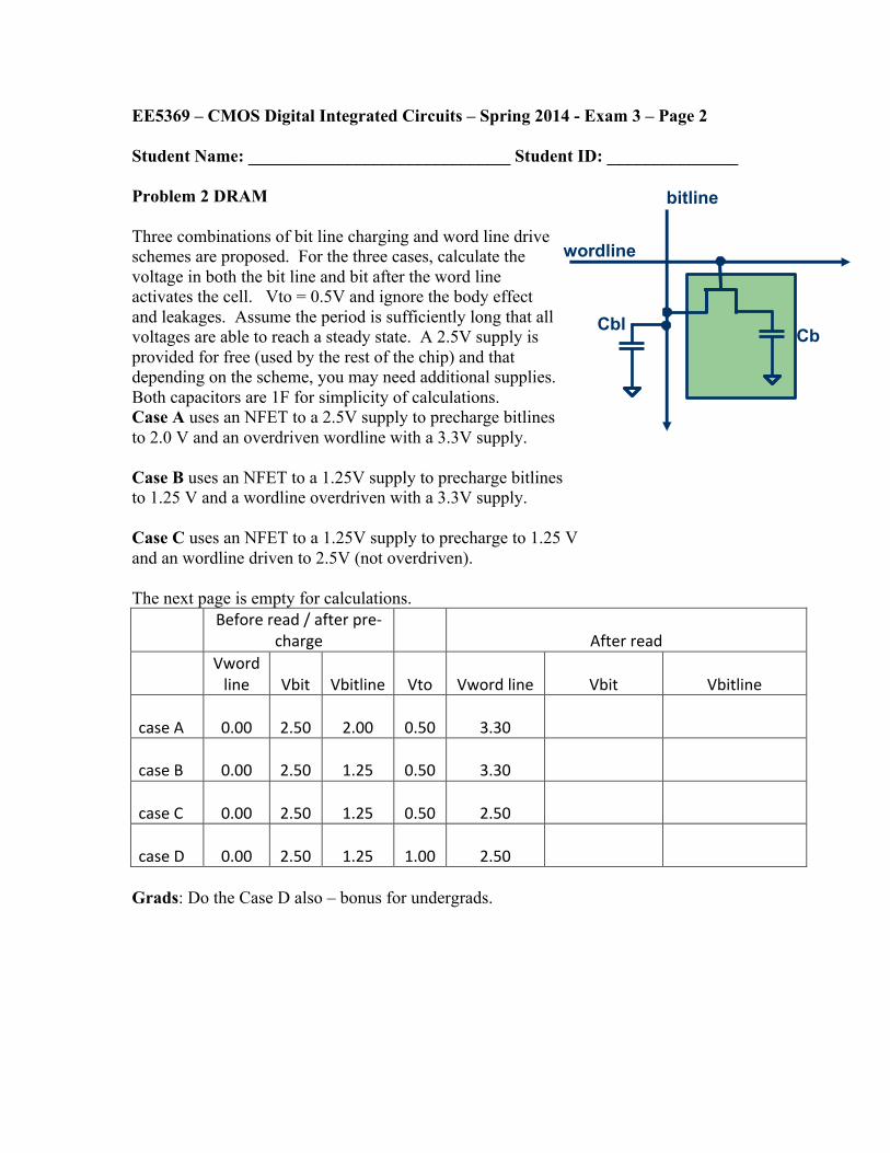
EE5369 – CMOS Digital Integrated Circuits – Spring 2014 - Exam 3 – Page 2 Student Name: ______________________________ Student ID: _______________ Problem 2 DRAM Three combinations of bit line charging and word line drive schemes are proposed. For the three cases, calculate the voltage in both the bit line and bit after the word line activates the cell. Vto = 0.5V and ignore the body effect and leakages. Assume the period is sufficiently long that all voltages are able to reach a steady state. A 2.5V supply is provided for free (used by the rest of the chip) and that depending on the scheme, you may need additional supplies. Both capacitors are 1F for simplicity of calculations. Case A uses an NFET to a 2.5V supply to precharge bitlines to 2.0 V and an overdriven wordline with a 3.3V supply. Case B uses an NFET to a 1.25V supply to precharge bitlines to 1.25 V and a wordline overdriven with a 3.3V supply. Case C uses an NFET to a 1.25V supply to precharge to 1.25 V and an wordline driven to 2.5V (not overdriven). The next page is empty for calculations.
Before read / after pre-‐
charge After read
Vword line Vbit Vbitline Vto Vword line Vbit Vbitline
case A 0.00 2.50 2.00 0.50 3.30
case B 0.00 2.50 1.25 0.50 3.30
case C 0.00 2.50 1.25 0.50 2.50
case D 0.00 2.50 1.25 1.00 2.50 Grads: Do the Case D also – bonus for undergrads.
Cbl Cb
wordline
bitline
EE5369 – Digital Integrated Circuits - Fall 2013 - Exam 3 – Page 3 Student Name:______________________________ Student ID: _______________ Problem 2 continued

EE5369 – Digital Integrated Circuits - Spring 2014 - Exam 3 – Page 4 Student Name:______________________________ Student ID: _______________ Problem 3 Three SRAM cells are suggested. What are the relative advantages and disadvantages of each in terms of power, performance, and area (cost). Assume resistors are 20% of the area of transistors and that the mobilities of NFETs are twice that of PFETs.