Embed Size (px)
Citation preview
EE40 Lec 18EE40 Lec 18
Diode CircuitsDiode Circuits
Reading Chap 10 of HambleReading: Chap. 10 of HambleySupplement Reading on Diode Circuits
http://www inst eecs berkeley edu/~ee40/fa09/handouts/EE40 MOS Circuit pdf
Slide 1EE40 Fall 2009 Prof. Cheung
http://www.inst.eecs.berkeley.edu/ ee40/fa09/handouts/EE40_MOS_Circuit.pdf
Diodes Circuits
–Load Line Analysisy–Analysis of Diode Circuits by
assumed statesassumed states–Diode Logic Circuits–Wave Shaping Circuits
Rectifying Circuits–Rectifying Circuits
Slide 2EE40 Fall 2009 Prof. Cheung

SOLVING CIRCUITS WITH NONLINEAR ELEMENTS
Look at circuits with a nonlinear element like this:IL INL
Linear circuit
L+VL
Nonlinear element
NL+VNL
- -
A nonlinear element with its own I-V relationship, attached to a linear circuit with its own I-V relationship.
1. IL = fL(VL) (linear circuit I-V relationship)2. INL = gNL(VNL) (nonlinear element I-V relationship)3. INL = -IL4. VNL = VL
Slide 3EE40 Fall 2009 Prof. Cheung
4. VNL VL

SOLVING CIRCUITS WITH NONLINEAR ELEMENTS
The 4 equations can be reduced to 2 equations in INL and VNL
INL = -fL(VNL) - the linear “loadline” INL = gNL(VNL)
which we can equate and solve for VNL,
or…graph the two equations and solve for the intersection.
Slide 4EE40 Fall 2009 Prof. Cheung

EXAMPLE
+INL+
1 kΩ
+I Given : I0 = 10-15 A.+
- VNL
+
_2 V VL_
ILGiven : I0 10 A.Find VNL
1. IL = (VL- 2) / 1000
( )1e10I 026.0/NLV15NL −= −2.
3 I I Substitute 1 and 2 in 33. INL = -IL
4. VNL = VL( ) [ ]1000/)2V(1e10 NL
15 026.0/NLV −−=−−
Substitute 1 and 2 in 3
Slide 5EE40 Fall 2009 Prof. Cheung
Solve by iteration, VNL ~ 0.725V

0.004linear
Graphical Solution
0.003
0.0035linear
nonlinear
0.002
0.0025 Loadline: I= - (V-2)/1000
0.001
0.0015
I_N
L
0
0.0005Diode I-V
0.725V
-0.001
-0.0005
0.725V
Slide 6EE40 Fall 2009 Prof. Cheung
-1 -0.5 0 0.5 1
V_NL
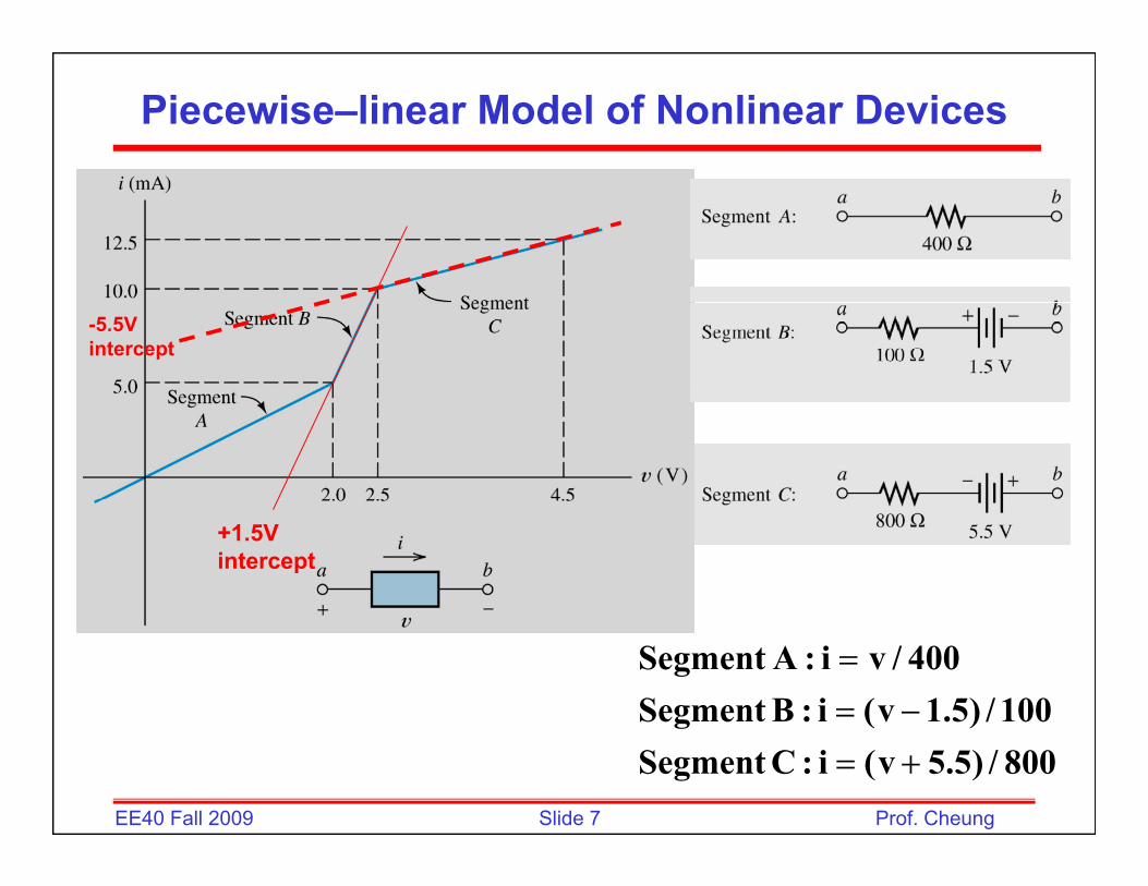
Piecewise–linear Model of Nonlinear Devices
-5.5Vintercept
+1.5Vintercept
100/)5.1v(i:BSegment400/vi:ASegment−=
=
Slide 7EE40 Fall 2009 Prof. Cheung
800/)5.5v(i:CSegment)(g
+=

Ideal Diode Model of PN Diode
ID (A)ID +ID
Circuit symbol I-V characteristic Switch model
forward biasVD
+VD–
reverse bias VD (V)–
Diode behaves like a switch: • closed in forward bias mode • open in reverse bias mode
Slide 8EE40 Fall 2009 Prof. Cheung
•used when voltage of interest >> 0.6V

Piecewise Linear Model
ID + +ID
Circuit symbol I-V characteristic Switch modelID (A)
VDVDforward bias
+− VDon
VD (V)– –reverse bias
VDon
For a Si pn diode, VDon ≅ 0.6 V
Diode behaves like a voltage source in series with a switch: • closed in forward bias mode
i bi d
Slide 9EE40 Fall 2009 Prof. Cheung
• open in reverse bias mode

Zener DiodeA Zener diode is designed to operate in the breakdown mode.
ID (A)(l k ) t ID (A)
V (V)
reverse (leakage) current
forward current
breakdown voltage VBD VD (V)
R tvs(t) >15V for all t
integratedi it
R
+v (t)
+v (t)
Slide 10EE40 Fall 2009 Prof. Cheung
circuitVBD = 15V
vs(t)–
vo(t)–
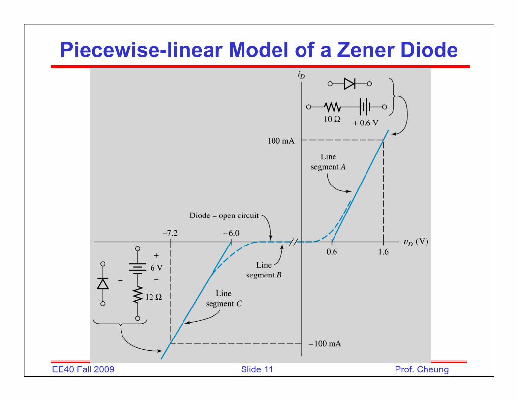
Piecewise-linear Model of a Zener Diode
Slide 11EE40 Fall 2009 Prof. Cheung

Diode Circuit Analysis by Assumed Diode States
•1) Specify Ideal Diode Model or Piecewise-Linear Diode Model
ID (A) ID (A)
reverse biasforward bias
VD (V)reverse bias
forward bias
•2) Each diode can be ON or OFF
VD (V)VDon
•3) Circuit containing n diodes will have 2n states•4) The combination of states that works for ALL di d ( i t t ith KVL d KCL) ill b th
Slide 12EE40 Fall 2009 Prof. Cheung
diodes (consistent with KVL and KCL) will be the solution

Example Analysis by assumed Diode States
D1=on D2=on×1.75mA
0.5mA
D1=off D2=on +10 +3
D1=on D2=off
+30
×D1=off D2=off
+10×
√
D1=on D2=off +3+6
Slide 13EE40 Fall 2009 Prof. Cheung
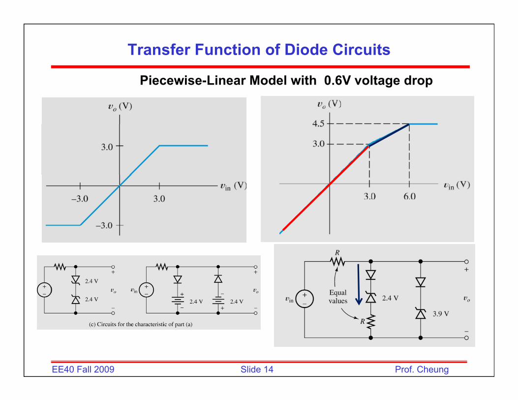
Transfer Function of Diode Circuits
Piecewise-Linear Model with 0.6V voltage drop
Slide 14EE40 Fall 2009 Prof. Cheung
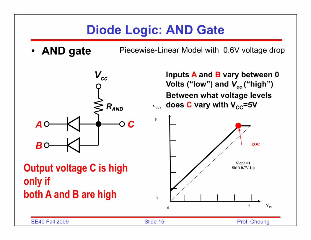
Diode Logic: AND Gate• AND gate
V Inputs A and B vary between 0
Piecewise-Linear Model with 0.6V voltage drop
R
Vcc Inputs A and B vary between 0 Volts (“low”) and Vcc (“high”)Between what voltage levels does C vary with V =5VV
A
RAND
C
does C vary with VCC=5VVOUT
5
BSlope =1
EOC
O t t lt C i hi h Shift 0.7V UpOutput voltage C is high only if both A and B are high
Slide 15EE40 Fall 2009 Prof. Cheung
VIN0 5
0both A and B are high

Diode Logic: OR Gate• OR gate
Inputs A and B vary between 0 V lt (“l ”) d V (“hi h”)
Piecewise-Linear Model with 0.6V voltage drop
A
B C
Volts (“low”) and Vcc (“high”)Between what voltage levels does C vary with VCC=5V?
BROR
CVOUT
5
Output voltage C is high if
EOC
Output voltage C is high if either (or both) A and B are high
Slope =1Shift 0.7V Down
Slide 16EE40 Fall 2009 Prof. Cheung
VIN0 5
0
0.7V

Diode Logic: Incompatibility and Decay
AND gate OR gate
Signal Decays with each stage (Not regenerative)
output voltage is high only if both A and B are high
output voltage is high if either (or both) A and B are high
Vcc
RAND
A
B CA CAND
BROR
COR
B0.6V drop
Slide 17EE40 Fall 2009 Prof. Cheung
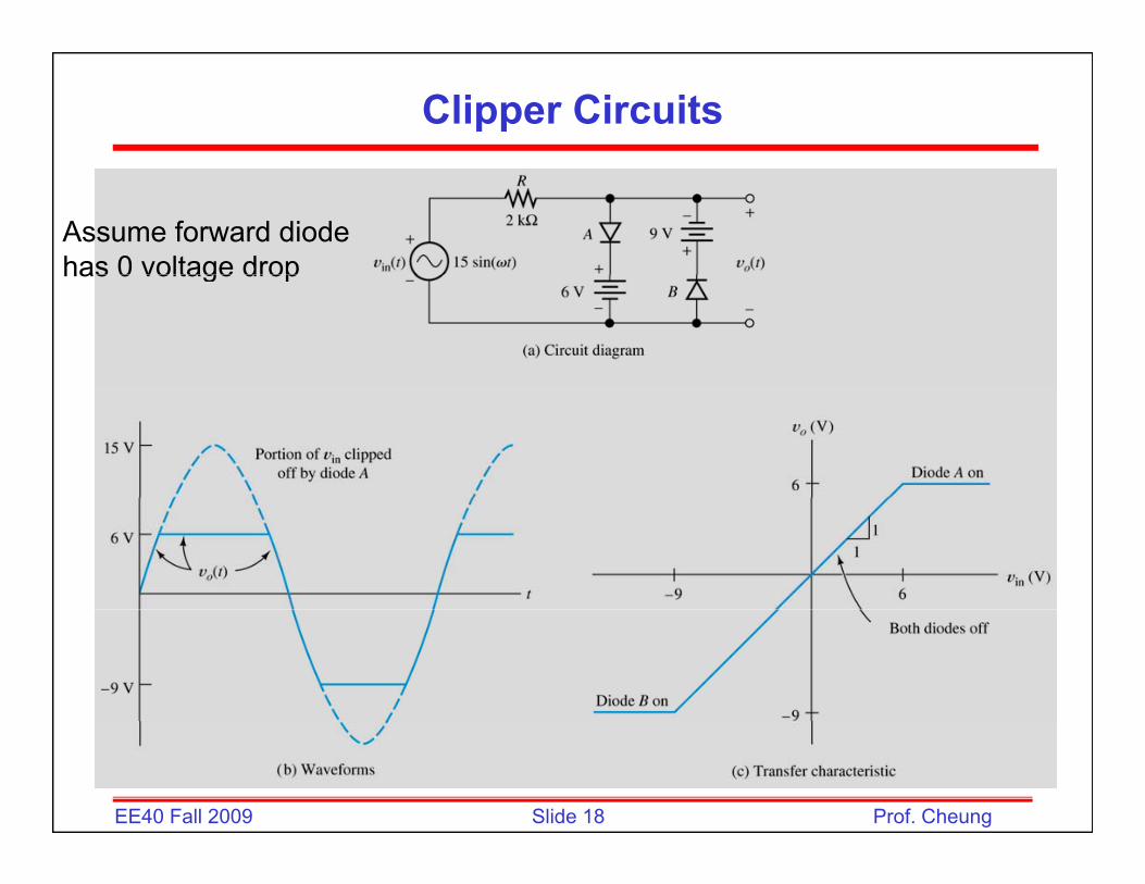
Clipper Circuits
Assume forward diode has 0 voltage drophas 0 voltage drop
Slide 18EE40 Fall 2009 Prof. Cheung
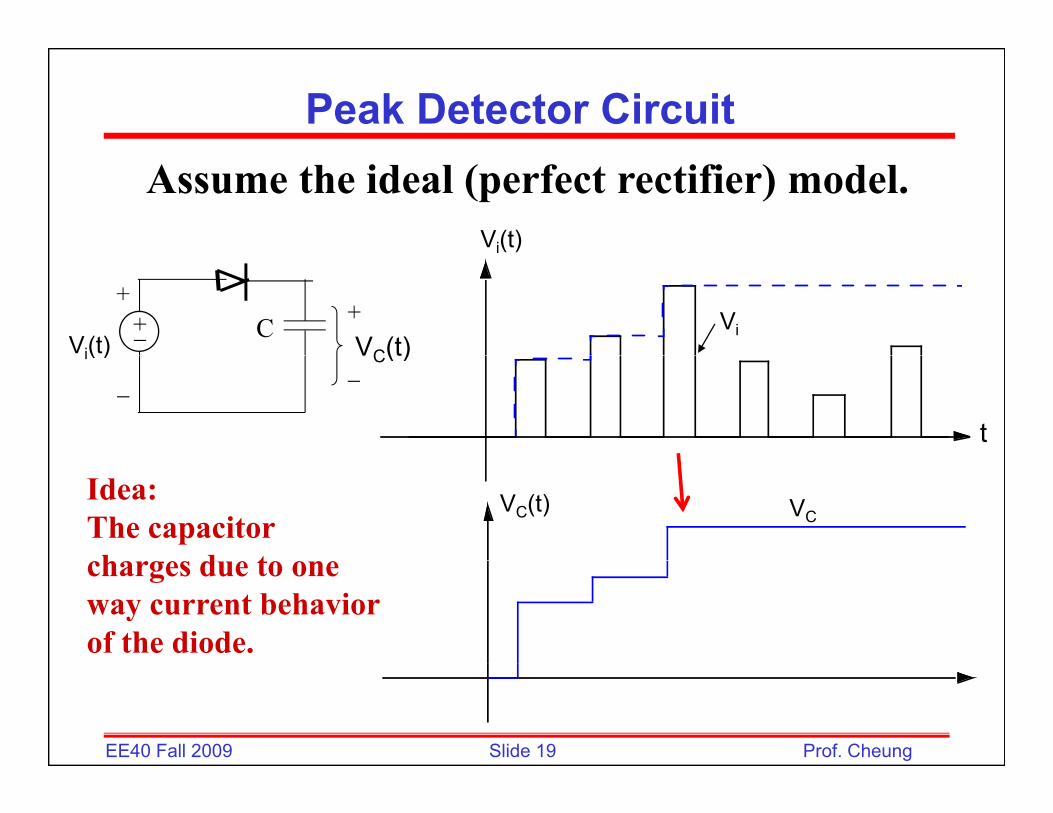
Peak Detector Circuit
Vi(t)
Assume the ideal (perfect rectifier) model.
+
VC(t)Vi(t)+C Vi+−
−
VC(t)i( )−
t
VC(t) VCIdea: The capacitor h d tcharges due to one
way current behavior of the diode.
Slide 19EE40 Fall 2009 Prof. Cheung
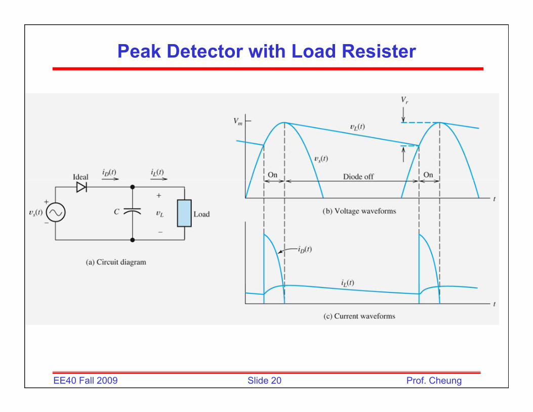
Peak Detector with Load Resister
Slide 20EE40 Fall 2009 Prof. Cheung

Level Shift Circuit
- VC + VIN VC
VOUT
+
VIN
+
C t
--
V = V + VVOUT 1 3
VOUT = VC+ VINt
21) Diode =open, VC=0, VOUT = VIN2) Diode =short, VC= -VIN , VOUT=03) Diode =open V = V (min) V = V +V
Slide 21EE40 Fall 2009 Prof. Cheung
3) Diode =open, VC= -VIN (min) , VOUT= VIN+VC,
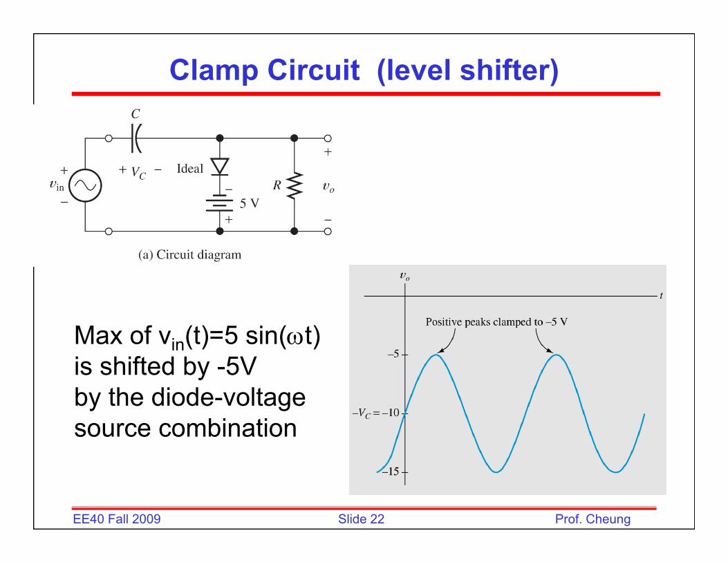
Clamp Circuit (level shifter)
Max of vin(t)=5 sin(ωt)is shifted by -5V b h di d lby the diode-voltage source combination
Slide 22EE40 Fall 2009 Prof. Cheung
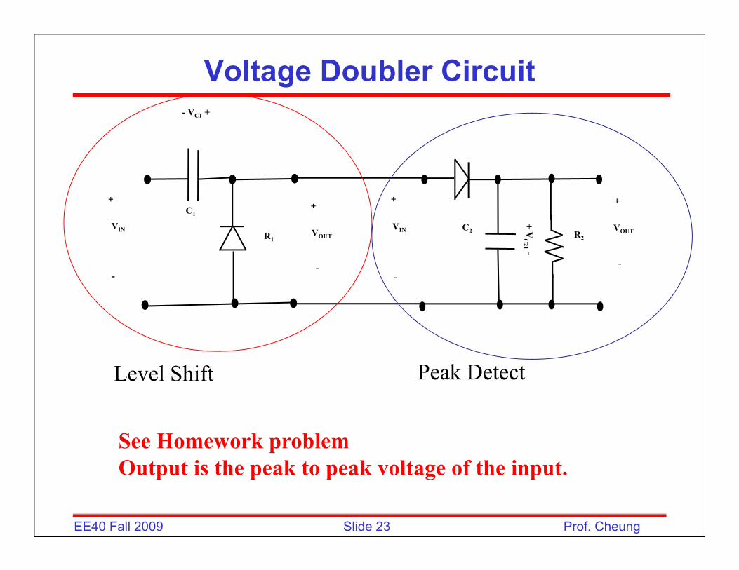
Voltage Doubler Circuit- VC1 +
+ VC
21
R2VOUT
+
VIN
+
C2R1
VOUT
+
VIN
+
C1-
--
--
Level Shift Peak Detect
See Homework problemOutput is the peak to peak voltage of the input
Slide 23EE40 Fall 2009 Prof. Cheung
Output is the peak to peak voltage of the input.

Half Wave Rectifier Equivalent circuit
V >0.6V, diode = short circuitV = VI - 0 6Vo VI 0.6
V < 0.6V, diode = open circuitpVo =0
Slide 24EE40 Fall 2009 Prof. Cheung
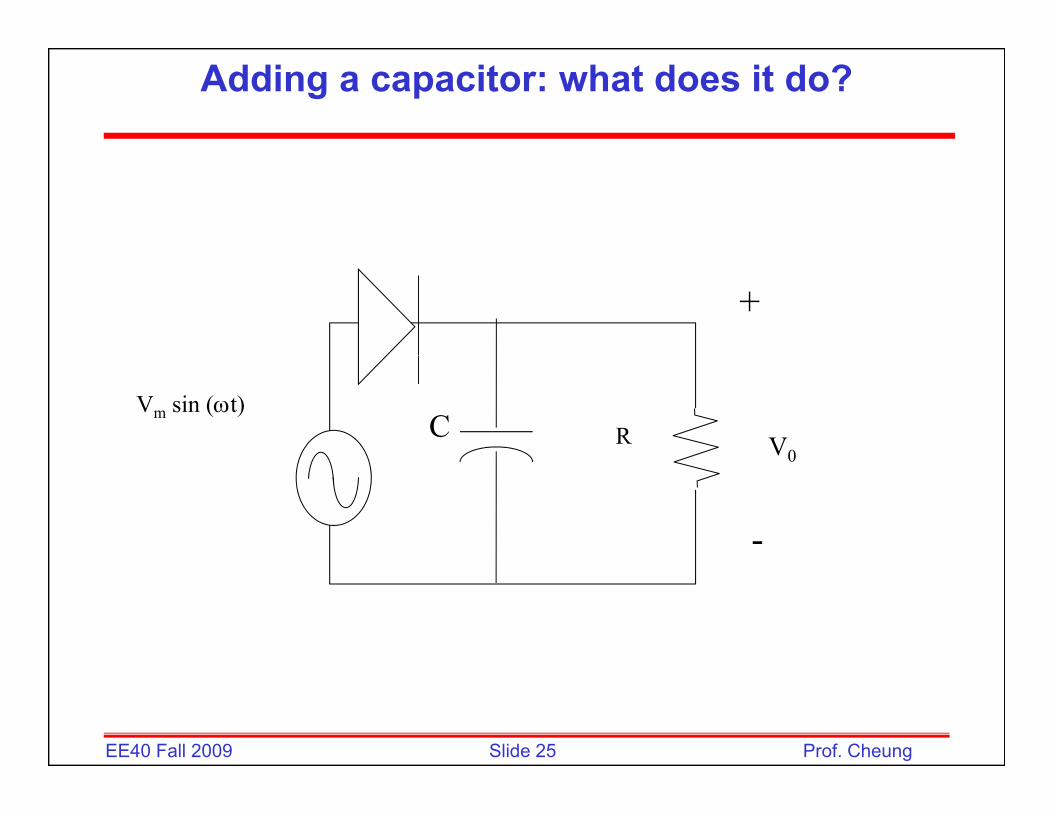
Adding a capacitor: what does it do?
+
Vm sin (ωt)R V0
C0
-
Slide 25EE40 Fall 2009 Prof. Cheung
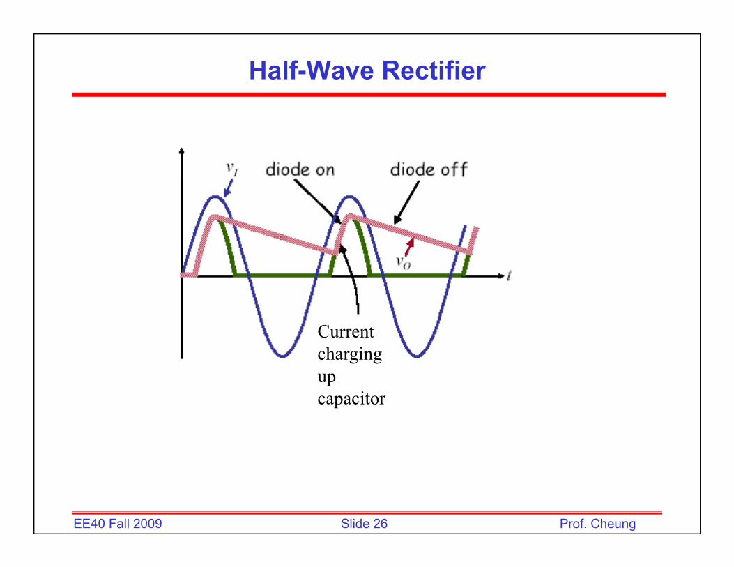
Half-Wave Rectifier
Current charging up capacitor
Slide 26EE40 Fall 2009 Prof. Cheung

Full Wave Rectifier
Slide 27EE40 Fall 2009 Prof. Cheung

Small –Signal Linear Equivalent CircuitSuppose the nonlinear device has the functional dependence I = i(v) is biased with a DC voltage vG at the Q-point (quiescent point) A small differential voltage ∆v ispoint (quiescent point). A small differential voltage ∆v is added on top of vG. Using Taylor series expansion
.........vdi)v(i)vv(i QQ +∆•+=∆+ .........vdv
)v(i)vv(iQv
QQ +∆+∆+
We can define a dynamic resistance r at the Q point
di1r ≡
i Tangent line
vi ∆∆
Qvdv∆i
Slide 28EE40 Fall 2009 Prof. Cheung
ri ≅∆
vvG
∆v

Small –Signal Model of Diode
Q2∆i
Q1
∆i
rvi ∆
≅∆
∆i
Slide 29EE40 Fall 2009 Prof. Cheung
∆v ∆v

Small –Signal Model Example
VC and RCDetermines rd atdQ point of diode
Slide 30EE40 Fall 2009 Prof. Cheung

Small –Signal Model Example
The large capacitors and DC bias source are effective shortsfor the ac signal in small-signal circuits
Slide 31EE40 Fall 2009 Prof. Cheung
for the ac signal in small signal circuits* See Hambley for an application of voltage controlled Attenuator