Embed Size (px)
Citation preview
EE254L - Introduction to Digital Circuits
ee254l_timing.fm [Revised: 7/21/14] 1/16
Timing Analysi s and Timing Constraints
1. Synopsis:
The objective of this lab is to make you familiar with two critical reports produced by the Xilinx
ISE during your design synthesis and implementation. The lab introduces you to timing constraints
and uses a division-by-subtraction example to illustrate “packing” more computations per clock to
utilize the clock period fully and to reduce the number of clocks needed for the complete opera-
tion.
An easy to read reference is: http://www2.units.it/marsi/elettronica2/lucidi/XSTsynthesis.ppt
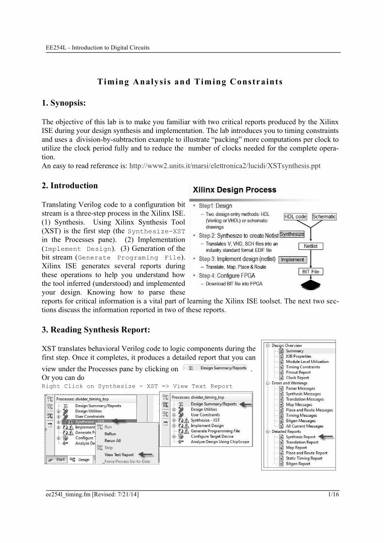
2. Introduction
Translating Verilog code to a configuration bit
stream is a three-step process in the Xilinx ISE.
(1) Synthesis. Using Xilinx Synthesis Tool
(XST) is the first step (the Synthesize-XST
in the Processes pane). (2) Implementation
(Implement Design). (3) Generation of the
bit stream (Generate Programing File).
Xilinx ISE generates several reports during
these operations to help you understand how
the tool inferred (understood) and implemented
your design. Knowing how to parse these
reports for critical information is a vital part of learning the Xilinx ISE toolset. The next two sec-
tions discuss the information reported in two of these reports.
3. Reading Synthesis Report:
XST translates behavioral Verilog code to logic components during the
first step. Once it completes, it produces a detailed report that you can
view under the Processes pane by clicking on .
Or you can do Right Click on Synthesize - XST => View Text Report
EE254L - Introduction to Digital Circuits
ee254l_timing.fm [Revised: 7/21/14] 2/16
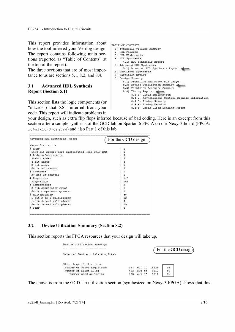
This report provides information about
how the tool inferred your Verilog design.
The report contains following main sec-
tions (reported as “Table of Contents” at
the top of the report).
The three sections that are of most impor-
tance to us are sections 5.1, 8.2, and 8.4.
3.1 Advanced HDL Synthesis
Report (Section 5.1)
This section lists the logic components (or
“macros”) that XST inferred from your
code. This report will indicate problems in
your design, such as extra flip flops inferred because of bad coding. Here is an excerpt from this
section after a sample synthesis of the GCD lab on Spartan 6 FPGA on our Nexys3 board (FPGA:
xc6slx16-3-csg324) and also Part 1 of this lab.
3.2 Device Utilization Summary (Section 8.2)
This section reports the FPGA resources that your design will take up.
The above is from the GCD lab utilization section (synthesized on Nexys3 FPGA) shows that this
For the GCD design
For the GCD design
EE254L - Introduction to Digital Circuits
ee254l_timing.fm [Revised: 7/21/14] 3/16
design takes 1% of the available registers in the FPGA. A design that takes more resources than
the FPGA has can not fit into the FPGA
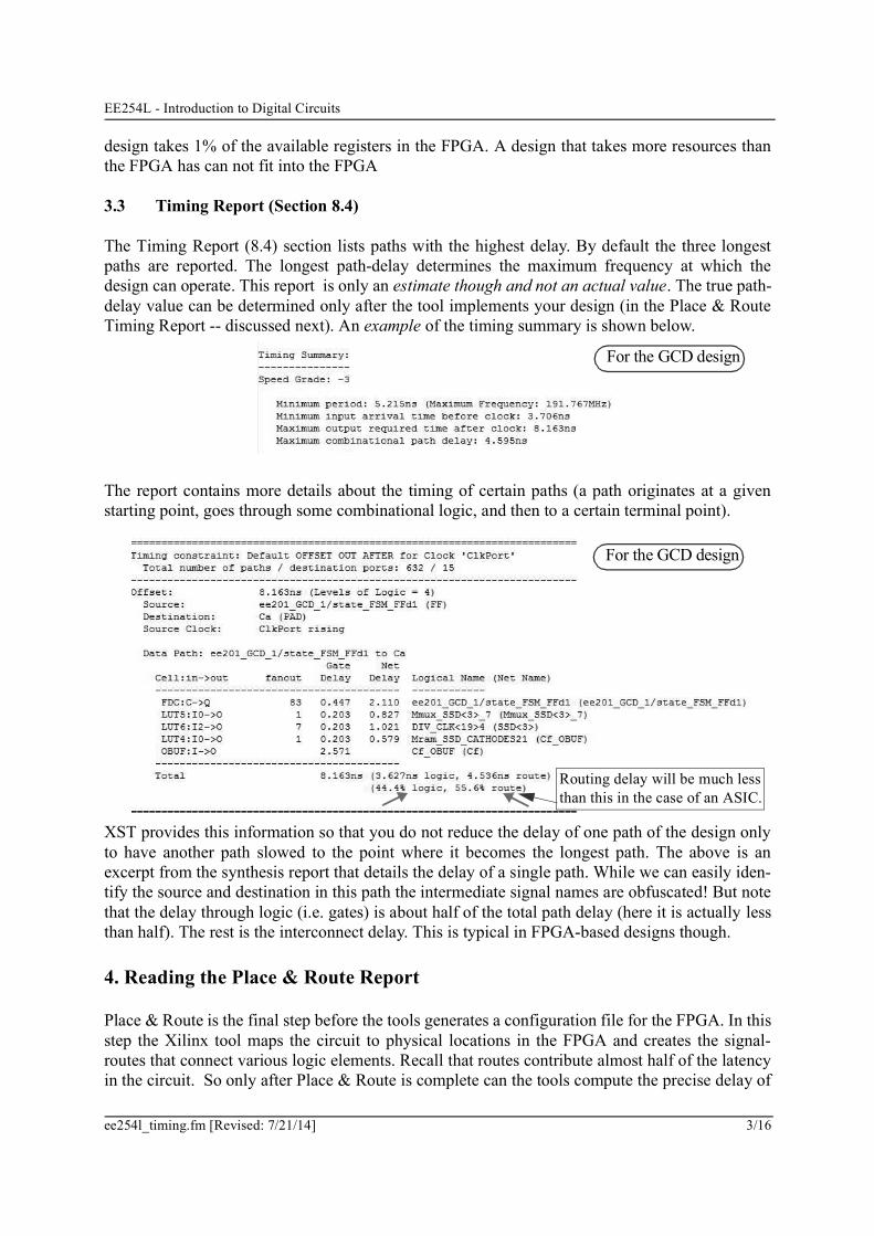
3.3 Timing Report (Section 8.4)
The Timing Report (8.4) section lists paths with the highest delay. By default the three longest
paths are reported. The longest path-delay determines the maximum frequency at which the
design can operate. This report is only an estimate though and not an actual value. The true path-
delay value can be determined only after the tool implements your design (in the Place & Route
Timing Report -- discussed next). An example of the timing summary is shown below.
The report contains more details about the timing of certain paths (a path originates at a given
starting point, goes through some combinational logic, and then to a certain terminal point).
XST provides this information so that you do not reduce the delay of one path of the design only
to have another path slowed to the point where it becomes the longest path. The above is an
excerpt from the synthesis report that details the delay of a single path. While we can easily iden-
tify the source and destination in this path the intermediate signal names are obfuscated! But note
that the delay through logic (i.e. gates) is about half of the total path delay (here it is actually less
than half). The rest is the interconnect delay. This is typical in FPGA-based designs though.
4. Reading the Place & Route Report
Place & Route is the final step before the tools generates a configuration file for the FPGA. In this
step the Xilinx tool maps the circuit to physical locations in the FPGA and creates the signal-
routes that connect various logic elements. Recall that routes contribute almost half of the latency
in the circuit. So only after Place & Route is complete can the tools compute the precise delay of
For the GCD design
Routing delay will be much less
than this in the case of an ASIC.
For the GCD design
EE254L - Introduction to Digital Circuits
ee254l_timing.fm [Revised: 7/21/14] 4/16
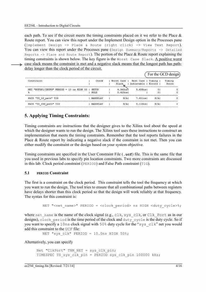
each path. To see if the circuit meets the timing constraints placed on it we refer to the Place &
Route report. You can view this report under the Implement Design option in the Processes pane
(Implement Design -> Place & Route (right click) -> View Text Report).
You can view this report under the Processes pane (Design Summary/Reports -> Detailed
Reports -> Place and Route Report). The portion of the Place & Route report explaining the
timing constraints is shown below. The key figure is the Worst Case Slack. A positive worst
case slack means the constraint is met and a negative slack means that the longest path has path-
delay longer than the clock period of the circuit.
5. Applying Timing Constraints:
Timing constraints are instructions that the designer gives to the Xilinx tool about the speed at
which the designer wants to run the design. The Xilinx tool uses these instructions to construct an
implementation that meets the timing constraints. Remember that the tool reports failures in the
Place & Route report by indicating a negative slack if the constraint is not met. Then you can
either modify the constraint or the design based on your system objective.
Timing constraints are specified in the User Constraint File (.ucf) file. This is the same file that
you used in previous labs to specify pin location constraints. Two more constraints are discussed
in this lab: Clock period constraint (PERIOD) and False Path constraint (TIG).
5.1 PERIOD Constraint
The first is a constraint on the clock period. This constraint tells the tool the frequency at which
you want to run the design. The tool tries to ensure that all combinational paths between registers
have delays shorter than this clock period so that the design will work reliably at that frequency.
The syntax for this constraint is:
NET "<net_name>" PERIOD = <clock_period> ns HIGH <duty_cycle>%;
where net_name is the name of the clock signal (e.g., clk, sys_clk, or Clk_Port as in our
designs), clock_period is the time period of the clock and duty_cycle is the duty cycle. So if
you want to specify a 10ns clock signal with 50% duty cycle for the “sys_clk” net you would
add this constraint to the UCF file:NET "sys_clk" PERIOD = 10.0ns HIGH 50%;
Alternatively, you can specify
Net "ClkPort" TNM_NET = sys_clk_pin;
TIMESPEC TS_sys_clk_pin = PERIOD sys_clk_pin 100000 kHz;
For the GCD design

EE254L - Introduction to Digital Circuits
ee254l_timing.fm [Revised: 7/21/14] 5/16
5.2 TIG Constraint
The second constraint that we use, instructs the tool to ignore the signal(s) when determining the
timing path. These paths are called “false paths”. To instruct the tool to ignore an input (switches
or buttons) signal the syntax is:
PIN "Sw1" TIG;
TIG stands for Timing Ignore Group. By assigning a signal to a TIG the tool ignores any timing
paths involving this signal. You would declare all other inputs (switches and buttons) as belong-
ing to a TIG using the above syntax.
For output (LEDs and SSDs) signals you cannot use the above syntax (a limitation of the Xilinx
tool). Instead you must first assign these signals to a new timing group. Then you must instruct
the tool to ignore the path timing issues that terminate to these signals. If your design uses only
two LEDs (i.e. Ld1 & Ld2) then the syntax would be:
NET "Ld1" TNM_NET = "LED_GROUP";
NET "Ld2" TNM_NET = "LED_GROUP";
TIMESPEC "TS_LD" = FROM "FFS" TO "LED_GROUP" TIG;
“LED_GROUP” is the name of the group (arbitrary and chosen by us) that you assign all the “ignor-
able” LEDs to. TS_LD is the name (arbitrary and chosen by us) for this timing constraint and the
key word FFS means all flip flops. This constraint then ensures that all paths originating from any
flip flop and terminating at signals in the LED_GROUP (Ld1, Ld2) are ignored during the timing
check.
6. Description of the Circuit
The design that will be used in this lab is a division-by-subtraction design. You will not need to
modify the state machine (below) except for adding RTL in COMPUTE state. You will experi-
ment with the number of subtraction operations performed in each clock cycle when the state
machine is in the COMPUTE state.
INITIAL
COMPUTE
RESET
STARTSTART DONE _S
ACK
ACK
(X<Y)
(X<Y)
X <= Xin
Y <= Yin
Quotient <= 0DONE = 1

EE254L - Introduction to Digital Circuits
ee254l_timing.fm [Revised: 7/21/14] 6/16
6.1 Part 1
In part 1 you perform only one subtraction per clock. The complete control unit and data path
code for this design (part 1) is given below. This code shows the simplest implementation with
only one subtraction performed during each cycle in the COMPUTE state (highlighted code).
always @(posedge Clk, posedge Reset)
begin : CU_n_DU
if (Reset)
begin
state <= INITIAL;
x <= 4'bXXXX;
y <= 4'bXXXX;
Quotient <= 4'bXXXX;
end
else
begin
(* full_case, parallel_case *)
case (state)
INITIAL:
begin
// state transitions in the Control Unit
if (Start)
state <= COMPUTE;
// RTL operations in the Data Path Unit
x <= Xin;
y <= Yin;
Quotient <= 0;
end
COMPUTE:
begin
if (x < y)
state <= DONE_S;
if (x >= y))
begin
x <= x - y;
Quotient <= Quotient + 1;
end
end
DONE_S:
begin
if (Ack)
state <= INITIAL;
end
endcase
end
end

EE254L - Introduction to Digital Circuits
ee254l_timing.fm [Revised: 7/21/14] 7/16
The following diagram graphically represents the data path components for X register.
6.2 Part 2
In part 2 you will modify the data path to perform more than one subtractor (in a cascaded fashion).
The following code implements a chain of subtractors using temporary variables (x_temp, x_temp1,
x_temp2,etc.). It is best to declare these temporary variables locally in the named procedural block:
begin: The_Compute_Block
// local variable declarations
reg [3:0] x_temp, x_temp1, x_temp2, Quo_temp, Quo_temp1, Quo_temp2;
Subtr
acto
r
I0
I1
y
x
x > = y
XR
egis
ter
(STATE == INITIAL)
X
Xin
I0
I1
x_temp = x; // gather x into x_temp
Quo_temp = Quotient; // gather Quotient into Quo_temp;
x_temp1 = x_temp;
Quo_temp1 = Quo_temp;
if (x_temp >= y)
begin
x_temp1 = x_temp - y;
Quo_temp1 = Quo_temp + 1;
end
x_temp2 = x_temp1;
Quo_temp2 = Quo_temp1;
if (x_temp1 >= y)
begin
x_temp2 = x_temp1 - y;
Quo_temp2 = Quo_temp1 + 1;
end
// final gathering of the computed combinational outputs into registers
x <= x_temp2;
Quotient <= Quo_temp2;
two s
ubtr
acti
on
s w
ere
com
bin
edin
to o
ne
clo
ck.

EE254L - Introduction to Digital Circuits
ee254l_timing.fm [Revised: 7/21/14] 8/16
The above code produces the following logic for the X register. Each additional subtraction adds
one 4-bit subtractor and one 4-bit, 2-to-1 multiplexer to the X-path in the DPU.
Note: When designing, in your schematic, you can not use a label (ex: x_temp) for the input as
well as for the output of a mux. But it makes sense in the sequential code in your Verilog always
block. As shown below we can just use one x_temp variable instead of the x_temp, x_temp1, and
x-temp2. Notice the blocking assignments for each intermediate combinational output.
X R
egis
ter
(STATE == INITIAL)
X
Xin
I0
I1
Sub
tracto
r
I0
I1x
y
x
x > = y
x_temp1
x_temp1
y
(x_temp)
Su
btr
acto
r
I0
I1
y
X_temp1
X_temp1 > = y
x_temp2
x_temp2
x_temp1
NoteNote
Clk
x_reg
x_temp = x; // gather x into x_temp
Quo_temp = Quotient; // gather Quotient into Quo_temp;
if (x_temp >= y)
begin
x_temp = x_temp - y;
Quo_temp = Quo_temp + 1;
end
if (x_temp >= y)
begin
x_temp = x_temp - y;
Quo_temp = Quo_temp + 1;
end
// final gathering of the computed combinational outputs into registers
x <= x_temp;
Quotient <= Quo_temp;
two
su
btr
acti
ons
wer
e co
mbin
edin
to o
ne
clo
ck.

EE254L - Introduction to Digital Circuits
ee254l_timing.fm [Revised: 7/21/14] 9/16
6.3 Part 3
In part 3 we experiment with a for-loop to construct the multiple subtraction blocks. The method
used in part 2 is error prone and laborious if you were to do more subtractions (more than 2 sub-
tractions) in a clock. It can be replaced by a for-loop that implicitly performs the same function.
The synthesis tool “unrolls” the for loop and generates logic that performs as many subtractions
as you specify with the loop bounds. By adjusting the loop bounds you can control the number of
subtraction operations performed in each cycle. The following code implements two subtractions
per cycle. It leads to the same hardware as shown the figures in part 2 above.
Note that the “for” loop executes in zero-time in simulation. The above for loop does not take
two clocks. The “for” loop is only a convenience mechanism to describe the datapath here.
6.4 Top Design
BtnC is connected to reset, Xin is SW7-SW4, and Yin is SW3-SW0. BtnL generates the START
signal and BtnR generates ACK. The computed quotient appears on LD7-LD4 and the remainder
on LD3-LD0. All four SSDs display “-” when the Done signal goes true.
reg [3:0] x_temp, Quo_temp;
integer I;
x_temp = x;
Quo_temp = Quotient;
for (I = 0; I <= 1; I = I+1)
begin
if (x_temp >= y)
begin
x_temp = x_temp - y;
Quo_temp = Quo_temp + 1;
end
end
x <= x_temp;
Quotient <= Quo_temp;
Quo
tien
t[3]
Quo
tien
t[2]
Quo
tient
[1]
Quo
tient
[0]
Rem
ain
der
[3]
Rem
ain
der
[2]
Rem
ain
de
r[1
]
Rem
ain
der
[0]
Xin
[3]
Xin
[2]
Xin
[1]
Xin
[0]
Yin
[3]
Yin
[2]
Yin
[1]
Yin
[0]
Done signal lights up all four
“g” segments
BtnC
BtnU
BtnRBtnL
BtnDRESET
AC
K
ST
AR
T
BtnC

EE254L - Introduction to Digital Circuits
ee254l_timing.fm [Revised: 7/21/14] 10/16
7. Procedure:
7.1 Download the Xilinx ISE project zip file ee254l_divider_timing.zip from Black-
board. Extract the zipped project into the projects folder (C:\Xilinx_Projects\). Open the
project file ee254l_divider_timing.ise in the Xilinx Project Navigator. Since all core files
(divider_timing_part1.v, divider_timing_part2.v, divider_timing_part3.v) use the same mod-
ule name (divider_timing), you can replace one core file with another core file and synthesize the
same TOP (divider_timing_top.v) with the new core file. Also you can simulate the same test-
bench (divider_timing_tb.v) with the new core file.
7.2 Open the top file divider_timing_top.v and understand its function. Recall that all con-
straints -- pin location and timing constraints -- are applied to signals in the top level module (the
UCF file is associated with the top module). So you must be familiar with the signals (and their
names) in the top file and the function they perform in order to apply timing constraints.
Simulate the core design divider_timing_part1.v using the testbench divider_timing_tb.v.
Verify the operation by analyzing the waveform and explain it to your TA.
File Description
ee254l_divider_timing.ise Xilinx Project File.
divider_timing_top.v This top file is complete and is common to all three parts.
divider_timing_part1.v This Verilog code for Part 1 of this lab is complete. The
code implements the data path executing one subtraction per
cycle. You do NOT have to modify this code in Part 1.
divider_timing_part2.v Modify divider_timing_part1.v to create this Verilog code
for Part 2 of this lab. Section of code to implement data path
with two subtractions per cycle was given in this handout.
You will create and modify this file as explained in Proce-
dure Part 2.
divider_timing_part3.v Modify divider_timing_part1.v to create this Verilog code
for Part 3 of this lab. Section of code with a “for” loop to
implement data path with two subtractions per cycle was
given in this handout. You will create and modify this file as
explained in Procedure Part 3. Instead of writing in-line
code for each subtraction as in Part 2, a for-loop is specified
in Part 3. By changing the bounds of this for-loop you can
easily perform as many subtractions as you want within one
clock period.
divider_timing_tb.v This testbench for the core design is complete. The same
testbench is used for all three designs.
divider_timing_top.ucf This is the User Constraint File that you are required to
modify in Part 1. In addition to pin location constraints, the
UCF file has timing constraints. The same UCF file is used
for all three designs.
EE254L - Introduction to Digital Circuits
ee254l_timing.fm [Revised: 7/21/14] 11/16
Part 1(a): Reading the Synthesis Report
The objective in this part of the lab is to read the synthesis report and record the resource utiliza-
tion and estimated timing of the simple divider circuit.
7.3 Open the core design for Part 1 (divider_timing.v). Note the RTL operations in the
COMPUTE state.
7.4 Open the UCF file divider_timing_top.ucf using Notepad++ or by selecting the file
in the Hierarchy pane on the top and selecting User Constraints -> Edit Constraints
(Text) in the Processes pane. Notice that we have not specified any timing constraint in the UCF
yet. It only contains pin location constraints (you are already familiar with these).
7.5 Without making any changes to the project, synthesize the top design by selecting the top
design in the Hierarchy pane on the top and double-clicking Synthesize - XST in the Pro-
cesses pane. Open the synthesis report by right-clicking Synthesize - XST and selecting
View Text Report when the process is complete.
7.6 Browse to the Advanced HDL Synthesis Report section and record the types and num-
bers of various logical components (“macros”) inferred by the synthesis tool (Lab Report Q8.
5). Explain which statements in the code lead to the inference of each component.
7.7 Next, browse to the device utilization summary and record the resource usage in the Lab
Report Q 8. 6.
7.8 Finally, browse to the Timing Report section at the bottom of the report. Record the max-
imum estimated frequency at which the design can run (Report Q 8. 7). Also record the logical
names for the starting and ending points of the three longest paths (Report Q 8. 8).
begin
// state transitions in the control unit
if (x < y)
state <= DONE_S;
// RTL operations in the data path unit
if (x >= y)
begin
x <= x - y;
Quotient <= Quotient + 1;
end
end

EE254L - Introduction to Digital Circuits
ee254l_timing.fm [Revised: 7/21/14] 12/16
Part 1(b): Applying Timing Constraints
The objective for this part is to enforce a 10ns period constraint on the design and check if the
design meets this constraint. In other words we want to check if the simple divider design with
only one subtractor in the data path can run at 100MHz.
7.9 In the UCF file, add the following statement to apply the period constraint on the clock
signal (Clk_Port as the clock signal, a period of 10ns and a duty cycle of 50%):
NET "ClkPort" PERIOD = 10.0ns HIGH 50%;
7.10 Declare all input paths (from switches to registers holding X and Y) as false paths. The
syntax for declaring Sw1 as a source of a false path is given below. Use this syntax to declare
Sw0-Sw7, and also BtnL, BtnU, BtnR, BtnD, BtnC, on “false paths”:
PIN "Sw1" TIG;
7.11 Next, declare all output paths (from any flip flop to the LEDs) as “false paths”. First all of
the LED signals must be gathered in a timing group. Syntax for adding (e.g. Ld1) to a timing
group is given below. Follow this to add Ld0-Ld7 to the timing group “LED_GROUP” ( repeat
the statements below with a unique Ld number for each line).
NET "Ld1" TNM_NET = "LED_GROUP";
Similarly add all SSD related signals (Ca, Cb, Cc, Cd, Ce, Cf, Cg, Dp, and also An0, An1, An2,
An3) to another group called SSD_GROUP.
7.12 Finally, declare the timing group “LED_GROUP” as a false path using the syntax below:
TIMESPEC "TS_LD" = FROM "FFS" TO "LED_GROUP" TIG;
TIMESPEC "TS_SSD" = FROM "FFS" TO "SSD_GROUP" TIG;
7.13 Implement the design by selecting the top file in the Sources pane and double-clicking
Implement Design in the Processes pane.
7.14 Open the Place & Route Report
(Implement Design -> Place & Route -> Place & Route Report or
)
to check if the clock period timing constraint was met. Record the
worst case slack in the setup and hold times (Lab Report Q 8. 9).
EE254L - Introduction to Digital Circuits
ee254l_timing.fm [Revised: 7/21/14] 13/16
Part 2: Performing More Than One Subtraction Per Cycle
In Part 2 of this lab our goal is to modify the divider code so that it performs as many subtractions
in one cycle within the 10ns clock period as possible.
7.15 Copy divider_timing_part1.v as divider_timing_part2.v and modify the RTL
code corresponding to the COMPUTE state as suggested in section 6.2 to execute two subtrac-
tions each cycle.
Keep divider_timing_top.v and the divider_timing_top.ucf in the project in the
Sources window. Remove divider_timing_part1.v and replace it with divider_tim-
ing_part2.v.
First simulate the core design divider_timing_part2.v using the provided testbench divid-
er_timing_tb.v . Verify the operation by analyzing the waveform and explain it to your TA.
7.16 Implement the design (Processes -> Implement Design) without modifications and
check if the 10ns clock period constraint is met by looking at the Place & Router Report. Record
the worst case slack and the FPGA slices utilized in Lab Report Q 8. 9.
7.17 Modify the code to perform one more subtraction operation in each cycle (altogether
three subtractions per clock). Follow the template provided for the two subtractors earlier. Imple-
ment the design (Processes -> Implement Design) and check if the setup time slack is still
positive. Record the slack and slices utilized in Lab Report Q 8. 9 .
Part 3: Using a “for loop”
7.18 In this part you will replace the in-line code for multiple subtractions with a “for loop”.
Copy divider_timing_part2.v as divider_timing_part3.v and modify the RTL code corre-
sponding to the COMPUTE state as suggested in section 6.3 to execute two subtractions each
cycle.
Keep divider_timing_top.v and the divider_timing_top.ucf in the project in the
Sources window. Remove divider_timing_part2.v and replace it with divider_tim-
ing_part3.v.
First simulate the core design divider_timing_part3.v using the provided testbench divid-
er_timing_tb.v . Verify the operation by analyzing the waveform and explain it to your TA.
7.19 You will need to change the loop bounds to increase the number of subtractions. Progres-
sively change loop bounds and implement each of those different designs. Check if the 10ns clock
period constraint is met by looking at the Place & Router Report. Record the worst case slack and
the FPGA slices utilized for each case (for subtractors 4 and above) in Lab Report Q 8. 9. Keep
doing this until the setup time slack eventually becomes negative.
for (I = 0; I <= 1; I = I+1)