Embed Size (px)
Citation preview

EECS 247 Lecture 23 Pipelined ADCs © 2008 H.K. Page 1
EE247Lecture 23
Pipelined ADCs (continued)– Effect gain stage, sub-DAC non-idealities on overall ADC
performance• Digital calibration (continued)• Correction for inter-stage gain nonlinearity
– Implementation • Practical circuits• Stage scaling• Combining the bits• Stage implementation
– Circuits– Noise budgeting
• How many bits per stage?– Algorithmic ADCs utilizing pipeline structure– Advanced background calibration techniques
EECS 247 Lecture 23 Pipelined ADCs © 2008 H.K. Page 2
Pipeline ADCBlock Diagram
• Idea: Cascade several low resolution stages to obtain high overall resolution (e.g. 10bit ADC can be built with series of 10 ADCs each 1-bit only!)
• Each stage performs coarse A/D conversion and computes its quantization error, or "residue“
Stage 1B1 Bits
Digital Output (B1+B2+………..Bk ) Bits
Vin
MSB....... ……...LSB
Vres1 Vres2Stage 2B2 Bits
Stage kBk Bits
+-DACADC
Align and Combine Data

EECS 247 Lecture 23 Pipelined ADCs © 2008 H.K. Page 3
Summary So Far Pipelined A/D Converters
VinADC2B1eff 2B2 2B3B2 bitsB1 bits
• Cascade of low resolution stages–By adding inter-stage gain= 2Beff
• No need to scale down Vref for stages down the pipe• Reduced accuracy requirement for stages coming after stage 1
–Addition of Track & Hold function to interstage-gain • stages can operate concurrently• Throughput increased to as high as one sample per clock cycle• Latency function of number of stages & conversion-per-stage
– Correction for circuit non-idealities• Built-in redundancy compensate for sub-ADC inaccuracies such as
comparator offset (interstage gain: G=2Bneff, Bneff < Bn)
B3 bits2B2eff 2B3eff
VrefVref Vref VrefT/H+Gain
EECS 247 Lecture 23 Pipelined ADCs © 2008 H.K. Page 4
Pipeline ADCError Compensation
• Non-idealities associated with sub-ADCs, sub-DACs and gain stages error in overall pipeline ADC performance
• Need to find means to tolerate/correct errors
• Important sources of error– Sub-ADC errors- comparator offset– Gain stage offset– Gain stage error– Sub-DAC error

EECS 247 Lecture 23 Pipelined ADCs © 2008 H.K. Page 5
Gain Stage Gain Inaccuracy
• Gain error can be compensated in digital domain – "Digital Calibration"
• Problem: Need to measure/calibrate digital correction coefficient
• Example: Calibrate 1-bit first stage
• Objective: Measure G in digital domain
EECS 247 Lecture 23 Pipelined ADCs © 2008 H.K. Page 6
ADC Model
( )DACinres VVGV −⋅=1
2/)1(0)0(
refDAC
DAC
VDVDV
====
2
VrefG Vin⎛ ⎞⎜ ⎟⋅ −⎝ ⎠
inG V⋅
EECS 247 Lecture 23 Pipelined ADCs © 2008 H.K. Page 7
Gain Stage Inacurracy Calibration – Step 1
Vin= const.+
-1-bitDAC
1-bitADC
D
GVres1
(1)
BackendDback
(1)
MUX
“1“
Vref
( )( )
storeVVV
GD
VVGV
ref
refinback
refinres
→−
⋅=
−⋅=
2/
2/
)1(
)1(1
EECS 247 Lecture 23 Pipelined ADCs © 2008 H.K. Page 8
Gain Stage Inacurracy Calibration – Step 2
Vin= const.+
-1-bitDAC
1-bitADC
D
GVres1
(2)
BackendDback
(2)
MUX
“0“
Vref
( )( ) storeVVGD
VGV
ref
inback
inres
→−⋅=
−⋅=0
0)2(
)2(1

EECS 247 Lecture 23 Pipelined ADCs © 2008 H.K. Page 9
Gain Stage Inacurracy Calibration – Evaluate
( )
( )
GDD
VVGD
VVV
GD
backback
ref
inback
ref
refinback
⋅=−
−−−−−−−−−−−−−−−−−
−⋅=−
−⋅=
21
0
2/
)2()1(
)2(
)1(
• To minimize the effect of backend ADC noise perform measurement several times and take the average
EECS 247 Lecture 23 Pipelined ADCs © 2008 H.K. Page 10
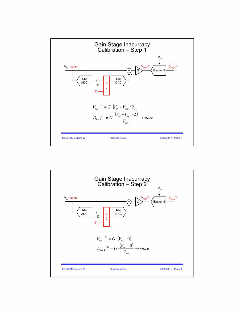
Accuracy Bootstrapping
• Highest sensitivity to gain errors in front-end stages
∏∏−
=
−
−−
=
− +⎟⎟⎠
⎞⎜⎜⎝
⎛−++⎟⎟
⎠
⎞⎜⎜⎝
⎛−+⎟⎟
⎠
⎞⎜⎜⎝
⎛−+= 1
1
)1(
)1(2
1
)1(
2
2
1
2
1
11, 1...11 n
jdj
qn
nd
nn
jdj
nq
dd
q
dqADCinout
GGG
GGG
GGGVD
εεεε
ΣΣ
εq1
- G1
Σ
ΣΣ
εq2
- G2
Σ
ΣΣ
εq(n-1)
- Gn-1
Σ
Vin,ADC
Dout 1/Gd1 1/Gd2
Vres1 Vres2 Vres(n-1)
Σ
1/Gd(n-1)
εqnD1 D2 D(n-1)Dn
EECS 247 Lecture 23 Pipelined ADCs © 2008 H.K. Page 11
"Accuracy Bootstrapping"
VinBn bitsStage 3Stage 2Stage 1 Stage k
“Sufficiently Accurate“Direction of Calibration
Ref:
A. N. Karanicolas et al. "A 15-b 1-Msample/s digitally self-calibrated pipeline ADC," IEEE J. Of Solid-State Circuits, pp. 1207-15, Dec. 1993
E. G. Soenen et al., "An architecture and an algorithm for fully digital correction of monolithic pipelined ADCs," TCAS II, pp. 143-153, March 1995
L. Singer et al., "A 12 b 65 MSample/s CMOS ADC with 82 dB SFDR at 120 MHz," ISSCC 2000, Digest of Tech. Papers., pp. 38-9 (calibration in opposite direction!)
EECS 247 Lecture 23 Pipelined ADCs © 2008 H.K. Page 12
Pipeline ADCErrors
• Non-idealities associated with sub-ADCs, sub-DACs and gain stages error in overall pipeline ADC performance
• Need to find means to tolerate/correct errors
• Important sources of error– Sub-ADC errors- comparator offset– Gain stage offset– Gain stage error– Sub-DAC error

EECS 247 Lecture 23 Pipelined ADCs © 2008 H.K. Page 13
DAC Errors
• Can be corrected digitally as well• Same calibration concept as gain errors
Vary DAC codes & measure errors via backend ADC
Vin +-
B1-bitDAC
D
GVres1
Dback
B1-bitADC +
Dout - 1/G
εDAC
+
Backend
EECS 247 Lecture 23 Pipelined ADCs © 2008 H.K. Page 14
DAC Calibration – Step 1
• εDAC(0) equivalent to offset - ignore
+-
B1-bitDAC
D
GVres1
Dback
B1-bitADC +
Dout1/G
BackendVin= const.
MUX
“0“
+
εDAC (0)
EECS 247 Lecture 23 Pipelined ADCs © 2008 H.K. Page 15
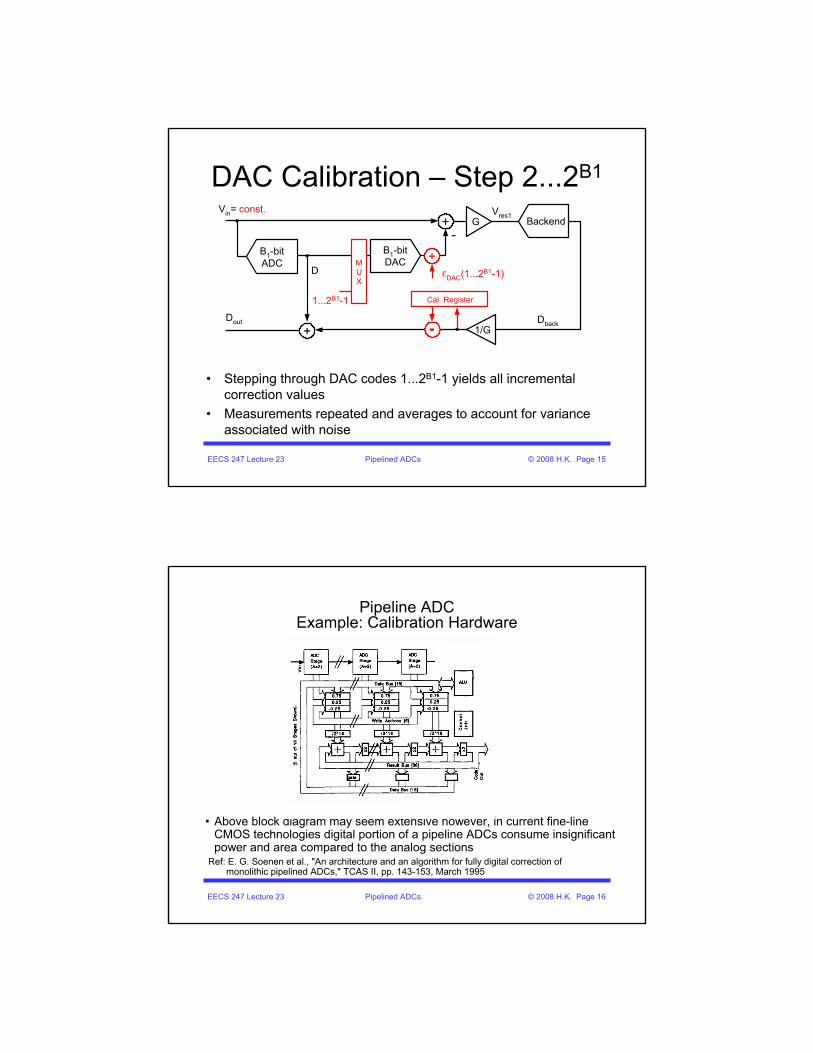
DAC Calibration – Step 2...2B1
• Stepping through DAC codes 1...2B1-1 yields all incremental correction values
• Measurements repeated and averages to account for variance associated with noise
+-
B1-bitDAC
D
GVres1
Dback
B1-bitADC +
Dout1/G
εDAC(1...2B1-1)
BackendVin= const.
MUX
1...2B1-1
+
Cal. Register
-
EECS 247 Lecture 23 Pipelined ADCs © 2008 H.K. Page 16
Pipeline ADC Example: Calibration Hardware
• Above block diagram may seem extensive however, in current fine-line CMOS technologies digital portion of a pipeline ADCs consume insignificant power and area compared to the analog sections
Ref: E. G. Soenen et al., "An architecture and an algorithm for fully digital correction of monolithic pipelined ADCs," TCAS II, pp. 143-153, March 1995

EECS 247 Lecture 23 Pipelined ADCs © 2008 H.K. Page 17
Pipelined ADC Error Correction/Calibration Summary
VIN1 VRES1
DAC
D1
-
a3V3
+23
ADC
+
VOS
+
+εADC
+εDAC
εgain
Either sufficient component matching or digital calibration
εDAC
?Inter-stage amplifier non-linearity
Digital adjustmentεgain
Redundancy either same stage or next stageεADC, Vos
Correction/CalibrationError
EECS 247 Lecture 23 Pipelined ADCs © 2008 H.K. Page 18
Inter-stage Gain Nonlinearity
Ref: B. Murmann and B. E. Boser, "A 12-b, 75MS/s Pipelined ADC using Open-Loop Residue Amplification," ISSCC Dig. Techn. Papers, pp. 328-329, 2003
• Invert gain stage non-linear polynomial• Express error as function of VRES1• Push error into digital domain through backend

EECS 247 Lecture 23 Pipelined ADCs © 2008 H.K. Page 19
Inter-stage Gain Nonlinearity
Ref: B. Murmann and B. E. Boser, "A 12-b, 75MS/s Pipelined ADC using Open-Loop Residue Amplification," ISSCC Dig. Techn. Papers, pp. 328-329, 2003
VRES1
a3VX3
+ BackendDB DB,corr
(...)
+-
...D12pD3pDp)p,(D 7B
32
5B
22
3B22B +−+−=ε
VX
ε(DB, p2)33
32
εgain )(2ap+
=
23
εgain
• Pre-computed table look-up•p2 continuously estimated & updated (account for temp. & other variations)
EECS 247 Lecture 23 Pipelined ADCs © 2008 H.K. Page 20
Inter-stage Gain Nonlinearity CompensationProof of Concept Evaluation Prototype
Ref: B. Murmann and B. E. Boser, "A 12-b, 75MS/s Pipelined ADC using Open-Loop Residue Amplification," ISSCC Dig. Techn. Papers, pp. 328-329, 2003
• Re-used 14-bit ADC in 0.35μm from Analog Devices [Kelly, ISSCC 2001]• Modified only 1st stage with 3-beff open-loop amplifier built with simple diff-pair +
resistive load instead of the conventional feedback around high-gain amp• Conventional 9-beff backend, 2-bit redundancy in 1st stage• Real-time post-processor off-chip (FPGA)
EECS 247 Lecture 23 Pipelined ADCs © 2008 H.K. Page 21
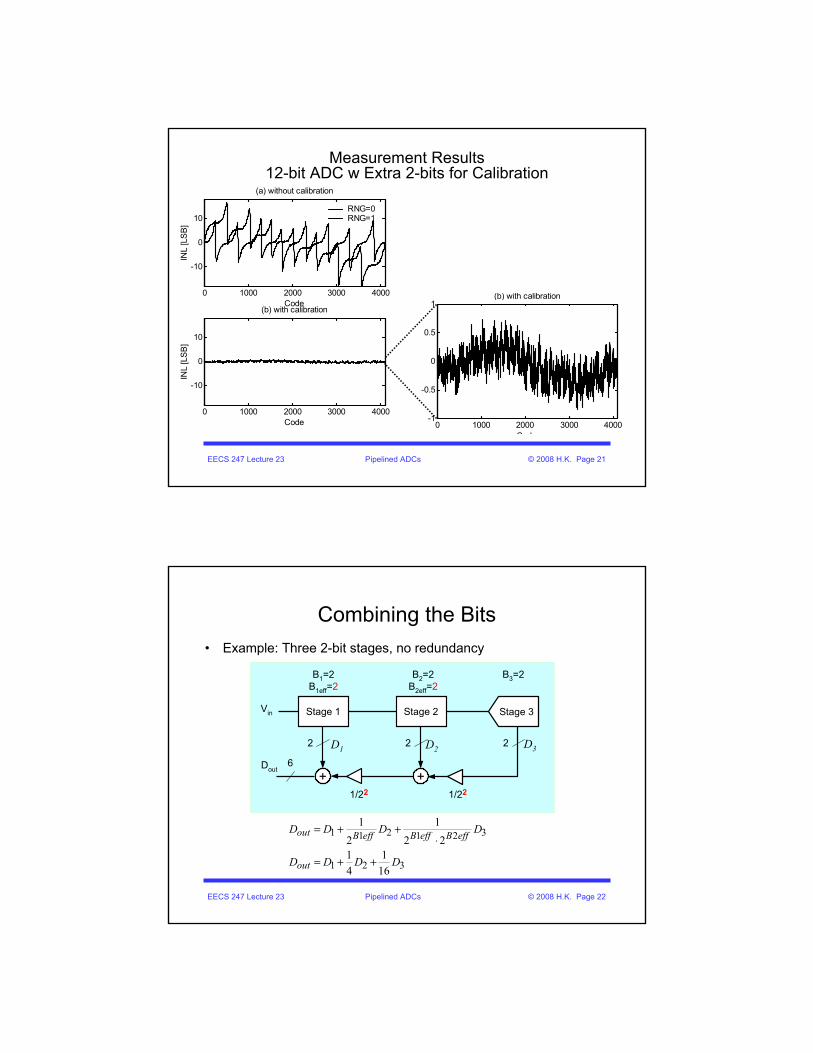
Measurement Results12-bit ADC w Extra 2-bits for Calibration
0 1000 2000 3000 4000-1
-0.5
0
0.5
1(b) with calibration
C d
0 1000 2000 3000 4000
-10
0
10
(a) without calibration
Code
INL
[LS
B]
RNG=0RNG=1
0 1000 2000 3000 4000
-10
0
10
(b) with calibration
Code
INL
[LSB
]
EECS 247 Lecture 23 Pipelined ADCs © 2008 H.K. Page 22
Combining the Bits• Example: Three 2-bit stages, no redundancy
Stage 2Vin Stage 3Stage 1
Dout+ +
2 2 2
6
B1=2B1eff=2
B2=2B2eff=2
B3=2
1/22 1/22
D1 D2 D3
321
321211
161
41
221
21
DDDD
DDDD
out
effBeffBeffBout
++=
⋅++=

EECS 247 Lecture 23 Pipelined ADCs © 2008 H.K. Page 23
Combining the Bits• Only bit shifts
• No arithmetic circuits needed
D1 XX D2 XX
D3 XX
------------
Dout DDDDDD
Stage 2Vin Stage 3Stage 1
Dout[5:0]
B1=2B1eff=2
B2=2B2eff=2
B3=2
MSB LSB
D1D2
D3
EECS 247 Lecture 23 Pipelined ADCs © 2008 H.K. Page 24
Combining the Bits Including Redundancy
• Example: Three 2-bit stages, incorporating 1- bit redundancy in stages 1 and 2
Stage 2Vin Stage 3Stage 1
B1=3B1eff=2
B2=3B2eff=2
B3=2
“8 Wires“
“6 Wires“
???
Dout[5:0]
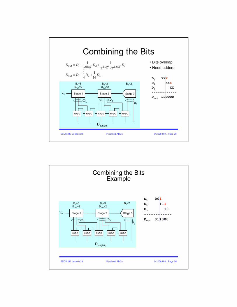
EECS 247 Lecture 23 Pipelined ADCs © 2008 H.K. Page 25
Combining the Bits• Bits overlap• Need adders
D1 XXX
D2 XXX
D3 XX
------------
Dout DDDDDDStage 2Vin Stage 3Stage 1
Dout[5:0]
B1=3B1eff=2
B2=3B2eff=2
B3=2
HADDHADDFADDHADDHADD
D1D2
D3
321
321211
161
41
221
21
DDDD
DDDD
out
effBeffBeffBout
++=
⋅++=
EECS 247 Lecture 23 Pipelined ADCs © 2008 H.K. Page 26
Combining the BitsExample
D1 001
D2 111
D3 10
------------Dout 011000
Stage 2Vin Stage 3Stage 1
Dout[5:0]
B1=3B1eff=2
B2=3B2eff=2
B3=2
HADDHADDFADDHADDHADD
D1D2
D3
EECS 247 Lecture 23 Pipelined ADCs © 2008 H.K. Page 27
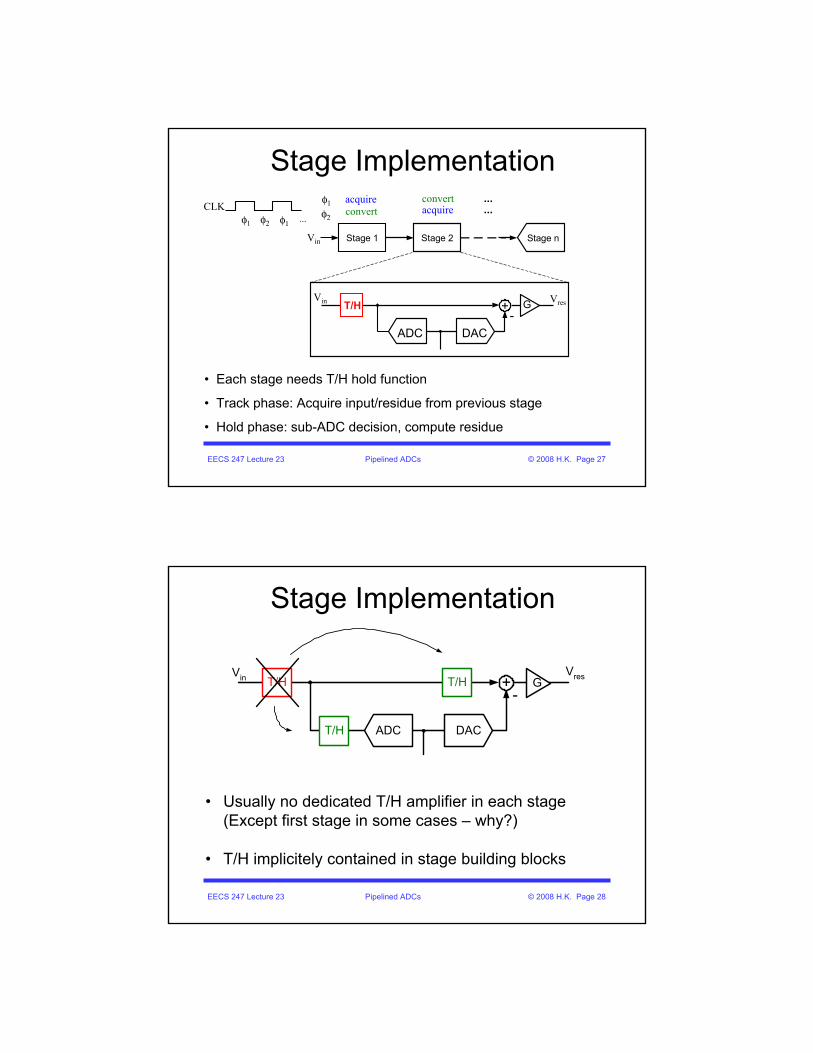
Stage Implementation
• Each stage needs T/H hold function
• Track phase: Acquire input/residue from previous stage
• Hold phase: sub-ADC decision, compute residue
Stage 1 Stage 2Vin Stage n
acquireconvert
convertacquire
...
...φ1 ...
CLK
+-
DACADC
G VresT/H
φ2 φ1
φ1φ2
Vin
EECS 247 Lecture 23 Pipelined ADCs © 2008 H.K. Page 28
Stage Implementation
• Usually no dedicated T/H amplifier in each stage (Except first stage in some cases – why?)
• T/H implicitely contained in stage building blocks
Vin +-
DACADC
GVresT/H T/H
T/H

EECS 247 Lecture 23 Pipelined ADCs © 2008 H.K. Page 29
Stage Implementation
• DAC-subtract-gain function can be lumped into a single switched capacitor circuit
• "MDAC"
Vin+
-
DACADC
GVresT/H
T/HMDAC
EECS 247 Lecture 23 Pipelined ADCs © 2008 H.K. Page 30
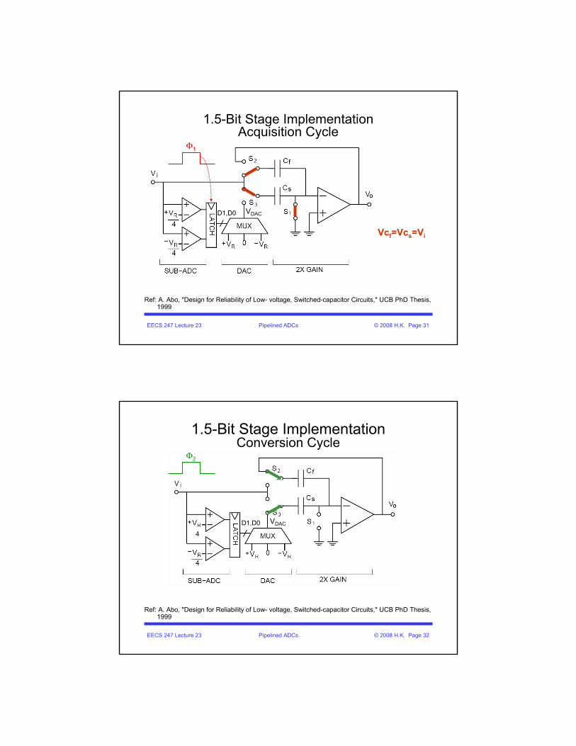
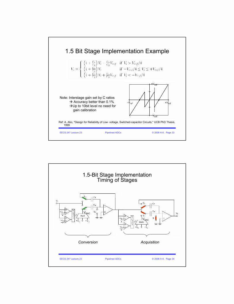
1.5-Bit Stage Implementation Example
Ref: A. Abo, "Design for Reliability of Low- voltage, Switched-capacitor Circuits," UCB PhD Thesis, 1999
D1,D0 VDAC
EECS 247 Lecture 23 Pipelined ADCs © 2008 H.K. Page 31
1.5-Bit Stage ImplementationAcquisition Cycle
Ref: A. Abo, "Design for Reliability of Low- voltage, Switched-capacitor Circuits," UCB PhD Thesis, 1999
D1,D0 VDAC
Vcf=Vcs=Vi
Φ1
EECS 247 Lecture 23 Pipelined ADCs © 2008 H.K. Page 32
1.5-Bit Stage ImplementationConversion Cycle
Ref: A. Abo, "Design for Reliability of Low- voltage, Switched-capacitor Circuits," UCB PhD Thesis, 1999
D1,D0 VDAC
Φ2
EECS 247 Lecture 23 Pipelined ADCs © 2008 H.K. Page 33
1.5 Bit Stage Implementation Example
Ref: A. Abo, "Design for Reliability of Low- voltage, Switched-capacitor Circuits," UCB PhD Thesis, 1999
Note: Interstage gain set by C ratiosAccuracy better than 0.1%Up to 10bit level no need forgain calibration
EECS 247 Lecture 23 Pipelined ADCs © 2008 H.K. Page 34
1.5-Bit Stage ImplementationTiming of Stages
VDAC
VDAC
Conversion Acquisition

EECS 247 Lecture 23 Pipelined ADCs © 2008 H.K. Page 35
Pipelined ADC Stage Power Dissipation & Noise• Typically pipeline ADC noise dominated by inter- stage gain blocks• Sub-ADC comparator noise translates into comparator threshold
uncertainty and is compensated for by redundancy
Vin Stage 1 Stage 3Stage 2
Vn2 Vn3Vn1
G1 G2 G3Vin
2 2in 2 n2 n3noise n1 2 2 2
V VV V .. .
G1 G1 G2= + + +
EECS 247 Lecture 23 Pipelined ADCs © 2008 H.K. Page 36
Pipelined ADC Stage Scaling• Example: Pipeline using 1-biteff stages
• Total input referred noise power:
C1/2
C1
Gm
C2/2
C2
Gm
C3/2
C3
GmVin
Vn2 Vn3Vn1
G1=2 G2=2 G3=2Vin
tot 2 2 21 2 3
tot1 2 3
1 1 1N kT .. .
C G1 C G1 G2 C1 1 1
N kT . . .C 4C 16C
⎡ ⎤∝ + + +⎢ ⎥
⎢ ⎥⎣ ⎦⎡ ⎤
∝ + + +⎢ ⎥⎢ ⎥⎣ ⎦

EECS 247 Lecture 23 Pipelined ADCs © 2008 H.K. Page 37
C1/2
C1
Gm
C2/2
C2
Gm
C3/2
C3
GmVin
• If all caps made the same size, backend stages contribute very little noise
• Wasteful power-wise, because:Power ~ Gm
Speed ~ Gm/CFixed speed Gm/C filxed Power ~ C
⎥⎦
⎤⎢⎣
⎡+++∝ ...
161
411
321 CCCkTNtot
Pipelined ADC Stage Scaling
EECS 247 Lecture 23 Pipelined ADCs © 2008 H.K. Page 38
• How about scaling caps down by G2=22=4x per stage?– Same amount of noise from every stage– All stages contribute significant noise– To keep overall noise the same noise/stage must be
reduced– Power ~ Gm ~ C goes up!
C1/2
C1
Gm
C2/2
C2
Gm
C3/2
C3
GmVin
⎥⎦
⎤⎢⎣
⎡+++∝ ...
161
411
321 CCCkTNtot
Pipelined ADC Stage Scaling

EECS 247 Lecture 23 Pipelined ADCs © 2008 H.K. Page 39
Stage ScalingExample: 2-biteff /stage
• Optimum capacitior scaling lies approximately midway between these two extremes
Ref: D. W. Cline, P.R. Gray "A power optimized 13-b 5MSamples/s pipelined analog-to-digital converter in 1.2um CMOS," JSSC 3/1996
EECS 247 Lecture 23 Pipelined ADCs © 2008 H.K. Page 40
Pipeline ADCStage Scaling
• Power minimum is "shallow“
• Near optimum solution in practice: Scale capacitors by stage gain
• E.g. for effective stage resolution of 1bit (Gain=2):
C/2
CGm
C/4
C/2Gm
C/8
C/4GmVin

EECS 247 Lecture 23 Pipelined ADCs © 2008 H.K. Page 41
Stage Scaling Example
Ref: D. W. Cline, P.R Gray "A power optimized 13-b 5 MSamples/s pipelined analog-to-digital converter in 1.2um CMOS," JSSC 3/1996
Note:Resolution per stage:
2bits A=4
EECS 247 Lecture 23 Pipelined ADCs © 2008 H.K. Page 42
How Many Bits Per Stage?• Many possible architectures
– E.g. B1eff=3, B2eff=1, ...vs. B1eff=1, B2eff=1, B3eff=1, ...
• Complex optimization problem, fortunately optimum tends to beshallow...
• Qualitative answer:– Maximum speed for given technology
• Use small resolution-per-stage (large feedback factor)– Maximum power efficiency for fixed, "low" speed
• Try higher resolution stages• Can help alleviate matching & noise requirements in stages
following the 1st stageRef: Singer VLSI 96, Yang, JSSC 12/01

EECS 247 Lecture 23 Pipelined ADCs © 2008 H.K. Page 43
14 & 12-Bit State-of-the-Art Implementations
260mW340mWPower
80MS/s75MS/sSpeed
~66dB/75dB~73dB/88dBSNR/SFDR
1-1-1-1-1-1-1-1-1-1-23-1-1-1-1-1-1-1-1-3Architecture
1214Bits
Loloee(ESSIRC 2002)
0.18μ/3V
Yang(JSSC 12/2001)
0.35μ/3V
Reference
EECS 247 Lecture 23 Pipelined ADCs © 2008 H.K. Page 44
10 & 8-Bit State-of-the-Art Implementations
30mW40mWPower
200MS/s125MS/sSpeed
~48dB/56dB~55dB/66dBSNR/SFDR
2.8 -2.8 - 41.5bit/stageArchitecture
810Bits
Kim et al(ISSCC 2005)
0.18μ/1.8V
Yoshioko et al(ISSCC 2005)
0.18μ/1.8V
Reference
EECS 247 Lecture 23 Pipelined ADCs © 2008 H.K. Page 45
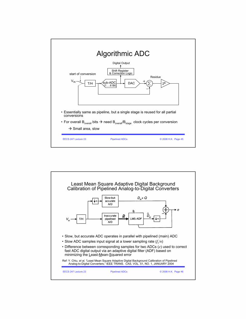
Algorithmic ADC
• Essentially same as pipeline, but a single stage is reused for all partial conversions
• For overall Boverall bits need Boverall/Bstage clock cycles per conversion
Small area, slow
T/H sub-ADC(1….6 Bit)
Digital Output
VIN
Residue
DAC
Shift Register& Correction Logicstart of conversion
2B
EECS 247 Lecture 23 Pipelined ADCs © 2008 H.K. Page 46
Least Mean Square Adaptive Digital Background Calibration of Pipelined Analog-to-Digital Converters
Ref: Y. Chiu, et al, “Least Mean Square Adaptive Digital Background Calibration of Pipelined Analog-to-Digital Converters,“ IEEE TRANS. CAS, VOL. 51, NO. 1, JANUARY 2004
• Slow, but accurate ADC operates in parallel with pipelined (main) ADC• Slow ADC samples input signal at a lower sampling rate (fs/n)• Difference between corresponding samples for two ADCs (e) used to correct
fast ADC digital output via an adaptive digital filter (ADF) based on minimizing the Least-Mean-Squared error

EECS 247 Lecture 23 Pipelined ADCs © 2008 H.K. Page 47
Example: "A 12-bit 20-MS/s pipelined analog-to-digital converter with nested digital background calibration"
Ref: X. Wang, P. J. Hurst, S. H. Lewis, " A 12-bit 20-Msample/s pipelined analog-to-digital converter with nested digital background calibration”, IEEE JSSC, vol. 39, pp. 1799 - 1808, Nov. 2004
• Pipelined ADC operates at 20Ms/s @ has 1.5bit/stage• Slow ADC Algorithmic type operating at 20Ms/32=625ks/s• Digital correction accounts for bit redundancy• Digital error estimator minimizes the mean-squared-error
EECS 247 Lecture 23 Pipelined ADCs © 2008 H.K. Page 48
Algorithmic ADC Used for Calibration of Pipelined ADC (continued from previous page)
Ref: X. Wang, P. J. Hurst, S. H. Lewis, " A 12-bit 20-MS/s pipelined analog-to-digital converter with nested digital background calibration”, IEEE JSSC, vol. 39, pp. 1799 - 1808, Nov. 2004
• Uses replica of pipelined ADC stage • Requires extra SHA in front to hold residue• Undergoes a calibration cycle periodically prior to being used to calibrate
pipelined ADC

EECS 247 Lecture 23 Pipelined ADCs © 2008 H.K. Page 49
12-bit 20-MS/s Pipelined ADC with Digital Background Calibration
Ref: X. Wang, P. J. Hurst, S. H. Lewis, " A 12-bit 20-MS/s pipelined analog-to-digital converter with nested digital background calibration”, IEEE JSSC, vol. 39, pp. 1799 - 1808, Nov. 2004
Sampling capacitors scaled:• Input SHA: 6pF• Pipelined ADC: 2pF,0.9,0.4,0.2, 0.1,0.1…• Algorithmic ADC: 0.2pF
Chip area: 13.2mm2
• Area of Algorithmic ADC <20%• Does not include digital
calibration circuitry estimated ~1.7mm2
EECS 247 Lecture 23 Pipelined ADCs © 2008 H.K. Page 50
Ref: X. Wang, P. J. Hurst, S. H. Lewis, " A 12-bit 20-MS/s pipelined analog-to-digital converter with nested digital background calibration”, IEEE JSSC, vol. 39, pp. 1799 - 1808, Nov. 2004
Without Calibration
|INL|<4.2LSB
WithCalibration
|INL|<0.5LSB
Measurement Results12-bit 20-MS/s Pipelined ADC with Digital Background Calibration

EECS 247 Lecture 23 Pipelined ADCs © 2008 H.K. Page 51
Ref: X. Wang, P. J. Hurst, S. H. Lewis, " A 12-bit 20-MS/s pipelined analog-to-digital converter with nested digital background calibration”, IEEE JSSC, vol. 39, pp. 1799 - 1808, Nov. 2004
Measurement Results12-bit 20-MS/s Pipelined ADC with Digital Background Calibration
Nyquist rate
EECS 247 Lecture 23 Pipelined ADCs © 2008 H.K. Page 52
Ref: X. Wang, P. J. Hurst, S. H. Lewis, " A 12-bit 20-MS/s pipelined analog-to-digital converter with nested digital background calibration”, IEEE JSSC, vol. 39, pp. 1799 - 1808, Nov. 2004
Measurement Results12-bit 20-MS/s Pipelined ADC with Digital Background Calibration
Does not include digital calibration circuitry estimated ~1.7mm2
Alg. ADC SNDR dominated by noise