Embed Size (px)
Citation preview

EE141
1
EE141EE141--Spring 2008Spring 2008Digital Integrated Digital Integrated CircuitsCircuitsCircuitsCircuits
Lecture 4Lecture 4
EE141EECS141 1Lecture #4
Manufacturing Process Manufacturing Process –– Design RulesDesign Rules
Administrative StuffAdministrative StuffLabs start next week
Pick one lab and stick to it
If Homework #1 not yet completedIf Homework #1 not yet completed, make sure you are aware of correction!Homework #2 out today, due next Fr.
EE141EECS141 2Lecture #4

EE141
2
ISSCC 2008ISSCC 2008
EE141EECS141 3Lecture #4
Class MaterialClass MaterialLast lecture
Brief introduction to CMOS inverter operationCMOS manufacturing process (intro)
Today’s lectureDesign rules (Ch. 2.3)
EE141EECS141 4Lecture #4
MOS Transistor ModelReading (2.3, 3.3.1-3.3.2)

EE141
3
oxidation
opticalmask
Review: PhotoReview: Photo--Lithographic ProcessLithographic Process
photoresist coatingphotoresistremoval (ashing)
photoresist
stepper exposure
development
Typical operations in a single photolithographic cycle (from [Fullman]).
EE141EECS141 5Lecture #4
processstep spin, rinse, dry
acid etch
development
Patterning of SiOPatterning of SiO22
Si-substrate
(a) Silicon base materialSiO2
Si-substrate
Hardened resist
Chemical or plasmaetch
(b) After oxidation and depositionof negative photoresist
PhotoresistSiO2
UV-lightPatternedoptical mask
Si-substrate
Si substrate
Si-substrate
SiO2
(d) After development and etching of resist,chemical or plasma etch of SiO2
(e) After etching
Hardened resist
EE141EECS141 6Lecture #4
Si-substrate Si-substrate
(c) Stepper exposure
Exposed resist SiO2
(f) Final result after removal of resist

EE141
4
Advanced MetallizationAdvanced Metallization
EE141EECS141 7Lecture #4
A Modern CMOS ProcessA Modern CMOS Processgate-oxide
p-well n-well
p-epi
SiO2
AlCu
poly
n+
SiO2
p+
Tungsten
TiSi2
EE141EECS141 8Lecture #4
p+
DualDual--Well ShallowWell Shallow--TrenchTrench--Isolated CMOS ProcessIsolated CMOS Process

EE141
5
Transistor LayoutTransistor Layout
SiO2Cross Sectional View
p-well SiO2
poly
n+
Cross-Sectional View
poly
EE141EECS141 9Lecture #4
Layout View
p-well
CMOS Process LayersCMOS Process LayersLayer
Well (p n)
Color Representation
Y ll
Polysilicon
Metal1
Metal2
Well (p,n)
Active Area (n+,p+)Yellow
Green
RedBlue
Magenta
Well contact (p+,n+) Green
EE141EECS141 10Lecture #4
Contact To Poly
Contact To Diffusion
Via
Black
BlackBlack

EE141
6
Layers in 0.25 Layers in 0.25 μμm CMOS processm CMOS process
EE141EECS141 11Lecture #4
(well contacts)
Design RulesDesign Rules
Interface between designer and processInterface between designer and process engineerGuidelines for constructing process masksUnit dimension: Minimum line width
scalable design rules: lambda parameter
EE141EECS141 12Lecture #4
absolute dimensions (micron rules)

EE141
7
Design RulesDesign RulesIntra-layer
Widths, spacing, areaInter-layer
Enclosures, distances, extensions, overlaps
S i l l ( b 0 25 )
EE141EECS141 13Lecture #4
Special rules (sub-0.25µm)Antenna rules, density rules, (area)
IntraIntra--Layer Design RulesLayer Design Rules9
02
Different PotentialSame Potential
4
10
0 Well
Active3
3
Polysilicon
2
Metal1 3
32
Contactor Via
2
or6
2Hole
EE141EECS141 14Lecture #4
Metal2 4
3
2Select
2

EE141
8
InterInter--Layer: Transistor LayoutLayer: Transistor Layout
or1
23
Tran
sist
o
EE141EECS141 15Lecture #4
5
InterInter--Layer: Vias and ContactsLayer: Vias and Contacts2
4
1
1
Via
Metal toPoly ContactMetal to
Active Contact
15
4
3 2
EE141EECS141 16Lecture #4
22

EE141
9
InterInter--Layer: Well and SubstrateLayer: Well and Substrate2
2
Select3
1
3 3
2 5
EE141EECS141 17Lecture #4
WellSubstrate
CMOS Inverter LayoutCMOS Inverter Layout
A A’
InGND VDD
A A’
Out
(a) Layout
EE141EECS141 18Lecture #4
np-substrate Field
Oxidep+n+
(b) Cross-Section along A-A’
A A’

EE141
10
Layout EditorLayout Editor
EE141EECS141 19Lecture #4
Design Rule CheckerDesign Rule Checker
EE141EECS141 20Lecture #4

EE141
11
Sticks DiagramSticks Diagram
3VDD
1
3
In Out • Dimensionless layout entities• Only topology is important
EE141EECS141 21Lecture #4
1GND
Stick diagram of inverter
Circuit Under DesignCircuit Under DesignVDD VDD
Vin Vout
M1
M2
M3
M4
Vout2
EE141EECS141 22Lecture #4
M1 M3

EE141
12
CMOS InverterCMOS InverterVDD
PMOS 2λVDD
N Well
Polysilicon
In Out
2λ
Metal 1
OutIn
PMOS
NMOS
Contacts
EE141EECS141 23Lecture #4
GNDNMOS
NMOS
Two InvertersTwo InvertersShare power and ground
A
Connect in Metal
Abut cells
VDD
EE141EECS141 24Lecture #4

EE141
13
MOS Transistor MOS Transistor ModelModel
EE141EECS141 25Lecture #4
Review: What is a Transistor?Review: What is a Transistor?
A MOS T i A S i h!
|VGS|
A MOS Transistor
|VGS| ≥ |VT|
S DRon
A Switch!
S D
G
EE141EECS141 26Lecture #4
S DS D

EE141
14
Switch Model of MOS TransistorSwitch Model of MOS Transistor
|V |G
|VGS|
S D
Ron
EE141EECS141 27Lecture #4
|VGS| < |VT| |VGS| > |VT|S D S D
DSGVGS
+
–
Threshold Voltage: ConceptThreshold Voltage: Concept
n+
p-substrate
B
Depletionregion
n-channel
n+
EE141EECS141 28Lecture #4
BWith positive gate bias, electrons pulled toward the gateWith large enough bias, enough electrons will be pulled to "invert" the surface (p→n type)Voltage at which surface inverts: “magic” threshold voltage VT

EE141
15
The Threshold VoltageThe Threshold Voltage
( )FSBFTT VVV φ−+φ⋅γ+= 220
Threshold
( )FSBFTT VVV φ−+φ⋅γ+= 220
i
ATF n
Nln⋅φ=φ
Fermi potential
EE141EECS141 29Lecture #4
2ΦF is approximately −0.6V for p-type substratesγ is the body factorVT0 is approximately 0.4 for our process
The Body EffectThe Body Effect
0.8
0.85
0.9
0.55
0.6
0.65
0.7
0.75
VT (V
)
EE141EECS141 30Lecture #4
-2.5 -2 -1.5 -1 -0.5 00.4
0.45
0.5
VBS
(V)
VT0
reverse body bias
EE141
16
SVGS VDS
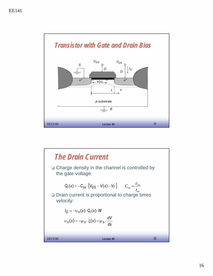
Transistor with Gate and Drain BiasTransistor with Gate and Drain Bias
n+n+
D
SG
xL
V(x) +–
ID
EE141EECS141 31Lecture #4
p-substrate
B
The Drain CurrentThe Drain CurrentCharge density in the channel is controlled by the gate voltage:
[ ]TGSoxi VxVVCxQ −−⋅−= )()(ox
oxox t
C ε=
Drain current is proportional to charge times velocity:
WxQxI iD ⋅⋅υ−= )()(
EE141EECS141 32Lecture #4
WxQxI inD ⋅⋅υ−= )()(
dxdVxx nnn ⋅μ=ξ⋅μ−=υ )()(

EE141
17
The Drain CurrentThe Drain Current
[ ]( )
( ) ( )D n iI W x Q xυ= ⋅ ⋅
Combining velocity and charge:
( )( )D n ox GS TI W C V V x V dV dxμ= ⋅ ⋅ ⋅ − − ⋅
Integrating over the channel:
( )⎥⎥⎦
⎤
⎢⎢⎣
⎡−⋅−⋅⋅=
2
2DS
DSTGSnDV
VVVL
WkI ’
EE141EECS141 33Lecture #4
ox
oxnoxnn t
Ck ε⋅μ=⋅μ= ’
Plot of IPlot of I--V CurveV Curve
EE141EECS141 34Lecture #4
Is this really what happens?

EE141
18
Does it really work this way?Does it really work this way?Why does the current bend down?
When (VGS-VTH)-VDS is negative, in our analysis the sign of the carriers changes
But transistors don’t actually behave this way
EE141EECS141 35Lecture #4
Look at what really happens to channel charge:
VGS
Transistor in SaturationTransistor in Saturation0< VGS - VT < VDS
n+n+
S
G
D
VDS > VGS - VT
VGS - VT+-
EE141EECS141 36Lecture #436
Pinch-off

EE141
19
SaturationSaturationFor (VGS – VT) < VDS, the effective drain voltage and current saturate:
( )22 TGSn
D VVL
WkI −⋅⋅=’
Real drain current isn’t totally independent of VDSFor example, approx. for channel-length modulation:
( ),DS eff GS TV V V= −
EE141EECS141 37Lecture #4
( ) ( )DSTGSn
D VVVL
WkI ⋅λ+⋅−⋅⋅= 12
2’
Modes of OperationModes of OperationCutoff:
VGS -VT< 0 0=DI
Linear (Resistive):VGS-VT > VDS ( )
⎥⎥⎦
⎤
⎢⎢⎣
⎡−⋅−⋅⋅=
2
2DS
DSTGSnDV
VVVL
WkI ’
EE141EECS141 38Lecture #4
Saturation:0 < VGS-VT < VDS ( )2
2 TGSn
D VVL
WkI −⋅⋅=’

EE141
20
6x 10
-4
VGS= 2.5 V
CurrentCurrent--Voltage Relations:Voltage Relations:A Good Ol’ TransistorA Good Ol’ Transistor
QuadraticRelationship
2
3
4
5
VGS= 2.0 V
V = 1 5 V
Resistive Saturation
VDS = VGS - VTI D(A
)
EE141EECS141 39Lecture #4
0 0.5 1 1.5 2 2.50
1
VGS= 1.5 V
VGS= 1.0 V
VDS (V)
A Model for Manual AnalysisA Model for Manual Analysis
( ) ( )DSTGSn
D VVVL
WkI ⋅λ+⋅−⋅⋅= 12
2’VDS > VGS – VT Saturation:
S
DG
ID
( )⎥⎥⎦
⎤
⎢⎢⎣
⎡−⋅−⋅⋅=
2
2DS
DSTGSnDV
VVVL
WkI ’
( ) ( )DSTGSD L2
VDS < VGS – VT Linear:
EE141EECS141 40Lecture #4
S ⎦⎣
( )FSBFTT VVV φ−+φ⋅γ+= 220
with