Embed Size (px)
Citation preview

EE141
1
EE1411
EECS141
EE141EE141--Fall 2006Fall 2006Digital Integrated Digital Integrated CircuitsCircuits
Lecture 23Lecture 23Sequential LogicSequential LogicTimingTiming
EE1412
EECS141
AnnouncementsAnnouncementsHomework 8 due on ThursdayProject phase three in lab this week
Project reports due on MondayPoster presentations next week

EE141
2
EE1413
EECS141
EE1414
EECS141

EE141
3
EE1415
EECS141
Class MaterialClass Material
Last lectureLatches and registers
Today’s lectureFinish sequential logicTiming
ReadingChapter 7, 10
EE1416
EECS141
Other Other Sequential Sequential CircuitsCircuits

EE141
4
EE1417
EECS141
Other Sequential CircuitsOther Sequential Circuits
Schmitt Trigger
Monostable Multivibrators
Astable Multivibrators
EE1418
EECS141
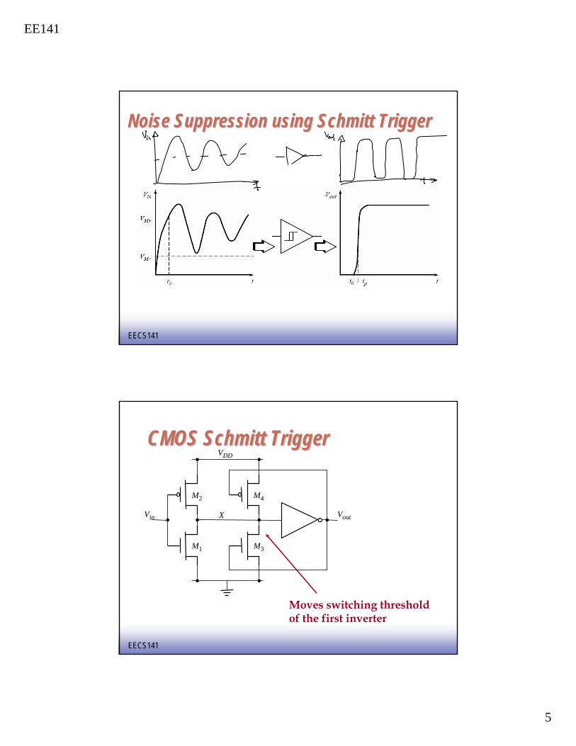
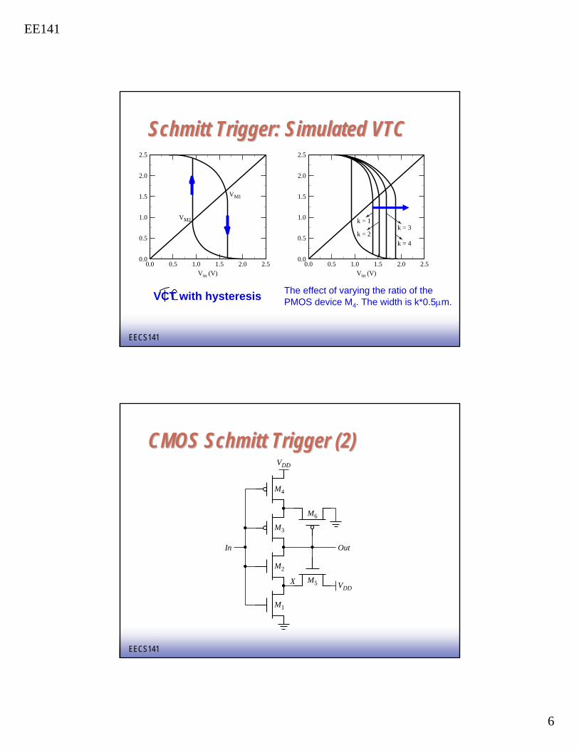
Schmitt TriggerSchmitt Trigger
In Out
Vin
Vout VOH
VOL
VM– VM+
•VTC with hysteresis
•Restores signal slopes
EE141
5
EE1419
EECS141
Noise Suppression using Schmitt TriggerNoise Suppression using Schmitt Trigger
EE14110
EECS141
CMOS Schmitt TriggerCMOS Schmitt Trigger
Moves switching thresholdof the first inverter
Vin
M2
M1
VDD
X Vout
M4
M3
EE141
6
EE14111
EECS141
2.5
V
X
(V)
VM2
VM1
Vin (V)
VCT with hysteresis
2.0
1.5
1.0
0.5
0.00.0 0.5 1.0 1.5 2.0 2.5
2.5
V
x
(V)
k = 2k = 3
k = 4
k = 1
Vin (V)
2.0
1.5
1.0
0.5
0.00.0 0.5 1.0 1.5 2.0 2.5
The effect of varying the ratio of the PMOS device M4. The width is k*0.5μm.
Schmitt Trigger: Simulated VTCSchmitt Trigger: Simulated VTC
EE14112
EECS141
CMOS Schmitt Trigger (2)CMOS Schmitt Trigger (2)
VDD
VDD
OutIn
M1
M5
M2
X
M3
M4
M6

EE141
7
EE14113
EECS141
Bistable Multivibrator
Monostable Multivibrator
Astable Multivibrator
flip-flop, Schmitt Trigger
one-shot
oscillator
S
R
T
MultivibratorMultivibrator CircuitsCircuits
EE14114
EECS141
DELAY
td
In
Outtd
TransitionTransition--Triggered MonostableTriggered Monostable
EE141
8
EE14115
EECS141
VDD
InOutA B
C
R
In
B
Out t
VM
t2t1
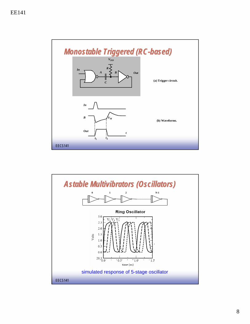
(a) Trigger circuit.
(b) Waveforms.
Monostable Triggered (RCMonostable Triggered (RC--based)based)
EE14116
EECS141
Astable Multivibrators (Oscillators)Astable Multivibrators (Oscillators)0 1 2 N-1
simulated response of 5-stage oscillator
EE141
9
EE14117
EECS141
Timing Timing DefinitionsDefinitions
EE14118
EECS141
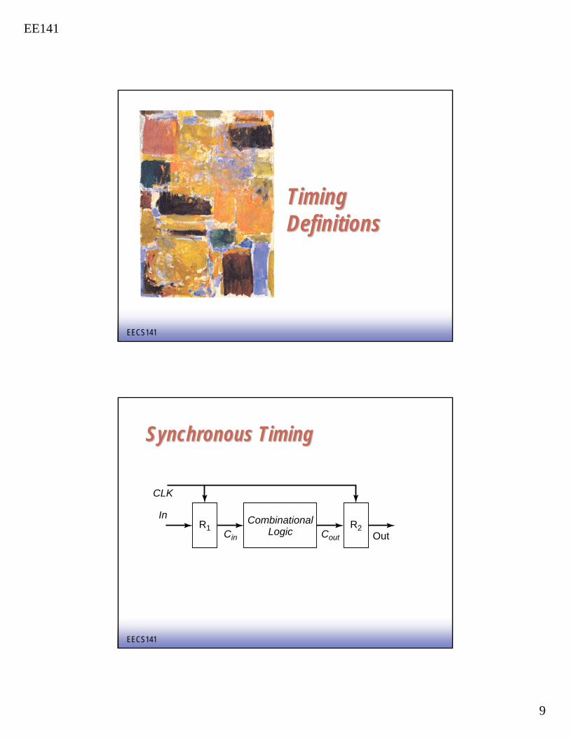
Synchronous TimingSynchronous Timing
CombinationalLogic
R1 R2Cin Cout Out
In
CLK

EE141
10
EE14119
EECS141
Latch ParametersLatch ParametersD
Clk
Q
D
Q
Clk
tc-q
thold
PWm tsu
td-q
Delays can be different for rising and falling data transitions
T
EE14120
EECS141
Register ParametersRegister ParametersD
Clk
Q
D
Q
Clk
tc-q
thold
T
tsu
Delays can be different for rising and falling data transitions

EE141
11
EE14121
EECS141
R1D Q Combinational
LogicIn
CLK tCLK1
R2D Q
tCLK2
tc − qtc − q, cdtsu, thold
tlogictlogic, cd
Cycle time: TClk > tc-q + tlogic + tsu
Race margin: thold < tc-q,cd + tlogic,cd
Timing Constraints Timing Constraints
EE14122
EECS141
Clock Clock NonidealitiesNonidealitiesClock skew
Spatial variation in temporally equivalent clock edges; deterministic + random, tSK
Clock jitterTemporal variations in consecutive edges of the clock signal; modulation + random noiseCycle-to-cycle (short-term) tJSLong term tJL
Variation of the pulse width Important for level sensitive clocking

EE141
12
EE14123
EECS141
Clock UncertaintiesClock Uncertainties
2
43
Power Supply
Interconnect
5 Temperature
6 Capacitive Load
7 Coupling to Adjacent Lines
1 Clock Generation
Devices
Sources of clock uncertainty
EE14124
EECS141
Clock Skew and JitterClock Skew and Jitter
Both skew and jitter affect the effective cycle timeOnly skew affects the race margin
Clk
Clk
tSK
tJS

EE141
13
EE14125
EECS141
Clock SkewClock Skew# of registers
Clk delayInsertion delayMax Clk skew
Earliest occurrenceof Clk edgeNominal – δ/2
Latest occurrenceof Clk edge
Nominal + δ /2
δ


