Embed Size (px)
Citation preview

EE1411
VLSI Test Principles and Architectures Chap. 11 - Analog and Mixed-Signal Testing - P.1
Chapter 11Chapter 11
Analog and Mixed-Signal TestingAnalog and Mixed-Signal Testing

EE1412
VLSI Test Principles and Architectures Chap. 11 - Analog and Mixed-Signal Testing - P.2
What is this chapter about?What is this chapter about?
Introduces AMS circuits, failure modes and fault models.
Addresses analog testing, including DC and AC parametric testing.
Discusses mixed-signal circuits, ADC and DAC, and their testing approaches.
Studies IEEE Std. 1149.4, the standard for mixed-signal test buses

EE1413
VLSI Test Principles and Architectures Chap. 11 - Analog and Mixed-Signal Testing - P.3
Chapter 11Chapter 11Analog and Mixed-Signal TestingAnalog and Mixed-Signal Testing
Introduction Analog Circuit Testing Mixed-Signal Testing IEEE Std. 1149.4 Standard for Mixed-
Signal Test Bus Concluding Remarks

EE1414
VLSI Test Principles and Architectures Chap. 11 - Analog and Mixed-Signal Testing - P.4
11.1 Introduction11.1 Introduction
Analog Circuit Properties Analog Defect Mechanism and Fault
Models

EE1415
VLSI Test Principles and Architectures Chap. 11 - Analog and Mixed-Signal Testing - P.5
Analog, Digital, and Mixed-Signal Signals Analog, Digital, and Mixed-Signal Signals
1
0
AnalogAnalog Mixed-SignalMixed-Signal DigitalDigital

EE1416
VLSI Test Principles and Architectures Chap. 11 - Analog and Mixed-Signal Testing - P.6
Analog Circuit PropertiesAnalog Circuit Properties Continuous Signal Large Range of Circuits Nonlinear Characteristics Feedback Ambiguity Complicated Cause-Effect Relationship Absence of Suitable Fault Model Accurate Measurements Required

EE1417
VLSI Test Principles and Architectures Chap. 11 - Analog and Mixed-Signal Testing - P.7
Properties - Properties - Continuous SignalContinuous Signal
• Logic 1, Logic 0• VIH, VIL, VOH, VOL• Rise Time, Fall Time• Propagation Delay H-L/L-H• Noise Margin High/Low
Digital Signal Analog Signal
• Voltage/Current• Slew Rate• Overshoot• Damping Factor• Frequency• Bandwidth
VH
VL
tLH tHL
SR
tSettle
VOV
VA

EE1418
VLSI Test Principles and Architectures Chap. 11 - Analog and Mixed-Signal Testing - P.8
Properties - Properties - Large Ranges of CircuitsLarge Ranges of Circuits
Digital Circuits Analog Circuits
•Operation •Static Logic•Dynamic Logic
•Structure•Gates•PLA•Memory
• Operation• Current Mode• Voltage Mode• Switching Cap
• Structure• Amplifier• Multiplier• Rectifier• Resonator

EE1419
VLSI Test Principles and Architectures Chap. 11 - Analog and Mixed-Signal Testing - P.9
Properties- Properties- Nonlinear CharacteristicsNonlinear Characteristics Analog circuits are nonlinear in nature
Nonlinear cause effect
DI
DV
2)(2
1tgsoxD VV
L
WCI TD VnV
sD eII /

EE14110
VLSI Test Principles and Architectures Chap. 11 - Analog and Mixed-Signal Testing - P.10
Properties- Properties- Feedback AmbiguitiesFeedback Ambiguities Feedback puts circuit parameters together Difficult to identify fault location
-
+
-
+
EE14111
VLSI Test Principles and Architectures Chap. 11 - Analog and Mixed-Signal Testing - P.11
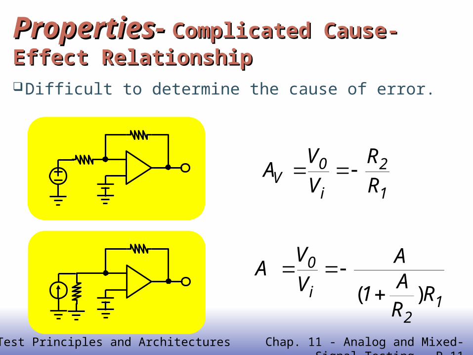
Properties- Properties- Complicated Cause-Effect RelationshipComplicated Cause-Effect Relationship
Difficult to determine the cause of error.
12
i
0
RRA
1
AV
VA
)(
1
2
i
0V R
R
V
VA

EE14112
VLSI Test Principles and Architectures Chap. 11 - Analog and Mixed-Signal Testing - P.12
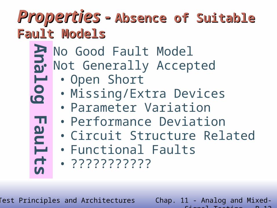
Properties – Properties – Absence of Suitable Fault Absence of Suitable Fault ModelsModels
Digital Faults
• Good Logic Fault Model• Generally Accepted
• Stuck-at-1, Stuck-at-0• Stuck-Open, Stuck-On• Short. Open• Memory Faults• PLA Faults
EE14113
VLSI Test Principles and Architectures Chap. 11 - Analog and Mixed-Signal Testing - P.13
Properties - Properties - Absence of Suitable Fault ModelsAbsence of Suitable Fault Models
An
alog
Fau
lts
• No Good Fault Model• Not Generally Accepted
• Open Short• Missing/Extra Devices• Parameter Variation• Performance Deviation• Circuit Structure Related• Functional Faults• ???????????

EE14114
VLSI Test Principles and Architectures Chap. 11 - Analog and Mixed-Signal Testing - P.14
PropertiesProperties – – Accurate Measurements RequiredAccurate Measurements Required
Digital Instrument
• Oscilloscope• Function Generator• Logic Analyzer• Frequency Counter

EE14115
VLSI Test Principles and Architectures Chap. 11 - Analog and Mixed-Signal Testing - P.15
An
alo
g In
stru
men
t• Oscilloscope• Function Gen• Freq. Counter• Spectrum Analyzer• Network Analyzer• Impedance Analyzer• Timing Analyzer• Communication Analyzer• RF Instrument• Optical Instrument• Microwave Instrument
Properties – Properties – Accurate Measurements RequiredAccurate Measurements Required

EE14116
VLSI Test Principles and Architectures Chap. 11 - Analog and Mixed-Signal Testing - P.16
11.1 Introduction11.1 Introduction
Analog Circuit Properties Analog Defect Mechanism and Fault
Models

EE14117
VLSI Test Principles and Architectures Chap. 11 - Analog and Mixed-Signal Testing - P.17
Defect Mechanisms (1)Defect Mechanisms (1) Material Defects
cracks crystal imperfection surface impurities ion migration
Processing Faults oxide thickness mobility change impurity density diffusion depth dielectric constants metal sheet resistance missing contacts dust

EE14118
VLSI Test Principles and Architectures Chap. 11 - Analog and Mixed-Signal Testing - P.18
Defect Mechanisms (2)Defect Mechanisms (2)
Time-Dependent Failures dielectric breakdown electron migration
Packaging Failures contact degradation seal leakage

EE14119
VLSI Test Principles and Architectures Chap. 11 - Analog and Mixed-Signal Testing - P.19
Analog Fault Model Analog Fault Model
Defects/Failure
Hard Faults Soft Faults
EE14120
VLSI Test Principles and Architectures Chap. 11 - Analog and Mixed-Signal Testing - P.20
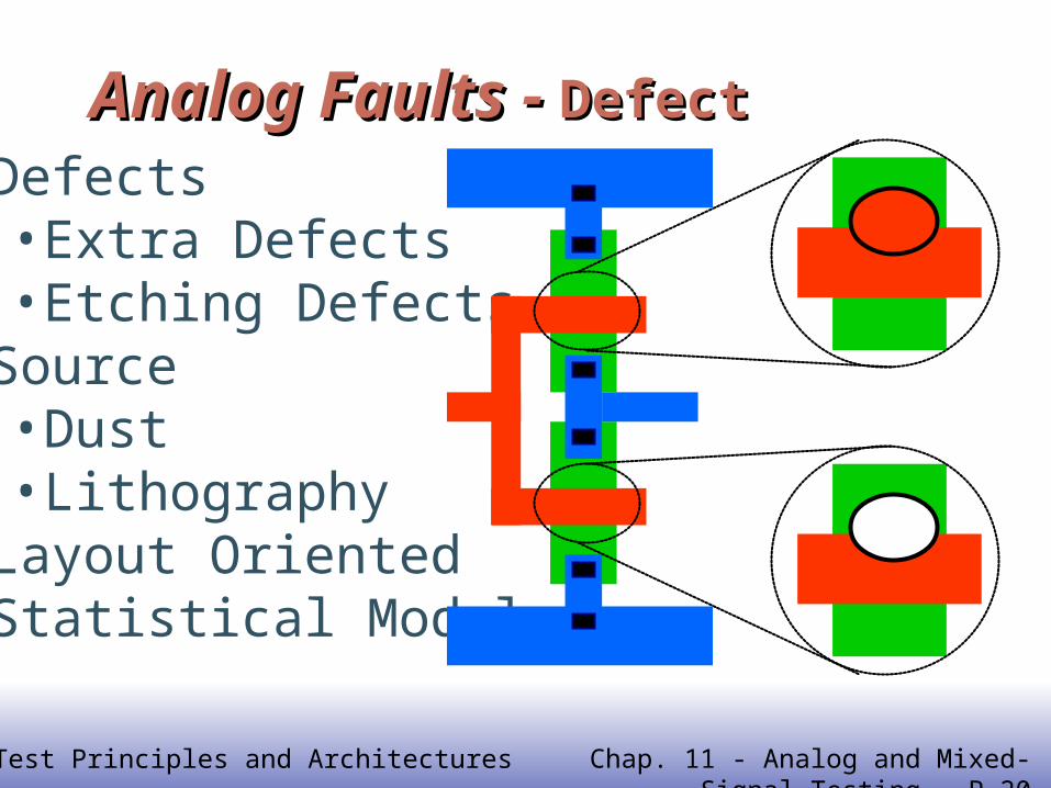
Analog Faults - Analog Faults - DefectDefect
• Defects• Extra Defects• Etching Defects
• Source• Dust• Lithography
• Layout Oriented• Statistical Model
EE14121
VLSI Test Principles and Architectures Chap. 11 - Analog and Mixed-Signal Testing - P.21
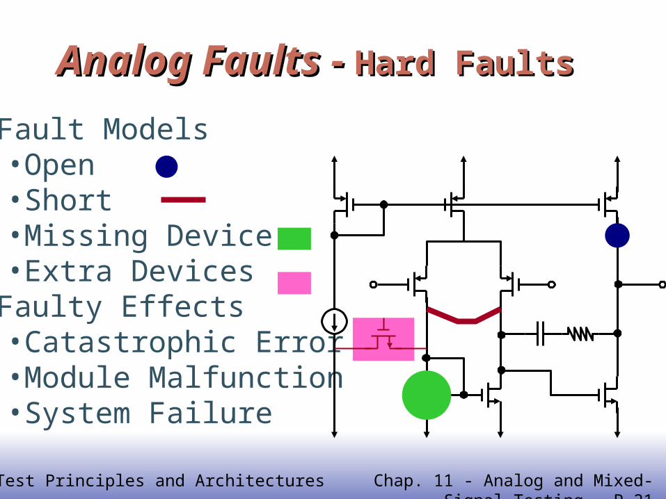
Analog Faults - Analog Faults - Hard FaultsHard Faults
•Fault Models•Open•Short•Missing Device•Extra Devices
•Faulty Effects•Catastrophic Error•Module Malfunction•System Failure

EE14122
VLSI Test Principles and Architectures Chap. 11 - Analog and Mixed-Signal Testing - P.22
Analog Faults - Analog Faults - Soft FaultsSoft Faults
• Parametric Faults• Io: 100uA -> 50uA• W: 20um -> 10um
• Deviation Faults• fo: 10MHz -> 5MHz• Gain: 10000 -> 2000
• Sources• Mobility• Oxide Thickness• Impurity Density• Defusion Depth• Dielectric Constants• Metal Sheet Resistance
EE14123
VLSI Test Principles and Architectures Chap. 11 - Analog and Mixed-Signal Testing - P.23
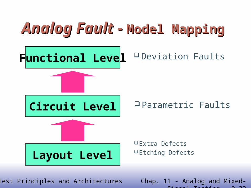
Analog Fault - Analog Fault - Model MappingModel Mapping
Deviation Faults
Parametric Faults
Functional Level
Circuit Level
Layout Level Extra Defects Etching Defects
EE14124
VLSI Test Principles and Architectures Chap. 11 - Analog and Mixed-Signal Testing - P.24
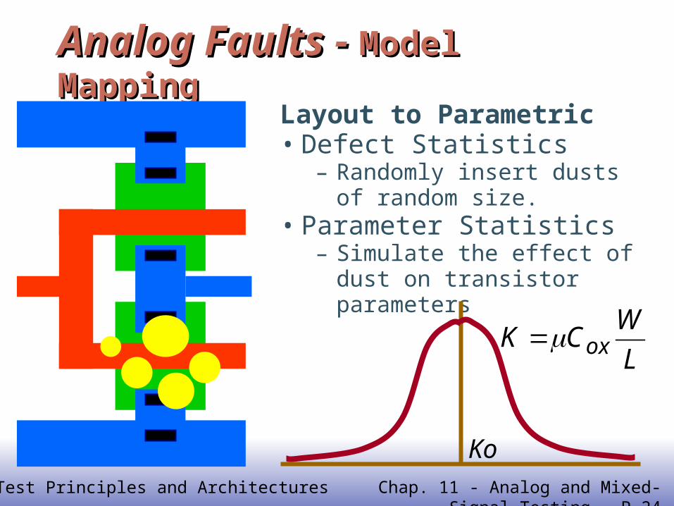
Analog Faults - Analog Faults - Model MappingModel Mapping
Layout to Parametric• Defect Statistics
– Randomly insert dusts of random size.
• Parameter Statistics– Simulate the effect of dust on
transistor parameters
L
WCK ox
Ko
EE14125
VLSI Test Principles and Architectures Chap. 11 - Analog and Mixed-Signal Testing - P.25
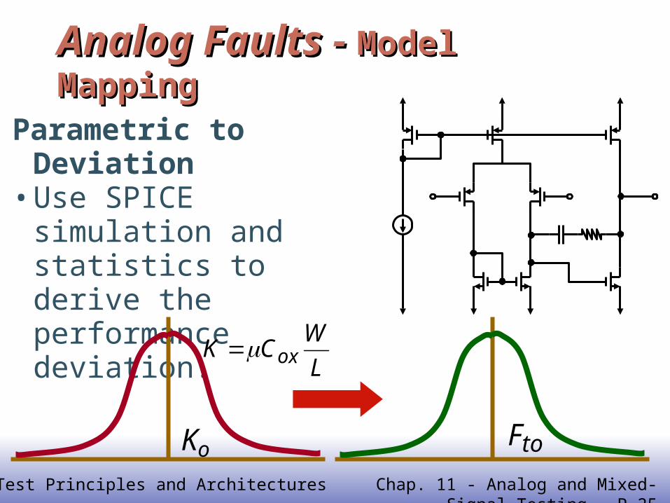
Analog Faults - Analog Faults - Model MappingModel Mapping
Parametric to Deviation• Use SPICE simulation
and statistics to derive the performance deviation.
L
WCK ox
Ko Fto
EE14126
VLSI Test Principles and Architectures Chap. 11 - Analog and Mixed-Signal Testing - P.26
Studied the analog test properties Nonlinearity, Feedback Ambiguity No good fault model
Overview the analog test plan Test Code, Binning, Sequence Control Focused Calibrations, DIB Checkers Characterization and Simulation Code
Analog Fault Model Extra and Etching Defects Parametric and Deviation faults Model Mapping
11.1 Summary11.1 Summary
EE14127
VLSI Test Principles and Architectures Chap. 11 - Analog and Mixed-Signal Testing - P.27
11.2 Analog Circuit Testing11.2 Analog Circuit Testing
Analog Test Approaches Analog Test Waveforms DC Parametric Testing AC Parametric Testing

EE14128
VLSI Test Principles and Architectures Chap. 11 - Analog and Mixed-Signal Testing - P.28
Analog Testing Analog Testing
Spec Oriented
WaveformOriented

EE14129
VLSI Test Principles and Architectures Chap. 11 - Analog and Mixed-Signal Testing - P.29
Specification Oriented TestSpecification Oriented Test
Analog Devices, Inc.TM

EE14130
VLSI Test Principles and Architectures Chap. 11 - Analog and Mixed-Signal Testing - P.30
Specification Oriented TestSpecification Oriented Test Specification Oriented Test
Check whether all the specs are metTedious and inflexible
Example: Operational AmplifierDC Specifications
–Input Offset Voltage–Input Bias Offset Current–Open-Loop Gain–Noise–Common Rejection Ratio–Temperature Drift
AC Specifications– Bandwidth– Harmonic Distortion– Slew Rate– Settling Time– Noise

EE14131
VLSI Test Principles and Architectures Chap. 11 - Analog and Mixed-Signal Testing - P.31
Waveform Oriented TestWaveform Oriented Test
Waveform Oriented Test Compare waveform to the simulated ones

EE14132
VLSI Test Principles and Architectures Chap. 11 - Analog and Mixed-Signal Testing - P.32
Waveform Oriented TestWaveform Oriented Test
A DC Bias, Input Offset
B Slew Rate, Damping Factor
C Overshoot, Damping Factor, Bandwidth
D Settling Time, DC Gain
A
B
C
D
EE14133
VLSI Test Principles and Architectures Chap. 11 - Analog and Mixed-Signal Testing - P.33
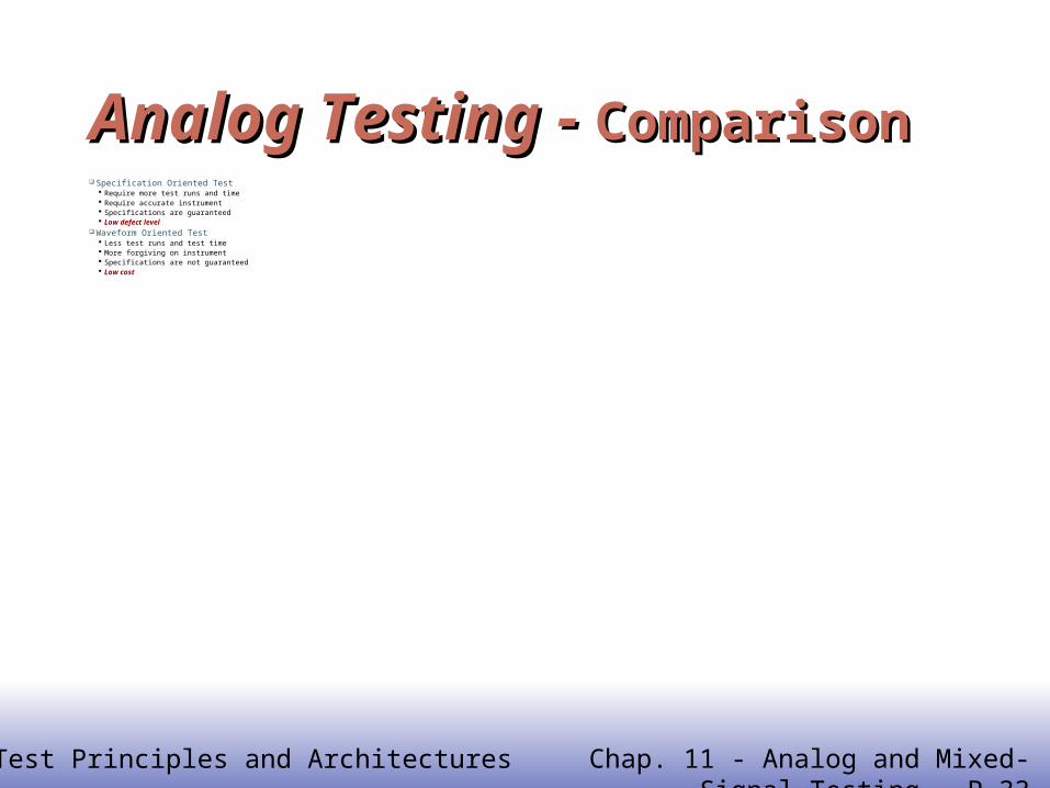
Analog Testing - Analog Testing - ComparisonComparison Specification Oriented Test
Require more test runs and time Require accurate instrument Specifications are guaranteed Low defect level
Waveform Oriented Test Less test runs and test time More forgiving on instrument Specifications are not guaranteed Low cost

EE14134
VLSI Test Principles and Architectures Chap. 11 - Analog and Mixed-Signal Testing - P.34
11.2 Analog Circuit Testing11.2 Analog Circuit Testing
Analog Test Approaches Analog Test Waveforms DC Parametric Testing AC Parametric Testing

EE14135
VLSI Test Principles and Architectures Chap. 11 - Analog and Mixed-Signal Testing - P.35
Analog Test WaveformsAnalog Test Waveforms
Sine Square (Step) Ramp Triangular
Chirp (Sweep Sine) Arbitrary Modulated

EE14136
VLSI Test Principles and Architectures Chap. 11 - Analog and Mixed-Signal Testing - P.36
For transient response testing Application: Filter, OPs, VCO, etc Difficult to generate good steps
Waveform - StepWaveform - Step
Trr
r
oo
Tf
Tf
5.3
1)3~4(
160~45

EE14137
VLSI Test Principles and Architectures Chap. 11 - Analog and Mixed-Signal Testing - P.37
Step change in voltage: Transient testing Step change in frequency: PLL testing Step change in amplitude: AGC testing
Waveform - StepWaveform - Step
Frequency StepVoltage Step Amplitude Step
EE14138
VLSI Test Principles and Architectures Chap. 11 - Analog and Mixed-Signal Testing - P.38
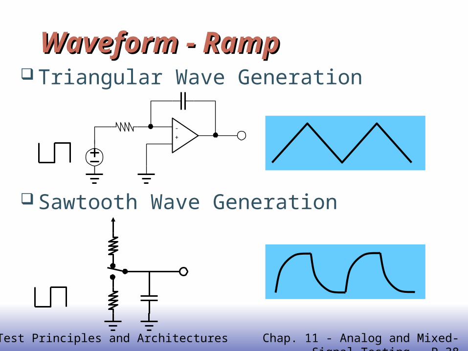
Waveform - RampWaveform - Ramp
Sawtooth Wave Generation
-
+
Triangular Wave Generation

EE14139
VLSI Test Principles and Architectures Chap. 11 - Analog and Mixed-Signal Testing - P.39
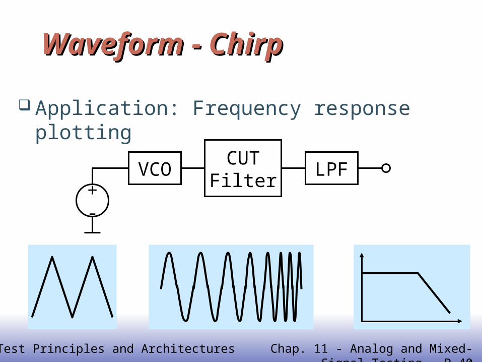
Also called Sweep Sine Generation: Triangular to VCO Application: Frequency response plotting
Waveform - ChirpWaveform - Chirp
+-
VCO Chirp
EE14140
VLSI Test Principles and Architectures Chap. 11 - Analog and Mixed-Signal Testing - P.40
Application: Frequency response plotting
Waveform - ChirpWaveform - Chirp
+-
VCOCUTFilter
LPF

EE14141
VLSI Test Principles and Architectures Chap. 11 - Analog and Mixed-Signal Testing - P.41
Synthesized by DACsCombinations of all kinds of waveform
Waveform - ArbitraryWaveform - Arbitrary
DAC LPF

EE14142
VLSI Test Principles and Architectures Chap. 11 - Analog and Mixed-Signal Testing - P.42
Modulated/Synthesized Waveforms Communication System Testing
–GSM, CDMA, 1394, USB2, etc.
Modulation–AM, FM, PCM, PWM, QAM, PSK, QPSK
Generated by dedicated instrument
Waveform - Waveform - Modulated/SynthesizedModulated/Synthesized

EE14143
VLSI Test Principles and Architectures Chap. 11 - Analog and Mixed-Signal Testing - P.43
11.2 Analog Circuit Testing11.2 Analog Circuit Testing
Analog Test Approaches Analog Test WaveformsDC Parametric Testing AC Parametric Testing

EE14144
VLSI Test Principles and Architectures Chap. 11 - Analog and Mixed-Signal Testing - P.44
DC Parametric TestingDC Parametric TestingRated output current Rated output voltage
Open-loop gain Slewing rate
Unity gain full power response
Unity gain small signal response
Overload recovery Input bias current
Input offset voltage Input offset current
Input noise Input impedance
Supply voltage sensitivity Common mode rejection
Maximum voltage between inputs
Maximum common mode voltage
Temperature drift Source: [Sata 1967]

EE14145
VLSI Test Principles and Architectures Chap. 11 - Analog and Mixed-Signal Testing - P.45
DC Test – DC Test – Open-Loop Gain MeasurementOpen-Loop Gain Measurement
y
xo V
VA
101
Vi
10K 10K
10K
100
100
y
xo V
VA
101
OctavedB /6
102 103 104 105 106101
20
80
60
40 Ao
tf
dBf3
o
oL I
VR
yV xV
EE14146
VLSI Test Principles and Architectures Chap. 11 - Analog and Mixed-Signal Testing - P.46
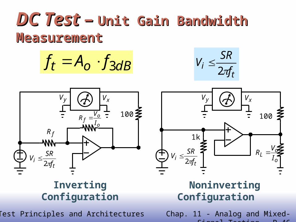
DC Test – DC Test – Unit Gain Bandwidth MeasurementUnit Gain Bandwidth Measurement
dBot fAf 3
100
ti f
SRV
2
o
of I
VR
fR
Inverting Configuration
1k
100
ti f
SRV
2
o
oL I
VR
yV xV yV xV
Noninverting Configuration
ti f
SRV
2

EE14147
VLSI Test Principles and Architectures Chap. 11 - Analog and Mixed-Signal Testing - P.47
DC Test – DC Test – Common Mode Rejection RatioCommon Mode Rejection Ratio
100
CMV
R1
R1R2
R2
oVCMV
1
2/R
RV
A
VV o
o
oiCM
)/log(20CM
oo V
VACMRR

EE14148
VLSI Test Principles and Architectures Chap. 11 - Analog and Mixed-Signal Testing - P.48
DC Test – DC Test – Power Supply Rejection RatioPower Supply Rejection Ratio
)/log(20DD
oo V
VAPSRR
DDV
oVDDV
EE14149
VLSI Test Principles and Architectures Chap. 11 - Analog and Mixed-Signal Testing - P.49
11.2 Analog Circuit Testing11.2 Analog Circuit Testing
Analog Test Approaches Analog Test Waveforms DC Parametric Testing AC Parametric Testing
EE14150
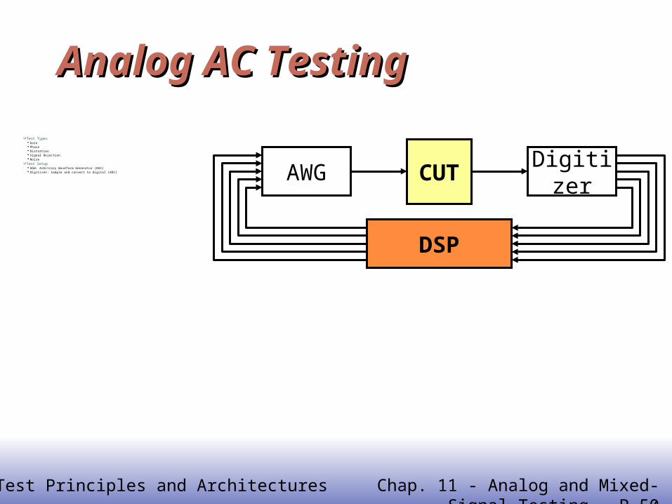
VLSI Test Principles and Architectures Chap. 11 - Analog and Mixed-Signal Testing - P.50
Test Types Gain Phase Distortion Signal Rejection Noise
Test Setup AGW: Arbitrary Waveform Generator (DAC) Digitizer: Sample and convert to digital (ADC)
Analog AC TestingAnalog AC Testing
AWG CUT Digitizer
DSP

EE14151
VLSI Test Principles and Architectures Chap. 11 - Analog and Mixed-Signal Testing - P.51
Input sine wave (1KHz) with fixed amplitude Digitize the output waveform DSP (FFT) to eliminate distortion and noise. Check the fundamental amplitude. Detect first order defects in a circuit. Voltage in dBV or dBm
AC – AC – Maximal Output AmplitudeMaximal Output Amplitude
DUTAWG Digitizer
VPP
Clipped
DSP
EE14152
VLSI Test Principles and Architectures Chap. 11 - Analog and Mixed-Signal Testing - P.52
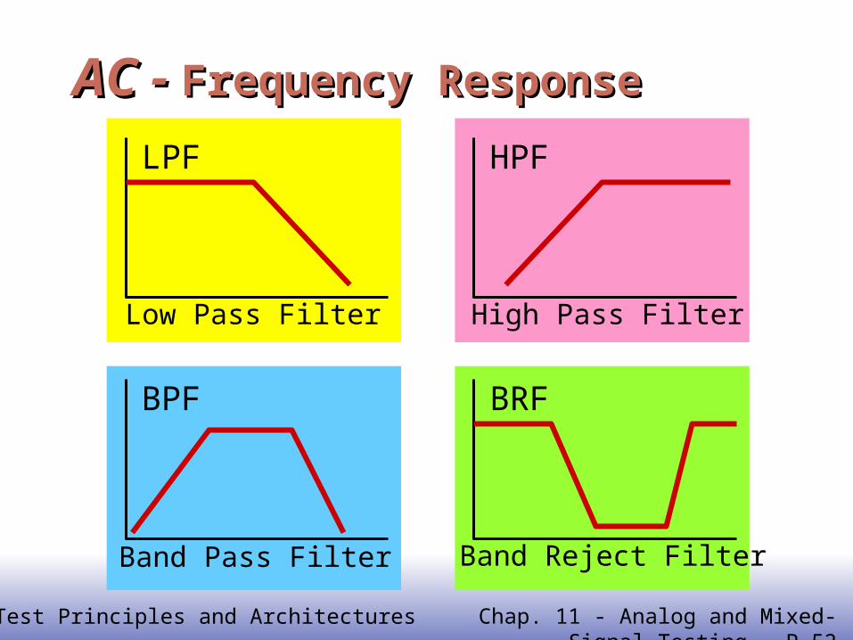
AC - AC - Frequency ResponseFrequency Response
LPF
Low Pass Filter
HPF
High Pass Filter
BPF
Band Pass Filter
BRF
Band Reject Filter

EE14153
VLSI Test Principles and Architectures Chap. 11 - Analog and Mixed-Signal Testing - P.53
AC - AC - Frequency ResponseFrequency Response
A (dB)
101 102 103 104 105 106 107
0
-45
-90
-135
-180
Phase
40
20
0
-20
-40
-20dB/dec
-40dB/dec
-20dB/dec
-45/dec
45/dec
))((
)()(
42
62
10
jw1
10
jw1
10
jw110
jwA
• Open Loop Gain 102
• Pole 1: 102
• Pole 2: 104
• Zero: 106
Bode Plot

EE14154
VLSI Test Principles and Architectures Chap. 11 - Analog and Mixed-Signal Testing - P.54
AC - AC - Frequency ResponseFrequency Response
Pass BandStop Band Stop Band
F
A(dB)Pass Band Ripple
Stop BandRejection
Stop BandRejection

EE14155
VLSI Test Principles and Architectures Chap. 11 - Analog and Mixed-Signal Testing - P.55
AC - AC - Frequency ResponseFrequency Response
F
A(dB)
Upper LimitMask
Lower LimitMask

EE14156
VLSI Test Principles and Architectures Chap. 11 - Analog and Mixed-Signal Testing - P.56
AC - AC - Frequency ResponseFrequency ResponseFrequencies of special interests

EE14157
VLSI Test Principles and Architectures Chap. 11 - Analog and Mixed-Signal Testing - P.57
AC - AC - Frequency ResponseFrequency Response
•Multi-tone Test Waveform
ki
1iiii tAtA )sin()(

EE14158
VLSI Test Principles and Architectures Chap. 11 - Analog and Mixed-Signal Testing - P.58
AC - AC - Frequency ResponseFrequency Response
•Multi-tone Test Waveform
ki
1iiii tAtA )sin()(

EE14159
VLSI Test Principles and Architectures Chap. 11 - Analog and Mixed-Signal Testing - P.59
•Distortion•Harmonic Distortion• Intermodulation Distortion•Crossover
•Cause•Nonlinearity of the circuit•Clip (saturation)•Mismatch of the devices
AC – AC – Noise and DistortionNoise and Distortion
EE14160
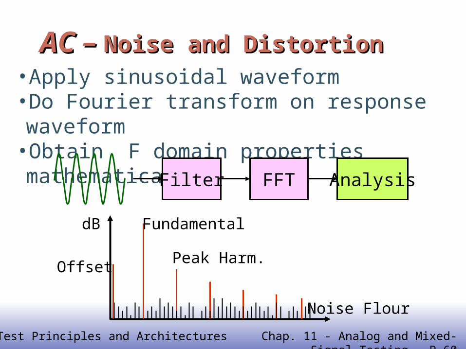
VLSI Test Principles and Architectures Chap. 11 - Analog and Mixed-Signal Testing - P.60
AC – AC – Noise and DistortionNoise and Distortion•Apply sinusoidal waveform•Do Fourier transform on response waveform
•Obtain F domain properties mathematically. Filter FFT
dB Fundamental
Peak Harm.
Noise Flour
Offset
Analysis

EE14161
VLSI Test Principles and Architectures Chap. 11 - Analog and Mixed-Signal Testing - P.61
AC – AC – Noise and DistortionNoise and Distortion
dBFundamental
Harmonics
DCOffset
F
NoiseF
H2 H3H4
H5Ni
2
2log10
iN
FSNR%100log10
2
2
2
2
ii H
F
H
FTHD
22
2log10
ii NH
FSNDR

EE14162
VLSI Test Principles and Architectures Chap. 11 - Analog and Mixed-Signal Testing - P.62
AC – AC – Intermodulation DistortionIntermodulation Distortion
tfAtfAtv 2211 2sin2sin)(
2 4 6 8 10 12 14 16 18 200 22 24
f2 – f12f1 – f2 2f 2 – f1
f1 f2
f1 + f2
2f12f2
3f1 3f 2
7 8
f1 f2
EE14163
VLSI Test Principles and Architectures Chap. 11 - Analog and Mixed-Signal Testing - P.63
Studied the analog test approaches Specification oriented testing Waveform oriented testing
Outlined the analog test waveforms Sine, step, triangular, chirp, arbitrary, modulated
Discussed DC parametric testing Open-loop gain, unit gain bandwidth CMRR, PSRR
Discussed AC parametric testing Use AWG, Digitizer, and DSP Frequency response, Noise, and Distortion
11.2 Summary11.2 Summary
EE14164
VLSI Test Principles and Architectures Chap. 11 - Analog and Mixed-Signal Testing - P.64
11.3 Mixed-Signal Testing 11.3 Mixed-Signal Testing
Introduction to Analog-Digital Conversion ADC and DAC Circuit Structure ADC/DAC Specification and Fault Models IEEE Std. 1057 Time-Domain ADC Testing Frequency-Domain ADC Testing
EE141VLSI Test Principles and Architectures Chap. 11 - Analog and Mixed-Signal Testing - P.65
X in
X out LSBs121110
9876543210
1 2 3 4
1
2
3
4
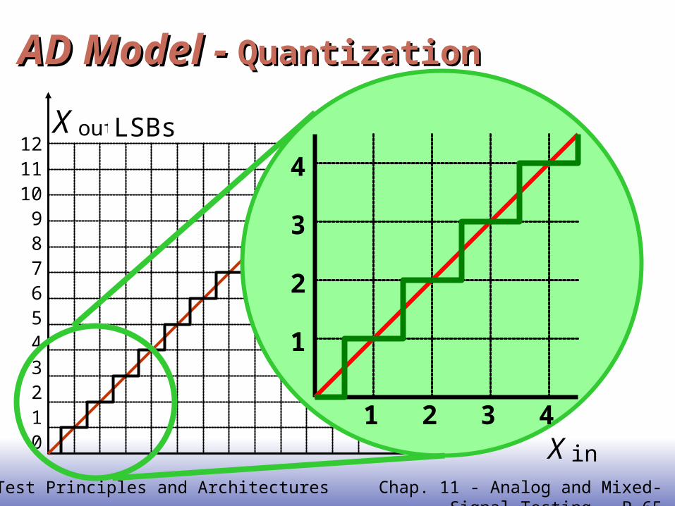
AD Model - AD Model - QuantizationQuantization
X in

EE14166
VLSI Test Principles and Architectures Chap. 11 - Analog and Mixed-Signal Testing - P.66
• Quantization error is sawtooth-like. • Uniform distribute between (-q/2, q/2) (q=LSB).
q
)t(x Original signal Quantized signal
t
t
2/q
2/q
)t(nq Quantization error
Quantizatoin – Quantizatoin – Noise ModelNoise Model

EE14167
VLSI Test Principles and Architectures Chap. 11 - Analog and Mixed-Signal Testing - P.67
• The error contains a lot of jumps.• Error spectral is much wider than the original signal.• The bandwidth of the quantization is proportional to
the slop of the signal and inversely proportional to the quantum size q.
Quantizatoin – Quantizatoin – Noise ModelNoise Model
t
2/q
2/q
)t(nq Quantization error

EE14168
VLSI Test Principles and Architectures Chap. 11 - Analog and Mixed-Signal Testing - P.68
A sine wave is quantized by a B-bit ADC. How large is the SNR.
Quantization Quantization - Noise Model - Noise Model
qVpn22
2
2p
S
VP
123
22
2
PN
q
)t(x
Original signal
Quantized signal
t
t
2/q
2/q
)t(nq Quantization error

EE14169
VLSI Test Principles and Architectures Chap. 11 - Analog and Mixed-Signal Testing - P.69
Quantization Quantization - Noise Model - Noise Model
)46log(10
12
2log10log10 12
2
n
p
N
s
q
V
P
PSNR
dBSNR 8.61 For n=10,
dBnSNR )676.1(

EE14170
VLSI Test Principles and Architectures Chap. 11 - Analog and Mixed-Signal Testing - P.70
11.3 Mixed-Signal Testing 11.3 Mixed-Signal Testing
Introduction to Analog-Digital Conversion ADC and DAC Circuit Structure ADC/DAC Specification and Fault Models IEEE Std. 1057 Time-Domain ADC Testing Frequency-Domain ADC Testing
EE14171
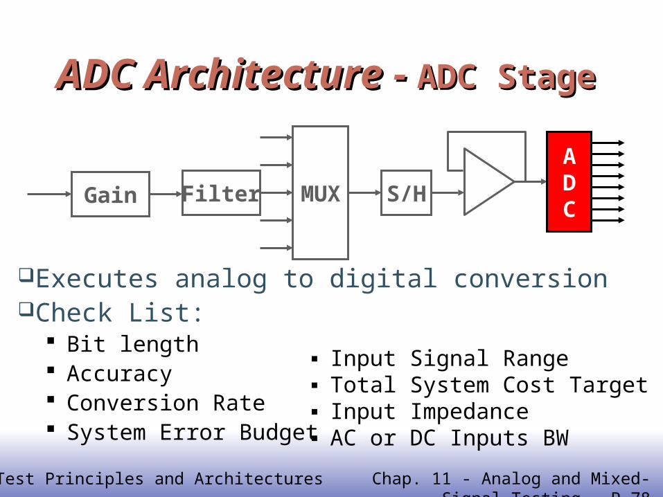
VLSI Test Principles and Architectures Chap. 11 - Analog and Mixed-Signal Testing - P.71
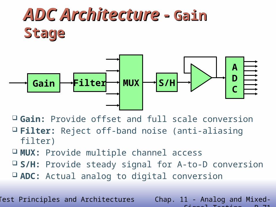
ADC Architecture - ADC Architecture - Gain StageGain Stage
Gain Filter MUX S/H
ADC
Gain: Provide offset and full scale conversion Filter: Reject off-band noise (anti-aliasing filter) MUX: Provide multiple channel access S/H: Provide steady signal for A-to-D conversion ADC: Actual analog to digital conversion
EE14172
VLSI Test Principles and Architectures Chap. 11 - Analog and Mixed-Signal Testing - P.72
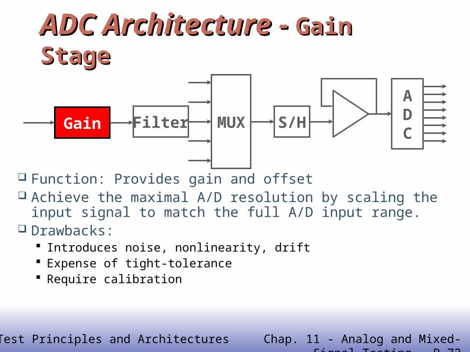
ADC Architecture - ADC Architecture - Gain StageGain Stage
Gain Filter MUX S/H
ADC
Function: Provides gain and offset Achieve the maximal A/D resolution by scaling the input signal to
match the full A/D input range. Drawbacks:
Introduces noise, nonlinearity, drift Expense of tight-tolerance Require calibration

EE14173
VLSI Test Principles and Architectures Chap. 11 - Analog and Mixed-Signal Testing - P.73
ADC Architecture - ADC Architecture - Filter StageFilter Stage
Gain Filter MUX S/H
ADC
Function: Attenuate the out-of-band noise to prevent aliasing
Filter Position Before the MUX (1 per channel) : maximize speed in
switching channels. After the MUX: minimize mismatching among channels.

EE14174
VLSI Test Principles and Architectures Chap. 11 - Analog and Mixed-Signal Testing - P.74
ADC Architecture - ADC Architecture - Filter StageFilter Stage
Anti-Aliasing Filter
A(w) A(w) A(w)
Signal Spectrum
Nyquist Rate Sampling
4X Over Sampling
Anti Aliasing Filter Anti Aliasing Filter

EE14175
VLSI Test Principles and Architectures Chap. 11 - Analog and Mixed-Signal Testing - P.75
ADC Architecture - ADC Architecture - MUX StageMUX Stage
Gain Filter MUX S/H
ADC
Function: Provides multiple access Crosstalk:
The most severe problem Frequency dependent Can be minimized by placing amplifier before the MUX.
Load Issues Avoid too many fanins. Use hierarchical structure.

EE14176
VLSI Test Principles and Architectures Chap. 11 - Analog and Mixed-Signal Testing - P.76
ADC Architecture - ADC Architecture - S/H StageS/H Stage
Gain Filter MUX S/H
ADC
Function: Provides steady signal Provides signal synchronization,
S/H position: After the MUX for cost reason Before MUX for synchronization and
crosstalk reduction.
MUX
S/H
S/H
S/H
S/H
EE14177
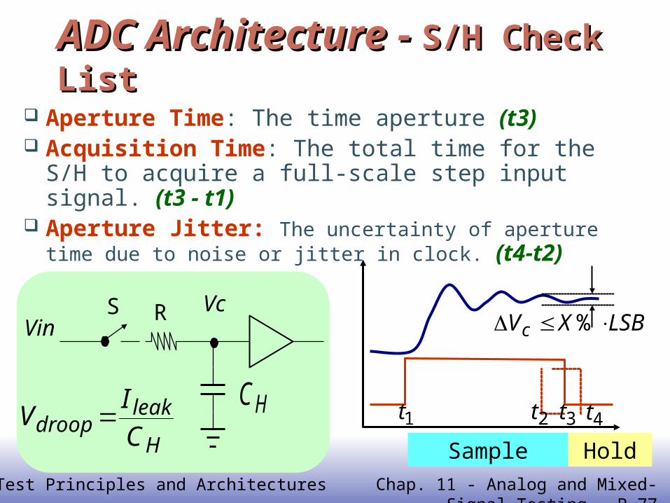
VLSI Test Principles and Architectures Chap. 11 - Analog and Mixed-Signal Testing - P.77
ADC Architecture - ADC Architecture - S/H Check ListS/H Check List Aperture Time: The time aperture (t3) Acquisition Time: The total time for the S/H to
acquire a full-scale step input signal. (t3 - t1) Aperture Jitter: The uncertainty of aperture time due to
noise or jitter in clock. (t4-t2)
Sample Hold
1t 2t 3t 4t
LSBXVc %S
VinVc
HC
R
H
leakdroop C
IV
EE14178
VLSI Test Principles and Architectures Chap. 11 - Analog and Mixed-Signal Testing - P.78
ADC Architecture - ADC Architecture - ADC StageADC Stage
Gain Filter MUX S/H
ADC
Executes analog to digital conversionCheck List:
Bit length Accuracy Conversion Rate System Error Budget
▪ Input Signal Range▪ Total System Cost Target▪ Input Impedance▪ AC or DC Inputs BW
EE14179
VLSI Test Principles and Architectures Chap. 11 - Analog and Mixed-Signal Testing - P.79
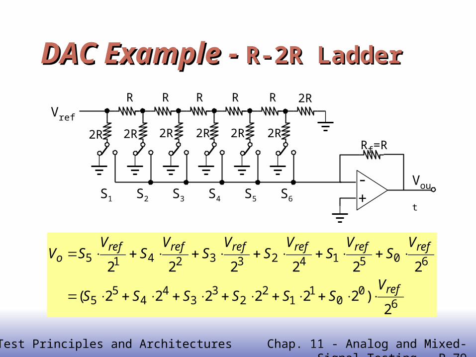
DAC Example - DAC Example - R-2R LadderR-2R Ladder
-+
Vref
S1 S2 S3 S4 S5 S6
2R 2RRf=R
Vout
2R 2R 2R 2R
2RRR R R R
60
01
12
23
34
45
5
605142332415
2)222222(
222222
ref
refrefrefrefrefrefo
VSSSSSS
VS
VS
VS
VS
VS
VSV
EE14180
VLSI Test Principles and Architectures Chap. 11 - Analog and Mixed-Signal Testing - P.80
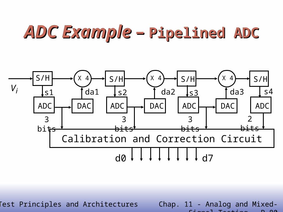
ADC Example – ADC Example – Pipelined ADCPipelined ADC
S/H
ADC DAC
X 4
3 bits
S/H
ADC
X 4
3 bits
S/H
ADC DAC
X 4
3 bits
S/H
ADC
2 bits
DAC
s1 s2 s3 s4da3da2da1iV
Calibration and Correction Circuit
d0 d7

EE14181
VLSI Test Principles and Architectures Chap. 11 - Analog and Mixed-Signal Testing - P.81
ADC – ADC – Bits v.s. ThroughputBits v.s. Throughput
ADC Bit-Length Throughput
Flash ~ 6 bits 100 M ~
Pipelined 8 ~ 16 bits 10 ~ 100 MHz
Sigma-Delta 14 ~ bits ~ 10 M
EE14182
VLSI Test Principles and Architectures Chap. 11 - Analog and Mixed-Signal Testing - P.82
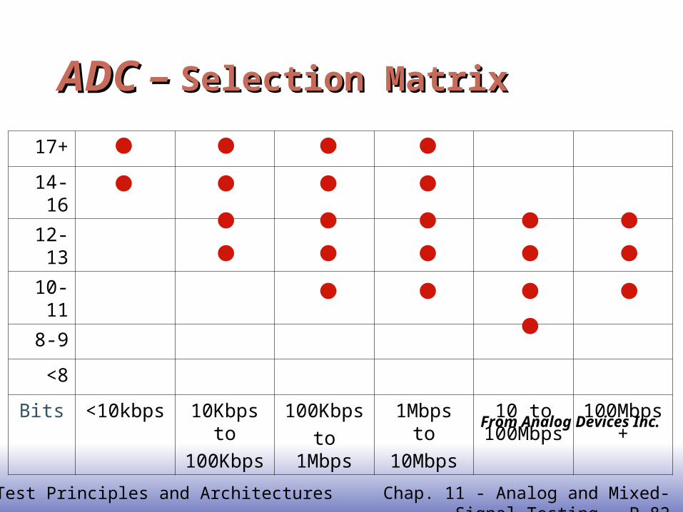
ADC – ADC – Selection MatrixSelection Matrix
17+
14-16
12-13
10-11
8-9
<8
Bits <10kbps 10Kbps to
100Kbps
100Kbps
to 1Mbps
1Mbps to
10Mbps
10 to 100Mbps
100Mbps+
From Analog Devices Inc.

EE14183
VLSI Test Principles and Architectures Chap. 11 - Analog and Mixed-Signal Testing - P.83
ADC – ADC – Example Example AD775AD775
From Analog Devices Inc.

EE14184
VLSI Test Principles and Architectures Chap. 11 - Analog and Mixed-Signal Testing - P.84
11.3 Mixed-Signal Testing 11.3 Mixed-Signal Testing
Introduction to Analog-Digital Conversion ADC and DAC Circuit Structure ADC/DAC Specification and Fault Models IEEE Std. 1057 Time-Domain ADC Testing Frequency-Domain ADC Testing
EE14185
VLSI Test Principles and Architectures Chap. 11 - Analog and Mixed-Signal Testing - P.85
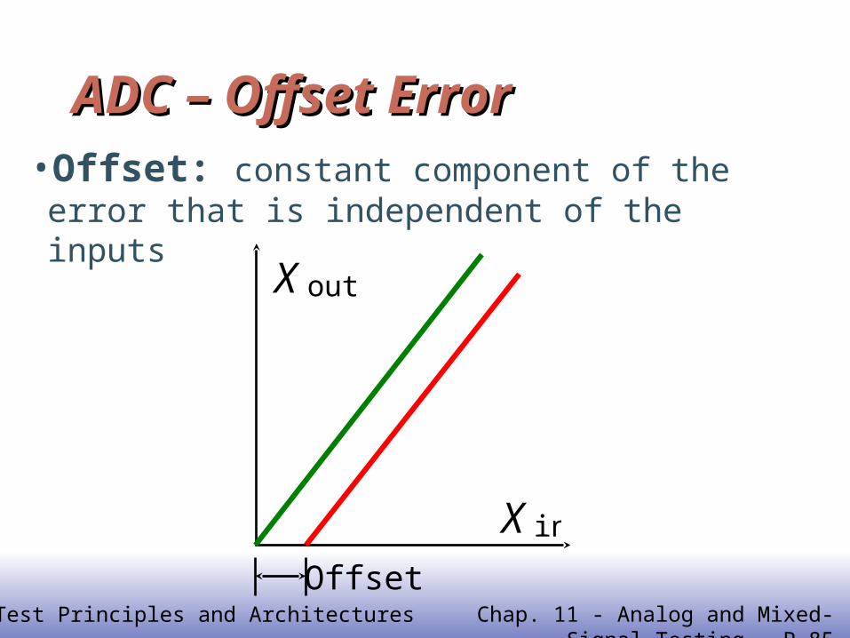
ADC – Offset ErrorADC – Offset Error
Offset
X in
X out
•Offset: constant component of the error that is independent of the inputs

EE14186
VLSI Test Principles and Architectures Chap. 11 - Analog and Mixed-Signal Testing - P.86
ADC – Gain ErrorADC – Gain Error
X in
X out
•Gain Error: difference between the actual transfer ratio and the ideal ratio
• Also called Calibration Error

EE14187
VLSI Test Principles and Architectures Chap. 11 - Analog and Mixed-Signal Testing - P.87
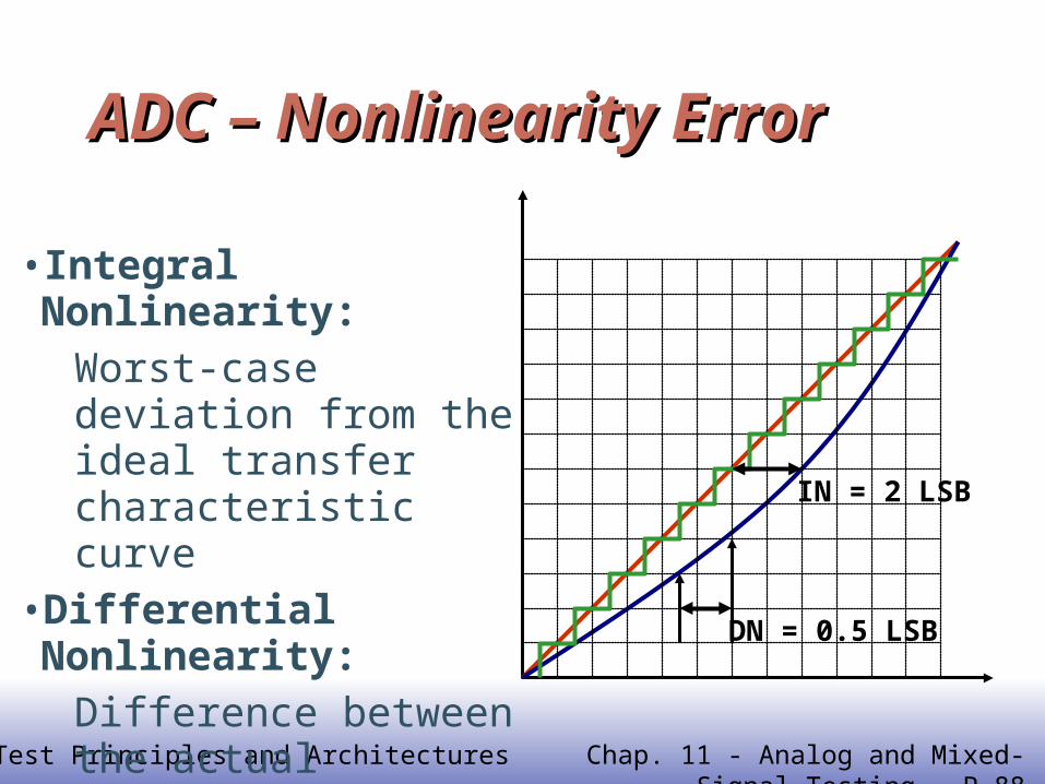
ADC – Nonlinearity ErrorADC – Nonlinearity Error
X in
X out
•Nonlinearity error: The deviation of the output quantity from a specified linear reference
EE14188
VLSI Test Principles and Architectures Chap. 11 - Analog and Mixed-Signal Testing - P.88
ADC – Nonlinearity ErrorADC – Nonlinearity Error
• Integral Nonlinearity:Worst-case deviation from the ideal transfer characteristic curve
• Differential Nonlinearity:Difference between the actual transfer ratio and the ideal ratio
IN = 2 LSB
DN = 0.5 LSB

EE14189
VLSI Test Principles and Architectures Chap. 11 - Analog and Mixed-Signal Testing - P.89
ADC – Temperature-Dependent ErrorADC – Temperature-Dependent Error•Temperature-Dependent Error: Due to the change in ambient temperature or temperature variation due to self-heating (temperature stability, temperature coefficient)
X in
X out T 3
T 2
T1

EE14190
VLSI Test Principles and Architectures Chap. 11 - Analog and Mixed-Signal Testing - P.90
ADC – Load-Dependent ErrorADC – Load-Dependent Error
•Load Error: Loading error is due to the effect of a load impedance upon the converter or signal source driving it.
X in
X out RL1
RL2RL1RL1
EE14191
VLSI Test Principles and Architectures Chap. 11 - Analog and Mixed-Signal Testing - P.91
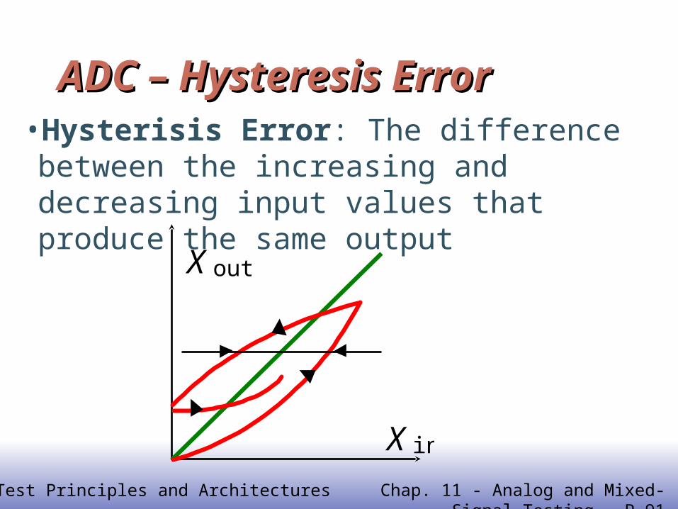
ADC – Hysteresis ErrorADC – Hysteresis Error
X in
X out
•Hysterisis Error: The difference between the increasing and decreasing input values that produce the same output

EE14192
VLSI Test Principles and Architectures Chap. 11 - Analog and Mixed-Signal Testing - P.92
ADC – Resolution ErrorADC – Resolution Error
X in
X out
• Resolution Error: The error due to the inability to respond to change of a variable smaller than a given increment

EE14193
VLSI Test Principles and Architectures Chap. 11 - Analog and Mixed-Signal Testing - P.93
ADC – Missing Code ErrorADC – Missing Code Error
Missing Codes
Ideal Input Waveform
Quantized with missing Code
Quantization Error

EE14194
VLSI Test Principles and Architectures Chap. 11 - Analog and Mixed-Signal Testing - P.94
11.3 Mixed-Signal Testing 11.3 Mixed-Signal Testing
Introduction to Analog-Digital Conversion ADC and DAC Circuit Structure ADC/DAC Specification and Fault Models IEEE Std. 1057 Time-Domain ADC Testing Frequency-Domain ADC Testing
EE14195
VLSI Test Principles and Architectures Chap. 11 - Analog and Mixed-Signal Testing - P.95
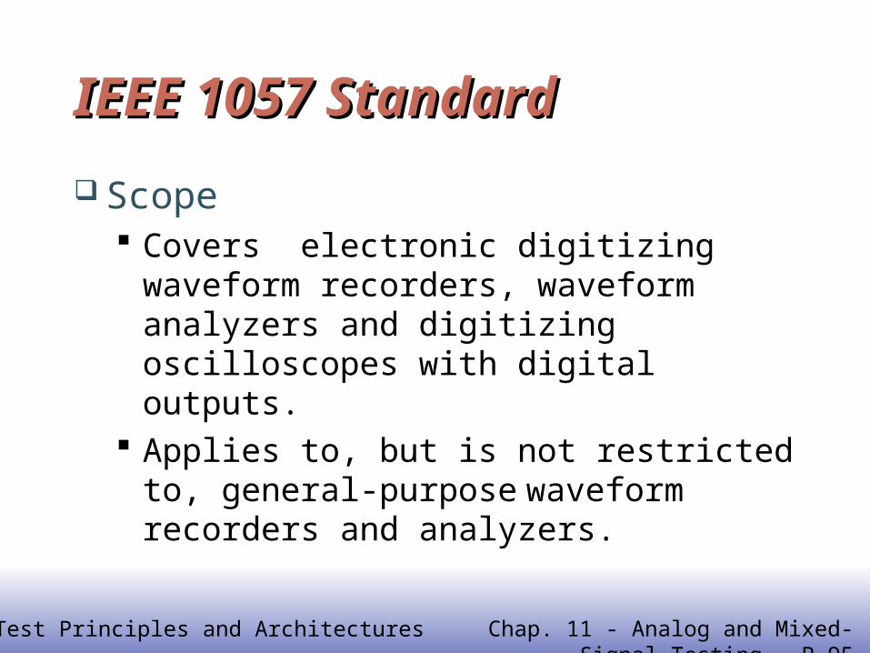
IEEE 1057 StandardIEEE 1057 Standard
Scope Covers electronic digitizing waveform
recorders, waveform analyzers and digitizing oscilloscopes with digital outputs.
Applies to, but is not restricted to, general-purpose waveform recorders and analyzers.

EE14196
VLSI Test Principles and Architectures Chap. 11 - Analog and Mixed-Signal Testing - P.96
IEEE 1057 StandardIEEE 1057 Standard
Purpose Provides common methods for testing and
terminology for describing the performance of waveform recorders.
Benefits users and manufacturers of such devices.
Presents many performance features, sources of error, and test methods.

EE14197
VLSI Test Principles and Architectures Chap. 11 - Analog and Mixed-Signal Testing - P.97
IEEE 1057 – IEEE 1057 – General InformationGeneral Information
Model Number
Dimensions and weight
Power Requirement
Environmental conditions (tem., humidity, EMC/EMI, etc.)
Any special or peculiar characteristics
Available options and accessories
Exception to the above parameters where applicable
Calibration interval

EE14198
VLSI Test Principles and Architectures Chap. 11 - Analog and Mixed-Signal Testing - P.98
IEEE 1057 – IEEE 1057 – Minimum SpecificationMinimum Specification
Number of digitizing bits Input impedance
Sample rates Analog bandwidth
Memory length Input signal ranges

EE14199
VLSI Test Principles and Architectures Chap. 11 - Analog and Mixed-Signal Testing - P.99
IEEE 1057 – IEEE 1057 – Additional SpecificationsAdditional SpecificationsGain Fixed error in sample time
Offset Trigger delay and jitter
Differential nonlinearity Trigger sensitivity
Integral nonlinearity Trigger minimum rate of change
Harmonic distortion Trigger hysteresis band
Spurious response Trigger coupling to signal
Maximal static error Crosstalk
Signal to noise ratio Monotonicity
Effective bits Hystersis
Peak error Over voltage recovery
Random noise Word error rate
Frequency response Cycle time
Settling time Common mode rejection ratio
Slew limit Differential input impedance
Overshoot and precursors Maximum operating common
Aperture uncertainty mode signal level
Long-term stability Transition duration of step response
Maximum common mode signal level

EE141100
VLSI Test Principles and Architectures Chap. 11 - Analog and Mixed-Signal Testing - P.100
IEEE 1057 – IEEE 1057 – Test MethodsTest Methods
General methods Triggering
Input impedance Crosstalk
Gain and offset Monotonicity
Noise Hysteresis
Analog bandwidth Overvoltage Recovery
Frequency response Word Error Rate
Step Response parameters Cycle Time
Time base errors Differential Input Specification
Linearity, harmonic distortion, and spurious responses

EE141101
VLSI Test Principles and Architectures Chap. 11 - Analog and Mixed-Signal Testing - P.101
11.3 Mixed-Signal Testing 11.3 Mixed-Signal Testing
Introduction to Analog-Digital Conversion ADC and DAC Circuit Structure ADC/DAC Specification and Fault Models IEEE Std. 1057 Time-Domain ADC Testing Frequency-Domain ADC Testing
EE141102
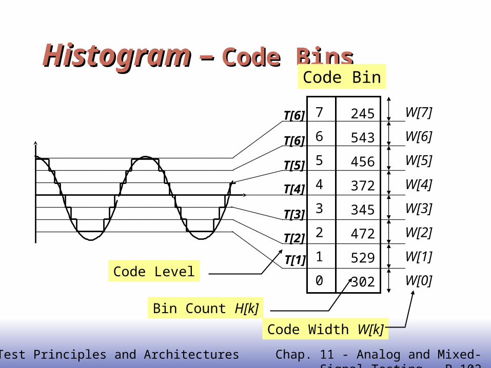
VLSI Test Principles and Architectures Chap. 11 - Analog and Mixed-Signal Testing - P.102
Histogram – Histogram – Code BinsCode BinsCode Bin
T[1]
T[2]
T[6]
T[6]
T[5]
T[4]
T[3]
7
6
5
4
3
2
1
0
W[7]
W[6]
W[5]
W[4]
W[3]
W[2]
W[1]
W[0]Code Level
Code Width W[k]
245
543
456
372
345
472
529
302
Bin Count H[k]
EE141103
VLSI Test Principles and Architectures Chap. 11 - Analog and Mixed-Signal Testing - P.103
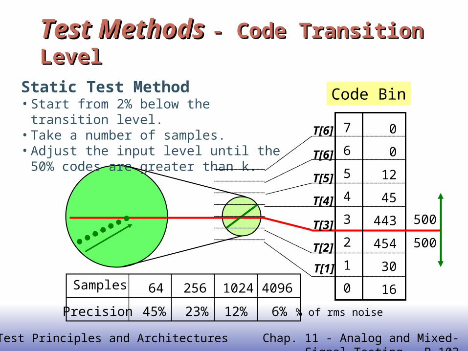
Test Methods Test Methods - Code Transition Level- Code Transition Level
Code Bin
T[1]
T[2]
T[6]
T[6]
T[5]
T[4]
T[3]
7
6
5
4
3
2
1
0
0
0
12
45
443
454
30
16
Static Test Method• Start from 2% below the transition level.• Take a number of samples.• Adjust the input level until the 50% codes
are greater than k.
Samples
Precision
64
45%
256
23%
1024
12%
4096
6% % of rms noise
500
500

EE141104
VLSI Test Principles and Architectures Chap. 11 - Analog and Mixed-Signal Testing - P.104
Test Methods Test Methods - Code Transition Level- Code Transition LevelDynamic Test Method• Apply full range sine wave• Calculate the transition level from the bin count
T[1]
T[2]
T[6]
T[6]
T[5]
T[4]
T[3]
7
6
5
4
3
2
1
0
245
543
456
372
345
472
529
302
M
kHACkT c ]1[
cos][
• A: Amplitude C: Offset• H[j]: The code count of bin j.• M: Total number of samples • Record Length M and Number of Cycles Mc must not have common term.
j
ic iHjH
0][][

EE141105
VLSI Test Principles and Architectures Chap. 11 - Analog and Mixed-Signal Testing - P.105
Test Methods Test Methods - Gain and Offset- Gain and Offset• Apply a slow ramp signal• Construct the code bin table
1)1(][][ TkQkVkTG os
T[1]
T[2]
T[6]
T[6]
T[5]
T[4]
T[3]
7
6
5
4
3
2
1
0
203
443
440
435
439
429
447
330
Q: ideal width of the code bin
12
1
212
1
2
12
1
1
12
1
212
1
2
12
1
12
212
12
12
N N
N
N N
N
k k
N
k
NN
k k
N
k
N
kTkT
kT
Q
kTkT
kkT
QG
12
11 12
12N
kN
Nos kT
GQTV

EE141106
VLSI Test Principles and Architectures Chap. 11 - Analog and Mixed-Signal Testing - P.106
Test Methods Test Methods - Gain and Offset (Example)- Gain and Offset (Example)
Ideal Gain Error Offset Error
Transfer Curves
Histograms
128 128 128 128
Game/Offset

EE141107
VLSI Test Principles and Architectures Chap. 11 - Analog and Mixed-Signal Testing - P.107
Test Methods Test Methods - Nonlinearity- Nonlinearity
Q
QkWGDNL
Q
QkWGkDNL
max
NQ
TkQkTMSE
2
1max100 1
NQ
kINL
2
max100
Differential Nonlinearity
IntegralNonlinearity
MaximalStatic Error
T[1]
T[2]
T[6]
T[6]
T[5]
T[4]
T[3]
7
6
5
4
3
2
1
0
203
443
440
435
439
429
447
330
EE141108
VLSI Test Principles and Architectures Chap. 11 - Analog and Mixed-Signal Testing - P.108
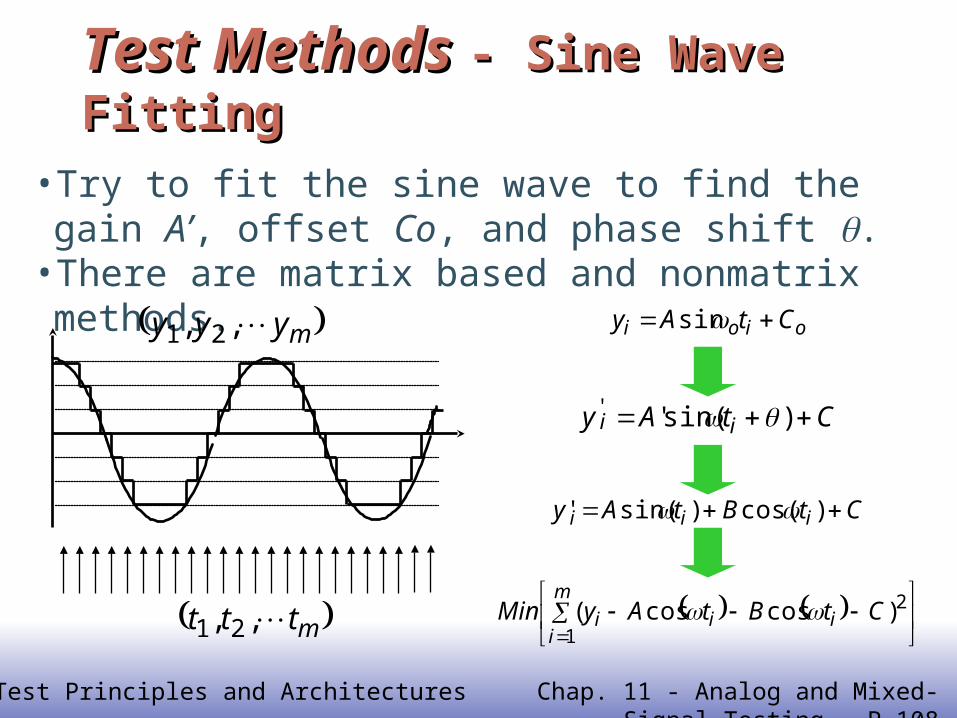
Test Methods Test Methods - Sine Wave Fitting- Sine Wave Fitting
oioi CtAy sin
• Try to fit the sine wave to find the gain A’, offset Co, and phase shift .
• There are matrix based and nonmatrix methods. myyy ,, 21
mttt ,, 21
m
iiii CtBtAyMin
1
2)coscos(
CtAy ii )sin(''
CtBtAy iii )cos()sin('

EE141109
VLSI Test Principles and Architectures Chap. 11 - Analog and Mixed-Signal Testing - P.109
Test Methods Test Methods - Sine Wave Fitting- Sine Wave Fitting
ooo CtAty )sin()(
CtBtAty )cos()sin()('
o
o
A
ABA 22
oCC
A
B1tan
o
o
)(
Original Signal:
Curve Fitted:
Gain Error:
Offset Error:
Phase Error:
Frequency Error:
EE141110
VLSI Test Principles and Architectures Chap. 11 - Analog and Mixed-Signal Testing - P.110
11.3 Mixed-Signal Testing 11.3 Mixed-Signal Testing
Introduction to Analog-Digital Conversion ADC and DAC Circuit Structure ADC/DAC Specification and Fault Models IEEE Std. 1057 Time-Domain ADC Testing Frequency-Domain ADC Testing

EE141111
VLSI Test Principles and Architectures Chap. 11 - Analog and Mixed-Signal Testing - P.111
ADC – ADC – Frequency Domain TestingFrequency Domain Testing•Similar to Analog AC Testing•Apply sinusoidal waveform•Do Fourier transform on response waveform•Obtain F domain properties mathematically.
Filter FFT
dB Fundamental
Peak Harm.
Noise Flour
Offset
Analysis
EE141112
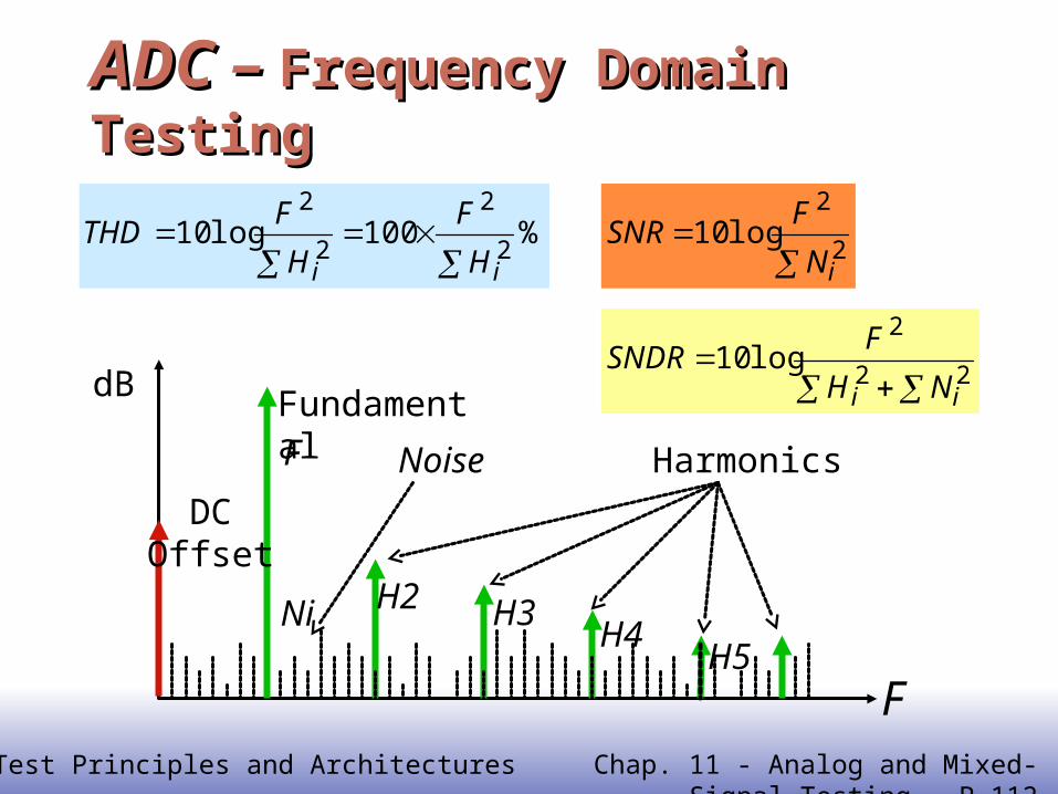
VLSI Test Principles and Architectures Chap. 11 - Analog and Mixed-Signal Testing - P.112
ADC – ADC – Frequency Domain TestingFrequency Domain Testing
dBFundamental
Harmonics
DCOffset
F
NoiseF
H2 H3H4
H5Ni
2
2log10
iN
FSNR%100log10
2
2
2
2
ii H
F
H
FTHD
22
2log10
ii NH
FSNDR

EE141113
VLSI Test Principles and Architectures Chap. 11 - Analog and Mixed-Signal Testing - P.113
11.4 IEEE Std. 1149.4 Standard for a 11.4 IEEE Std. 1149.4 Standard for a Mixed-Signal Test Bus Mixed-Signal Test Bus
IEEE Std. 1149.4 Overview IEEE Std. 1149.4 Circuit Structures IEEE Std. 1149.4 Instructions IEEE Std. 1149.4 Test Modes

EE141114
VLSI Test Principles and Architectures Chap. 11 - Analog and Mixed-Signal Testing - P.114
IEEE 1149.4 - IEEE 1149.4 - OverviewOverview Target mixed signal Printed Circuit Assembles (PCA). Components:
Mixed Signal Digital Analog Discrete
D D
A A
M MC
C
CInterconnect
DiscreteComponent
M: Mixed-signal Component A: Analog Component D: Digital Component
EE141115
VLSI Test Principles and Architectures Chap. 11 - Analog and Mixed-Signal Testing - P.115
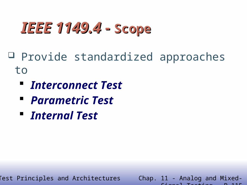
IEEE 1149.4 - IEEE 1149.4 - ScopeScope
Provide standardized approaches to Interconnect Test Parametric Test Internal Test

EE141116
VLSI Test Principles and Architectures Chap. 11 - Analog and Mixed-Signal Testing - P.116
IEEE 1149.4 IEEE 1149.4 - Interconnect Test- Interconnect Test
A
A
D
D
D
A
A
A
D
D
D
A
A
A
D
D
D
A
A
A
D
D
D
A
Open Defects Short Defects

EE141117
VLSI Test Principles and Architectures Chap. 11 - Analog and Mixed-Signal Testing - P.117
IEEE 1149.4 - IEEE 1149.4 - Parametric TestParametric Test
A
A
A
D
D-A
A
A
A
D
D-A
Simple Interconnect Extended Interconnect
EE141118
VLSI Test Principles and Architectures Chap. 11 - Analog and Mixed-Signal Testing - P.118
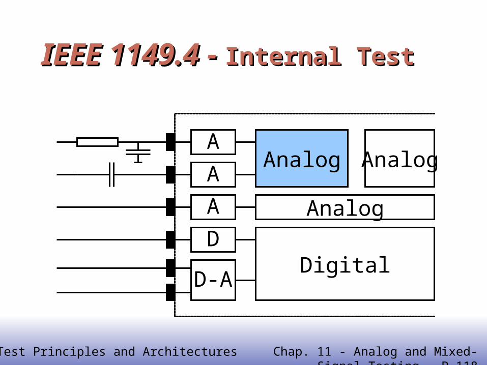
IEEE 1149.4 - IEEE 1149.4 - Internal TestInternal Test
A
A
A
D
D-A
Analog
Analog
Analog
Digital

EE141VLSI Test Principles and Architectures Chap. 11 - Analog and Mixed-Signal Testing - P.119
IEEE 1149.4 - IEEE 1149.4 - ArchitectureArchitecture
IC1 IC2 ICnIC Under Test
Analog
AT1
AT2
AB1AB2
Test Waveform Response Waveform

EE141120
VLSI Test Principles and Architectures Chap. 11 - Analog and Mixed-Signal Testing - P.120
11.4 IEEE Std. 1149.4 Standard for a 11.4 IEEE Std. 1149.4 Standard for a Mixed-Signal Test Bus Mixed-Signal Test Bus
IEEE Std. 1149.4 Overview IEEE Std. 1149.4 Circuit Structures IEEE Std. 1149.4 Instructions IEEE Std. 1149.4 Test Modes

EE141121
VLSI Test Principles and Architectures Chap. 11 - Analog and Mixed-Signal Testing - P.121
IEEE 1149.4 - IEEE 1149.4 - ArchitectureArchitecture
ICCore
DigitalBM
ABM
ABM
AnalogBM
A Pins
TBIC
Analog TAP
AT1AT2
TAP Controller1149.1
TAP
TDITDOTMSTCK
D Pins
InternalA Bus

EE141VLSI Test Principles and Architectures Chap. 11 - Analog and Mixed-Signal Testing - P.122
IEEE 1149.4 - IEEE 1149.4 - TBICTBIC
VH
VL
VTH
ABMABM
TBIC
Core
TAP
AB1AB2
AT2
Vc
AB1 AB2
Switch
AT1
AT1AT2

EE141VLSI Test Principles and Architectures Chap. 11 - Analog and Mixed-Signal Testing - P.123
IEEE 1149.4 - IEEE 1149.4 - ABMABM
AT1AT2
AB1AB2
VH VLVTH VG
A PinCD
ACUT
TBIC
ABM
ABM
TBIC
CoreCircuit
Test Control CircuitryTAP Controller
AB1AB2 AT1
AT2

EE141124
VLSI Test Principles and Architectures Chap. 11 - Analog and Mixed-Signal Testing - P.124
1149.4 – 1149.4 – Mixed-Signal ArchitectureMixed-Signal Architecture
DigitalCore
Circuit
AnalogInputs
A/D
AnalogCore
TDI TDO
AnalogOutputs
Digital
Inputs
Digital
Outputs
DBMABM
EE141125
VLSI Test Principles and Architectures Chap. 11 - Analog and Mixed-Signal Testing - P.125
11.4 IEEE Std. 1149.4 Standard for a 11.4 IEEE Std. 1149.4 Standard for a Mixed-Signal Test Bus Mixed-Signal Test Bus
IEEE Std. 1149.4 Overview IEEE Std. 1149.4 Circuit Structures IEEE Std. 1149.4 Instructions IEEE Std. 1149.4 Test Modes

EE141126
VLSI Test Principles and Architectures Chap. 11 - Analog and Mixed-Signal Testing - P.126
IEEE 1149.4 - IEEE 1149.4 - InstructionsInstructions
Mandatory Instructions BYPASS SAMPLE/PRELOAD EXTEST PROBE
Same as IEEE 1149.1

EE141127
VLSI Test Principles and Architectures Chap. 11 - Analog and Mixed-Signal Testing - P.127
IEEE 1149.4 - IEEE 1149.4 - InstructionsInstructions
Optional Instructions INTEST IDCODE/USERCODE RUNBIST CLAMP HIGHZ
Same as IEEE 1149.1
EE141128
VLSI Test Principles and Architectures Chap. 11 - Analog and Mixed-Signal Testing - P.128
11.4 IEEE Std. 1149.4 Standard for a 11.4 IEEE Std. 1149.4 Standard for a Mixed-Signal Test Bus Mixed-Signal Test Bus
IEEE Std. 1149.4 Overview IEEE Std. 1149.4 Circuit Structures IEEE Std. 1149.4 Instructions IEEE Std. 1149.4 Test Modes
EE141VLSI Test Principles and Architectures Chap. 11 - Analog and Mixed-Signal Testing - P.129
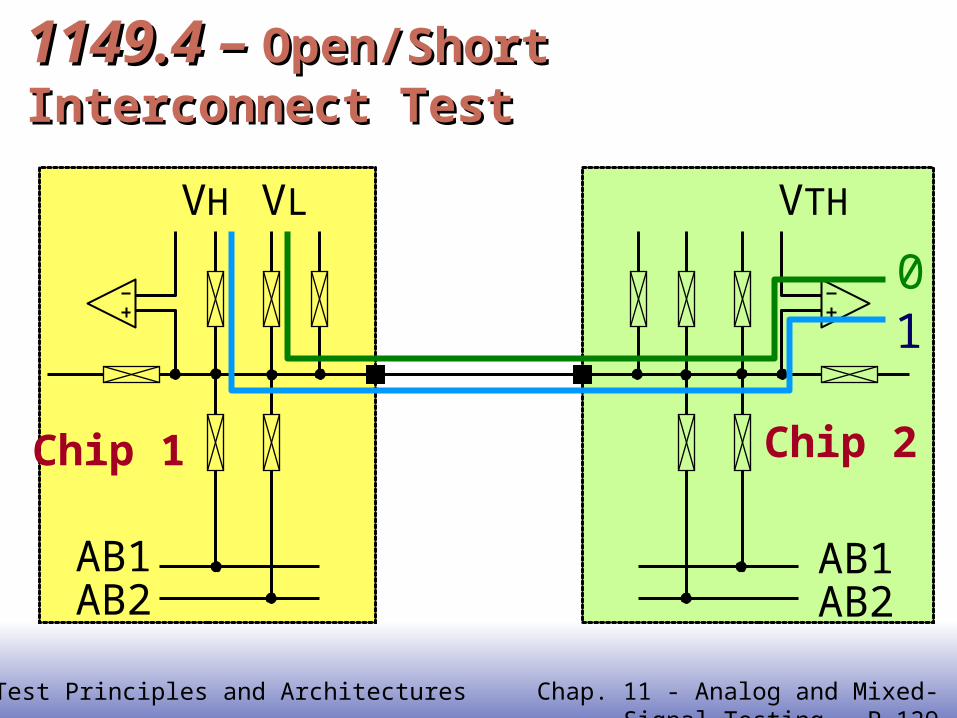
1149.4 – 1149.4 – Open/Short Interconnect TestOpen/Short Interconnect Test
AB1AB2
VH VL
AB1AB2
VTH
Chip 1 Chip 2
10
EE141VLSI Test Principles and Architectures Chap. 11 - Analog and Mixed-Signal Testing - P.130
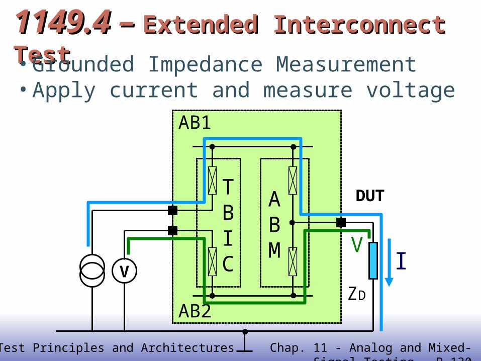
1149.4 – 1149.4 – Extended Interconnect TestExtended Interconnect Test
AB1
AB2
TBIC
ABM
V
DUT
IV
• Grounded Impedance Measurement• Apply current and measure voltage
ZD

EE141VLSI Test Principles and Architectures Chap. 11 - Analog and Mixed-Signal Testing - P.131
1149.4 – 1149.4 – Extended Interconnect TestExtended Interconnect Test
• Equivalent Circuit Model.
M
SIOR
SVIR
)(tIs
)(tVm
1PZ
2PZ
DUTZ DUTI
DUTV
DUTPSIO
SIOsDUT ZZR
RtItI
1)()(
DUTPSVI
SVIDUTM ZZR
RtVtV
2)()(

EE141VLSI Test Principles and Architectures Chap. 11 - Analog and Mixed-Signal Testing - P.132
1149.4 – 1149.4 – Extended Interconnect TestExtended Interconnect Test
AB1
AB2
TBIC
ABM
VDUT
VG
I
V
• Floating Impedance Zd Measurement
ZD

EE141VLSI Test Principles and Architectures Chap. 11 - Analog and Mixed-Signal Testing - P.133
1149.4 – 1149.4 – Extended Interconnect TestExtended Interconnect Test
AB1
AB2
TBIC
ABM
V
DUT
VG
I
V
Vg Option withNonzero Vg
• Floating Impedance ZD with optional Vg
ZD

EE141VLSI Test Principles and Architectures Chap. 11 - Analog and Mixed-Signal Testing - P.134
TBIC
ABM
VABM
TBIC
• Apply voltage and measure current
ZD
1149.4 – 1149.4 – Extended Interconnect TestExtended Interconnect Test

EE141VLSI Test Principles and Architectures Chap. 11 - Analog and Mixed-Signal Testing - P.135
• Equivalent Circuit Model
1149.4 – 1149.4 – Extended Interconnect TestExtended Interconnect Test
SIIR)(tIm
V
SVOR
)(tVs
1PZ
2PZ
DUTZ
DUTV
DUTI
M
SIIPDUTPSVO
DUTsDUT RZZZR
ZtVtV
21)()(
SIIPDUTPSVO
sm RZZZR
tVtI
21
)()(
21)()(
PDUTP
DUTsDUT ZZZ
ZtVtV
21
)()(
PDUTP
sm ZZZ
tVtI
With Ideal Voltage Source and Current Meter

EE141VLSI Test Principles and Architectures Chap. 11 - Analog and Mixed-Signal Testing - P.136
• Measure complex interconnect network
V
P1
P2 P4
P3
Z1Z2
Z3V34V12
V13
Vg
1149.4 – 1149.4 – Extended Interconnect TestExtended Interconnect Test
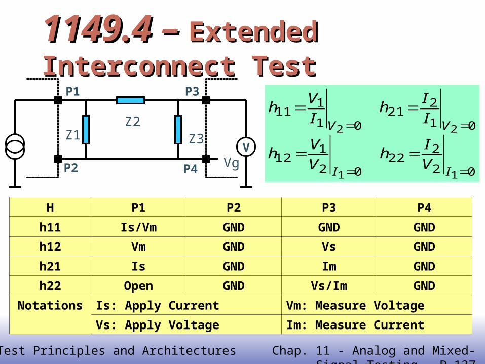
EE141VLSI Test Principles and Architectures Chap. 11 - Analog and Mixed-Signal Testing - P.137
V
P1
P2 P4
P3
Z1Z2
Z3
Vg
1149.4 – 1149.4 – Extended Interconnect TestExtended Interconnect Test
02
222
02
112
01
221
01
111
11
22
II
VV
V
Ih
V
Vh
I
Ih
I
Vh
H P1 P2 P3 P4
h11 Is/Vm GND GND GND
h12 Vm GND Vs GND
h21 Is GND Im GND
h22 Open GND Vs/Im GND
Notations Is: Apply Current Vm: Measure Voltage
Vs: Apply Voltage Im: Measure Current
EE141VLSI Test Principles and Architectures Chap. 11 - Analog and Mixed-Signal Testing - P.138
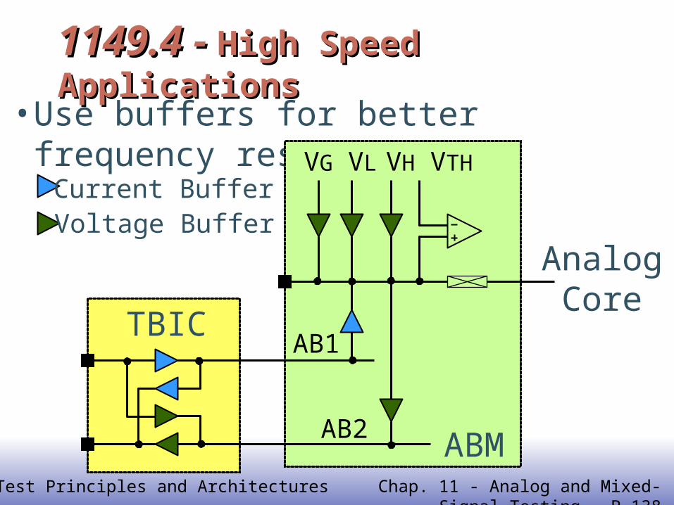
1149.4 - 1149.4 - High Speed ApplicationsHigh Speed Applications
• Use buffers for better frequency response
AB2
VHVL VTHVG
AB1TBIC
ABM
AnalogCore
Current BufferVoltage Buffer
EE141139
VLSI Test Principles and Architectures Chap. 11 - Analog and Mixed-Signal Testing - P.139
11.5 Concluding Remarks11.5 Concluding Remarks AMS testing requires specialized approaches
and experienced engineers because of the large varieties of signals, functions and circuits.
DSP approaches are so pervasive that even basic analog test items can be accomplished.
IEEE 1057 with formal terminologies and standardized test methods provides a solid theoretical background for ADC/DAC testing.
IEEE 1149.4 is one solution to extending and incorporating the digital counterpart.