Embed Size (px)
DESCRIPTION
A very good informative read on Electronmigration related issues
Citation preview
3/10/2015 EE Times Addressing signal electromigration (EM) in today's complex digital designs
http://www.eetimes.com/document.asp?doc_id=1280370&print=yes 1/9
Geetha Rangarajan – Synopsys, JamesDeng – Altera1/28/2013 03:53 PM EST 1 Comment
Tweet 0 0
Design HowTo
Addressing signal electromigration (EM) intoday’s complex digital designs
AbstractElectromigration (EM) is a phenomenon that has been well researchedand understood by the design community. At mature nodes, its impacton digital integrated circuits, particularly signal interconnects, has beenminimal, making signal EM analysis and fixing an optional design step.At 28 nm and beyond, this is no longer the case. Interconnects aregetting thinner, running longer and switching at gigahertz speeds all ofwhich amplify the effects of EM. Signal EM analysis and fixing is turninginto a design requirement that must be met during place and route. This article discusses the importance of signal EM and ways to addressit in today’s complex designs. It also highlights the EM capabilities in ICCompiler with results from Altera’s successful adoption of the solutionfor its 28nm high performance IPs.
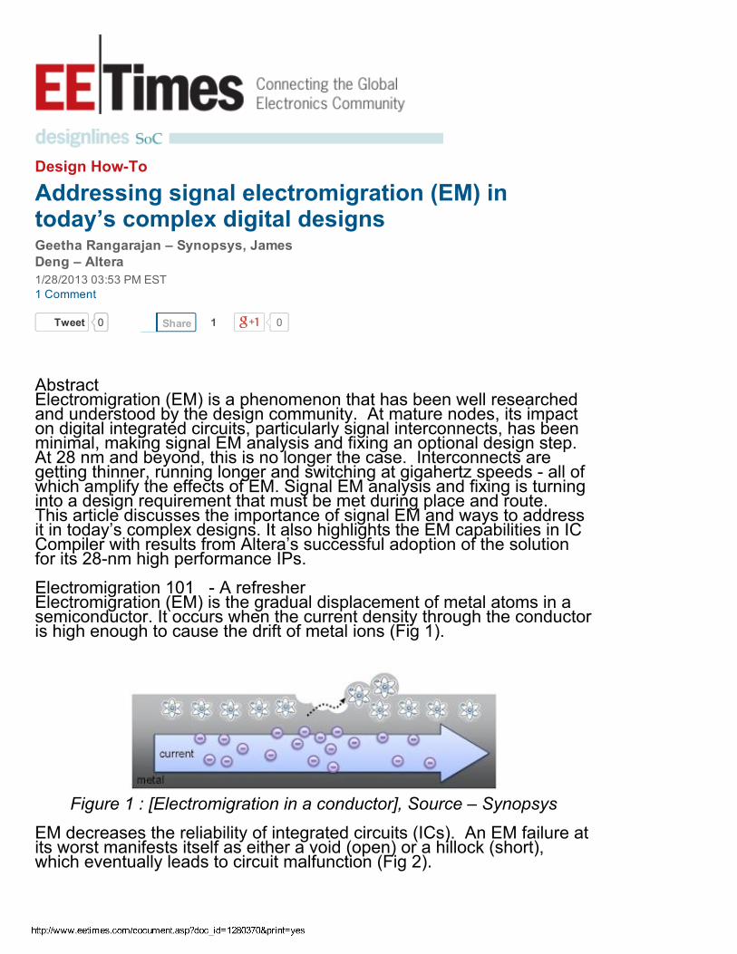
Electromigration 101 A refresherElectromigration (EM) is the gradual displacement of metal atoms in asemiconductor. It occurs when the current density through the conductoris high enough to cause the drift of metal ions (Fig 1).
Figure 1 : [Electromigration in a conductor], Source – Synopsys
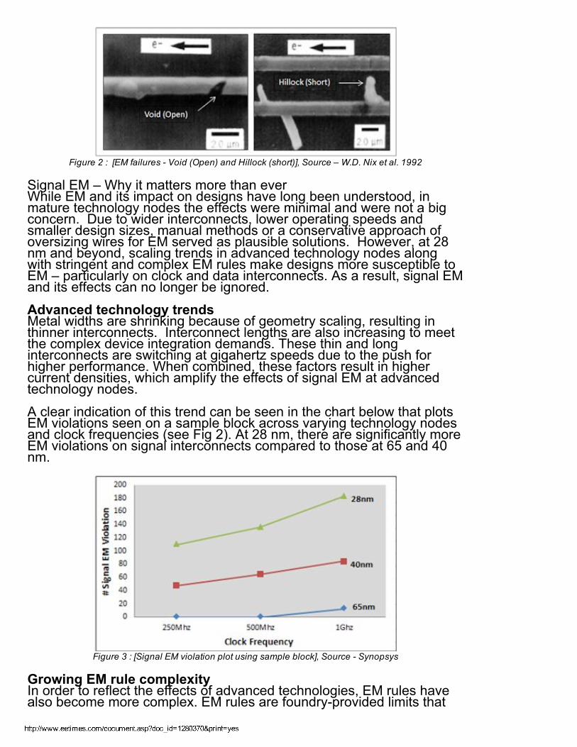
EM decreases the reliability of integrated circuits (ICs). An EM failure atits worst manifests itself as either a void (open) or a hillock (short),which eventually leads to circuit malfunction (Fig 2).
Share 1
3/10/2015 EE Times Addressing signal electromigration (EM) in today's complex digital designs
http://www.eetimes.com/document.asp?doc_id=1280370&print=yes 2/9
Figure 2 : [EM failures Void (Open) and Hillock (short)], Source – W.D. Nix et al. 1992
Signal EM – Why it matters more than ever While EM and its impact on designs have long been understood, inmature technology nodes the effects were minimal and were not a bigconcern. Due to wider interconnects, lower operating speeds andsmaller design sizes, manual methods or a conservative approach ofoversizing wires for EM served as plausible solutions. However, at 28nm and beyond, scaling trends in advanced technology nodes alongwith stringent and complex EM rules make designs more susceptible toEM – particularly on clock and data interconnects. As a result, signal EMand its effects can no longer be ignored.
Advanced technology trends Metal widths are shrinking because of geometry scaling, resulting inthinner interconnects. Interconnect lengths are also increasing to meetthe complex device integration demands. These thin and longinterconnects are switching at gigahertz speeds due to the push forhigher performance. When combined, these factors result in highercurrent densities, which amplify the effects of signal EM at advancedtechnology nodes.
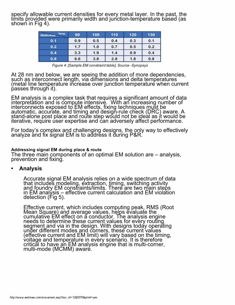
A clear indication of this trend can be seen in the chart below that plotsEM violations seen on a sample block across varying technology nodesand clock frequencies (see Fig 2). At 28 nm, there are significantly moreEM violations on signal interconnects compared to those at 65 and 40nm.
Figure 3 : [Signal EM violation plot using sample block], Source Synopsys
Growing EM rule complexity In order to reflect the effects of advanced technologies, EM rules havealso become more complex. EM rules are foundryprovided limits that
3/10/2015 EE Times Addressing signal electromigration (EM) in today's complex digital designs
http://www.eetimes.com/document.asp?doc_id=1280370&print=yes 3/9
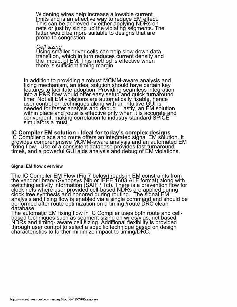
specify allowable current densities for every metal layer. In the past, thelimits provided were primarily width and junctiontemperature based (asshown in Fig 4).
Figure 4: [Sample EM constraint table], Source Synopsys
At 28 nm and below, we are seeing the addition of more dependencies,such as interconnect length, via dimensions and delta temperatures(metal line temperature increase over junction temperature when currentpasses through it).
EM analysis is a complex task that requires a significant amount of datainterpretation and is compute intensive. With an increasing number ofinterconnects exposed to EM effects, fixing techniques must beautomatic, accurate, and timing and designrule check (DRC) aware. Astandalone post place and route step would not be ideal as it would beiterative, require user expertise and can adversely affect performance.
For today’s complex and challenging designs, the only way to effectivelyanalyze and fix signal EM is to address it during P&R.
Addressing signal EM during place & routeThe three main components of an optimal EM solution are – analysis,prevention and fixing.
• Analysis
Accurate signal EM analysis relies on a wide spectrum of datathat includes modeling, extraction, timing, switching activityand foundry EM constraints/limits. There are two main stepsin EM analysis – effective current calculation and EM violationdetection (Fig 5).
Effective current, which includes computing peak, RMS (RootMean Square) and average values, helps evaluate thecumulative EM effect on a conductor. The analysis engineneeds to determine these current values for every routingsegment and via in the design. With designs today operatingunder different modes and corners, these current values(effective current and EM limit) will vary based on the timing,voltage and temperature in every scenario. It is thereforecritical to have an EM analysis engine that is multicorner,multimode (MCMM) aware.

3/10/2015 EE Times Addressing signal electromigration (EM) in today's complex digital designs
http://www.eetimes.com/document.asp?doc_id=1280370&print=yes 4/9
Figure 5: [Components of Signal EM Analysis], Source: Synopsys
Once effective current values are determined, an EM violationis detected based on the current limits derived from thefoundry EM constraints (Fig 6).
Figure 6: [EM Violation Detection], Source: Synopsys
PreventionPrevention can be implemented for signals that have anincreased probability for EM violation. For instance, due totheir high toggle rates and large drive cells, clock nets aremore at risk for EM than data nets. Clock nets with specialwidth and spacing rules (NDRs) derived from their driver cellscan help minimize the impact of EM. When applied duringclock tree synthesis and honored during route, these NDRsenable a correct by construction approach to minimizeunnecessary perturbation on the clock nets during signalrouting
• Fixing
EM fixing is a function of sizing wires, vias and cells in orderto effectively reduce the current density through them. Acomprehensive fixing solution much like analysis would alsoneed to be MCMMaware. Two commonly used EM fixingapproaches are wire widening and cell sizing.
Wire widening
3/10/2015 EE Times Addressing signal electromigration (EM) in today's complex digital designs
http://www.eetimes.com/document.asp?doc_id=1280370&print=yes 5/9
Widening wires help increase allowable currentlimits and is an effective way to reduce EM effect.This can be achieved by either applying NDRs onnets or just by sizing up the violating segments. Thelatter would be more suitable to designs that areprone to congestion.
Cell sizingUsing smaller driver cells can help slow down datatransition, which in turn reduces current density andthe impact of EM. This method is effective whenthere is sufficient timing margin.
In addition to providing a robust MCMMaware analysis andfixing mechanism, an ideal solution should have certain keyfeatures to facilitate adoption. Providing seamless integrationinto a P&R flow would offer easy setup and quick turnaroundtime. Not all EM violations are automatically fixable, henceuser control on techniques along with an intuitive GUI isneeded for faster analysis and debug. Lastly, an EM solutionwithin place and route is effective only when it is accurate andconvergent, making correlation to industrystandard SPICEsimulators a must.
IC Compiler EM solution Ideal for today’s complex designs IC Compiler place and route offers an integrated signal EM solution. Itprovides comprehensive MCMMaware analysis and an automated EMfixing flow. Use of a consistent database provides fast turnaroundtimes, and a powerful GUI aids analysis and debug of EM violations.
Signal EM flow overview
The IC Compiler EM Flow (Fig 7 below) reads in EM constraints fromthe vendor library (Synopsys plib or IEEE 1603 ALF format) along withswitching activity information (SAIF / Tcl). There is a prevention flow forclock nets where user provided cellbased NDRs are applied duringclock tree synthesis and honored during routing. The signal EManalysis and fixing flow is enabled via a single command and should beperformed after route optimization on a timing /route DRC cleandatabase.The automatic EM fixing flow in IC Compiler uses both route and cellbased techniques such as segment sizing on wires/vias, net basedNDRs and timing aware cell sizing. Additional flexibility is providedthrough user control to select a specific technique based on designcharacteristics to further minimize impact to timing/DRC.

3/10/2015 EE Times Addressing signal electromigration (EM) in today's complex digital designs
http://www.eetimes.com/document.asp?doc_id=1280370&print=yes 6/9
Figure 7: [IC Compiler Signal EM Flow], Source: Synopsys
Most importantly, IC Compiler’s EM analysis is well correlated toHSPICE, offering an accurate and convergent solution for today’schallenging designs.
Altera’s experience using IC Compiler EM solutionGroup background Located in Altera’s headquarters in San Jose, Calif., the physical designengineering team managed by James Deng supports multiple RTL frontend teams for netlist to GDSII support and helps define implementationmethodology for their highperformance designs. The team waschartered with implementing all the RTLbased IP and subsystem inAltera’s first highperformance 28nm FPGA (Stratix V). In order toensure that the reliability of their device was not compromised, the teamdecided to perform signal EM analysis for the first time ever and choseto use IC Compiler.
Design details and challengesThe design targeted for signal EM analysis was a PCI IP, which had ahierarchical implementation with 11 sub blocks partitioned for IP reuse(Fig 8) operating at 500+ Mhz.

3/10/2015 EE Times Addressing signal electromigration (EM) in today's complex digital designs
http://www.eetimes.com/document.asp?doc_id=1280370&print=yes 7/9
Figure 8: [Altera's 28nm PCI IP Floorplan], Source: Altera
Since the programmable IP had many functional modes and complexclock structures, MCMMaware EM analysis was a must. The highaspect ratio of certain blocks also made them prone to routingcongestion, which meant a conservative approach to EM fixing was notviable.
Altera’s EM flow To prevent excessive EM violations post route, Altera chose to useNDRs on clock nets during CTS and followed with IC Compiler’s signalEM analysis and fixing flow after routing. Different MCMM scenarioswere created for EM analysis in order to achieve the mostcomprehensive coverage. The segmentbased fixing approach in ICCompiler was selected due to the high routing congestion in the design.
Results
IC Compiler’s automatic signal EM flow was able to fix the majority ofthe violations with minimal DRC impact. Shown below (Fig 9) are resultsfrom two of the PCI IP blocks.
Figure 9: [Altera's Signal EM Results using IC Compiler], Source: Altera
A few violations were left unfixed due to congestion and were lateraddressed manually by designers.
Altera also found IC Compiler’s GUI features very useful and intuitive to

3/10/2015 EE Times Addressing signal electromigration (EM) in today's complex digital designs
http://www.eetimes.com/document.asp?doc_id=1280370&print=yes 8/9
view the EM current density maps and understand the hot spots in thedesign (Fig 10).
Figure 10: [IC Compiler EM Current Density Map], Source: Altera
Furthermore, the report files provided clear and detailed information,making it simpler for the firsttime user to comprehend the data (Fig 11).
Figure 11: [IC Compiler EM Summary File], Source: Altera
Altera successfully ran IC Compiler’s signal EM flow on all the blocks intheir first 28nm FPGA chip and has now deployed it as part of theirproduction flow.
Altera’s Design Engineering Manager, James Deng had this to saybased on their experience “We found that IC Compiler’s signal EM flowprovided an easy solution with clear reporting and automatic fixingmethodology. The MCMM feature in Signal EM was very useful to us. Itreduced the risk of merging scenarios ad avoided pessimistic/optimisticanalysis. We recommend using IC Compiler to check and clean allsignal EM violations before signoff”.
ConclusionAt 28 nm and beyond, geometry scaling and higher frequencies havemade EM failures not just a possibility but a reality for every design. Signal EM analysis has become an integral part of physical designmethodology. As experienced by Altera, IC Compiler provides an easytouse, accurate and comprehensive EM solution that addresses theneeds of today’s complex and challenging designs.
AcknowledgementsThe authors would like to acknowledge the invaluable efforts of theircolleagues, Kevin Huang at Altera and Rajiv Dave at Synopsys, whohave helped in providing the data for this article.
About the authors

3/10/2015 EE Times Addressing signal electromigration (EM) in today's complex digital designs
http://www.eetimes.com/document.asp?doc_id=1280370&print=yes 9/9
EMAIL THIS PRINT COMMENT
Geetha Rangarajan is a senior technical marketingmanager for IC Compiler at Synopsys. She has over 15years of experience in the ASIC and semiconductorindustry. Prior to Synopsys, she worked at LSI as anASIC design engineer focusing on place and route,design for test and static timing analysis for several keynetworking and storage designs. Before that, sheworked at Texas Instruments on the librarycharacterization team. Rangarajan holds a bachelor ofengineering degree in electronics and communicationengineering from Coimbatore, India.
James Deng is the physical design engineeringmanager at Altera. He is responsible for developingASICstyle physical design solutions, andimplementation of high performance digital IPs atcuttingedge technology node. He has over 16 years ofexperience in ASIC/SoC/FPGA semiconductorindustry. Before joining Altera, he worked at BayMicrosystem on network processor (NPU) design andverification. He also worked at LSI Logic as seniorASIC design engineer developing advanced ASICsfrom RTL to GDS. James holds MSEE degree in VLSI
circuit design and computer engineer area from Purdue University and aBE degree from Tsinghua University in China.
If you found this article to be of interest, visit EDA Designline whereyou will find the latest and greatest design, technology, product, andnews articles with regard to all aspects of Electronic Design Automation(EDA).
Also, you can obtain a highlights update delivered directly to your inboxby signing up for the EDA Designline weekly newsletter – just ClickHere to request this newsletter using the Manage Newsletters tab (if youaren't already a member you'll be asked to register, but it's free andpainless so don't let that stop you).
More Related LinksIntel's 1st Xeon SoC Twists ARM
Shifting Mindsets: Static Verification Transforms SoC Design at RT Level
Graphics API Gets Makeover
Intel Tablet SoCs Pack LTE
Asian Share of Global Fab Capacity May Top 69% by 2019
Copyright © 2015 UBM Electronics, A UBM company, All rights reserved. Privacy Policy | Terms of Service


