Embed Size (px)
Citation preview

ECE Senior Project
CMOS Camera System-on-a-Chip

TEAM MEMBERS
Anil Kumar Angana Sheth Saurabh Desai George Moran Jason Moffa Takashi Ishihara ADVISOR: Dr. Brita Olson
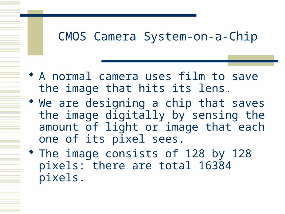
CMOS Camera System-on-a-Chip
A normal camera uses film to save the image that hits its lens.
We are designing a chip that saves the image digitally by sensing the amount of light or image that each one of its pixel sees.
The image consists of 128 by 128 pixels: there are total 16384 pixels.

PROJECT DIAGRAM
128 x128

Design Goals
• 128 x 128 CMOS APS (Act ive P ixel S ensor ) Phot o Diode P ixel s at a 12um pit ch
• .5 mm AMI 3 .3V / 5V Pr ocess • 20 MHz Mast er Cl ock • >60 f r ames/sec (1 .2 Mpix/sec maximum pixel
out put r at e ) • On-chip Cor r el at ed doubl e sampl ing • Ant i-bl ooming cir cuit r y • Diff er ent ial Anal og out put • Minimize power consumpt ion

Establishing a Chip Design Infrastructure
• Learning VLSI Design
• Learning VLSI Design Tools and Chip Design Process
• Establishing a Chip Design Flow at CPP
Configuring tools

Progress
Calculations/Analysis:
Floor Planning Conversion Gain
Parasitics /Loading Noise
Component Development:
Design Optimization, Simulation with loading, Port to new environment
Decoder primitive Anti-blooming CircuitryDecoder Bus Driver Row driver: Row RST & SEL DriverAnti-blooming Circuitry Amplifier Bias Circuitry
Pixel Analog Signal Chain Sample & Hold Circuit

Progress (cont.)
Chip Level Design:Pixel Array schematic
In progress:7-bit decoder
Analog Signal Chain with Correlated Double Sampling

Accomplished Tasks
Floor Planning
7 Bit Decoder
Anti Blooming Circuitry

16 pads
FLOOR PLANNING
128*128Imager
Pitch = 150um
3mm
3m
m
136*12um
16
pad
s
The floor plan estimates the area of major units in the chip and defines their relative placements.
The floor plan is essential to determine whether a proposed design will fit in the chip area budgeted and to estimate wiring lengths and wiring congestion, so an initial floor plan should be prepared as soon as the logic is loosely defined.
Pitch: It is a distance between two pads.
Pads: They are wired to the pins on the chip package. They are for the I/O connection on the chip
4 AMI 0.5um Tiny ChipsPackaging : 150um pad pitchPixels : 12um pitch

ROW
DRIVERS
ROW
DECODER
READOUT CIRCUITS
COLUMN DECODER
APS Architecture
128*128 PIXEL ARRAY
A decoder is a Combinational circuit, when enabled, produces one of 2n minterms or maxterms at the output based on the input Combinations.
Row Decoder: Selects row for readout.
Column Decoder: Controls readout of Pixels In given row.
Row[i]12827=128
128
27=128

Row-add<0:6> Row-add<0:6>
Selects row 0
Selects row 1
0000000
1000000
Decoder Implementation
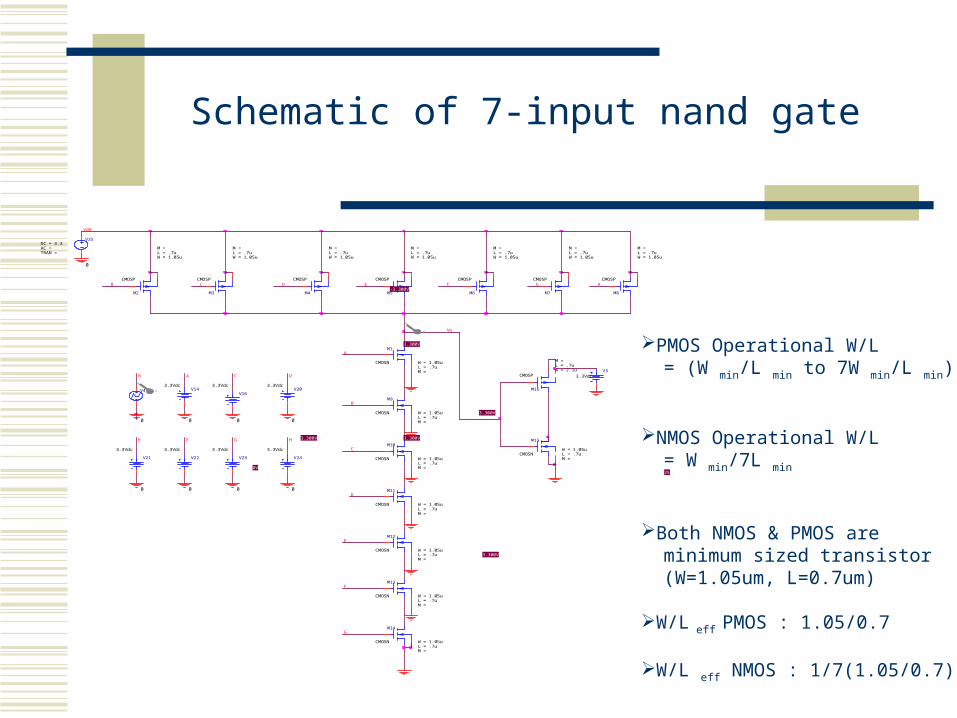
A 7 input nand gate based implementation results in a compact and regular realization reducing development time and cost.
The chip that we are designing has 128*128 pixels so the decoder consists of 128 of 7 input nand gates.

Decoder Design Requirements
Master Clock = 20MHz
Trise/Fall requirements are relaxed.
In our design Trise/Fall times are 50% of clock. Trise/Fall = ½(1/20MHz) = 25ns
V25
AC =TRAN =
DC = 3.3
M1
CMOSN W = 1.05uL = .7uM =
0
M2
CMOSP
W = 1.05uL = .7uM =
M3
CMOSP
W = 1.05uL = .7uM =
vdd
M4
CMOSP
W = 1.05uL = .7uM =
M5
CMOSP
W = 1.05uL = .7uM =
M6
CMOSP
W = 1.05uL = .7uM =
M7
CMOSP
W = 1.05uL = .7uM =
M8
CMOSP
W = 1.05uL = .7uM =
0
0
M9
CMOSN W = 1.05uL = .7uM =
M10
CMOSN W = 1.05uL = .7uM =
M11
CMOSN W = 1.05uL = .7uM =
M12
CMOSN W = 1.05uL = .7uM =
M13
CMOSN W = 1.05uL = .7uM =
M14
CMOSN W = 1.05uL = .7uM =
B
0V
Vo
V33.3VdcB
A
3.300V
A
3.300V
-3.300V
C D
3.300V
B
E F G
C
V
V
GC
D
3.300V
M15
CMOSNW = 1.05uL = .7uM =
M16
CMOSPW = 2.1uL = .7uM =
D
3.300V
E F
25.49nV
A
3.300V
0
H
V24
3.3Vdc
G
F
E
V4
0
V143.3Vdc
V16
3.3VdcV20
3.3Vdc
V21
3.3Vdc
V22
3.3Vdc
V23
3.3Vdc
0 0 0
0
Schematic of 7-input nand gate
PMOS Operational W/L = (W min/L min to 7W min/L min)
NMOS Operational W/L = W min/7L min
Both NMOS & PMOS are minimum sized transistor (W=1.05um, L=0.7um)
W/L eff PMOS : 1.05/0.7
W/L eff NMOS : 1/7(1.05/0.7)

Simulation for fall time when W = 1.05um
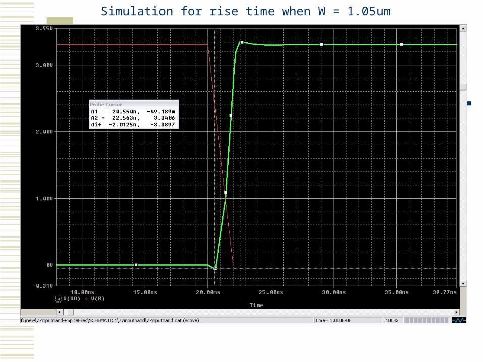
Simulation for rise time when W = 1.05um
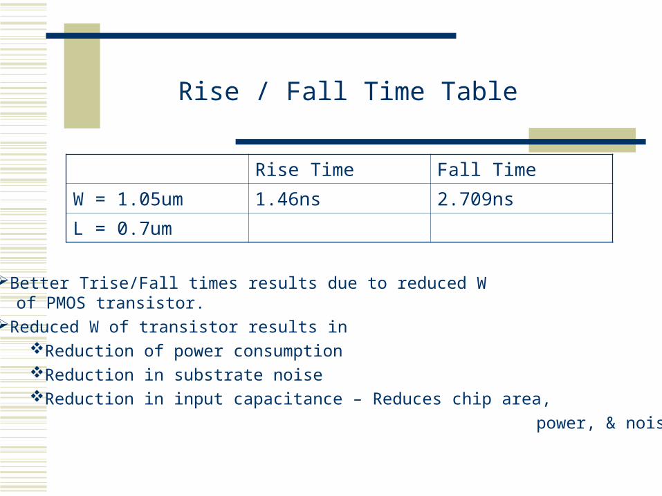
Rise / Fall Time Table
Rise Time Fall Time
W = 1.05um 1.46ns 2.709ns
L = 0.7um
Better Trise/Fall times results due to reduced W of PMOS transistor.Reduced W of transistor results in
Reduction of power consumptionReduction in substrate noiseReduction in input capacitance – Reduces chip area, power, & noise.
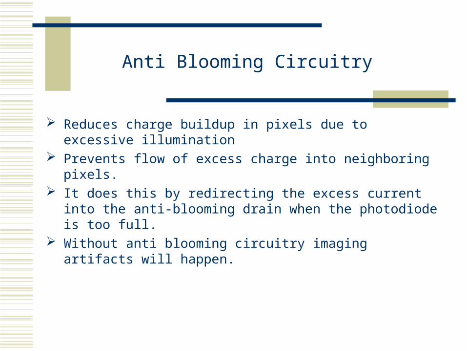
Anti Blooming Circuitry
Reduces charge buildup in pixels due to excessive illumination
Prevents flow of excess charge into neighboring pixels. It does this by redirecting the excess current into the
anti-blooming drain when the photodiode is too full. Without anti blooming circuitry imaging artifacts will
happen.

Anti Blooming CircuitryRow Driver
8 4
26
RST
Pixel
Floating Diffusion
FD
RST = 5VRST_LO = 1VVTH = 0.7V
Normal Imaging Condition: When RST signal is applied FD is around 2.8V and after integration of light it becomes 1.8V. (Vgs < VTH) = 1 – 1.8 < 0.7 - Transistor Off
Bright Light: Due to bright light FD decreases to 0.3V (Vgs >= VTH) = 1 – 0.3 >= 0.7 – Transistor on and excess carriers removed.
Anti Blooming Circuit Operation
Vdd
RST 5v
RST_LO = 1V
Integration

V70.8Vdc
0
0
0V
0V
+ IC= 3.3V
V
V
V33.3Vdc
M15
CMOSNW = 1.05uL = .7uM =
M16
CMOSP
W = 1.05u
L = .7uM =
0V
3.300VM17
CMOSNW = 1.05uL = .7uM =
M18
CMOSN
W = 1.05uL = .7uM = 128
B
A
V53.3Vdc
0
0
0
0
V6
0V
Anti Blooming Circuitry
Final stage of row driver Anti blooming circuitry

7 BIT INPUT SIGNAL DECODER DRIVER

Schematics
Driver (4x8x) Driving a load of 64, CMOS N and P transistors.
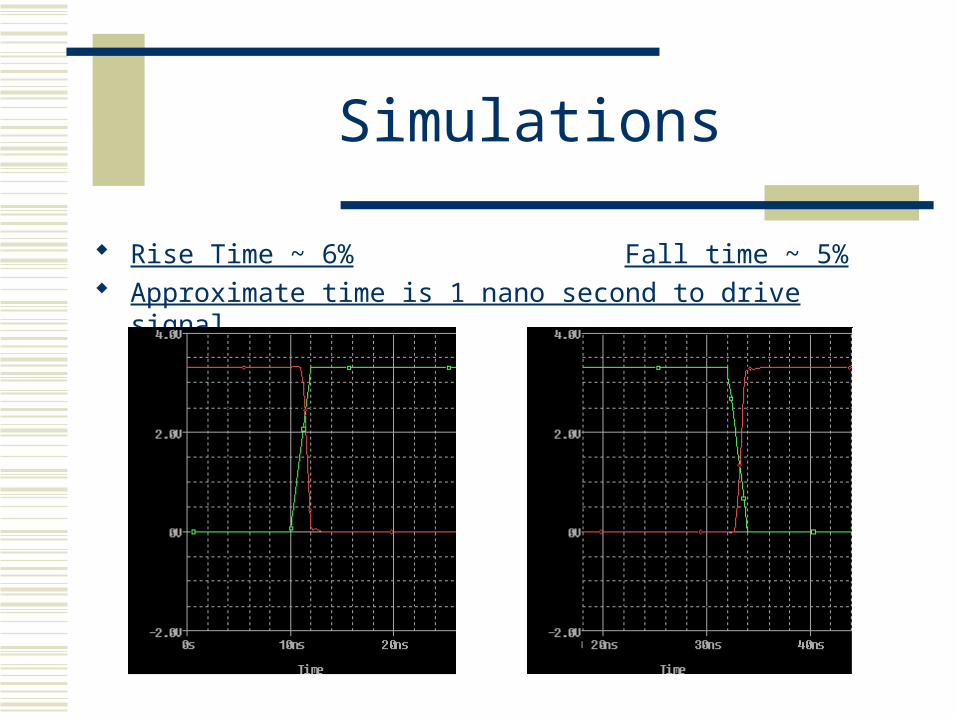
Simulations
Rise Time ~ 6% Fall time ~ 5% Approximate time is 1 nano second to drive signal.
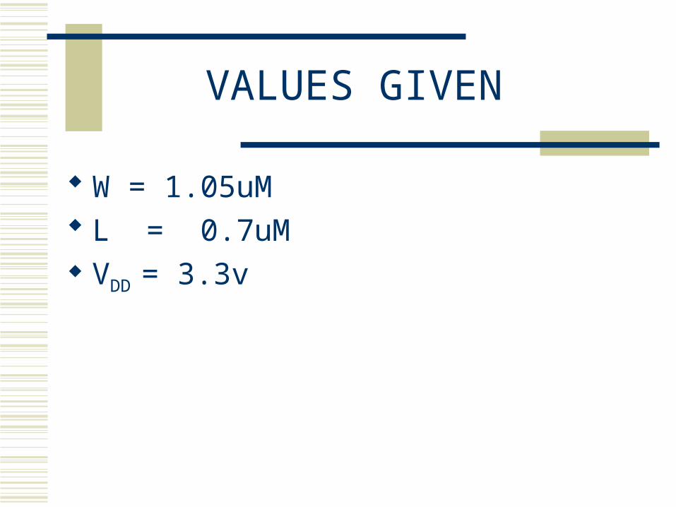
VALUES GIVEN
W = 1.05uM L = 0.7uM VDD = 3.3v
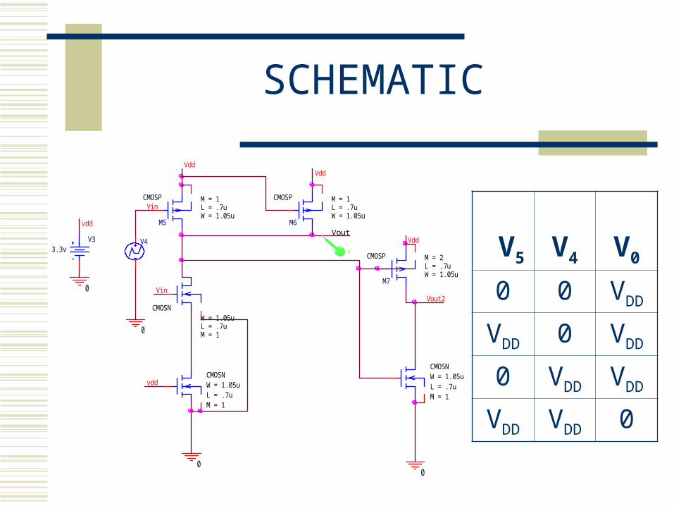
SCHEMATIC
CMOSNW = 1.05uL = .7uM = 1
CMOSNW = 1.05uL = .7uM = 1
0
Vout
Vin
0
Vin
vdd
V4
Vout2
M7
CMOSP
W = 1.05uL = .7uM = 2
CMOSNW = 1.05uL = .7uM = 1
0
Vdd
Vdd
0
V
V33.3v
vdd M5
CMOSP
W = 1.05uL = .7uM = 1
M6
CMOSP
W = 1.05uL = .7uM = 1
Vdd
V5
V4
V0
0 0 VDD
VDD 0 VDD
0 VDD VDD
VDD VDD 0

SCHEMATIC RESULT
Time
0s 0.2us 0.4us 0.6us 0.8us 1.0usV(M6:d)
-2.0V
0V
2.0V
4.0V
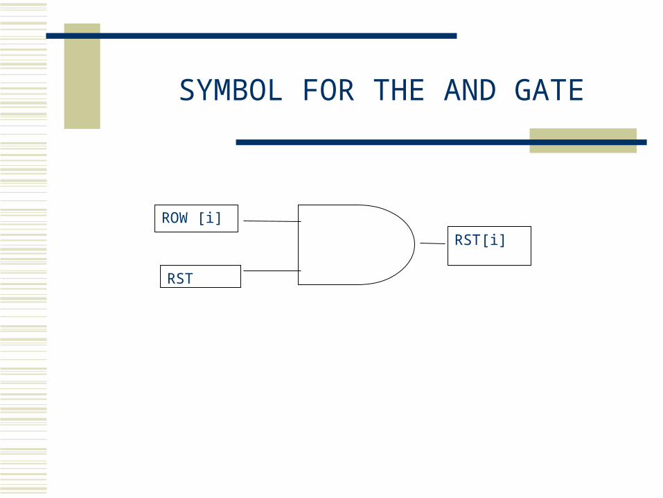
SYMBOL FOR THE AND GATE
ROW [i]
RST
RST[i]

Accomplished Tasks
1. Determine Resistive and Capacitive Parasitic Loading (Caused by dimension of the pixel Array)
2. Row Driver Design-Determine best combination for Drivers-Rise and Fall Times
-Reset Driver -Select Driver3. Simulations using PSPICE4. Implementation of Design using Cadence (LINUX)

Chip Schematic

Overview of Row Driver
SEL[i]SEL
ROW[i]
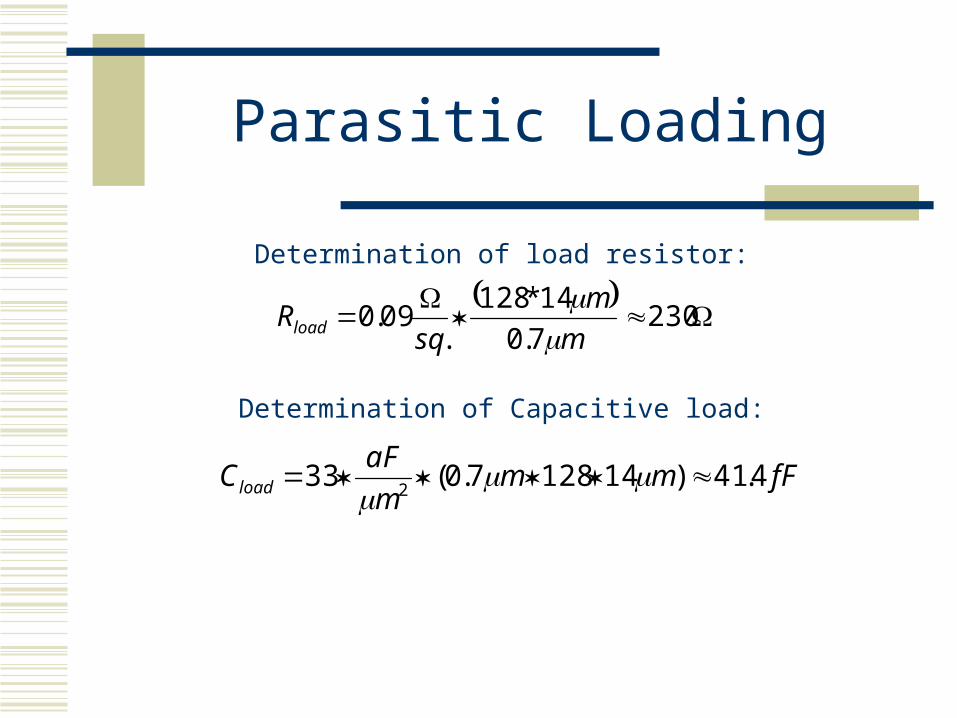
Parasitic Loading
Determination of load resistor:
Determination of Capacitive load:
fFmmm
aFCload 4.41)141287.0(33
2
230
7.0
14*128
.09.0
m
m
sqRload

The Row Driver
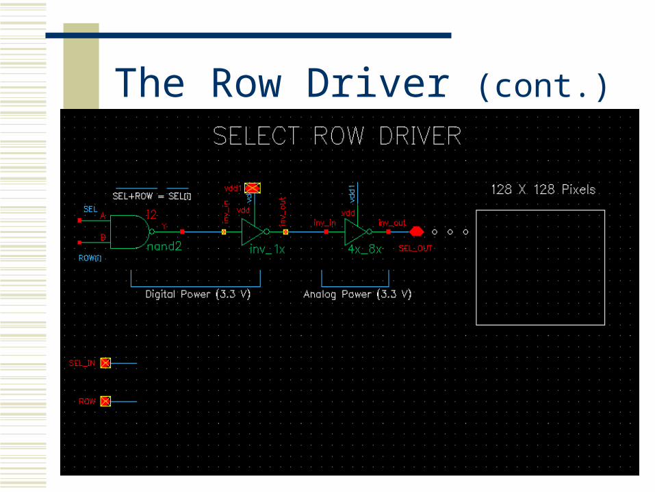
The Row Driver (cont.)

Simulations Summarized
Table 1: Rise and Fall Times for Inverter driving 128 transistors(using 102,400,402,600ns; Vdd=3.3V; Cload= 41.4fF)
Table 2: Rise and Fall times for inverters driving inv_8x
(using 102,400,402,600ns; Vdd=3.3V; Cload= 41.4fF)
Trial 1 Rise Time- 2outV(difference) Fall Time- 2outV(difference)
Inv_1xInv_8x -1.773n -1.676n Inv_2xInv_8x -1.100n -1.460n Inv_4xInv_8x -1.115n -1.380n
Trial 1 Rise Time-outV(difference) Fall Time-outV(difference) Inv_4x -2.10n -2.22n Inv_8x -1.42n -1.76n Inv_16x -971p -1.05n Inv_32x -768p -760p

Schematics
Two Drivers (4x_8x) Driving 128 CMOSN transistors
Vin1
V3Vout1
Simulated 128 Transistors
Inverter_4x Inverter_8x
Load Resistor
Load Capacitor
M1
CMOSN
W = 1.05uL = .7uM = 8
M2
CMOSPW = 2.10uL = .7uM = 8
vdd
gnd
V23.3Vdc
0
VV
CL41.4f
Vout2
Rl
230
M3
CMOSNW = 1.05uL = .7uM = 128
gndgndV4
1Vdc
M4
CMOSN
W = 1.05uL = .7uM = 4
M5
CMOSPW = 2.10uL = .7uM = 4
vdd
gnd

Simulations
Rise/Fall Times
Time
92.0ns 96.0ns 100.0ns 104.0ns 108.0ns 112.0ns 116.0ns89.1nsV(VIN1) V(VOUT2)
0V
1.0V
2.0V
3.0V
Time
380.0ns 390.0ns 400.0ns 410.0ns 420.0ns375.0ns 428.4nsV(VIN1) V(VOUT2)
0V
1.0V
2.0V
3.0V

Row Select Driver Design
Three Drivers (1x_4x_8x) Driving 128 CMOSN transistors
Vin1V5
V63.3Vdc
M6
CMOSN
W = 1.05uL = .7uM = 1
M7
CMOSPW = 2.10uL = .7uM = 1
gnd
vddvdd
Vout2Vout1
Simulated 128 Transistors
Inverter_8xLoad Resistor
Inverter_4x
Load Capacitor
Inverter_1x
V
V
M1
CMOSN
W = 1.05uL = .7uM = 8
M2
CMOSPW = 2.10uL = .7uM = 8
gnd
vdd
0
CL41.4f
Vout3R1
230
M3
CMOSNW = 1.05uL = .7uM = 128
gndgndV4
1Vdc
M4
CMOSN
W = 1.05uL = .7uM = 4
M5
CMOSPW = 2.10uL = .7uM = 4
vdd
gnd
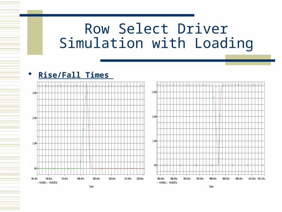
Row Select Driver Simulation with Loading
Rise/Fall Times
Time
90.0ns 95.0ns 100.0ns 105.0ns 110.0ns 115.0ns 120.0ns86.4nsV(VIN1) V(VOUT3)
0V
1.0V
2.0V
3.0V
Time
384.0ns 388.0ns 392.0ns 396.0ns 400.0ns 404.0ns 408.0ns 412.0ns 415.9nsV(VIN1) V(VOUT3)
0V
1.0V
2.0V
3.0V

Row Reset Driver Design
Introduction of two different power supply levels
Simulated 128 Transistors
Load Resistor
Inverter_4x
Inverter_8x
Load Capacitor
Inverter_1x NEW Power Source of 5V
Power Supply of 3.3 V
Vin1V5
V63.3Vdc
M6
CMOSN
W = 1.05uL = .7uM = 1
M7
CMOSPW = 2.10uL = .7uM = 1
vdd1vdd
gnd
Vout1
M1
CMOSN
W = 1.05uL = .7uM = 8
M2
CMOSPW = 2.10uL = .7uM = 8
vdd2
gnd
0
Vout3
CL41.4f
R1
230
M3
CMOSNW = 1.05uL = .7uM = 128
Vdd1
gndgndV4
1.8Vdc
M4
CMOSN
W = 1.05uL = .7uM = 4
M5
CMOSPW = 2.10uL = .7uM = 4
vdd2
gnd
V75Vdc
gnd
Vdd2
Vout2

Simulations
Rise/Fall Times
Time
90.00ns 95.00ns 100.00ns 105.00ns 110.00ns87.50ns 113.64nsV(VIN1) V(VOUT3)
0V
2.00V
4.00V
5.12V
Time
385ns 390ns 395ns 400ns 405ns 410ns 415ns 420ns 425nsV(VIN1) V(VOUT3)
0V
2.00V
4.00V
5.16V

General Chip Layout
IMAGER CHIP LAYOUT

Pixel & Timing Diagrams
ROW READOUT TIMINGS
PHOTODIODE PIXEL

Current Mirror Circuit To Bias Pixel SF
•“Large” gate widths and lengths used
•Good threshold matching
• gm reduced
L
m
C
gBWNoise
L
WI
VVC
L
WI
D
TNgsoxn
D
2
2
Current Equation
M1
CMOSN
W = 3uL = .7uM =
M2
CMOSN W = 3uL = 5.3uM =
M3
CMOSN W = 3uL = 5.3uM =
M4
CMOSNW = 5.8uL = 3uM =
M5
CMOSPW = 3uL = 5.3uM =
M6
CMOSP W = 3uL = 5.3uM =
M7
CMOSNW = 5.8uL = 3uM =
gate12
gate56
0
V13.3Vdc
vsource
0
R15k
V21Vdc
0
CL3p
gate34

M1
CMOSN
W = .9uL = .6uM =
M2
CMOSN
W = 1.2uL = .6uM =
M3CMOSN
W = 1.2uL = .6u
M =
M4CMOSNW = 3uL = 2uM =
M5
CMOSNW = 3u
L = 2uM =
V23.3Vdc
Vdd
SFout1
0
0
Vdd
Vdd
RST
0
0
00
C150f
VFD
C23p
0
0 C33p
Vout
I16uAdc
Vdd
0
VLN
V3 V
Determining Initial Condition For Sample & Hold Capacitor
•Optimize RST signal due to Body Effect
Pixel
Bias
Sample & Hold Capacitor
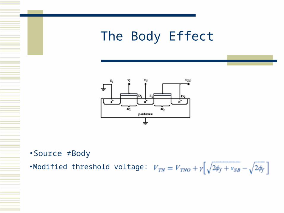
The Body Effect
•Source ≠Body
•Modified threshold voltage:
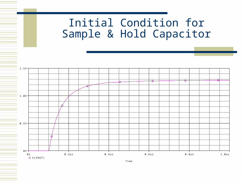
Time
0s 0.2us 0.4us 0.6us 0.8us 1.0usV(VOUT)
0V
0.5V
1.0V
1.5V
Initial Condition for Sample & Hold Capacitor

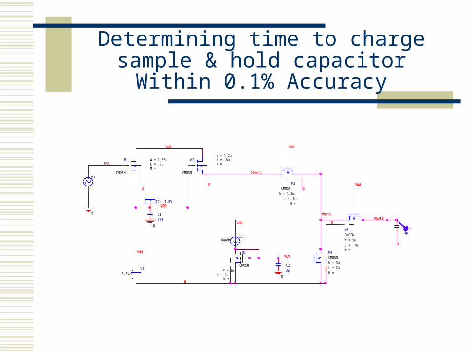
Determining Time to Discharge Sample & Hold Capacitor Within
0.1% Accuracy
M1
CMOSN
W = 1.05uL = .7uM =
M2
CMOSN
W = 1.2uL = .6uM =
M3CMOSN
W = 1.2uL = .6u
M =
M4CMOSNW = 3uL = 2uM =
M5
CMOSNW = 3u
L = 2uM =
V23.3Vdc
Vdd
SFout1
0
0
Vdd
Vdd
0
RST
0
00
C150f
VFD
C23p
0
0
C33p
Vout1
I16uAdc
Vdd
VLN
+ IC= 1.8V
M6CMOSNW = 5uL = .7uM =
Vout2
0
0
V3
sample
0
+ IC= 1.3V
V
•VFD initial condition: V = 1.8V
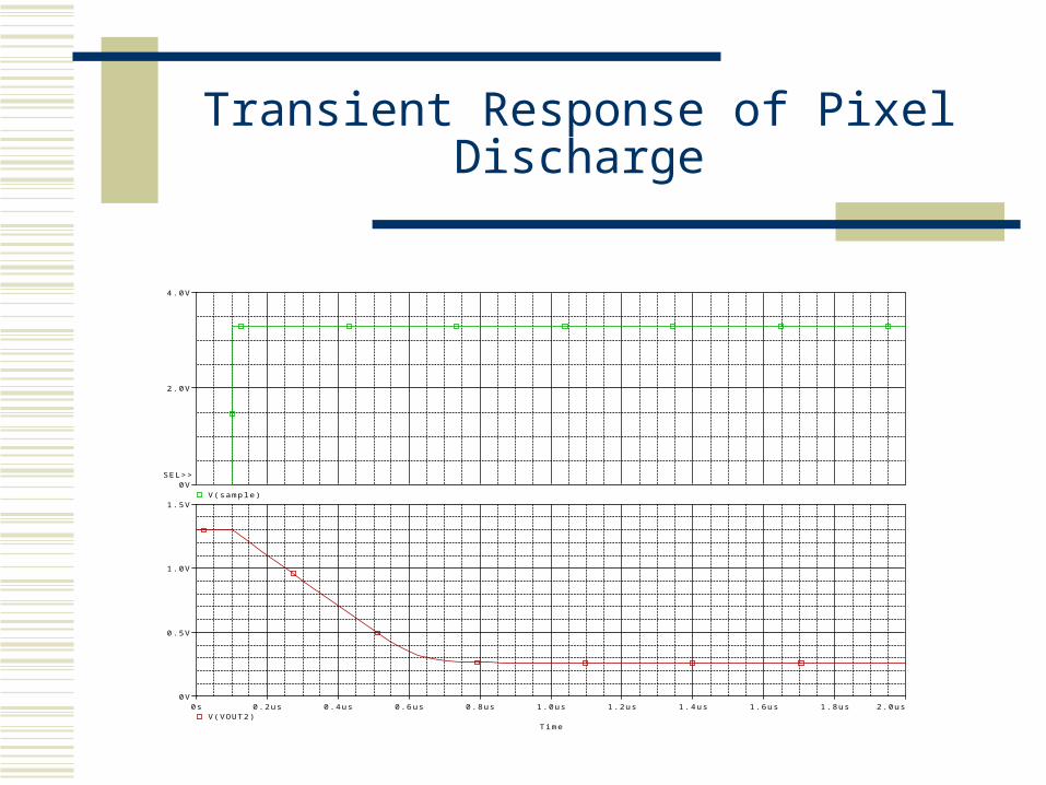
Transient Response of Pixel Discharge
Time
0s 0.2us 0.4us 0.6us 0.8us 1.0us 1.2us 1.4us 1.6us 1.8us 2.0usV(VOUT2)
0V
0.5V
1.0V
1.5VV(sample)
0V
2.0V
4.0V
SEL>>
Determining time to charge sample & hold capacitor Within
0.1% Accuracy
M1
CMOSN
W = 1.05uL = .7uM =
M2
CMOSN
W = 1.2uL = .6uM =
M3CMOSN
W = 1.2uL = .6u
M =
M4CMOSNW = 3uL = 2uM =
M5
CMOSNW = 3u
L = 2uM =
V23.3Vdc
Vdd
VFDVFDVFD
SFout1
00
Vdd
0
RST
Vdd
0
0
0
C150f
C23p
0
0 C33p
I16uAdc
Vdd
VLN
+ IC= 1.8V
M6CMOSNW = 5uL = .7uM =
0
0
V3
Vdd
Vout1Vout1
VFD
Vout2Vout2
V
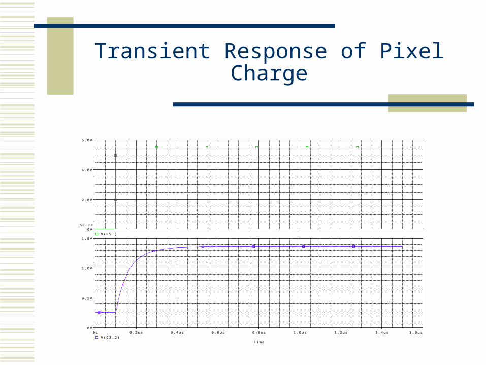
Transient Response of Pixel Charge
Time
0s 0.2us 0.4us 0.6us 0.8us 1.0us 1.2us 1.4us 1.6usV(C3:2)
0V
0.5V
1.0V
1.5VV(RST)
0V
2.0V
4.0V
6.0V
SEL>>

Accomplishments
• Designing output driver
• Determining the conversion gain
• Designing the pixel array

Output Driver
Pixel Array
Analog Sig. Chain ADC
Parasitic Capacitance
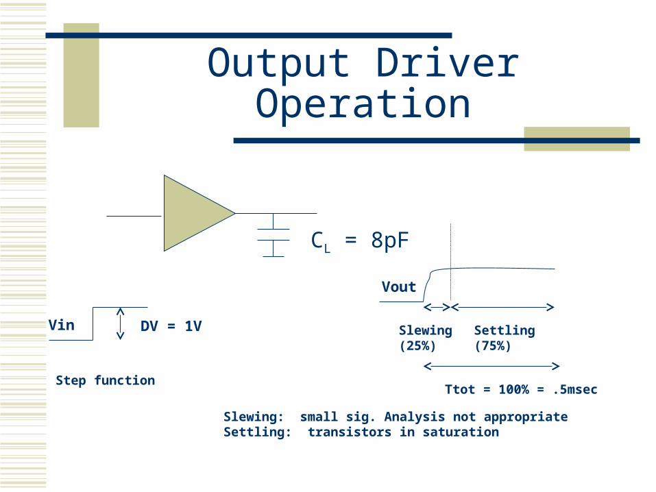
Output Driver Operation
Vin DV = 1V
Step function
Vout
Slewing(25%)
Settling(75%)
CL = 8pF
Ttot = 100% = .5msec
Slewing: small sig. Analysis not appropriateSettling: transistors in saturation
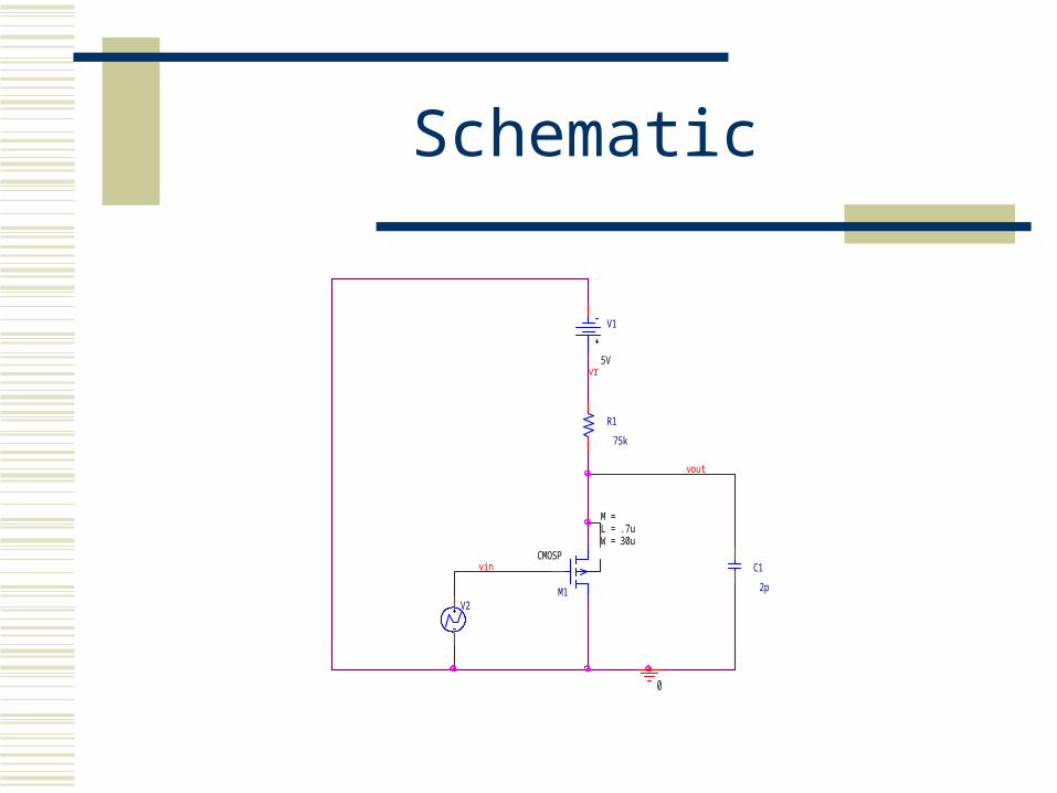
Schematic
vout
vr
V1
5V
vin C1
2p
V2
0
M1
CMOSPW = 30uL = .7uM =
R1
75k
Settling
R
Vin CL
Vout
0
LL CgmssCgmgmsAv
1
11||
1)(
Vin DV = 1V
Step function:
s
VsVin
)(
Amplifier transfer function:
Output:
/1)(1
1)()()( t
LO eVtVo
Cgmss
VsVinsAvsV
Settling accuracy
%1.7 settt
2/18'
'2
/7
VAkp
IkL
Wgm
gmC
Dp
L

Tfall output Driver (35uA)
Time
0s 100ns 200ns 300ns 400ns 500ns 600ns 700ns 800nsV(VOUT_2PF) V(VOUT_4PF) V(VOUT_8PF) V(VIN)
0V
1.0V
2.0V
3.0V
4.0V

Trise output Driver (35uA)
Time
0s 100ns 200ns 300ns 400ns 500ns 600ns 700ns 800nsV(VOUT_2PF) V(VOUT_4PF) V(VOUT_8PF) V(V2:+)
0.8V
1.2V
1.6V
2.0V
2.4V
2.8V
3.2V
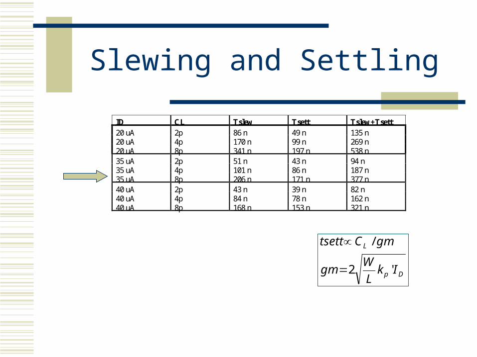
Slewing and Settling
ID CL Tslew Tsett Tslew+Tsett 20 uA 2p 86 n 49 n 135 n 20 uA 4p 170 n 99 n 269 n 20 uA 8p 341 n 197 n 538 n 35 uA 2p 51 n 43 n 94 n 35 uA 4p 101 n 86 n 187 n 35 uA 8p 206 n 171 n 377 n 40 uA 2p 43 n 39 n 82 n 40 uA 4p 84 n 78 n 162 n 40 uA 8p 168 n 153 n 321 n
Dp
L
IkL
Wgm
gmCtsett
'2
/

Conversion Gain
Cm
Cm(1-A)
C(total) = Cfd + Cm(1-A)
C.G.= Vout/Number of Electrons = q/C(total)
V = Q/C
Miller Effect
FACm
A
FCm
22
21
10*67.3)1(
8.0
10*84.1
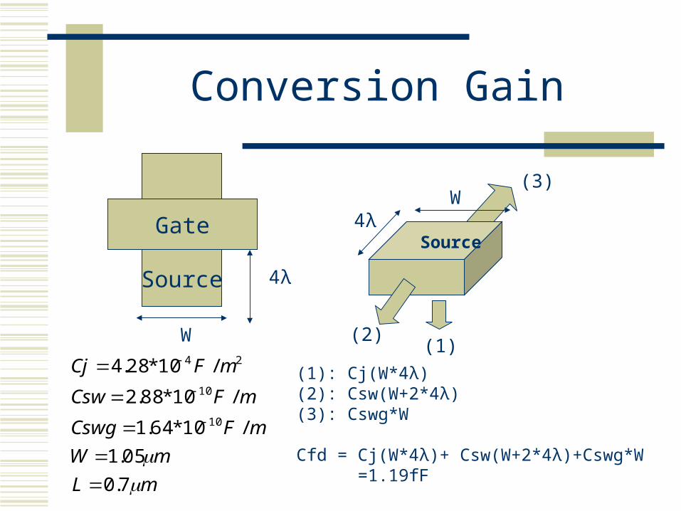
Conversion Gain
Gate
Source
W
4λ
W4λ
Source
(1)(2)
(3)
(1): Cj(W*4λ)(2): Csw(W+2*4λ)(3): Cswg*W
Cfd = Cj(W*4λ)+ Csw(W+2*4λ)+Cswg*W =1.19fFmL
mW
mFCswg
mFCsw
mFCj
7.0
05.1
/10*64.1
/10*88.2
/10*28.4
10
10
24

Conversion Gain
Vout
0.9 0.90.8
C(total)
C(total) = Cfd+Cm(1-A) = 1.19fF
Input: C.G.= q/C(total) = 134uV/electron
Output: C.G.= (0.8)(0.9)(0.9)(134u) = 87.1uV/electron

CHIP PROCESS

Remaining Tasks
Component development Optimization of Analog Signal chain with CDS
Chip Level Schematic DevelopmentCompletion of Decoder
Pad Ring
Assembly of final chip schematic
“Full” Chip Simulations
Layout

Acknowledgments
We wish t o acknowl edge S on V. Phan f or his inval uabl e ass is t ance and suppor t and Cal
Pol y Pomona f or pr oviding us wit h t he Cadence Des ign Tool s